H and T Intelligent Control HET-BC1024 Bluetooth Module User Manual
Shenzhen H&T; Intelligent Control Co., Ltd. Bluetooth Module Users Manual
Users Manual

Shenzhen H&T Intelligent Control Co., Ltd
Proprietary Information, No Dissemination or Use Allowed Without Prior Written Permission. All printed copies are considered Uncontrolled copies
unless the copies are stamped with “Controlled Copy” by Documentation Control.
HET-BC1024 User Manual
Summary
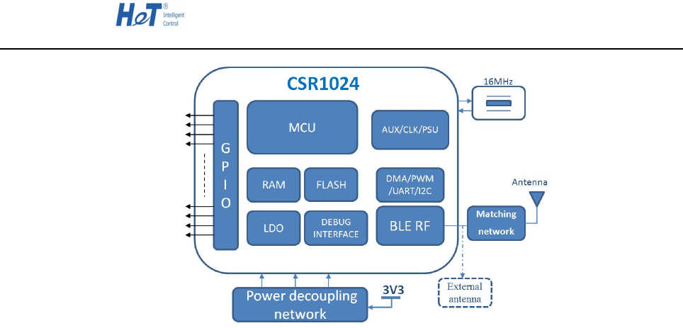
HET-BC1024 is a Bluetooth Low energy module, using CSR1024 as the main chip, which is a
built-in high efficiency and low-power processor. CSR1024 is able to run independently Bluetooth
5.0 protocol stack and application profile. HET-BC1024 has 80KB RAM and 192KB ROM with
256KB FLASH, also it has rich peripheral interfaces to meet different applications.
HET-BC1024 is an open development platform, users can design their own applications based
on the Bluetooth protocol stack, it also support a MESH network application and other typical
application-UART relay. Users can use the SDK of the module to shorten the development time
Applications
● Health Care
● Smart Home Application
● Motion Measurement
● Auto Electronics
● Leisure Toys
1. Brief Introduction
HET-BC1024 Bluetooth low energy module, using CSR1024 as the core processor. This module
is compatible with Bluetooth 5.0 specification,Runs in 2.4 GHz ISM band, GFSK modulation, 40
channel 2 MHz channel gap, three fixed radio channel, 37 automatic adaptive frequency hopping
data channel, 2 MHz gap better prevent adjacent channel interference. The internal PA can deliver a
maximum of 4dBm output, Receive sensitivity is typically -90.5dBm. The module integrates a
50ohm inverted F type PCB antenna which has 0.5dBi gain.
This module is designed to let electronic products connect with smart mobile devices through
Bluetooth, it can be widely used in various electronic devices, such as instrumentation, logistics
tracking, healthcare, smart home, motion measurement, automotive electronics, toys and other
leisure. Below is the module hardware block diagram.
Shenzhen H&T Intelligent Control Co., Ltd
Proprietary Information, No Dissemination or Use Allowed Without Prior Written Permission. All printed copies are considered Uncontrolled copies
unless the copies are stamped with “Controlled Copy” by Documentation Control.
2. Product Features
■Power supply: 3.3V
■Power Dissipation
Transmit Mode 5mA (0dBm Transmit Power)
Receive Mode 5mA (-90.5dBm Sensitivity)
Sleeping Mode 1.6uA
■XAP Core
■Peripherals:
15 x GPIOs
1 x AIOs
1 x UARTs
10bit ADC
1 x I2C
5 x PWM modules
Debug- SPI interface
■Emission Power : -60~4dBm
■Receiver Sensitivity : -90.5dBm
■Working Frequency: 2400~2483.5MHz
■Working Environment Temperature : -20~70℃
■Transmission Distance : > 50m
Shenzhen H&T Intelligent Control Co., Ltd
Proprietary Information, No Dissemination or Use Allowed Without Prior Written Permission. All printed copies are considered Uncontrolled copies
unless the copies are stamped with “Controlled Copy” by Documentation Control.
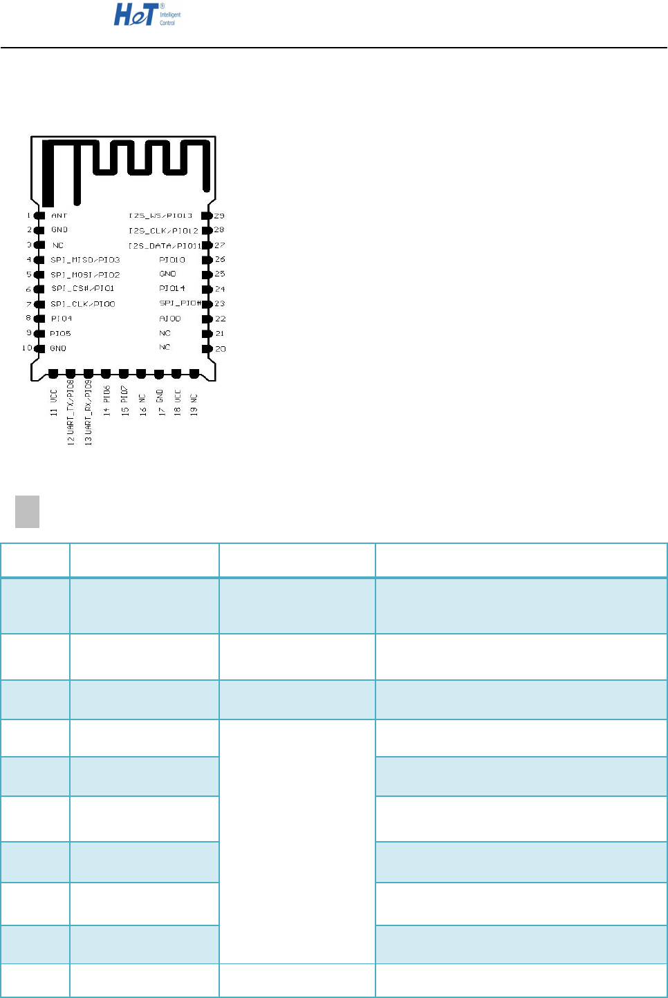
3. Interface Definition
3.1Pin Assignments
3.2Pin Description
PIN No.
PIN NAME
PIN TYPE
DESCRIPTION
1
ANT
External antenna
Antenna port for Bluetooth
transmitter / receiver.(can’t be used)
2
GND
Ground
Connect to GND
3
NC
Unused pins
Not connected
4
SPI_MISO/PIO3
Digital: Bidirectional with
programmable strength
internal
pull-up / pull-down and LCD
glass
driving capability
General programmable I/O line 3
5
SPI_MOSI/PIO2
General programmable I/O line 2
6
SPI_CS#/PIO1
General programmable I/O line 1
7
SPI_CLK/PIO0
General programmable I/O line 0
8
PIO4
General programmable I/O line 4
9
PIO5
General programmable I/O line 5
10
GND
Ground
Connect to GND

Shenzhen H&T Intelligent Control Co., Ltd
Proprietary Information, No Dissemination or Use Allowed Without Prior Written Permission. All printed copies are considered Uncontrolled copies
unless the copies are stamped with “Controlled Copy” by Documentation Control.
11
VCC
3V3
power-supply connection
12
UART_ TX/PIO8
Digital: Bidirectional
with
programmable strength
internal
pull-up / pull-down and
LCD glass
driving capability
General programmable I/O line 8
13
UART_ RX/PIO9
General programmable I/O line 9
14
PIO6
General programmable I/O line 6
15
PIO7
General programmable I/O line 7
16
NC
Unused pins
Not connected
17
GND
Ground
Connect to GND
18
VCC
3V3
power-supply connection
19
NC
Unused pins
Not connected
20
NC
Unused pins
Not connected
21
NC
Unused pins
Not connected
22
AIO0
Unidirectional analogue
Analogue programmable input
line
23
SPI_PIO#
Input with strong
internal Pull-down
Selects Debug SPI on PIO[3:0]
24
PIO14
Digital: Bidirectional
with
programmable strength
internal
pull-up / pull-down and
LCD glass
driving capability
General programmable I/O line 14
25
GND
Ground
Connect to GND
26
PIO10
Digital: Bidirectional
with
programmable strength
internal
pull-up / pull-down and
LCD glass
driving capability
General programmable I/O line 10
27
I2S_DATA/PIO11
General programmable I/O line 11
28
I2S_CLK/PIO12
General programmable I/O line 12
29
I2S_WS/PIO13
General programmable I/O line 13
Shenzhen H&T Intelligent Control Co., Ltd
Proprietary Information, No Dissemination or Use Allowed Without Prior Written Permission. All printed copies are considered Uncontrolled copies
unless the copies are stamped with “Controlled Copy” by Documentation Control.
4.Electrical Parameters
4.1 Maximum Rating Parameter
Pressure beyond the "maximum evaluation value" data will cause permanent damage to the device
unrecoverable. The following assessment is limited to the pressure, to go beyond the operations
specifications paragraph indicated functional operation will not apply to the following data. Under
absolute maximum evaluation value status will have an impact on long ‐term use of equipment
performance reliability.
Item
Min
Type
Max
Unit
Storage temperature
-40
-
85
℃
Battery (VDD_BAT and VDD_PADS)
0
-
3.6
V
I/O supply voltage
0
-
3.6
V
VDD_AUX, VDD_DIG, AIOs
0
-
1.26
V
VDD_RAD, VDD_RF_IN, VDD_RF
0
-
2.2
V
ESD
Human Body Model Contact Discharge per
JEDEC EIA /JS-001-2014
2
KV
Charged Device Model Contact Discharge
per JEDEC EIA /JS002-2014
500
V
4.2 Recommended Operation Conditions.
Item
Min
Type
Max
Unit
Operating temperature range
-30
20
85
℃
Battery (VDD_BAT) operation
1.4
3.0
3.6
V
I/O supply voltage (VDD_PADS)
1.4
3.0
3.6
V
4.3 Electronic Characteristics
Mode
Description
Total Typical
Current at 3 V

Shenzhen H&T Intelligent Control Co., Ltd
Proprietary Information, No Dissemination or Use Allowed Without Prior Written Permission. All printed copies are considered Uncontrolled copies
unless the copies are stamped with “Controlled Copy” by Documentation Control.
Deep Sleep: No RAM Retention and
External Interrupts Enabled
All functions are shut down.
To wake the chip, toggle a pre-configured PIO
1.6μA
Deep Sleep: No RAM Retention with
External Interrupts and Timer Enabled
VDD_PADS = ON
5.5μA
VDD_BAT = ON
Deep Sleep: 16 KB Data RAM Retention
VDD_PADS = ON
VDD_BAT =
ON
RAM = ON
10.5μA
Digital Circuits = ON
SMPS = ON
Deep Sleep: 16 KB Data RAM and 64
KB
RAM Retention
VDD_PADS = ON
VDD_BAT =
ON
RAM = ON
12μA
Digital Circuits = ON
SMPS = ON
Idle: Shallow Sleep
<1 :s Wake up Time
VDD_BAT =
ON
RAM = ON
0.75 mA
Digital Circuits = ON
MCU = IDLE
VDD_PADS= ON
Idle: Active
<1 :s Wake up Time
VDD_BAT =
ON
RAM = ON
1.3mA(Execution
from Cache)
Digital Circuits = ON
MCU = IDLE
VDD_PADS= ON
13.5 mA (Active
SMEM
Execution)
TX Active
4dBm Transmit Power
5 mA Average
RX Active
-90.5dBm Sensitivity
5 mA Average
4.4Input/Output Terminal Characteristics
Switch-mode Regulator
Min
Typ
Max
Unit
Output voltage (VDD_AUX)
-
1.2
-
V
Output voltage (VDD_DIG)
-
1.1
-
V
Output voltage (VDD_RAD)
-
1.8
-
V
Output voltage (VDD_MEM)
-
3.3
-
V
NOTE : These are internal regulators and should have no additional load connected.
Digital I/O Terminals
Input Voltage Levels
Min
Typ
Max
Unit

Shenzhen H&T Intelligent Control Co., Ltd
Proprietary Information, No Dissemination or Use Allowed Without Prior Written Permission. All printed copies are considered Uncontrolled copies
unless the copies are stamped with “Controlled Copy” by Documentation Control.
VIL input logic level low
-
-
25%xVDD_PADS
V
VIH input logic level high
75%xVDD_PADS
-
-
V
Output Voltage Levels
VOL output logic level low, IOL = 8.0 mA (Max Drive
Strength)
-
-
20%xVDD_PADS
V
VOH output logic level high, IOL = -8.0 mA (Max Drive
Strength)
80%xVDD_PADS
-
-
V
Tr/Tf (for 30 pF load)
-
-
2
ns
Input and Tristate
With strong pull-up
3.5
4.7
6.0
kΩ
With strong pull-down
3.5
4.7
6.0
kΩ
With weak pull-up
8
40
50
uA
With weak pull-down
10
40
50
uA
CI input capacitance
-
5
-
pF
NOTE Range applicable for VDD_PADS between 1.8 V and 3.3 V when measured as a short circuit.
AIO
Input/Output Voltage Levels
Min
Typ
Max
Unit
Input voltage
0
-
VDD_AUX
V
10-bit Aux ADC
10-bit Aux ADC
Min
Typ
Max
Unit
Resolution
-
-
10
Bits
Input voltage range(1)
0
-
VDD_AUX
V
Input bandwidth
-
100
-
kHz
Conversion time
1.38
1.68
4.14
us
Sample rate(2)
-
-
700
Samples/s
NOTE :1. LSB size = VDD_AUX/1023.
2. The 10-bit Aux ADC is accessed through the firmware API. The sample rate given is achieved as part
of this function.
Shenzhen H&T Intelligent Control Co., Ltd
Proprietary Information, No Dissemination or Use Allowed Without Prior Written Permission. All printed copies are considered Uncontrolled copies
unless the copies are stamped with “Controlled Copy” by Documentation Control.
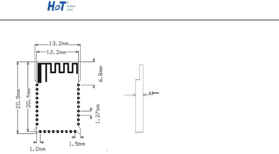
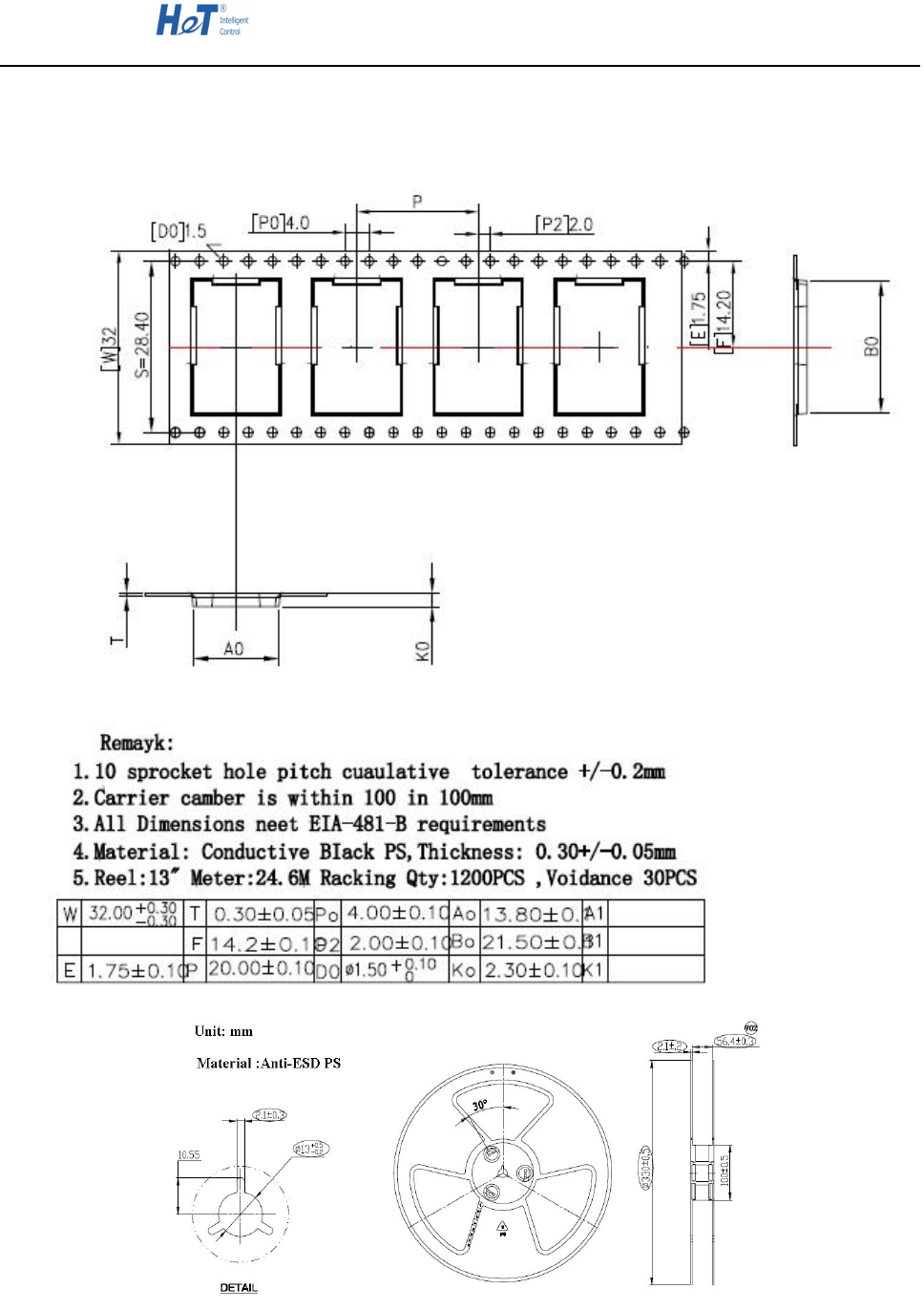
4. Module Mechanical Dimension
5. HET UART pass through Firmware functions Operating Instructions
5.1 Transparent Mode and Command Mode
Module can operate in transparent mode and command mode.
Transparent mode: In this mode, users don’t need to think about the complex Bluetooth
protocol application, you can complete the development of products quickly. In this mode the
module will automatically transmit the received UART data to the bonding mobile device through
Bluetooth. also it will automatically transmit the received Bluetooth data to the MCU through
UART. For product development, the user is responsible for the main MCU firmware design and
intelligent mobile device APP design.
Command Mode:In this mode, the module can be controlled through specific serial AT
commands, for details please refer “H&T BLE Modules Programming Guide”
5.2 Switch between two modes
The module can be switched between 2 modes through PIO7,when PIO7 is low, Command
Mode is enabled, when PIO7 is high, Transparent Mode is enabled.
5.3 Sleep and Wake
Before sending serial data to the module through UART, the PIO1 need to be pulled down to
Shenzhen H&T Intelligent Control Co., Ltd
Proprietary Information, No Dissemination or Use Allowed Without Prior Written Permission. All printed copies are considered Uncontrolled copies
unless the copies are stamped with “Controlled Copy” by Documentation Control.
wake up the module. When the user’s MCU monitors the module PIO12 has been pulled down, this
means module has been successfully woken up, then the data can be sent at this time. during data
transmission, PIO1 must remain low, after data transmission is completed, the PIO1 pin need to be
pulled up, then the module goes to sleep again to reduce power consumption.
Once the module receives data from another end BLE device, the data will be automatically
forwarded to the MCU, also the PIO10 pin will be pulled low to inform the MCU to receive data.
During data transmission PIO10 pin will remain low. After all serial data transmission is completed,
PIO10 pin will be pulled up.
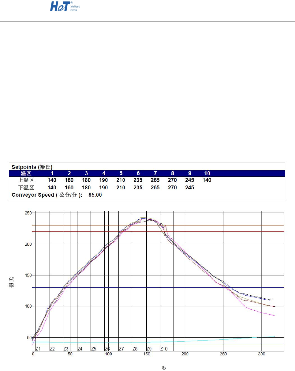
6. Temperature Profile of Reflow Soldering Process
7.Module Package Information
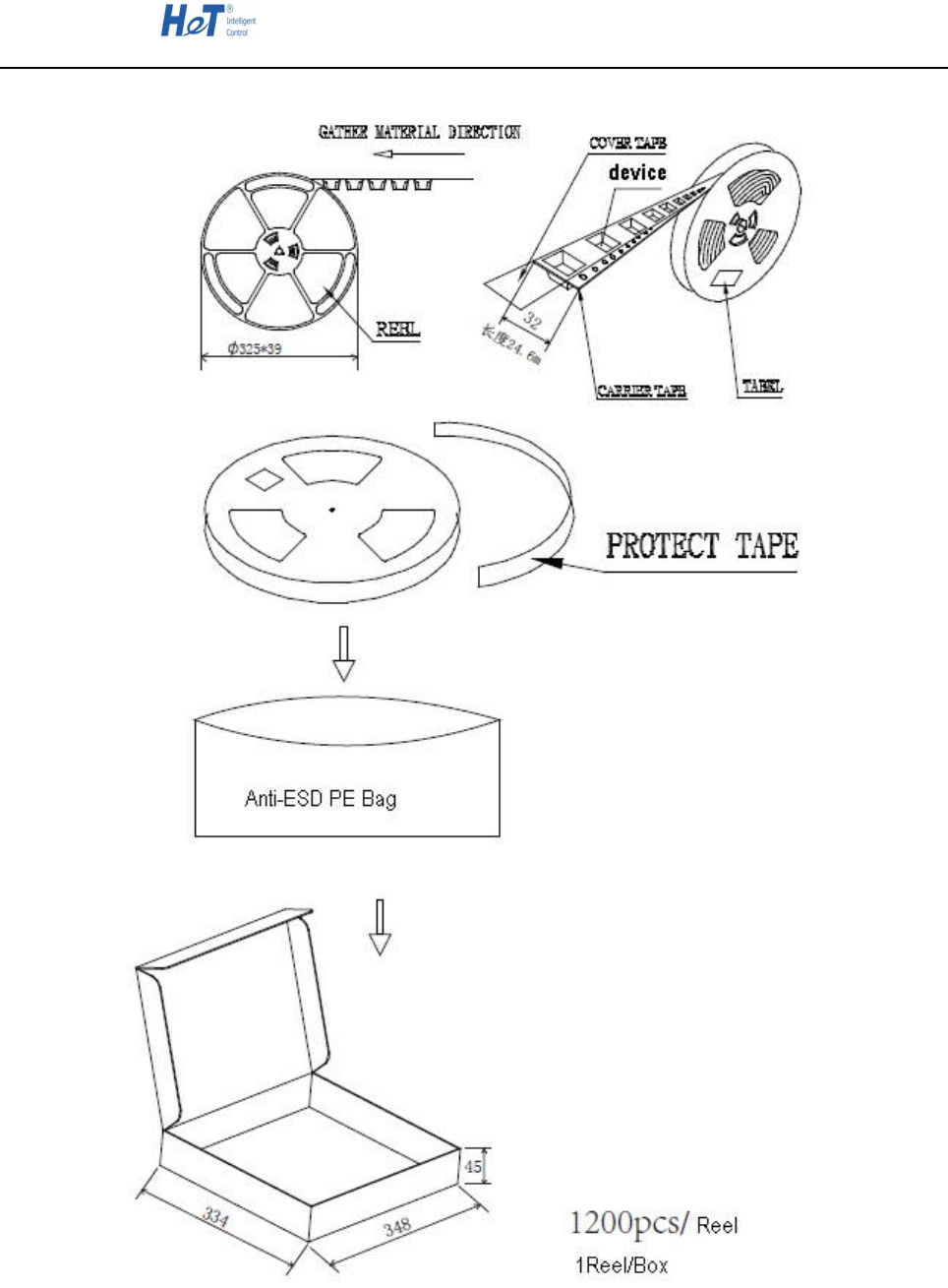
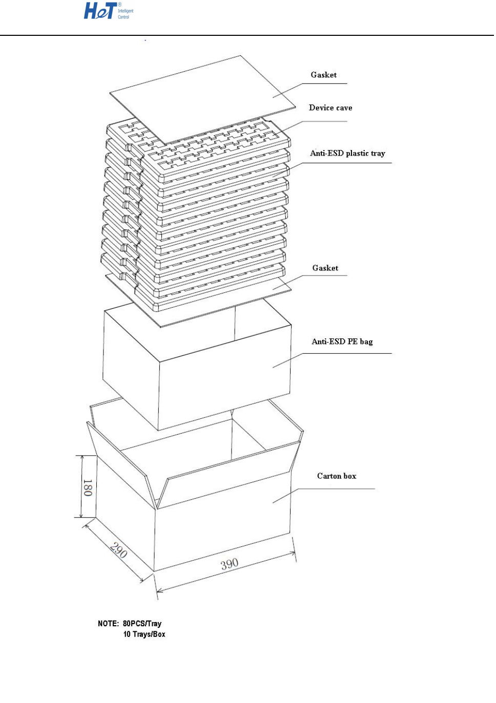
This module can be packaged with tape or tray after production, since this is ESD sensitive
device, precautions should be used when handling the device in order to prevent permanent
Shenzhen H&T Intelligent Control Co., Ltd
Proprietary Information, No Dissemination or Use Allowed Without Prior Written Permission. All printed copies are considered Uncontrolled copies
unless the copies are stamped with “Controlled Copy” by Documentation Control.
damage.
Below is the dimension of the packaging tape and reel:
Below is the tape packaging process:
Shenzhen H&T Intelligent Control Co., Ltd
Proprietary Information, No Dissemination or Use Allowed Without Prior Written Permission. All printed copies are considered Uncontrolled copies
unless the copies are stamped with “Controlled Copy” by Documentation Control.
Below is the tray packaging process:
Shenzhen H&T Intelligent Control Co., Ltd
Proprietary Information, No Dissemination or Use Allowed Without Prior Written Permission. All printed copies are considered Uncontrolled copies
unless the copies are stamped with “Controlled Copy” by Documentation Control.
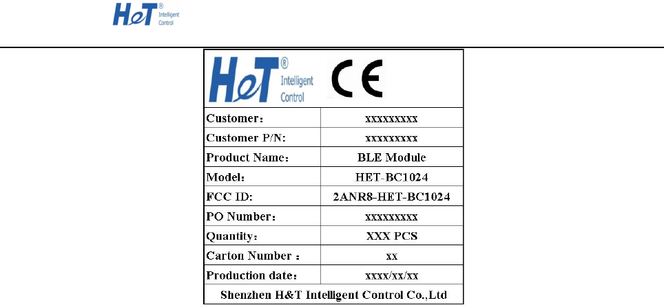
Below is the carton label drawing.
Shenzhen H&T Intelligent Control Co., Ltd
Proprietary Information, No Dissemination or Use Allowed Without Prior Written Permission. All printed copies are considered Uncontrolled copies
unless the copies are stamped with “Controlled Copy” by Documentation Control.

Shenzhen H&T Intelligent Control Co., Ltd
Proprietary Information, No Dissemination or Use Allowed Without Prior Written Permission. All printed copies are considered Uncontrolled copies
unless the copies are stamped with “Controlled Copy” by Documentation Control.
FCC Statement
15.19
1. This device complies with Part 15 of the FCC Rules. Operation is subject to the following two
conditions:
(1) This device may not cause harmful interference.
(2) This device must accept any interference received, including interference that may cause
undesired operation.
15.21
Note: The grantee is not responsible for any changes or modifications not expressly approved by the
party responsible for compliance. Such modifications could void the user’s authority to operate the
equipment.
15.105(b)
NOTE: This equipment has been tested and found to comply with the limits for a Class B digital
device, pursuant to part 15 of the FCC Rules. These limits are designed to provide reasonable
protection against harmful interference in a residential installation.
This equipment generates uses and can radiate radio frequency energy and, if not installed and used
in accordance with the instructions, may cause harmful interference to radio communications.
However, there is no guarantee that interference will not occur in a particular installation. If this
equipment does cause harmful interference to radio or television reception, which can be
determined by turning the equipment off and on, the user is encouraged to try to correct the
interference by one or more of the following measures:
- Reorient or relocate the receiving antenna.
- Increase the separation between the equipment and receiver.
-Connect the equipment into an outlet on a circuit different from that to which the receiver is
connected.
-Consult the dealer or an experienced radio/TV technician for help
RF Exposure Statement

Shenzhen H&T Intelligent Control Co., Ltd
Proprietary Information, No Dissemination or Use Allowed Without Prior Written Permission. All printed copies are considered Uncontrolled copies
unless the copies are stamped with “Controlled Copy” by Documentation Control.
This equipment complies with FCC radiation exposure limits set forth for an uncontrolled
environment. This equipment should be installed and operated with minimum distance of 5 mm
between the radiator and your body.
ORIGINAL EQUIPMENT MANUFACTURER (OEM) NOTES §
The OEM must certify the final end product to comply with unintentional radiators (FCC Sections 1
5.107 and 15.109) before declaring compliance of the final product to Part 15 of the FCC rules and r
egulations. Integration into devices that are directly or indirectly connected to AC lines must add wi
th Class II Permissive Change. §
The OEM must comply with the FCC labeling requirements. If the module’
s label is not visible when installed, then an additional permanent label must be applied on the outsi
de of the finished product which states: “Contains transmitter module FCC ID: 2ANR8-HET-BC10
24”. Additionally, the following statement should be included on the label and in the final product’
s user manual:“This device complies with Part 15 of the FCC Rules. Operation is subject to the foll
owing two conditions: (1) This device may not cause harmful interferences, and (2) this device must
accept any interference received, including interference that may cause undesired operation.”
This Module is full modular approval, it is limited to OEM installation ONLY.