HON HAI PRECISION IND T77H566 WiFi/BT Module User Manual 802
HON HAI Precision Ind. Co., Ltd. WiFi/BT Module 802
User Manual rev.pdf

COMPANY CONFIDENTIAL
Preliminary Datasheet
1
BCM4356 Dual-Band 2x2 802.11ac and Bluetooth v4.1
Combo Module
Project Name
M.2 Type1216 BCM4356
WLAN + BT Combo Module
Foxconn Part No.
T77H566.01
Customer Model Name.
PK29S005P10
Product Revision
01S1
HON HAI PRECISION IND. CO., LTD.
No.2, 2nd Dong Huan Road, 10th
YouSong lndustrial District, Longhua
Town, Baoan, ShenZhen
Tel: +86-755-28128988#29413
Fax: +86-755-28129800#64886
Revision Note
WiFi/BT Module
WiFi/BT Module

COMPANY CONFIDENTIAL
Preliminary Datasheet
2
Index
1. REVISION HISTORY ................................................................................................................................................... 3
2. INTRODUCTION .......................................................................................................................................................... 4
2.1 HARDWARE ARCHITECTURE .................................................................................................................................... 4
2.2 FEATURES ................................................................................................................................................................ 5
2.3 STANDARDS COMPLIANCE ....................................................................................................................................... 5
3. MECHANICAL SPECIFICATION .............................................................................................................................. 6
3.1 MECHANICAL DRAWING ............................................................................................................................................ 6
3.2 PCB STACK .............................................................................................................................................................. 6
3.3 RECOMMENDED LGA LAND PATTERN ..................................................................................................................... 7
3.4 RECOMMENDED STENCIL APERTURE ....................................................................................................................... 7
3.5 RF CONNECTOR TYPE ............................................................................................................................................. 8
3.6 RF CABLE ASSEMBLY NOTICE .................................................................................................................................. 9
3.7 RF PORT DEFINE ...................................................................................................................................................... 9
4. LGA PIN-OUT DEFINITION ..................................................................................................................................... 10
4.1 MODULE PIN-OUT DEFINITION ................................................................................................................................. 10
4.2 PIN DEFINITION ....................................................................................................................................................... 11
5. PRODUCT SPECIFICATION ................................................................................................................................... 13
5.1 DC ELECTRICAL SPECIFICATION ........................................................................................................................... 13
5.2 RF CHARACTERISTICS(TBD) ................................................................................................................................. 13
5.3 POWER UP SEQUENCE AND TIMING ...................................................................................................................... 15
5.3.1 Control signal Timing (WLAN=ON, BT=ON) ........................................................................................... 16
5.3.2 Control signal Timing (WLAN=OFF, BT=OFF) ....................................................................................... 16
5.3.3 Control signal Timing (WLAN=ON, BT=OFF) ......................................................................................... 17
5.3.3 Control signal Timing (WLAN=OFF, BT=ON) ......................................................................................... 17
5.3.4 WLAN Boot Up Sequence .......................................................................................................................... 17
5.4 UART HOST INTERFACE TIMING ........................................................................................................................... 18
5.5 PCM INTERFACE TIMING ....................................................................................................................................... 19
6.SCHEMATIC REFERENCE DESIGN ...................................................................................................................... 24
7. SOFTWARE REQUIREMENT(TBD) ....................................................................................................................... 26
8. REGULATORY(TBD) ................................................................................................................................................ 26
9. QUALITY ..................................................................................................................................................................... 26
10. PACKAGE INFORMATION ................................................................................................................................... 27
11. ENVIRONMENTAL REQUIREMENTS AND SPECIFICATIONS ..................................................................... 28
11.1 TEMPERATURE ..................................................................................................................................................... 28
11.2 PCB BENDING ...................................................................................................................................................... 28
11.3 HANDLING ENVIRONMENT .................................................................................................................................... 28
11.4 STORAGE CONDITION .......................................................................................................................................... 28
11.5 BAKING CONDITION .............................................................................................................................................. 28
11.6 SOLDERING AND REFLOW CONDITION .................................................................................................................. 29

COMPANY CONFIDENTIAL
Preliminary Datasheet
3
1. Revision History
Date
Change Note
Author
REV Note
2014-07-25
Initial release(draft)
Robin Xu
0.1
2014-07-30
Add customer project code
Robin Xu
0.2
2014-08-21
1.Update the block diagram and support BTv4.1 in section2
2.Update the ME drawing in section3.1
3.Update the Recommended stencil aperture in setion3.4
Robin Xu
0.3
2014-11-14
Update WiFi Transmit Output Power
Ru-yan Li
0.4
2014-12-2
Add 3.7 RF port define
Ru-yan Li
0.5
2014-12-25
1.Update WLAN host interface description
2.Update BT RX sensitivity level
Ru-yan Li
0.6
COMPANY CONFIDENTIAL
Preliminary Datasheet
4
2. Introduction
Project Name: M.2 Type 1216 BCM4356 WLAN+BT Combo Module
Project Number: T77H566.01
Form factor
M.2 Type 1216 LGA
Host Interface
WLAN: PCIe mode complies with PCI Express
base specification revision 3.0 for x1 lane and
power management running at Gen1 speeds.
BT: UART for data, PCM for audio
PCB
6-layer HDI design
RF connector
Two MHF-4 RF connectors on module
This documentation describes the engineering requirements specification of this M.2 1216 type module.
WLAN is compliant with IEEE 802.11 a/b/g/n and 2x2 IEEE 802.11ac MAC/ baseband/radio, Bluetooth is
compliant with Bluetooth v4.1+HS. This module takes advantage of the high throughput and extended range
of Broadcom MIMO solution It is a confidential document of Foxconn.
* For b/g/n and a/b/g/n module, Foxconn HW/FW is the same, platform use different firmware and driver
to enable or disable 5GHz 11ac function.
2.1 Hardware Architecture
The WLAN+BT combo module is designed base on BROADCOM BCM4356 chipset with external LNA for
both 2.4G and 5GHz. The BCM4356 is a complete dual-band (2.4GHz and 5GHz) Wi-Fi 2X2 MIMO
MAC/PHY/Radio System-on-a-Chip. This Wi-Fi single–chip device provides a high level of integration with
dual-stream IEEE 802.11ac MAC/baseband/radio, Bluetooth v4.1 + HS. In IEEE802.11ac mode, the WLAN
operation supports rates of MCS0-MCS9 (up to 256QAM) in 20MHz, 40MHz and 80MHz channels for data
rates up to 866.7Mbps. In addition, all the rates specified in IEEE802.11a/b/g/n are supported. See the
block diagram as below:
WiFi/BT Module

COMPANY CONFIDENTIAL
Preliminary Datasheet
5
2.2 Features
This module supports the following features:
IEEE 802.11a/b/g/n/ac dual-band 2x2 MIMO radio with virtual-simultaneous dual-band operation
Bluetooth v4.1+EDR with integrated class1 PA
Enhanced Bluetooth and WLAN coexistence performance
WLAN PCIe module complies with PCI express base specification for x1 lane and power management
running at Gen1 speeds.
Integrated ARMCR4TM processor with tightly coupled memory for complete WLAN subsystem
functionality minimizing the need to wake up the applications processor for standard WLAN functions.
This allows for further minimization of power consumption, while maintaining the ability to field upgrade
with features,
On-chip memory includes 768KB SRAM and 640KB ROM.
OneDriverTM software architecture for easy migration from existing embedded WLAN and Bluetooth
devices as well as future devices.
TX and RX low-density parity check (LDPC) support for improved range and power efficiency.
Supports IEEE802.11ac/n beam forming.
Bluetooth supports a high–speed UART interface(up to 4Mbps) and PCM for audio
Bluetooth Smart Audio technology improves voice and music quality to headsets
Bluetooth low power inquiry and page scan
Bluetooth low energy(BLE) support
Bluetooth Packet Loss Concealment(PLC)
Bluetooth Wide Band Speech(WBS)
GP/HF compliance
2.3 Standards Compliance
Bluetooth 2.1+EDR
Bluetooth 3.0+HS
Bluetooth 4.1(Bluetooth Low Energy)
IEEE802.11ac mandatory and optional requirements for 20MHz,40MHz and 80MHz channels
IEEE802.11n
IEEE802.11a
IEEE802.11b
IEEE802.11g
IEEE802.11d
IEEE802.11h
IEEE802.11i
Security
- WEP
- WPA/WPA2
- WMM/WMM-PS(U-APSD)/WMM-SA
- AES(Hardware Accelerator)
- TKIP(Hardware Accelerator)
- CKIP(SW support)
Proprietary Protocols
- CCXv2
- CCXv3
- CCXv4
- CCXv5
IEEE802.15.2 coexistence compliance-on silicon solution compliant with IEEE 3wire requirements
The module will the following future draft/standards:
IEEE802.11r-Fast Roaming (between APs)
IEEE802.11w-Secure Management Frames
IEEE802.11 Extensions:
- IEEE802.11e QoS Enhancements(In accordance with the WMM spec, QoS is already supported)
- IEEE802.11h 5GHz Extensions
- IEEE802.11i MAC Enhancements
- IEEE802.11k Radio Resource Measurement
COMPANY CONFIDENTIAL
Preliminary Datasheet
6
3. Mechanical Specification
3.1 Mechanical Drawing
Typical module dimension (W x L): 12mmx16mm. Max Z-height is 1.53mm.
Unit:mm
3.2 PCB stack
6 Layers, HDI, thickness:0.43mm +/-0.05mm
COMPANY CONFIDENTIAL
Preliminary Datasheet
7
3.3 Recommended LGA Land Pattern
Unit: mm
TOP VIEW
Suggest use “solder-mask on pad” design for main-board to avoid the soldering short.
3.4 Recommended stencil aperture
Remark: Red stencil layer Green (pad layer)
Below is recommendation about respectively defined apertures as A,B,B`,C and C`
Stencil thickness=0.12mm
A=24*24 mil2 B=22*9 mil2 B`=24*9 mil2 C=40*40 mil2 C`=29.5*29.5mil2
Define space between apertures as D and E
D=11mil E=19.5mil
COMPANY CONFIDENTIAL
Preliminary Datasheet
8
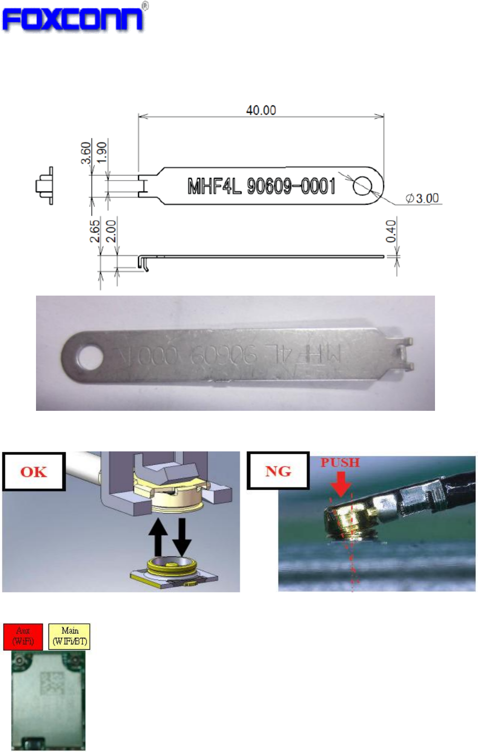
3.5 RF Connector Type
The standard 2x2mm size RF receptacle connectors to be used in conjunction with the M.2
boards/modules
Same RF Receptacle on module supports either 0.81mm or 1.13mm diameter cable
Prefer to use 1.13mm diameter cable for lower cable loss
1.2mm max. mated height for low profile design
Example of IPEX RF connector
IPEX P/N: 20449-001E (MHF-4)
Antenna Placement
Antenna
Interface
Remark
ANT1
WLAN/BT
Main
ANT2
WLAN
AUX
COMPANY CONFIDENTIAL
Preliminary Datasheet
9
3.6 RF cable assembly notice
1> Mating/Unmating Jig
We recommend to use below Jig for mating/Unmating RF cable
2> Mating method of RF cable
Please push as gently as possible while mating plug with receptacle.
(The force must be 30N Max.)
3.7 RF port define
Main ANT for WiFi and BT, Aux ANT for WiFi.
COMPANY CONFIDENTIAL
Preliminary Datasheet
10
4. LGA Pin-out Definition
4.1 Module pin-out definition
96
95
94
93
92
91
90
89
88
87
86
85
84
83
82
81
80
79
78
77
105
GND
GND
GND
GND
GND
GND
GND
GND
GND
GND
GND
GND
GND
GND
GND
GND
GND
GND
GND
GND
GND
GND
108
1
NC
GND
76
2
NC
GND
75
3
NC
GND
74
4
3.3V
GND
GND
3.3V
73
5
3.3V
97
104
3.3V
72
6
GND
GND
71
7
NC
BT_USB_DP
70
8
NC
BT_USB_DN
69
9
NC
GND
68
10
NC
GND
GND
NC
67
11
NC
98
103
NC
66
12
NC
WLAN_LED_L
65
13
NC
BT_LED_L
64
14
NC
BT_REG_ON
63
15
NC
GND
62
16
NC
GND
GND
BT_PCM_CLK
61
17
GND
99
102
BT_PCM_OUT
60
18
NC
BT_PCM_IN
59
19
NC
BT_PCM_SYNC
58
20
GND
BT_UART_RTS_L
57
21
NC
BT_UART_RXD
56
22
NC
GND
GND
BT_UART_TXD
55
23
GND
100
101
BT_UART_CTS_L
54
24
BT_DEV_WAKE
BT_UART_HOST_
WAKE_L
53
25
NC
SDIO_CLK
52
26
GND
SDIO_CMD
51
27
SUSCLK(32KHz)
SDIO_DATA0
50
28
WL_RFDISABLE_L
SDIO_DATA1
49
106
GND
PCIE_PME_L
PCIE_CLKREQ_L
PCIE_PERST_L
GND
PCIE_REFCLKN
PCIE_REFCLKP
GND
PCIE_TDN
PCIE_TDP
GND
PCIE_RDN
PCIE_RDP
GND
VIO
NC
NC
WL_REG_ON
SDIO_WAKE_L
SDIO_DATA3
SDIO_DATA2
GND
107
29
30
31
32
33
34
35
36
37
38
39
40
41
42
43
44
45
46
47
48
Top view

COMPANY CONFIDENTIAL
Preliminary Datasheet
11
4.2 Pin definition
Pin No.
Pin Name
Type
Description
Voltage
Conne
cting
1-3, 7-16,
18,19,21,
22,25,
43-44,66,
67
NC
-
No connection
-
No
4,5,72,73
3.3V
Power
DC 3.3V power input
3.3V
Yes
24
BT_DEV_WAKE
I
Bluetooth device wake-up: Signal from the
host to the BCM4356 indicating that the host
requires attention.
• Asserted: The Bluetooth device must
wake-up or remain
awake.
• Deasserted: The Bluetooth device may
sleep when sleep criteria are met. The
polarity of this signal is software
configurable and can be asserted high or
low.
1.8V
Yes
27
SUSCLK (32KHz)
I
Suspend Clock is a 32.768 kHz clock supply
input that is provided by platform to enable
the add-in card to enter reduce power
consumption modes. SUSCLK will have a
duty cycle that can be as low as 30% or as
high as 70%. Accuracy will be up to
200ppm. See the detail spec in section6.
1.8V
(Note1)
Yes
28
WLAN_RFDISAB
LE_L
I
Active low, debounced signal when applied
by the system it will disable WLAN radio
operation on the add-in cards that implement
radio frequency applications. This signal is
internal pull-up on the card by default.
1.8V
(Note2)
No
29
PCIE_PME_L
OD
PCIe PME Wake. Open Drain with pull up on
platform; Active Low
1.8V
Yes
30
PCIE_CLKREQ_
L
OD
Clock Request is a reference clock request
signal as defined by the PCIe Mini Card CEM
specification; Also used by L1 PM Substates.
1.8V
Yes
31
PCIE_PERST_L
I
PE-Reset is a functional reset to the Add-In
card as defined by the PCIe Mini Card CEM
specification
1.8V
Yes
33
PCIE_REFCLKN
I
PCIe Reference Clock signals (100 MHz)
defined by the PCIe specification.
-
Yes
34
PCIE_REFCLKP
36
PCIE_TDN
O
PCIe TX differential signals defined by the
PCIe specification
-
Yes
37
PCIE_TDP
39
PCIE_RDN
I
PCIe RX differential signals defined by the
PCIe specification. Add AC cap 0.1uF on
PCIe signals of host side.
-
Yes
40
PCIE_RDP
42
VIO
Power
Reserved for external 1.8V power source
input. If don’t need, MUST keep it floating or
open
1.8V
(Note3)
Option
45
WL_REG_ON
I
SDIO sideband GPIO pin to enable/disable
(reset) the WiFi function. Platform firmware is
required to assert/de-assert this pin on every
boot (warm and cold). High active. See the
detail sequence timing in section5.3.
1.8V
Yes
46
SDIO_WAKE_L
O
SDIO Host Wake. Note in band SDIO wake is
not used for non-active modes, Active Low.
Require pull up on the host side
( recommended 15K to 100K )
1.8V
No

COMPANY CONFIDENTIAL
Preliminary Datasheet
12
47
SDIO_DATA3
I/O
SDIO data line 3
1.8V
No
48
SDIO_DATA2
I/O
SDIO data line 2
1.8V
No
49
SDIO_DATA1
I/O
SDIO data line 1
1.8V
No
50
SDIO_DATA0
I/O
SDIO data line 0
1.8V
No
51
SDIO_CMD
I/O
SDIO Command line
1.8V
No
52
SDIO_CLK
I
SDIO clock input
1.8V
No
53
BT_UART_HOST
_WAKE_L
O
UART sideband used to wake up host
platform via BT device.
Open Drain, Active Low. Require pull up on
the host side (recommended 15K to 100K )
1.8V
Yes
54
BT_UART_CTS_
L
I
UART Clear To Send connected to RTS on
the platform.
1.8V
Yes
55
BT_UART_TXD
O
UART Transmit Data connected to RXD on
the platform.
1.8V
Yes
56
BT_UART_RXD
I
UART Receive Data connected to TXD on
the platform.
1.8V
Yes
57
BT_UART_RTS_
L
O
UART Ready To Send connected to CTS on
the platform.
1.8V
Yes
58
BT_PCM_SYNC
I/O
PCM synchronous data SYNC/ I2S Word
Select.
1.8V
Yes
59
BT_PCM_IN
I
PCM synchronous data input/ I2S Serial Data
IN.
1.8V
Yes
60
BT_PCM_OUT
O
PCM synchronous data output/ I2S Serial
Data OUT
1.8V
Yes
61
BT_PCM_CLK
I/O
PCM Clock/ I2S Continuous Serial Clock
(SCK)
1.8V
Yes
63
BT_REG_ON
I
Active high. Use GPIO pin to enable/disable
the BT function.
1.8V
Yes
64
BT_LED_L
O
BT LED, open drain, active low signal. This
signal is used to allow the add-in card to
provide status indicators via LED devices that
will be provided by the system.
1.8V
Option
65
WL_LED_L
O
WLAN LED, open drain, active low signal.
This signal is used to allow the add-in card to
provide status indicators via LED devices that
will be provided by the system.
1.8V
Option
69
BT_USB_DN
I/O
USB Data ± Differential serial data interface
compliant to the USB 2.0 Specification
-
No
70
BT_USB _DP
6,17,20,
23,26,32,
35,38,41,
62,68,71,
74-108
GND
GND
Ground
0V
Yes
Note1: for pin27 SUSCLK(32KHz) signal, BCM4356 chipset is capable to tolerate 3.3V, but 1.8V input source is
recommended.
Note2: for pin28 WLAN_RFDISABLE signal, it is provided for legacy wireless communications add-in cards.
It allows users to disable the add-in card’s RF radio operation via a system-provided switch in order to meet public safety
regulations or when otherwise desired. The wireless disable signals are active low signals that when asserted (driven low)
by the system shall disable radio operation. All transients resulting from mechanical switches need to be de-bounced by
system circuitry. It is anticipated that in the future the requirement for hardware wireless disable signals will be
deprecated from use in favor of in-band mechanisms. If use SDIO interface, prefer to use pin45 to do software control to
implement enable/disable the WiFi function. Default is 1.8V, and is capable to tolerate 3.3V.
Note3: for pin42 VIO, by default, MUST keep this pin floating or open.
If host platform can provide the external 1.8V power source as module IO voltage input, thus, the LDO inside module can
be removed. It’s just for customized design only
COMPANY CONFIDENTIAL
Preliminary Datasheet
13
5. Product Specification
5.1 DC Electrical Specification
Absolute Maximum Ratings
These specifications indicate levels where permanent damage to the device can occur. Functional operation
is not guaranteed under these conditions. Operation at absolute maximum conditions for extended can
adversely affect long-term reliability of the device.
Recommended Operating Condition
Element
Symbol
Value
Unit
Minimum
Typical
Maximum
DC supply voltage for the device
3.3V
3.15
3.3
3.45
V
Function operation is not guaranteed outside this limit, and operation outside this limit for extended periods
can adversely affect long-term reliability of the device.
5.2 RF Characteristics(TBD)
All typical performance specification are measured at RF connector port based-on the room
temperature(+25℃) and nominal supply voltages
The performance will be updated later based-on overall EDVT and regulatory testing..
WLAN
Standard
IEEE802.11a/b/g/n/ac
Data Rate
2.4GHz
802.11b: 11, 5.5, 2, 1 Mbps;
802.11g: 54, 48, 36, 24, 18, 12, 9, 6 Mbps
802.11n:
HT20 mode: up to 144.4Mbps
5GHz
802.11a: 54, 48, 36, 24, 18, 12, 9, 6 Mbps
802.11n:
HT20 mode: MCS0~7,up to 144.4Mbps
HT40 mode: MCS0~7,up to 300Mbps
802.11ac VHT20: MCS0~8, up to 173.3Mbps
802.11ac VHT40: MCS0~9, up to 400Mbps
802.11ac VHT80: MCS0~9, up to 866.7Mbps
Modulation Techniques
802.11b: CCK, DQPSK, DBPSK
802.11a/g: 64QAM,16QAM, QPSK, BPSK
802.11n: 64QAM,16QAM, QPSK, BPSK
802.11ac: 256QAM,64QAM,16QAM, QPSK, BPSK
Frequency Range
2.4GHz~2.4835GHz
5.15GHz~5.845GHz
Media Access Control
CSMA/CA with ACK
Rating
Symbol
Value
Unit
DC supply voltage for the device
3.3V
-0.5 to 3.9
V

COMPANY CONFIDENTIAL
Preliminary Datasheet
14
Transmit Output Power
Per Each Chain
2.4GHz:
11b 1~11Mbps: 16+/-1.5dBm
11g 6~54Mbps: 15+/-1.5dBm
11n HT20 MCS0~ MCS7: 14+/-1.5dBm
5GHz:
11a 6~12Mbps: 15+/-1.5dBm
11a 18~54Mbps: 14+/-1.5dBm
11n/ac 20MHz MCS0~ MCS2: 15+/-1.5dBm
11n/ac 20MHz MCS3~ MCS7: 14+/-1.5dBm
11n/ac 40MHz MCS0~ MCS2: 15+/-1.5dBm
11n/ac 40MHz MCS3~ MCS6: 14+/-1.5dBm
11n/ac HT40 MCS7: 13+/-1.5dBm
11ac VHT20 MCS8: 11+/-1.5dBm
11ac VHT40 MCS8~ MCS9: 11+/-1.5dBm
11ac VHT80 MCS0~ MCS2: 14.5+/-1.5dBm
11ac VHT80 MCS3~ MCS6: 14+/-1.5dBm
11ac VHT80 MCS7: 12+/-1.5dBm
11ac VHT80 MCS8~MCS9: 10+/-1.5dBm
Typical Minimum Receiver
Sensitivity
Per Each Chain
2.4GHz:
11b 1Mbps: -94dBm@PER<=8%
11b 11Mbps: -86dBm@PER<=8%
11g 6Mbps: -90dBm@PER<=10%
11g 54Mbps: -72dBm@PER<=10%
11n HT20 MCS0: -89dBm@PER<=10%
11n HT20 MCS7: -68dBm@PER<=10%
5GHz:
11a 6Mbps: -90dBm@PER<=10%
11a 54Mbps: -72dBm@PER<=10%
11n HT20 MCS0: -90dBm@PER<=10%
11n HT20 MCS7: -69dBm@PER<=10%
11n HT40 MCS0: -86dBm@PER<=10%
11n HT40 MCS7: -67dBm@PER<=10%
11ac VHT20 MCS0,Nss1: -89dBm@PER<=10%
11ac VHT20 MCS8,Nss1: -66dBm@PER<=10%
11ac VHT40 MCS0,Nss1: -86dBm@PER<=10%
11ac VHT40 MCS9,Nss1: -62.5dBm@PER<=10%
11ac VHT80 MCS0,Nss1: -82dBm@PER<=10%
11ac VHT80 MCS9,Nss1: -58dBm@PER<=10%
BT
Radio Modulation Technology
FHSS
Operating Frequency
2.402GHz ~ 2.4835GHz
Channel Numbers
79 channels with 1MHz BW
BDR Transmitter Output
Power
Typical +9dBm for Class1 (TBD)
BDR Power Control
2dB≤Power Control Step≤8dB
BDR Initial Carrier Freq.
Tolerance
≤ ± 75 kHz
BDR Carrier Frequency Drift
Drift Rate/50us <±20kHz
DH1: +/- 25kHz
DH3: +/- 40kHz
DH5: +/- 40kHz
BDR Modulation
Characteristics
140kHz ≤ Δf1avg ≤175kHz
Δf2max ≥115kHz
Δf2avg/Δf1avg ≥0.8
BDR Maximum Receiver
Signal
-20dBm@BER < 0.1% at 1Mbps
BDR Multi-slot Sensitivity
-85dBm@BER < 0.1% at 1Mbps
BDR Single Sensitivity
-85dBm@BER <= 0.1% at 1Mbps

COMPANY CONFIDENTIAL
Preliminary Datasheet
15
EDR Relative Power
P[GFSK]-4dB<P[DPSK]< P[GFSK]+1dB
EDR Stability and Mod
Accuracy
-75 kHz <ωi < 75 kHz
-10kHz<ω0 <10kHz
RMS DEVM<=0.13 for all 8DPSK @3Mbps
Peak DEVM<=0.25 for all 8DPSK @3Mbps
99% DEVM<=0.2 for 99% 8DPSK @3Mbps
BDR Frequency Range
FL>2.4GHz,FH<2.4835GHz
EDR Sensitivity
-86dBm@BER <= 0.01% at 2Mbps
-79dBm@BER <= 0.01% at 3Mbps
BDR TX Output Spectrum
-20dB Bandwidth
≤1MHz
LE Output Power
<10dBm
LE Modulation
Characteristics
225kHz ≤ Δf1avg ≤275kHz;
Δf2max ≥185kHz for at least 99.9% test packets;
Δf2avg/Δf1avg ≥0.8
LE Carrier frequency offset
and drift
Carrier frequency offset: ±150kHz
Carrier Drift: ≤50kHz
Drift rate: ≤20kHz/50us
LE Receiver Sensitivity
-85dBm@PER <= 30.8%
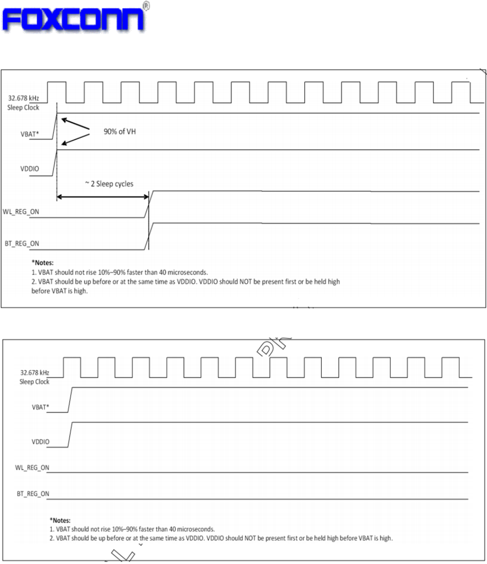
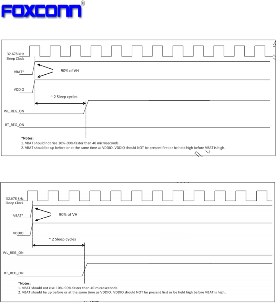
5.3 Power Up Sequence and Timing
The BCM4356 has two signals WL_REG_ON [pin45] & BT_REG_ON [pin63] that allows the host to control
the power consumption by enabling or disabling the Bluetooth, WLAN and internal regulator blocks. Below
timing diagram are provided to indicate proper sequencing of the signals for various operational states.
WL_REG_ON [pin45]
Used by the PMU to power up the WLAN section. It’s also OR-gated with BT_REG_ON input to control
the internal BCM4356 regulators. When this pin is high, the regulatory are enabled and the WLAN
section is out of reset. When this pin is low, the WLAN section is in reset. If both the BT_REG_ON and
WLAN_REG_ON pins are low, the regulators are disable.
BT_REG_ON [pin63]
Used by the PMU(OR-gated with WL_REG_ON) to power up the internal BCM4356 regulators. If both
the BT_REG_ON and WLAN_REG_ON pins are low, the regulators are disable. When this pin is high,
the regulatory are enabled and the BT section is out of reset. When this pin is low, the BT section is in
reset.
Remark: VBAT means DC input 3.3V in below timing diagram.
COMPANY CONFIDENTIAL
Preliminary Datasheet
16
5.3.1 Control signal Timing (WLAN=ON, BT=ON)
5.3.2 Control signal Timing (WLAN=OFF, BT=OFF)
COMPANY CONFIDENTIAL
Preliminary Datasheet
17
5.3.3 Control signal Timing (WLAN=ON, BT=OFF)
5.3.3 Control signal Timing (WLAN=OFF, BT=ON)
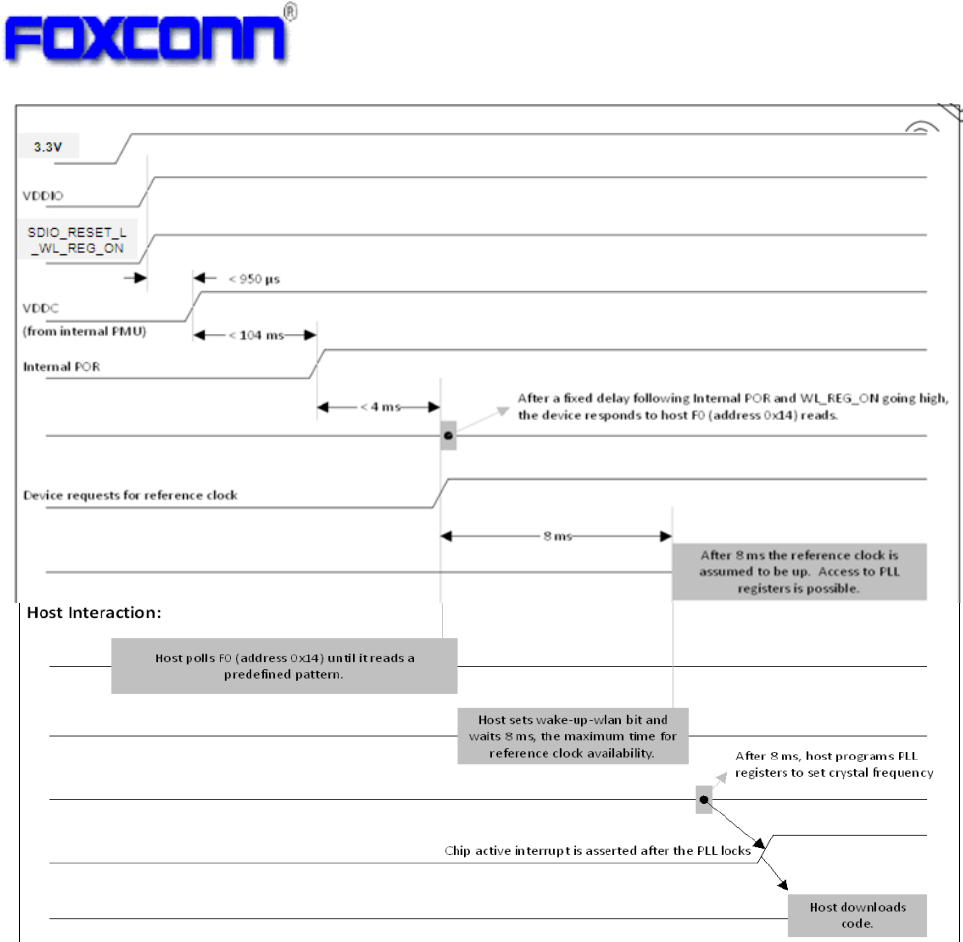
5.3.4 WLAN Boot Up Sequence
Below figure shows that the WLAN boot-up sequence from power-up to firmware download.
COMPANY CONFIDENTIAL
Preliminary Datasheet
18
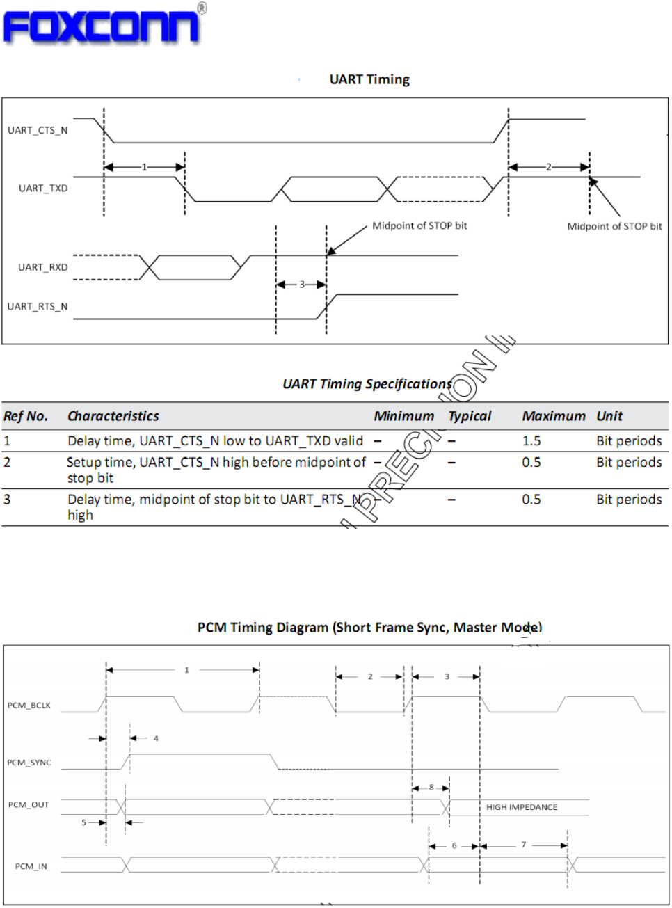
5.4 UART Host Interface Timing
The UART is a standard 4-wire interface(RX,TX,RTS and CTS) with adjustable baud rates
from 9600bps to 4.0Mbps.
COMPANY CONFIDENTIAL
Preliminary Datasheet
19
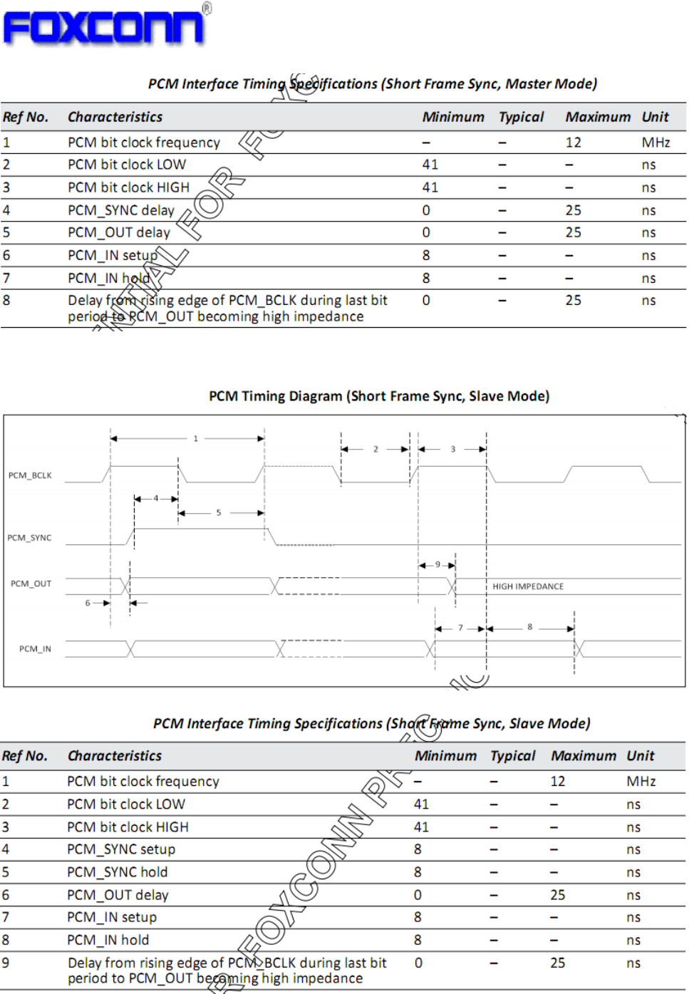
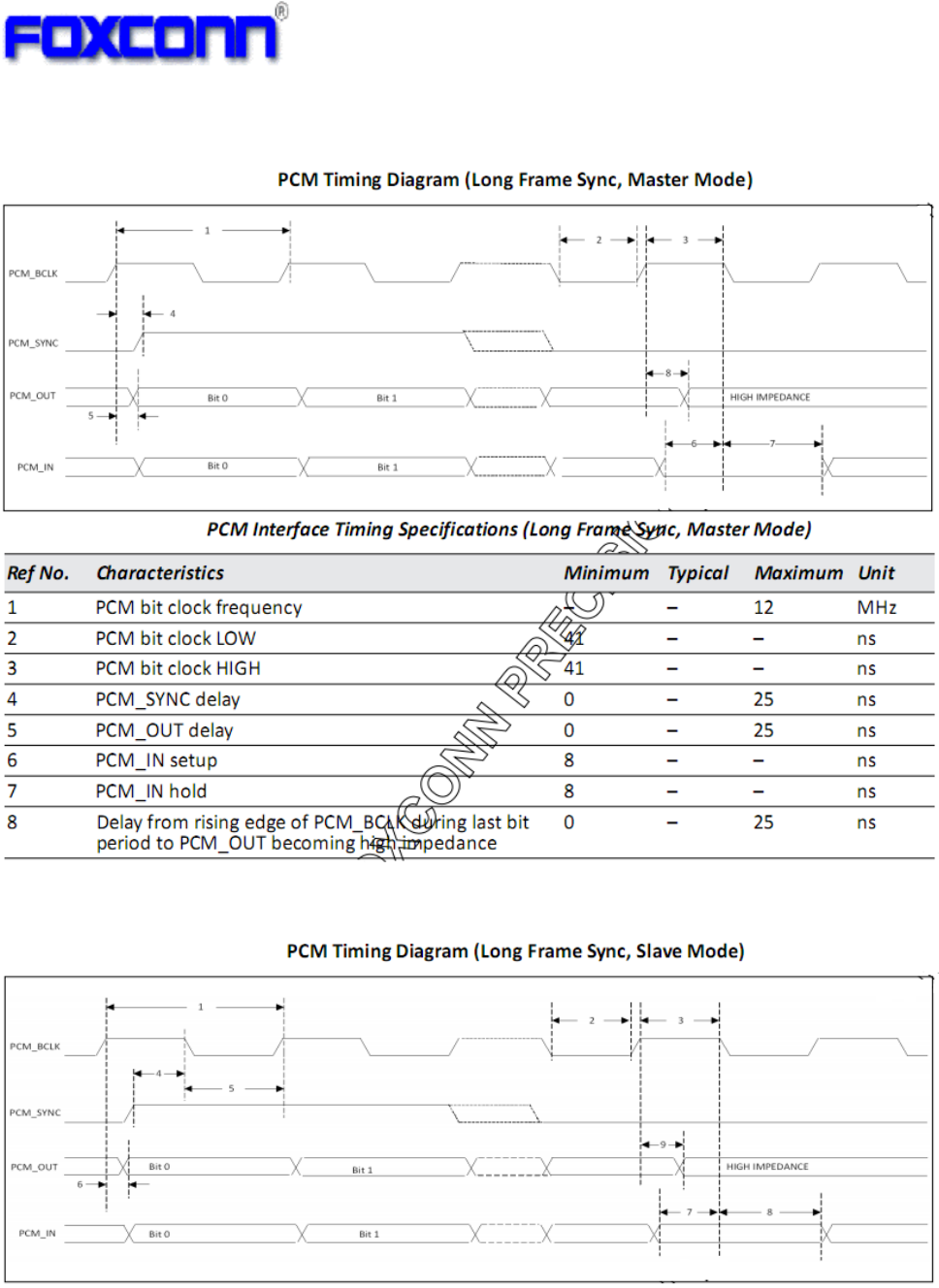
5.5 PCM Interface Timing
Short Frame Sync, Master Mode
COMPANY CONFIDENTIAL
Preliminary Datasheet
20
Short Frame Sync, Slave Mode
COMPANY CONFIDENTIAL
Preliminary Datasheet
21
Long Frame Sync, Master Mode
Long Frame Sync, Slave Mode
COMPANY CONFIDENTIAL
Preliminary Datasheet
22
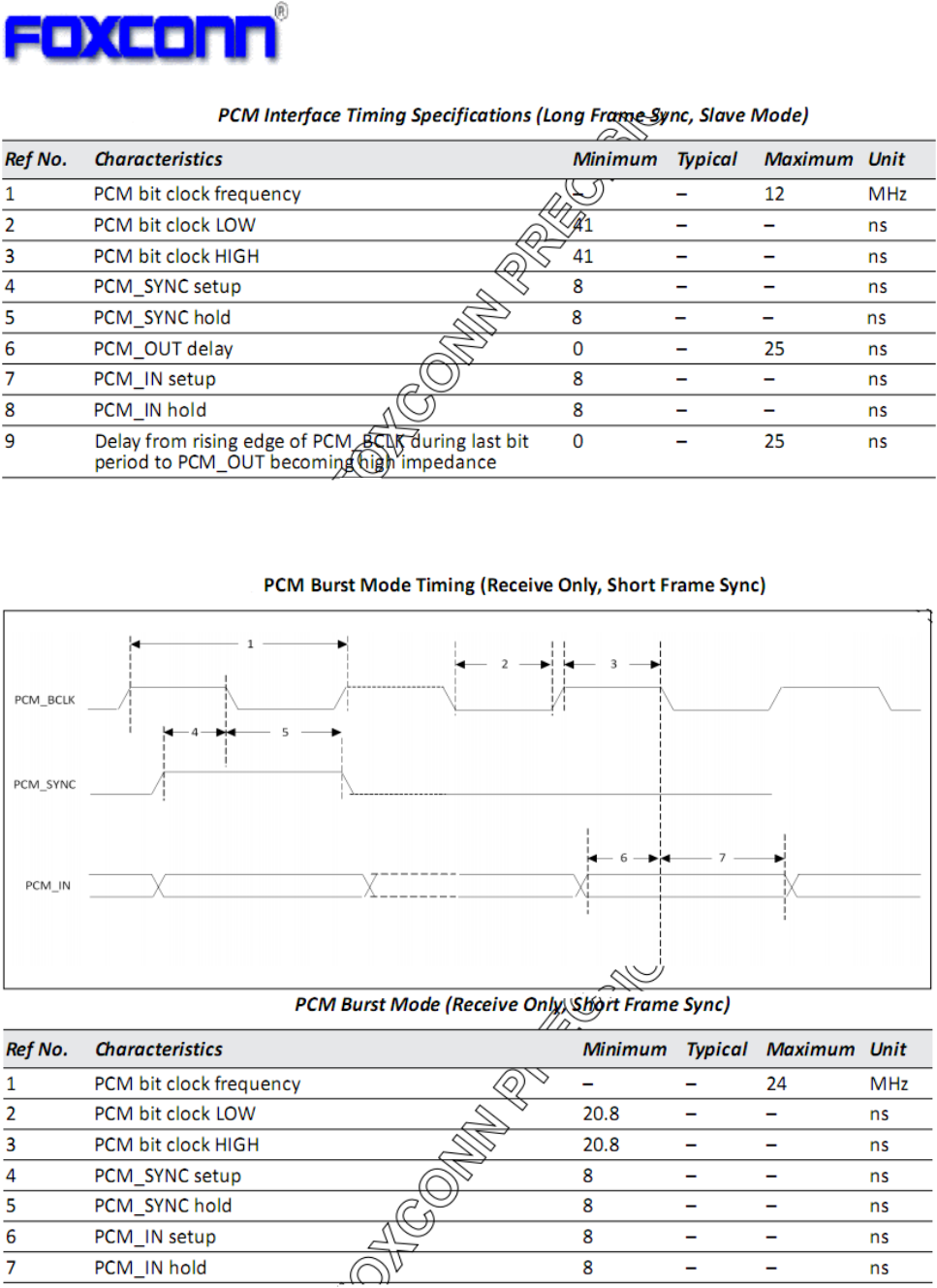
Receive Only, Short Frame Sync
COMPANY CONFIDENTIAL
Preliminary Datasheet
23
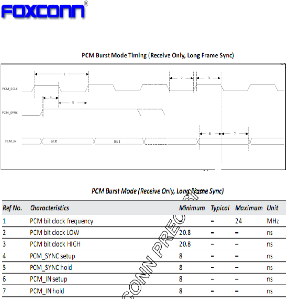
Receive Only, Long Frame Sync
COMPANY CONFIDENTIAL
Preliminary Datasheet
24
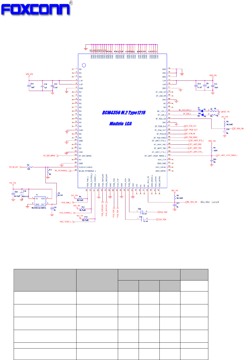
6.Schematic Reference Design
Following is the evaluation board schematics of M.2 1216 BCM4356 module for reference.
Low Power Clock
The BCM4356 module uses a secondary low frequency clock for low power mode timing. A precision
external 32.768 KHz clock that meets the specifications listed in Table 3 is required by BCM4356.
Table 3: External 32.768K Low Power Oscillator Specifications
Parameter
Conditions/
Notes
Specification
Units
Min
Typ
Max
Nominal
Input Frequency
32.768
-
KHz
Frequency Accuracy
-200
+200
ppm
Input signal amplitude
+0.2
+1.8
V, p-p
Duty cycle
Square waveor
sine- wave
30
-
70
%
Clock jitter
300Hz-15KHz
-
5
ns
Clock jitter
During initial
start-up
10,000
ppm
COMPANY CONFIDENTIAL
Preliminary Datasheet
25
Below section describes the directionality of some of the interface signals incorporated in
the various pinouts. Because some signals have directionality associated with them, their
names and locations may be different between the Platform side and the Module side.
The Module pinouts are described in Item2.5. The main differences between Platform-side
pinouts and Module-side pinouts are shown in Figure 95~96 of M.2 spec.
Figure 95: UART and PCM Signal Direction and Signal Name Changes

COMPANY CONFIDENTIAL
Preliminary Datasheet
26
7. Software Requirement(TBD)
- Operating System Support
Windows 8
Windows Blue or later Android 4.3 and above
- WLAN Feature Support
WiFi Direct
WiFi Display
Wi-Fi Miracast (Intel will support WiDi with Miracast interoperability)
- WLAN Security Support
WPA/WPA2 Enterprise
CCX Lite or higher
WMM/AES/TKIP/CKIP
- WLAN Transmit Power Reduction
Software control to meet FCC SAR requirement
Capability to disable 5GHz operation
- Bluetooth Profile Support
Advanced Audio Distribution Profile(A2DP)
Basic Imaging Profile (BIP)
Basic Printing Profile( BPP)
General Audio/Video Distribution Profile (GAVDP )
Generic Object Profile(GOEP)
Hands-Free Profile(HFP)
Headset Profile(HSP)
Human Interface Device Profile(HID)[2.0/4.0]
Object Push Profile (OPP)
Service Port Profile(SPP)
Personal Area Network Profile(PAN)
- BLE (Bluetooth Low Energy) Support
Windows 8
Windows Blue or later
8. Regulatory(TBD)
The module shall pass below RF certification based-on customer requirement.
USA : FCC P15B / FCC P15C / FCC P15E (FCC ID: TBD)
Canada : IC RSS-210 (IC ID: TBD)
Japan : TELEC
EU : EN300328 V1.8.1 , EN301893 V1.6.1 , EN301489-1/-17 , EN 60950-1 2nd
9. Quality
The product quality must be followed-up by Foxconn factory quality control system.
COMPANY CONFIDENTIAL
Preliminary Datasheet
27
10. Package information
Below is M.2 1216 package information for reference only.

COMPANY CONFIDENTIAL
Preliminary Datasheet
28
11. Environmental Requirements and Specifications
11.1 Temperature
11.1.1 Operating Temperature Conditions
The product shall be capable of continuous reliable operation when operating in ambient temperature of
0 °C to +70°C.
11.1.2 Non-Operating Temperature Conditions
Neither subassemblies shall be damaged nor shall the operational performance be degraded when
restored to the operating temperature when exposed to storage temperature in the range of -30°C to +85°C.
11.2 PCB bending
The PCB bending spec shall be keep planeness under 0.1mm for both Foxconn and end assembly
customer.
11.3 Handling environment
ESD
There are semiconductors on the module, please handle the module under ESD protected and
well-controlled environment (<100V).
Terminals Handling Notice
The product is mounted with motherboard through Land Grid Array. In order to prevent poor soldering,
please do not touch LGA portion by hand.
Notes: As a rule, baking the components in accordance with condition mentioned above, because tape and
real for packaging materials have no heat resistance, please bake the components moved into another
container such as heat resistance trays.
Others
1. Please make sure to avoid mechanical shock and vibration for this module.
2. Please do not drop the module.
3. Please do not clean the module.
11.4 Storage Condition
1. Moisture barrier bag must be stored under 40 ℃, humidity under 90% RH, when the moisture
barrier bag is sealed by Foxconn.
2. The calculated shelf life for the dry packed product shall be a 12 months from the bag seal date.
3. If Moisture barrier bag is open, the component must be stored in an environment of <25±5℃
/10%RH
4. Please keep the module at 30℃/70% RH.
11.5 Baking Condition
If below two conditions happens:
a) Humidity indicator cards read >30%
b) Temp < 30 ℃, Humidity <70%RH, moisture barrier bag open over 96 hours
Products require baking before mounting
Baking condition: 125 ℃, 12-22 hours
Baking times: Max. 2 times
COMPANY CONFIDENTIAL
Preliminary Datasheet
29
11.6 Soldering and reflow condition
1) Heating method
Conventional Convection or IR/convection
2) Temperature measurement
Thermocouple d=0.1mm ~ 0.2mm CA (K) or CC (T) at soldering portion or equivalent method.
3) Solder paste composition
Sn/3.0Ag/0.5Cu
4) Allowable reflow soldering times: 2 times, based on the below reflow soldering profile
Suggest reflow soldering one time for better reliability.
5) Temperature profile
Reflow soldering shall be done according to the below temperature profile.
6) Peak temp: 245 degree C
Temperature profile for evaluation of solder heat resistance of a
component (at solder joint)

1
Federal Communication Commission Interference Statement
This device complies with Part 15 of the FCC Rules. Operation is subject to the
following two conditions: (1) This device may not cause harmful interference, and
(2) this device must accept any interference received, including interference that
may cause undesired operation.
This equipment has been tested and found to comply with the limits for a Class B
digital device, pursuant to Part 15 of the FCC Rules. These limits are designed to
provide reasonable protection against harmful interference in a residential
installation. This equipment generates, uses and can radiate radio frequency energy
and, if not installed and used in accordance with the instructions, may cause
harmful interference to radio communications. However, there is no guarantee that
interference will not occur in a particular installation. If this equipment does cause
harmful interference to radio or television reception, which can be determined by
turning the equipment off and on, the user is encouraged to try to correct the
interference by one of the following measures:
- Reorient or relocate the receiving antenna.
- Increase the separation between the equipment and receiver.
- Connect the equipment into an outlet on a circuit different from that
to which the receiver is connected.
- Consult the dealer or an experienced radio/TV technician for help.
FCC Caution: Any changes or modifications not expressly approved by the party
responsible for compliance could void the user's authority to operate this equipment.
This transmitter must not be co-located or operating in conjunction with any other
antenna or transmitter.
Operations in the 5.15-5.25GHz band are restricted to indoor usage only.
Radiation Exposure Statement:
This equipment complies with FCC radiation exposure limits set forth for an
uncontrolled environment. This equipment should be installed and operated with
minimum distance 20cm between the radiator & your body.
This device is intended only for OEM integrators under the following conditions:
1) The antenna must be installed such that 20 cm is maintained between the
antenna and users, and
2) The transmitter module may not be co-located with any other transmitter or
antenna.
As long as 2 conditions above are met, further transmitter test will not be required.
However, the OEM integrator is still responsible for testing their end-product for any
additional compliance requirements required with this module installed
IMPORTANT NOTE: In the event that these conditions can not be met (for example
certain laptop configurations or co-location with another transmitter), then the FCC
authorization is no longer considered valid and the FCC ID can not be used on the
final product. In these circumstances, the OEM integrator will be responsible for

2
re-evaluating the end product (including the transmitter) and obtaining a separate
FCC authorization.
End Product Labeling
This transmitter module is authorized only for use in device where the antenna may
be installed such that 20 cm may be maintained between the antenna and users.
The final end product must be labeled in a visible area with the following: “Contains
FCC ID: MCLT77H566”. The grantee's FCC ID can be used only when all FCC
compliance requirements are met.
Manual Information To the End User
The OEM integrator has to be aware not to provide information to the end user
regarding how to install or remove this RF module in the user’s manual of the end
product which integrates this module.
The end user manual shall include all required regulatory information/warning as
show in this manual.
Industry Canada statement:
This device complies with RSS-210 of the Industry Canada Rules. Operation is subject to
the following two conditions: (1) This device may not cause harmful interference, and (2)
this device must accept any interference received, including interference that may cause
undesired operation.
Ce dispositif est conforme à la norme CNR-210 d'Industrie Canada applicable aux
appareils radio exempts de licence. Son fonctionnement est sujet aux deux conditions
suivantes: (1) le dispositif ne doit pas produire de brouillage préjudiciable, et (2) ce
dispositif doit accepter tout brouillage reçu, y compris un brouillage susceptible de
provoquer un fonctionnement indésirable.
Radiation Exposure Statement:
This equipment complies with IC radiation exposure limits set forth for an uncontrolled
environment. This equipment should be installed and operated with minimum distance
20cm between the radiator & your body.
Déclaration d'exposition aux radiations:
Cet équipement est conforme aux limites d'exposition aux rayonnements IC établies pour
un environnement non contrôlé. Cet équipement doit être installé et utilisé avec un
minimum de 20 cm de distance entre la source de rayonnement et votre corps.
This device is intended only for OEM integrators under the following conditions:
1) The antenna must be installed such that 20 cm is maintained between the antenna and
users, and
2) The transmitter module may not be co-located with any other transmitter or antenna.
As long as 2 conditions above are met, further transmitter test will not be required.
However, the OEM integrator is still responsible for testing their end-product for any
additional compliance requirements required with this module installed.

3
Cet appareil est conçu uniquement pour les intégrateurs OEM dans les conditions suivantes:
(Pour utilisation de dispositif module)
1) L'antenne doit être installée de telle sorte qu'une distance de 20 cm est respectée entre
l'antenne et les utilisateurs, et
2) Le module émetteur peut ne pas être coïmplanté avec un autre émetteur ou antenne.
Tant que les 2 conditions ci-dessus sont remplies, des essais supplémentaires sur
l'émetteur ne seront pas nécessaires. Toutefois, l'intégrateur OEM est toujours
responsable des essais sur son produit final pour toutes exigences de conformité
supplémentaires requis pour ce module installé.
IMPORTANT NOTE:
In the event that these conditions can not be met (for example certain laptop configurations
or co-location with another transmitter), then the Canada authorization is no longer
considered valid and the IC ID can not be used on the final product. In these
circumstances, the OEM integrator will be responsible for re-evaluating the end product
(including the transmitter) and obtaining a separate Canada authorization.
NOTE IMPORTANTE:
Dans le cas où ces conditions ne peuvent être satisfaites (par exemple pour certaines
configurations d'ordinateur portable ou de certaines co-localisation avec un autre
émetteur), l'autorisation du Canada n'est plus considéré comme valide et l'ID IC ne peut
pas être utilisé sur le produit final. Dans ces circonstances, l'intégrateur OEM sera chargé
de réévaluer le produit final (y compris l'émetteur) et l'obtention d'une autorisation distincte
au Canada.
End Product Labeling
This transmitter module is authorized only for use in device where the antenna may be
installed such that 20 cm may be maintained between the antenna and users. The final
end product must be labeled in a visible area with the following: “Contains IC:
2878D-T77H566”.
Plaque signalétique du produit final
Ce module émetteur est autorisé uniquement pour une utilisation dans un dispositif où
l'antenne peut être installée de telle sorte qu'une distance de 20cm peut être maintenue
entre l'antenne et les utilisateurs. Le produit final doit être étiqueté dans un endroit visible
avec l'inscription suivante: "Contient des IC: 2878D-T77H566".
Manual Information To the End User
The OEM integrator has to be aware not to provide information to the end user regarding
how to install or remove this RF module in the user’s manual of the end product which
integrates this module.
The end user manual shall include all required regulatory information/warning as show in
this manual.
Manuel d'information à l'utilisateur final
L'intégrateur OEM doit être conscient de ne pas fournir des informations à l'utilisateur final

4
quant à la façon d'installer ou de supprimer ce module RF dans le manuel de l'utilisateur
du produit final qui intègre ce module.
Le manuel de l'utilisateur final doit inclure toutes les informations réglementaires requises
et avertissements comme indiqué dans ce manuel.
Caution :
(i) the device for operation in the band 5150-5250 MHz is only for indoor use to reduce the
potential for harmful interference to co-channel mobile satellite systems;
(ii) the maximum antenna gain permitted for devices in the bands 5250-5350 MHz and
5470-5725 MHz shall comply with the e.i.r.p. limit; and
(iii) the maximum antenna gain permitted for devices in the band 5725-5825 MHz shall
comply with the e.i.r.p. limits specified for point-to-point and non point-to-point operation as
appropriate.
(iv) Users should also be advised that high-power radars are allocated as primary users
(i.e. priority users) of the bands 5250-5350 MHz and 5650-5850 MHz and that these radars
could cause interference and/or damage to LE-LAN devices.
Avertissement:
Le guide d’utilisation des dispositifs pour réseaux locaux doit inclure des instructions
précises sur les restrictions susmentionnées, notamment :
(i) les dispositifs fonctionnant dans la bande 5 150-5 250 MHz sont réservés uniquement
pour une utilisation à l’intérieur afin de réduire les risques de brouillage préjudiciable aux
systèmes de satellites mobiles utilisant les mêmes canaux;
(ii) le gain maximal d’antenne permis pour les dispositifs utilisant les bandes 5 250-5 350
MHz et 5 470-5 725 MHz doit se conformer à la limite de p.i.r.e.;
(iii) le gain maximal d’antenne permis (pour les dispositifs utilisant la bande 5 725-5 825
MHz) doit se conformer à la limite de p.i.r.e. spécifiée pour l’exploitation point à point et
non point à point, selon le cas.
(iv) De plus, les utilisateurs devraient aussi être avisés que les utilisateurs de radars de
haute puissance sont désignés utilisateurs principaux (c.-à-d., qu’ils ont la priorité) pour les
bandes 5 250-5 350 MHz et 5 650-5 850 MHz et que ces radars pourraient causer du
brouillage et/ou des dommages aux dispositifs LAN-EL.
Europe – EU Declaration of Conformity
This device complies with the essential requirements of the R&TTE Directive 1999/5/EC. The
following test methods have been applied in order to prove presumption of conformity
with the essential requirements of the R&TTE Directive 1999/5/EC:
- EN 60950-1/A12: 2011
Safety of Information Technology Equipment
- EN 62311: 2008 / Article 3(1)(a) and Article 2 2006/95/EC)
Assessment of electronic and electrical equipment related to human exposure
restrictions for electromagnetic fields (0 Hz-300 GHz) (IEC 62311:2007 (Modified))
5
- EN 300 328 V1.8.1: 2012
Electromagnetic compatibility and Radio spectrum Matters (ERM); Wideband
Transmission systems; Data transmission equipment operating in the 2,4 GHz ISM band
and using spread spectrum modulation techniques; Harmonized EN covering essential
requirements under article 3.2 of the R&TTE Directive
- EN 301 893 V1.7.1: 2012
Broadband Radio Access Networks (BRAN); 5 GHz high performance RLAN;
Harmonized EN covering essential requirements of article 3.2 of the R&TTE Directive
- EN 301 489-1 V1.9.2: 2011
Electromagnetic compatibility and Radio Spectrum Matters (ERM); ElectroMagnetic
Compatibility (EMC) standard for radio equipment and services; Part 1: Common
technical requirements
- EN 301 489-17 V2.2.1: 2012
Electromagnetic compatibility and Radio spectrum Matters (ERM); ElectroMagnetic
Compatibility (EMC) standard for radio equipment and services; Part 17: Specific
conditions for 2,4 GHz wideband transmission systems and 5 GHz high performance
RLAN equipment
Česky
[Czech]
[Jméno výrobce] tímto prohlašuje, že tento [typ zařízení] je ve shodě se základními požadavky a
dalšími příslušnými ustanoveními směrnice 1999/5/ES.
Dansk
[Danish]
Undertegnede [fabrikantens navn] erklærer herved, at følgende udstyr [udstyrets typebetegnelse]
overholder de væsentlige krav og øvrige relevante krav i direktiv 1999/5/EF.
Deutsch
[German]
Hiermit erklärt [Name des Herstellers], dass sich das Gerät [Gerätetyp] in Übereinstimmung mit den
grundlegenden Anforderungen und den übrigen einschlägigen Bestimmungen der Richtlinie
1999/5/EG befindet.
Eesti
[Estonian]
Käesolevaga kinnitab [tootja nimi = name of manufacturer] seadme [seadme tüüp = type of
equipment] vastavust direktiivi 1999/5/EÜ põhinõuetele ja nimetatud direktiivist tulenevatele teistele
asjakohastele sätetele.
English Hereby, [name of manufacturer], declares that this [type of equipment] is in compliance with the
essential requirements and other relevant provisions of Directive 1999/5/EC.
Español
[Spanish]
Por medio de la presente [nombre del fabricante] declara que el [clase de equipo] cumple con
los requisitos esenciales y cualesquiera otras disposiciones aplicables o exigibles de la Directiva
1999/5/CE.
Ελληνική
[Greek]
ΜΕ ΤΗΝ ΠΑΡΟΥΣΑ [name of manufacturer] ΔΗΛΩΝΕΙ ΟΤΙ [type of equipment] ΣΥΜΜΟΡΦΩΝΕΤΑΙ
ΠΡΟΣ ΤΙΣ ΟΥΣΙΩΔΕΙΣ ΑΠΑΙΤΗΣΕΙΣ ΚΑΙ ΤΙΣ ΛΟΙΠΕΣ ΣΧΕΤΙΚΕΣ ΔΙΑΤΑΞΕΙΣ ΤΗΣ ΟΔΗΓΙΑΣ 1999/5/ΕΚ.
Français
[French]
Par la présente [nom du fabricant] déclare que l'appareil [type d'appareil] est conforme aux
exigences essentielles et aux autres dispositions pertinentes de la directive 1999/5/CE.
Italiano
[Italian]
Con la presente [nome del costruttore] dichiara che questo [tipo di apparecchio] è conforme ai
requisiti essenziali ed alle altre disposizioni pertinenti stabilite dalla direttiva 1999/5/CE.
Latviski
[Latvian]
Ar šo [name of manufacturer / izgatavotāja nosaukums] deklarē, ka [type of equipment / iekārtas
tips] atbilst Direktīvas 1999/5/EK būtiskajām prasībām un citiem ar to saistītajiem noteikumiem.
Lietuvių
[Lithuanian]
Šiuo [manufacturer name] deklaruoja, kad šis [equipment type] atitinka esminius reikalavimus ir kitas
1999/5/EB Direktyvos nuostatas.
Nederlands
[Dutch]
Hierbij verklaart [naam van de fabrikant] dat het toestel [type van toestel] in overeenstemming is
met de essentiële eisen en de andere relevante bepalingen van richtlijn 1999/5/EG.
Malti Hawnhekk, [isem tal-manifattur], jiddikjara li dan [il-mudel tal-prodott] jikkonforma mal-ħtiġijiet
essenzjali u ma provvedimenti oħrajn relevanti li hemm fid-Dirrettiva 1999/5/EC.
6
[Maltese]
Magyar
[Hungarian]
Alulírott, [gyártó neve] nyilatkozom, hogy a [... típus] megfelel a vonatkozó alapvetõ
követelményeknek és az 1999/5/EC irányelv egyéb elõírásainak.
Polski
[Polish]
Niniejszym [nazwa producenta] oświadcza, że [nazwa wyrobu] jest zgodny z zasadniczymi
wymogami oraz pozostałymi stosownymi postanowieniami Dyrektywy 1999/5/EC.
Português
[Portuguese]
[Nome do fabricante] declara que este [tipo de equipamento] está conforme com os requisitos
essenciais e outras disposições da Directiva 1999/5/CE.
Slovensko
[Slovenian]
[Ime proizvajalca] izjavlja, da je ta [tip opreme] v skladu z bistvenimi zahtevami in ostalimi
relevantnimi določili direktive 1999/5/ES.
Slovensky
[Slovak]
[Meno výrobcu] týmto vyhlasuje, že [typ zariadenia] spĺňa základné požiadavky a všetky príslušné
ustanovenia Smernice 1999/5/ES.
Suomi
[Finnish]
[Valmistaja = manufacturer] vakuuttaa täten että [type of equipment = laitteen tyyppimerkintä]
tyyppinen laite on direktiivin 1999/5/EY oleellisten vaatimusten ja sitä koskevien direktiivin muiden
ehtojen mukainen.
Svenska
[Swedish]
Härmed intygar [företag] att denna [utrustningstyp] står I överensstämmelse med de väsentliga
egenskapskrav och övriga relevanta bestämmelser som framgår av direktiv 1999/5/EG.
低功率電波輻射性電機管理辦法
第十二條 經型式認證合格之低功率射頻電機,非經許可,公司、商號或使用者
均不得擅自變更頻率、加大功率或變更原設計之特性及功能。
第十四條 低功率射頻電機之使用不得影響飛航安全及干擾合法通信;經發現有
干擾現象時,應立即停用,並改善至無干擾時方得繼續使用。
前項合法通信,指依電信法規定作業之無線電通信。
低功率射頻電機須忍受合法通信或工業、科學及醫療用電波輻射性電機
設備之干擾。
在5.25-5.35秭赫頻帶內操作之無線資訊傳輸設備,限於室內使用。
1. 本模組於取得認證後將依規定於模組本體標示審驗合格標籤。
2. 系統廠商應於平台上標示「本產品內含射頻模組: XXXyyyLPDzzzz-x」字
樣。