HON HAI PRECISION IND T77W676 LTE Cat9 PCI Express M.2 Module User Manual Foxconn CNSBG
HON HAI Precision Ind. Co., Ltd. LTE Cat9 PCI Express M.2 Module Foxconn CNSBG
Users Manual rev.pdf
COMPANY CONFIDENTIAL
- 1 -
LTE-Advanced PCI Express M.2 Module
(LTE, UMTS)
Engineering Requirements Specification
Project code: T77W676.00
Solution: MDM9240+WTR3925+WTR4905
SKU: WW-3-S3
Copyright © 2017. Foxconn Communications Inc. All rights reserved.
COMPANY CONFIDENTIAL
- 2 -
Reviewers
Department Name Signature Review Dates
* Plan ** Results
Project Manager Choro.Chung
Project Leader Ai-ning Song
Hardware Engineer Yannie.Zhang
Modification History
Rev Date Originator Comment
D1.0 2016/12/13 Yannie.Zhang Initial release for customer discussion and carrier
engagement, will update it after hardware design frozen.
D1.1 2016/12/27 Yannie.Zhang Change the module picture and remark 1.8V MIPI.
D1.2 2017/2/24 Yannie.Zhang Update RF performance follow EVT design
D1.3 2017/05/10 Yannie.Zhang Upadte CA Combination.
D1.4 2017/08/02 Yannie.Zhang Update LTE B5 power’s spec.

COMPANY CONFIDENTIAL
- 3 -
CONTENTS
1.GENERAL DESCRIPTION ...................................................................... 5
1.1SYSTEM MAIN FEATURE ...................................................................... 6
1.2CARRIER AGGREGATION COMBINATION ...................................... 8
1.3SYSTEM BLOCK DIAGRAM ............................ 錯誤! 尚未定義書籤。
1.4PIN DEFINITION ....................................................................................... 9
1.5PLATFORM CONNECTION DESIGN ................................................. 11
2.HARDWARE FEATURES ..................................................................... 19
2.1 MOBILE DATA MODEM ............................................................................... 19
2.2 RF TRANSCEIVER ........................................................................................ 20
2.3 POWER MANAGEMENT IC ........................................................................ 21
2.4 ANTENNA DESIGN ....................................................................................... 22
3.MECHANICAL SPECIFICATIONS ...................................................... 25
3.1 OVERVIEW ..................................................................................................... 25
3.2 MECHANICAL CONSTRAINTS .................................................................. 25
3.3 M.2 CARD ASSEMBLY ................................................................................ 26
4.ELECTRICAL SPECIFICATIONS ........................................................ 29
4.1 RECOMMENDED OPERATING CONDITIONS ....................................... 29
4.2 POWER CONSUMPTION ............................................................................. 30
5.RF PERFORMANCE SPECIFICATIONS ........................................... 31
5.1 RF MAXIMUM TX POWER &RF MIN. RX SENSITIVITY
SPECIFICATIONS ................................................................................................ 31

COMPANY CONFIDENTIAL
- 4 -
6.HOST INTEGRATION INSTRUCTIONS ............................................. 33
COMPANY CONFIDENTIAL
5
1. General Description
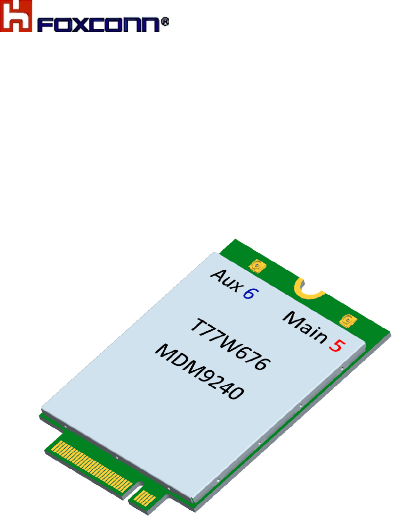
T77W676.00 is designed to enable wireless data connectivity for notebook computer or any
other device compatible with the PCI Express M.2 Specification 3042 type Key.B slot.
T77W676.00 is the data card solution that delivers wireless wide-area network (WWAN)
connectivity for the LTE, UMTS (HSDPA/HSUPA/HSPA+/DC-HSPA+) and
GPS/Glonass/Beidou protocols in one hardware configuration.
SKU WW-3-S3 / T77W676
Carrier Support
NA: AT&T, Verizon, Sprint
WW: Vodafone, Orange, Telefonica-O2
EU: Deutsche Telekom, Swisscom
APAC: Telstra, Optus, Docomo, KDDI
China: CMCC/CUCC/CTCC
* Carrier engagement based on real business agreement
QCT Solution MDM9240+WTR3925+WTR4905+PMD9645
4G
FDD FDD / TDD
Support Band B2/4/5/7/12/13/17/25/26/30/38/41/66
Carrier Aggregation 2CCs&3CCs DL CA, 2X2MIMO,
Up to inter-band 3CCs DL
Cat (DL/UL Mbps) Up to Cat11 @20MHz+20MHz+20MHz 3CCs DL CA
3G
WCDMA HSPA+ Rel8 (DL/UL: up to 42/11 Mbps)
Support Band Band4
GNSS GPS/GLONASS/Beidou
Interface USB2.0, USB3.0
Form factor 3042 PCIe M.2 Key.B

COMPANY CONFIDENTIAL
6
1.1 System Main Feature
Feature Description
Physical PCI express M.2 module, size 3042,Key.B,75Pin golden finger
Electrical Single VCC supply (3.135V~4.4V follow M.2 standard)
Dimension Dimensions (L × W × H): 42 mm × 30 mm × 2.3 mm,
maximum height=2.38mm (add PCB tolerance=0.08mm)
Shielding design Shield case on board design, no additional shielding
requirement
Weight Approximately ~6g
USIM Off-board USIM connector supported
Operating Bands
WCDMA/HSDPA/HSUPA/HSPA+ operating bands:
Band 4: 1710 to 1755 MHz (UL), 2110 to 2155 MHz (DL)
LTE FDD operating bands:
Band 2: 1850 to 1910 MHz (UL), 1930 to 1990 MHz (DL)
Band 4: 1710 to 1755 MHz (UL), 2110 to 2155 MHz (DL)
Band 5: 824 to 849 MHz (UL), 869 to 894 MHz (DL)
Band 7: 2500 to 2570 MHz (UL), 2620 to 2690 MHz (DL)
Band 12: 699 to 716 MHz (UL), 729 to 746 MHz (DL)
Band 13: 777 to 787 MHz (UL), 746 to 756 MHz (DL)
Band 17: 704 to 716 MHz (UL), 734 to 746 MHz (DL)
Band 25: 1850 to 1915 MHz (UL), 1930 to 1995 MHz (DL)
Band 26: 814 to 849 MHz (UL), 859 to 894 MHz (DL)
Band 30: 2305 to 2315 MHz (UL) 2350 to 2360 MHz (DL)
Band 38: 2570 to 2620 MHz (UL/DL)
Band 41: 2496 to 2690 MHz (UL/DL)
Band 66: 1710 to 1800 MHz (UL), 2110 to 2200 MHz (DL)
Diversity/2nd Rx All UMTS operating bands
All LTE operating bands
GNSS
GPS: L1 (1575.42MHz)
GLONASS: L1 (1602MHz)
Beidou (1561.098MHz)
USIM Voltage Support 1.8V and 2.85V, and auto detects follow SIM card type
Antenna connectors MAIN and AUX(supports Diversity and GPS simultaneously)
Throughput
WCDMA CS: DL 64 kbps /UL 64 kbps
WCDMA PS: DL 384 kbps /UL 384 kbps
HSPA+: DL 21.6 Mbps /UL 5.76 Mbps
DC-HSPA+: DL 42 Mbps/UL 5.76 Mbps
LTE Cat4: DL:150 Mbps/UL 50 Mbps
LTE Cat6: DL:300 Mbps/UL 50 Mbps
LTE Cat9: DL:450 Mbps/UL 50 Mbps
LTE Cat11: DL:585 Mbps/UL 50 Mbps

COMPANY CONFIDENTIAL
7
LTE air interface
LTE Rel11
z FDD: up to 585 Mbps downlink, 50 Mbps uplink
z Up to 20MHz+20MHz+20MHz Inter-band or Intra-band 3DL CA
z Support 256QAM in DL, 16QAM in UL (64QAM software upgradable)
z Support TDD+FDD CA (3GPP Rel12 feature)
z 1.4 to 20 MHz RF bandwidth
z Support downlink 4X2 MIMO
z IPv6, QoS
WCDMA/HSPA air interface
z R99:
All modes and data rates for WCDMA FDD
z R5 HSDPA
PS data speeds up to 7.2 Mbps on the downlink
z R6 HSUPA
E-DCH data rates of up to 5.76 Mbps for 2 ms TTI (UE category 6) uplink
z R7 HSPA+
Downlink 64 QAM SISO: up to 21 Mbps
Downlink 16 QAM 2X2 MIMO: up to 28 Mbps
Uplink 16 QAM: up to 5.76 Mbps
z R8 DC-HSPA+
Downlink dual carrier with 64 QAM (SISO); up to 42 Mbps
z IPv6
GNSS
z Customizable tracking session
• Automatic tracking session on startup
• Concurrent standalone GPS, GLONASS and BeiDou
• gpsOneXTRA with GPS + GLONASS + BeiDou support

COMPANY CONFIDENTIAL
8
1.2 Carrier aggregation combination
1.2.1. Refer to Qualcomm documents 80-NR113-650, Rev.E, Published: 03-16-2016.
Remark: T77W676 hardware design can support follow CA combination, but the Final CA
combinations plan depends on carrier engagement and Qualcomm software design.
1.2.2. Qualcomm MDM9240 support 3CA+256QAM(up to Cat11) and partial Rel12
(FDD+TDD CA) which is mandatory for AU/JP/China carriers.
Region Carriers 2CCs DL CA Combinations 3CCs DL CA Combinations
NA AT&T,
VZW,
Sprint,
TMO,
Canada
B2 + B2, B2 + B4, B2 + B5,
B2 + B12, B2 + B13, B2 +
B17, B2 + B29, B2 + B30, B4
+ B4, B4 + B5, B4 + B7, B4
+ B12, B4 + B13, B4 + B17,
B4 + B29, B4 + B30, B5 +
B30, B12 + B12, B12 + B30,
B25 + B25, B25 + B26, B25
+ B41, B26 + B41, B29 +
B30, B41 + B41,
B2+B66, B5+B66, B12+B66,
B13+B66, B66+B66,
B29+B66
B2 + B2 + B12, B2 + B2 + B13,B2 +
B4 + B5, B2 + B4 + B12, B2 + B4 +
B13, B2 + B4 + B29, B2 + B5 + B30,
B2 + B12 + B12, B2 + B12 + B30, B2
+ B29 + B30, B4 + B4 + B5, B4 + B4
+ B12, B4 +B4 +B13, B4 + B5 + B30,
B4 + B12 + B12, B4 + B12 + B30, B4
+ B29 + B30, B25 + B26 + B41, B25
+ B41 + B41, B26 + B41 + B41, B41
+ B41 + B41
B13+B66+B2, B12+B66+B66,
B13+B66+B66, B5+B66+B2,
B5+B66+B66, B66+B66+B2,
B66+B66+B66
Korea SKT,KT,
LGU+
B1 + B5, B3 + B5, B3 + B8,
B5 + B7
B1 + B3 + B5, B1 + B3 + B8, B1 +
B5 + B7, B1 + B7 + B28, B3 + B7 +
B8
JP KDDI,
DCM,
SBM
B1 + B3, B1 + B8, B1 + B18,
B1 + B19, B1 + B26, B3 +
B19, B19 + B21, B41 + B41
B1 + B3 + B19, B1 + B3 + B28, B1 +
B41 + B41, B41 + B41 + B41
EU Various B1 + B20, B3 + B3, B3 + B7,
B3 + B20, B3 + B38, B7 +
B7, B7 + B8, B7 + B20, B38
+ B38
B1 + B3 + B20, B1 + B7 + B20, B3 +
B3 + B7, B3 + B3 + B20, B3 + B7 +
B20, B3 + B7 + B7, B3 + B20 + B38,
B3 + B38 + B38
China CMCC,
CTCC,
CUCC
B1 + B3, B1 + B26, B3 +
B26, B3 + B40, B39 + B39,
B39 + B41, B40 + B40, B41
+ B41
B1 + B3 + B3, B1 + B3 + B26, B1 +
B3 + B41, B3 + B40 + B40, B39 +
B39 + B41, B39 + B41 + B41, B40 +
B40 + B40, B41 + B41 + B41
AU/SE
A/LA
Tel st r a
/Optus
B1 + B3, B1 + B7, B1 + B28,
B3 + B8, B3 + B28, B5 + B7,
B5 + B40, B7 + B8, B7 +
B28
B3 + B3 + B8, B3 + B7 + B7, B3 +
B7 + B28, B7 + B7 + B28, B3 + B40
+ B40, B28 + B40 + B40, B40 + B40
+ B40
COMPANY CONFIDENTIAL
9
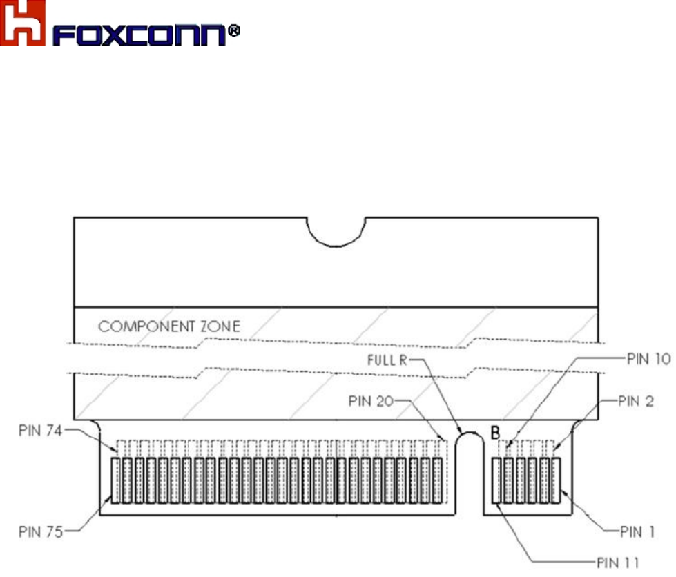
1.3 Pin definition
1.3.1 Golden finger Pin sequence
Figure 1-2 shows the sequence of pins on the 75-pin signal interface of M.2 3042 Key.B.
COMPANY CONFIDENTIAL
10
1.4.2 Pin definition
Table 1-1 M.2 Pin definition.
CONFIG_2 (GND) 75
74 3.3V GND 73
72 3.3V GND 71
70 3.3V CONFIG_1 (GND) 69
68 SUSCLK(32kHz) (I)(0/3.3V) Not connect in
T77W676
RESET# (I)(0/1.8V) 67
66 SIM DETECT (I) ANTCTL3 (O)(0/1.8V) 65
64 COEX_TXD (O)(0/1.8V) Dual layout
3GPIOs and
UART I/F for
LTE / Wi-Fi
coexistence
ANTCTL2 (O)(0/1.8V) 63
62 COEX_RXD(I)(0/1.8V) ANTCTL1 (O)(0/1.8V) 61
60 COEX3(I/O)(0/1.8V) ANTCTL0 (O)(0/1.8V) 59
58 MIPI_DATA (0/1.8V) For external
tunable
antenna (MiPi)
GND 57
56 MIPI_CLK (0/1.8V) REFCLKP 55 Reserved, but SW
disable in default
54 PEWAKE# (IO)(0/3.3V) Reserved, but
SW disable in
default
REFCLKN 53 Reserved, but SW
disable in default
52 CLKREQ# (IO)(0/3.3V) Reserved, but
SW disable in
default
GND 51
50 PERST# (I)(0/3.3V) Reserved, but
SW disable in
default
PERp0 49 Reserved, but SW
disable in default
48 GPIO_4 TX_BLANKING (0/1.8V*) PERn0 47 Reserved, but SW
disable in default
46 GPIO_3 SYSCLK (0/1.8V*) Not connect in
Foxconn
design
GND 45
44 GPIO_2 GNSS_IRQ (0/1.8V*) Reserved PETp0 43 Reserved, but SW
disable in default
42 GPIO_1 GNSS_SDA(0/1.8V*) Reserved PETn0 41 Reserved, but SW
disable in default
40 GPIO_0 GNSS_SCL (0/1.8V*) Reserved GND 39
38 Not connect USB3.0Rx+ 37
36 UIMPWR (O) USB3.0Rx 35
34 UIMDATA (IO) GND 33
32 UIMCLK (O) USB3.0Tx+ 31
30 UIMRESET (O) USB3.0Tx 29
28 GPIO_8 AUDIO_3 (IO) (0/1.8V) GND 27
26 GPIO_10 W_DISABLE2# (I) (0/3.3.V) 3.3V I/O DPR (I)(0/3.3V) 25 3.3V I/O
24 GPIO_7 AUDIO_2 (IO) (0/1.8V) GPIO_11 WoWWA
N# (O)(0/1.8V)
23
22 GPIO_6 AUDIO_1 (IO)(0/1.8V) CONFIG_0 (GND) 21
20 GPIO_5 AUDIO_0 (IO)(0/1.8V) Module Key 13~19
12~18 Module Key GND 11
10 GPIO_9 LED#1 (O)(Open drain) USB_D 9
8 W_DISABLE1# (I)(0/3.3V) 3.3V I/O USB_D+ 7
6 FULL_CARD_POWER_OFF# (I)(0/3.3V) 3.3V I/O GND 5
4 3.3V GND 3
2 3.3V CONFIG_3 (N/C) 1
Notes: Foxconn will provide one excel file to explain the PCIe M.2 Pin connection after
project award.
COMPANY CONFIDENTIAL
11
1.4 Platform connection design
1.5.1 Configuration Pins
The M.2 module provides 4 configuration pins. T77W676 is configured as WWAN-USB3.0 0,
refer to PCIe M.2_Rev 1.1.
Item Module configuration decodes Module type Port configuration
Config Config_0 Config_1 Config_2 Config_3
WWAN-USB3.0 0 Pin No. 21 69 75 1
State GND GND GND NC
1.5.2 Power and ground
(1) Power Rail Parameters
Parameter Min Type Max Units
Operating voltage 3.135 3.3 4.4 Vdc
The operating voltage was defined in PCIe M.2_Rev 1.1 standard as 3.135V~4.4V.
(2) 3.135 V is the minimum voltage supplied to LTE M.2 card by the host platform, and VCC
must never be under 3.135 V in any case. As our experiment, if we set the VCC=3.0V, the
M.2 card will power off possibly when M.2 card working at +23dBm continue mode.
(3) The LTE M.2 module provides 5 power pins and 11 Ground pins. To ensure that the LTE
module works normally, all the pins must be connected.
COMPANY CONFIDENTIAL
12
1.5.3 Full_Card_Power_Off
The M.2 LTE module can be controlled to power on/off by the Full_Card_Power_Of pin.
Item State M.2 card state
1 Low Powers off, It’s internally pulled down by 100K ohm resistor
2 High Powers on, it is 3.3V tolerant but can be driven by either 1.8V or
3.3V GPIO.
The recommended connections as below
1.5.4 USB3.0 interface
T77W676 module is compliant with USB3.0 in all modes. When two devices are connected
via a USB3.0 interface, one of the devices must act as a host, and the other device must act
as a peripheral. The host is responsible for initiating and controlling traffic on the bus.
Figure 1-3 USB3.0 interface.
COMPANY CONFIDENTIAL
13
1.5.5 W_DISABLE#
This control setting is implementation-specific and represents the collective intention of the
host software to manage radio operation. T77W676 provides a hardware pin (W_DISABLE#)
to disable or enable the radio. Besides, the radio can also be enabled or disabled through
software AT commands.
Item State Function (WWAN state)
W_DISABLE#1 Low WWAN Disabled (no RF operation allowed)
High WWAN Enabled (RF operation allowed), internally pull up
W_DISABLE#2 Low GPS Disabled (no RF operation allowed)
High GPS Enabled (RF operation allowed), internally pull up
Note: W_Disable# is connected to configurable GPIO pin from PMIC, which can support
either 3.3V VIO or 1.8V VIO. The default configuration is 3.3V VIO with interrupt function
(low active), 1.8V will not disable RF function.
1.5.6 LED Indication
The LED signal is provided to enable wireless communication add-in cards to provide status
indications to users via system provided indicators
(1) State of the LED# pin
Item State Definition Interpretation
1 Low The LED is emitting light. Radio is capable of transmitting.
2 High The LED is emitting no light. Radio is incapable of transmitting.
(2) Typical LED Connection in Platform/System
.
COMPANY CONFIDENTIAL
14
1.5.7 WoWWAN
The WAKE_ON_WWAN# signal is for power saving.
•LTE module always listening at very low power in idle mode
•LTE module will wake up mother board via ‘WoWWAN’ signal.
•The platform will power on when triggered by the LTE module.
The WAKE_ON_WWAN# signal is used to wake up the host. It is open drain and should be
pulled up at the host side. When the WWAN needs to wake up the host, it will output a one
second low pulse, shown in Figure 1-4.
Typical Connection in Platform/System
COMPANY CONFIDENTIAL
15
1.5.8 DPR (Dynamic Power Reduction)
The optional DPR signal is used by wireless devices to assist in meeting regulatory SAR
(Specific Absorption Rate) requirements for RF exposure. The signal is provided by a host
system proximity sensor to the wireless device to provide an input trigger causing a
reduction in the radio transmit output power.
The required value of the power reduction will vary between different host systems and is
left to the host platform OEM and card vendor to determine, along with the specific
implementation details. The assertion and de-assertion of DPR is asynchronous to any
system clock. All transients resulting from the proximity sensor need to be de-bounced by
system circuitry.
(1) State of the DPR
Item State Definition Interpretation
1 Low
Enable the SAR power back off. Radio is capable of transmitting.
2 High
Disable the SAR power back off,
internally pull up Radio is incapable of transmitting.
Note: DPR is connected to configurable GPIO pin from PMIC, which can support either 3.3V
VIO or 1.8V VIO. The default configuration is 3.3V VIO with interrupt function (low active),
1.8V will not enable DPR function.
(2) Typical Connection in Platform/System
Remark:
a. The proximity sensor was controlled by the platform side.
b. After DPR pin becomes low level, you can set the MAX TX power by AT commands..
COMPANY CONFIDENTIAL
16
1.5.9 USIM
The UIM contains parameters necessary for the WWAN device’s operation in a wireless
wide area network radio environment. The UIM signals are described in the following
paragraphs for M.2 add-in cards that support the off-card UIM interface.
(1) USIM card socket
It is recommended to take electrostatic discharge (ESD) protection measures near the USIM
card socket. The USIM socket should be placed near the NGFF interface (<100 mm),
because a long circuit may impact signal quality.
(2) UIM-PWR
UIM_PWR power supply can supply 1.8 V and 2.85 V power to UIM card and auto detects
follow SIM card type
(3) SIM Detect
This signal is used to detect the insertion and removal of a SIM device in the SIM socket.
With a Normal Short SIM Card connector, PUSH-PUSH type, the detect switch is normally
shorted to ground when no SIM card is inserted. When the SIM is inserted, the
SIM_DETECT will transition from logic 0 to logic 1 state. The rising edge will indicate
insertion of the SIM card. When the SIM is pulled out, the SIM_DETECT will transition from
logic1 to logic 0. This falling edge will indicates the pulling out of the SIM card. The M.2
module monitoring this signal will treat the rising/falling edge or the actual logic state as an
interrupt, that when triggered, the module will act accordingly.
The UIM_PWR from the PRODUCT shall be turned ON 2 seconds after UIM_DETECT pin
is asserted to HIGH. This is to ensure the power is not turned ON earlier before SIM card to
be seated well.
COMPANY CONFIDENTIAL
17
1.5.10 Antenna Control
(1).T77W676 provides GPIO control signals for external antenna tuner application.
ANTCTRL (0-3) are provided to allow for the implementation of antenna tuning solutions.
The number antenna control lines required will depend on the application and antenna/band
requirements. We will provide a tool to fill antenna control table in ODM factory to enable
antenna tuner support on specific platforms.
Foxconn general design for WWAN module with two control signals for reference only.
ANTCTL0 ANTCTL1 Frequency (MHz) Band support
0 0 880 ~ 960 Band8 (WCDMA) + GSM900 + High Bands
0 1 791 ~ 894 Band5 (WCDMA, LTE) + GSM850 + High Bands
1 0 746 ~787 Band13 (LTE) + High Bands
1 1 704 ~746 Band17 (LTE) + High Bands
(2). T77W676 also provides MIPI interface (VIO=1.8V) for external antenna tuner
application.The function is under development for customization. M.2 pin.56 (MIPI_CLK), 58
(MIPI_DATA) are provided to allow for the implementation of antenna tuner solutions with
variable capacitors. We will provide a tool to fill MIPI registers in ODM factory to enable
antenna tuner support on specific platforms.
1.5.11 Coexistence
COEX1, COEX2 and COEX3 are provided to allow for the implementation of wireless
coexistence solutions between the radio(s) on the M.2 Card and other off-card radio(s).
These other radios can be located on another M.2 Card located in the same host platform or
as alternate radio implementations (for example, using a PCI Express M.2 CEM or a
proprietary form-factor add-in solution).
We also dual layout UART Tx/Rx with COEX1 and COEX2 for future extension, please
contact with us if need to use these Pins.
Item Signal name Description
COEX1 LTE_ACTIVE (COEX_TXD) TBD
COEX2 LTE_FRAME_SYNC (COEX_RXD) TBD
COEX3 LTE_WLAN_PRIORITY TBD
COMPANY CONFIDENTIAL
18
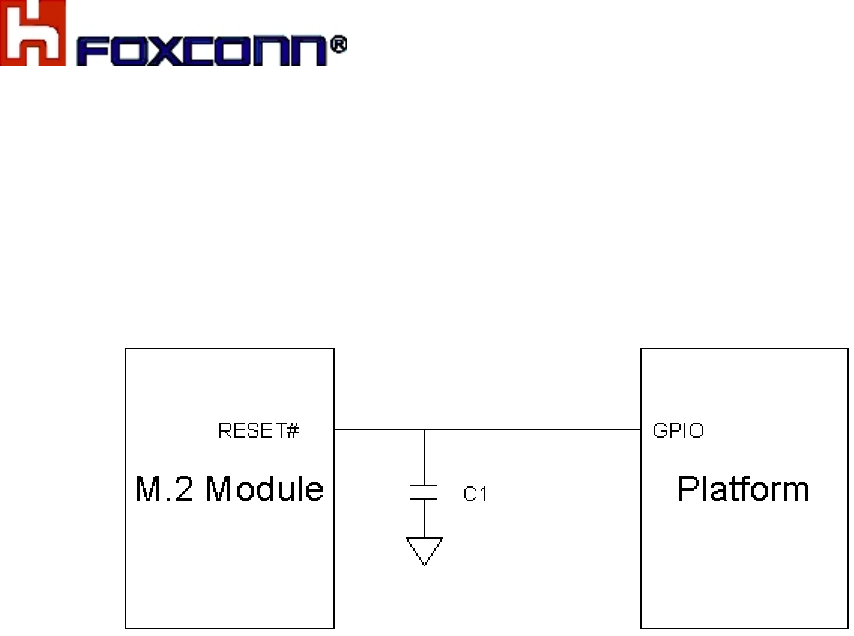
1.5.12 RESET#
Asynchronous RESET# pin, active low. Whenever this pin is active, the modem will
immediately be placed in a Power On reset condition. Care should be taken not to activate
this pin unless there is a critical failure and all other methods of regaining control and/or
communication with the WWAN sub-system have failed.
The Reset# signal is relatively sensitive, it is recommended to install one capacitor
(10~100pF) near to the M.2 card pin.

COMPANY CONFIDENTIAL
19
2. Hardware features
T77W676.00 consists of the following key engine components, in addition to the required
front-end RF and other discrete components.
Modem engine
■ Soft Baseband: MDM-9240
■ RF: WTR3925 and WTR4905
■ Power: PMD9645
Connectivity engine
■ USB: USB3.0
■ USIM: located off board
■ Antenna: connectors for the off board antennas
2.1 Mobile Data Modem
The MDM9x40 chipset supports high-speed data capabilities over a wide range of air
interface standards; the supported RF operating bands are defined by the chipset’s
RFICs. They are complete system solutions that operate on networks worldwide. The major
functions of MDM9240 used on T77W676.00 are listed below:
❒ Processor:
- Manufactured in 20nm CMOS process
- System uP (Cortex-A7 up to 1.19 GHz with 256 kB L2 cache)
❒ Memory:
- External memory
EBI1: 2Gb LPDDR2, 32-bit LPDDR2 SDRAM at up to 518 MHz
- External memory
EBI2: 2Gb NAND flash
❒ Air interface:
- WCDMA (R99, HSDPA, HSUPA, HSPA+, DC-HSPA+)
- LTE (R11 Cat6/9/11, FDD/TDD)
- GPS/Glonass/Beidou
❒ Advance RX operation:
- Mobile receive diversity (WCDMA, LTE)
❒ Connectivity:
- USB 3.0 with built-in USB PHY

COMPANY CONFIDENTIAL
20
- UART interface
- UIM support (dual voltage)
2.2 RF transceiver
In order to support 3DL CA, there are two RF transceivers in T77W676, include WTR3925
and WTR4905. WTR3925 is designed for high bands and middle bands, and WTR4905 is
for low bands and GNSS. Both of them are the RF transceiver ICs within compatible
Qualcomm MDM9240 chipsets.
2.2.1.1 Key features of WTR3925
z Qualcomm Technologies, Inc. (QTI) fourth-generation
z 4G/3G/2G transceiver
z First 28 nm CMOS, wafer-level package
z First single-chip LTE-carrier aggregation (CA)
z First RF transceiver to support 40 MHz CA
z Support for intraband and interband CA
z Significant increase in number of RF ports
z Dedicated feedback receiver
z Integrated GPS core – GPS/Glonass/BeiDou
2.2.1.2 Key benefits of WTR3925
z Enables a single PCB design for global platforms
z Significant power consumption and size reduction over previous generations
z > 25% current consumption savings
z > 50% direct package area savings
z LTE-A, HSPA+, UMTS, CDMA, TD-S, and GSM
z Spectrum support: 700‒2700 MHz
z Supporting all newly specified and planned spectrums
z Support for 28 Rx ports and 10 Tx ports
z Reduces external components – lowers cost
z Single-ended inputs, easier PCB routing
2.2.2.1 Key features of WTR4905
z QTI fifth-generation LTE transceiver
z LTE, HSPA+, UMTS, CDMA, TD-S, and GSM
z First RF transceiver to support SAWless 2G
z Second 28 nm CMOS, wafer-level package

COMPANY CONFIDENTIAL
21
z Supports B28 APAC 700 MHz
z Significant increase in the number of Rx ports
z Dedicated feedback receiver
z Integrated GPS core
z GPS/GLONASS/BeiDou with no eLNA
2.2.2.2 Key benefits of WTR4905
z Smaller size (10 mm2) with more functionality
z Spectrum support: 700–2700 MHz
z Supports all newly specified spectrums (including B28)
z Support for eight Rx ports and five Tx ports
z Enables a single PCB design for emerging markets
z Reduces number of external switches
z No Rx SAW required for 2G bands
z Significant current consumption savings over previous generations
z > 30% for 3G talk and > 50% for 4G Cat-3
z Significant size reduction over previous generations
2.3 Power management IC
T77W676.00 system uses the Qualcomm PMD9645. The PMD9645 device integrates all
the wireless product’s power management, general housekeeping, and user interface
support functions into a single mixed-signal IC. Its versatile design is suitable for any
multimode, multiband product.Since the PMD9645 includes so many diverse functions, its
operation is more easily understood by considering major functional blocks individually.
Therefore, the PMD9645 document set is organized by the following device functionality:
z Input power management
z Output power management
z General housekeeping
z User interfaces
z IC interfaces
z Configurable pins—either multipurpose pins (MPPs) or general-purpose
inputs/outputs (GPIOs)—that can be configured to function within some of the other
categories
COMPANY CONFIDENTIAL
22
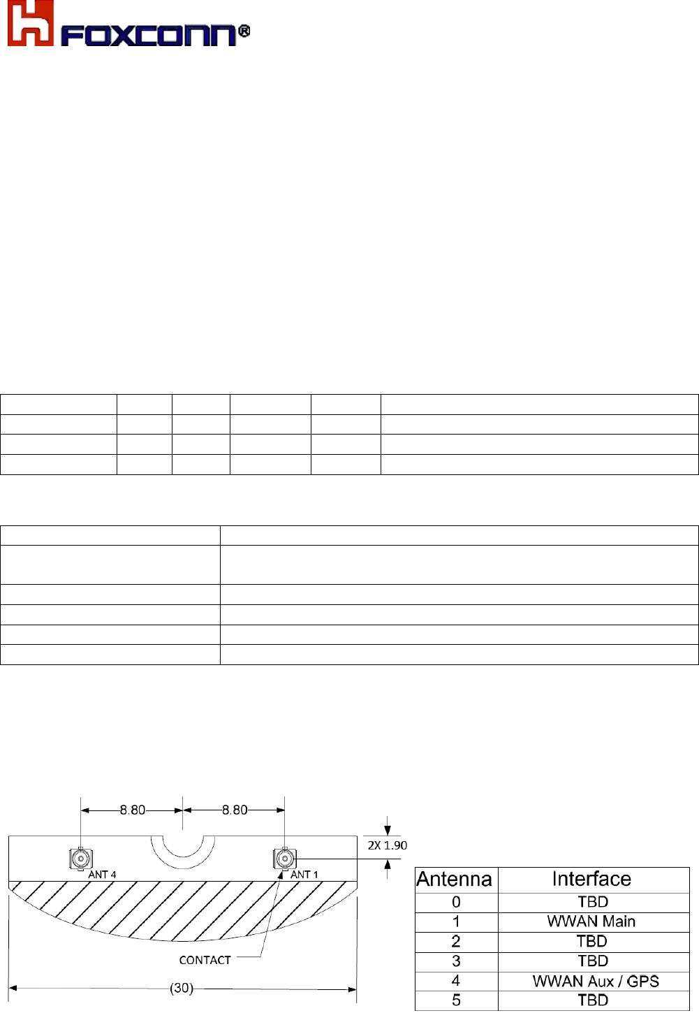
2.4 Antenna Design
2.4.1 Antenna specification
T77W676.00 also provides connectivity for off board antennas. The antennas and their
connection interface for this device satisfy the requirements specified in the PCI Express
M.2 Specification Revision Version 1.0 standard. The antenna elements are typically
integrated into the notebook/ultrabook /tablet and connected to T77W676.00 module via
flexible RF coaxial cables. T77W676.00 provides two RF connectors (MHF type), one for
the primary transmitter/receiver port and the other for the diversity receiver and GNSS.
To ensure stable RF performance, customer must assemble adequate antenna according to
the antenna specification.
Table 2-1 Main antenna specifications
Parameter Min. Typ. Max. Units Notes
Cable loss / / 0.5 dB Maximum loss to antenna
Impedance / 50 / Ohm Antenna load impedance
VSWR / / 3:1 / Maximum allowed VSWR of antenna
Table 2-2 Aux antenna specifications
Parameter
Gain Maximum gain and uniform converge in high angle elevation
and zenith. Gain in the azimuth is not desired.
Average 3D gain >-5dBi
VSWR Typical value <3:1
Isolation(diversity to Main) >10dB in all related bands
Polarization Any
2.4.2 Antenna location and mechanical design.
To ensure customer has a clear knowledge of the two antennas, check below product
picture.
Figure 2-1 Antenna connector location and type
COMPANY CONFIDENTIAL
23
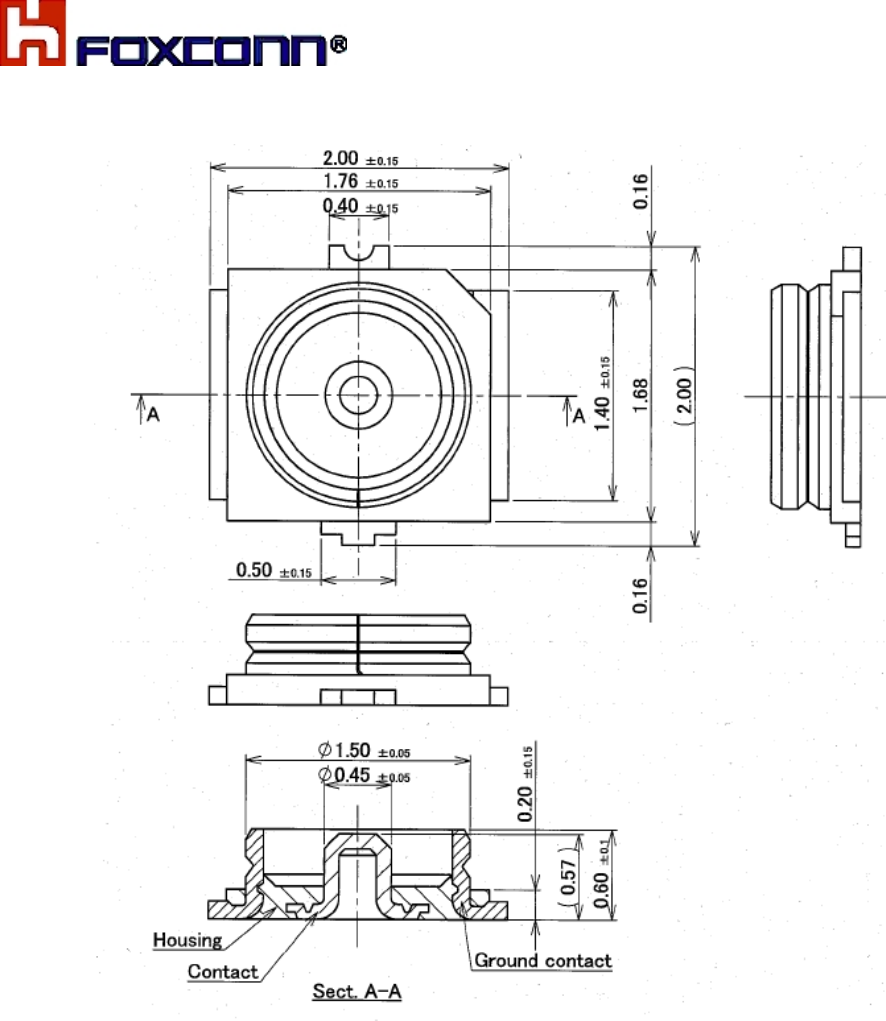
Figure 2-2 RF connectors
COMPANY CONFIDENTIAL
24
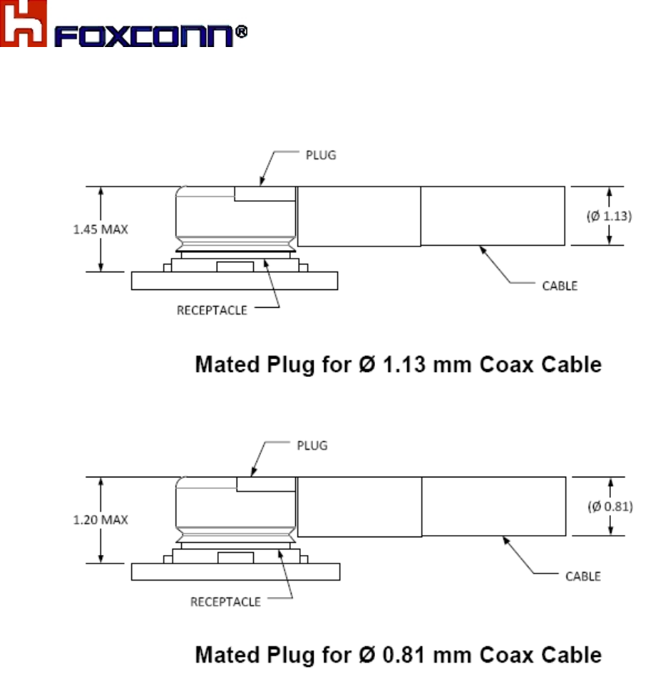
Figure 2-3 RF receptacles
COMPANY CONFIDENTIAL
25
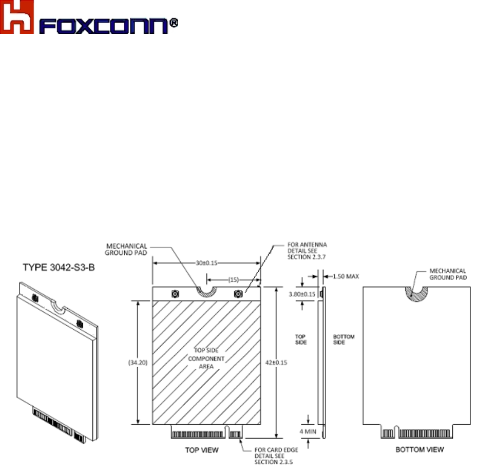
3. Mechanical Specifications
3.1 Overview
T77W676.00 is compatible with the PCI Express M.2 Specification 3042 Key.B type 75-pin
card edge-type connector. Refer to Electromechanical Specification Revision 0.7a, Version
1.0 with Input Power and Voltage Tolerance ECN for more details.
3.2 Mechanical constraints
Figure 3-1 shows the mechanical constraints of T77W676.00 (3042-S3-B)
COMPANY CONFIDENTIAL
26
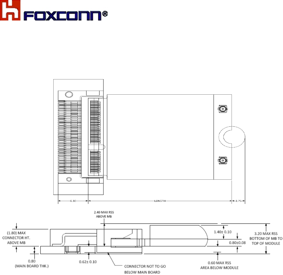
3.3 M.2 card assembly
Figure 3-2 shows Stack-up Mid-Line (In-line) Single Sided Module for 1.5 Maximum
Component Height, refer to section 2.4.8.3.1 of PCIe M.2_Rev 1.1 standard.
Remark:
a. 2.4mm maximum above mother board
b. Cut area of main board under M.2 module
c. Need to add thermal pad between M.2 module and mechanical component (like material
shielding) for thermal dissipation.
COMPANY CONFIDENTIAL
27
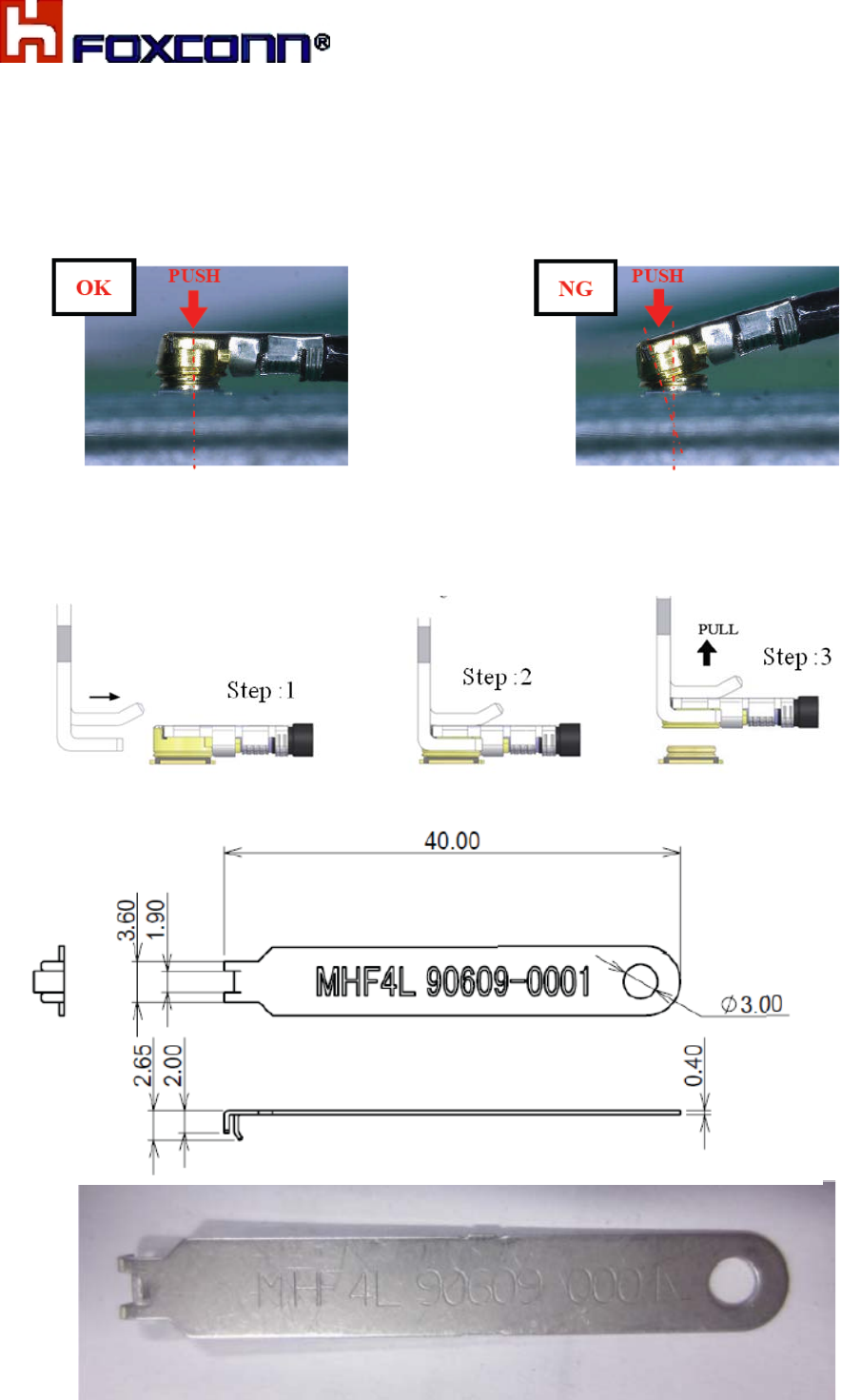
3.4 Connector assembly
a. Mate the connector vertically as much as possible. Adjusting the mating axis of plug
and receptacle. Do not slant mate.
.
b. Unmating: In case of unmating by pulling tool. Use the pulling tool as the following
drawing, and pull plug to vertical direction as directly as possible
c. Pulling tool(Unit:mm)

COMPANY CONFIDENTIAL
28
4. Electrical Specifications
4.1 Recommended operating conditions
Table 4-1 Recommended operating conditions
Parameter Min Type Max Units
Storage temperature -30 +25 +85 °C
Recommend operating temperature
(3GPP compliant)
-10 +25 +55 °C
Restricted operating temperature(*1)
(operational, non-3GPP compliant)
-20 +25 +70 °C
Extendable (with limited performance)
Temperature measure on T77W676 module(*2)
-40 +85
Operating voltage 3.135 3.3 4.4 Vdc
(1).Restricted operation allows normal mode data transmission for limited time until
automatic thermal shutdown takes effect. Within the restricted temperature range (outside
the operating temperature range) the specified electrical characteristics may be in or
decreased.
(2).Due to temperature measurement uncertainly, a tolerance on the stated shutdown
thresholds may occur. The possible deviation is in the range of +/- 2 ℃ at the
over-temperature and under-temperature limit.
Operating T77W676.00 device under conditions beyond its absolute maximum ratings
(Table 4-1) may damage the device. Absolute maximum ratings are limiting values to be
considered individually when all other parameters are within their specified operating ranges.
Functional operation and specification compliance under any absolute maximum condition,
or after exposure to any of these conditions, is not guaranteed or implied. Exposure may
affect device reliability

COMPANY CONFIDENTIAL
29
4.2 Power consumption
Table 4-2 Radio system power consumption
Test condition
Estimated power
range goal
(Typical)
Estimated power
range goal
(Max.)
WCDMA in suspend mode <5mA
WCDMA (Tx=24dBm) <800mA <1500mA
LTE in suspend mode <5mA
LTE (16QAM) Tx=23 dBm <900mA <1200mA
LTE CA mode, Tx=23dBm <1100mA <2200mA
GPS/GNSS tracking <150mA <300mA
Connected standby <3mA
Radio Off <3mA

COMPANY CONFIDENTIAL
30
5. RF performance specifications
Radio performance for T77W676.00 is given in the following sections, including RF receiver,
RF transmitter.
5.1 RF maximum Tx power &RF min. Rx sensitivity specifications
Table 5-1 Conducted Maximum transmit power & Min. receiver sensitivity (LTE BW: 10MHz)
Notes: The below test result is for reference only, we will update the Rx sensitivity after EVT
build before Feb. of 2017.
Band
3GPP
Standard
(dBm)
MFG
Spec.
(dBm)
PRx
(dBm)
DRx
(dBm)
MIMO
Combined
(dBm)
3GPP,MIMO
Combined (dBm)
1 23 +/-2 23 +/-1 -97.5 -97 -100 -95
2 23 +/-2 23 +/-1 -98 -97 -100 -95
3 23 +/-2 23 +/-1 -98.5 -97 -100 -94
4 23 +/-2 23 +/-1 -97 -97 -100 -97
5 23 +/-2 23 +2/-1 -99 -100 -102 -95
7 23 +/-2 23 +/-1 -98.5 -97 -100 -95
8 23 +/-2 23 +/-1 -99.5 -99.5 -102.5 -94
12 23 +/-2 23 +/-1 -99 -99 -102 -94
13 23 +/-2 23 +/-1 -99 -98.5 -101.5 -94
17 23 +/-2 23 +/-1 -99 -99 -102 -94
18 23 +/-2 23 +/-1 -99 -99 -102 -97
19 23 +/-2 23 +/-1 -99 -99 -102 -97
20 23 +/-2 23 +/-1 -99 -98.5 -101.5 -94
21 23 +/-2 23 +/-1 -98 -98 -101 -97
25 23 +/-2 23 +/-1 -98 -97 -100 -93.5
26 23 +/-2 23 +/-1 -99 -99 -102 -94.5
28 23 +/-2 23 +/-1 -98.5 -99 -101 -95.5
29 23 +/-2 23 +/-1 -98 -98 -101 -94
30 23 +/-2 23 +/-1 -97 -96.5 -100 -97
38 23 +/-2 23 +/-1 -97.5 -97 -100 -97
39 23 +/-2 23 +/-1 -98 -98 -100 -97
40 23 +/-2 23 +/-1 -97 -97 -100 -97
41 23 +/-2 23 +/-1 -97.5 -96 -99 -96
66 23 +/-2 23 +/-1 -97 -97 -100 -96.5
WCDMA
3GPP
Standard
(dBm)
MFG
Spec.
(dBm)
PRx
(dBm)
DRx
(dBm)
MIMO
Combined
(dBm)
3GPP,MIMO
Combined (dBm)
1 24+1.7/-3.7 23.5+/-1 -109 -109 -112 -106.7dBm
2 24+1.7/-3.7 23.5+/-1 -109 -109 -112 -104.7dBm
4 24+1.7/-3.7 23.5+/-1 -109 -109 -112 -106.7dBm
5(6/19) 24+1.7/-3.7 23.5+/-1 -110 -110 -113 -104.7dBm
8 24+1.7/-3.7 23.5+/-1 -110 -110 -113 -103.7dBm
COMPANY CONFIDENTIAL
31
GNSS
tracking
sensitivity
Design
target
(dBm)
Spec
(dBm)
-159 -152
Remark:
a. It has 3dB margin at least refer to 3GPP standard.
b. The typical value of LTE was measured as combine Rx sensitivity which was follow test
setup of 3GPP standard (TS36.521 charter 7.2 and charter 7.3.5), the test setup is follow
TS36.508 Annex A Figure A.3.
c. Above table is for general application, please inform us if you have any specific
requirement.
SS
RX/TX
RX
UE under Test
RX/TX
Ior
Îo
r
Splitter/
combiner

COMPANY CONFIDENTIAL
32
6. Host integration instructions
Install module through golden finger.
FederalCommunicationCommissionInterferenceStatement
ThisdevicecomplieswithPart15oftheFCCRules.Operationissubjecttothefollowingtwoconditions:(1)
Thisdevicemaynotcauseharmfulinterference,and(2)thisdevicemustacceptanyinterferencereceived,
includinginterferencethatmaycauseundesiredoperation.
ThisequipmenthasbeentestedandfoundtocomplywiththelimitsforaClassBdigitaldevice,pursuantto
Part15oftheFCCRules.Theselimitsaredesignedtoprovidereasonableprotectionagainstharmful
interferenceinaresidentialinstallation.Thisequipmentgenerates,usesandcanradiateradiofrequency
energyand,ifnotinstalledandusedinaccordancewiththeinstructions,maycauseharmfulinterferenceto
radiocommunications.However,thereisnoguaranteethatinterferencewillnotoccurinaparticular
installation.Ifthisequipmentdoescauseharmfulinterferencetoradioortelevisionreception,whichcan
bedeterminedbyturningtheequipmentoffandon,theuserisencouragedtotrytocorrecttheinterference
byoneofthefollowingmeasures:
‐ Reorientorrelocatethereceivingantenna.
‐ Increasetheseparationbetweentheequipmentandreceiver.
‐ Connecttheequipmentintoanoutletonacircuitdifferentfromthat
towhichthereceiverisconnected.
‐ Consultthedealeroranexperiencedradio/TVtechnicianforhelp.
FCCCaution:Anychangesormodificationsnotexpresslyapprovedbythepartyresponsibleforcompliance
couldvoidtheuser'sauthoritytooperatethisequipment.
Thistransmittermustnotbeco‐locatedoroperatinginconjunctionwithanyotherantennaortransmitter.

COMPANY CONFIDENTIAL
33
Radiation Exposure Statement:
This equipment complies with FCC radiation exposure limits set forth for an uncontrolled
environment. This equipment should be installed and operated with minimum distance 20cm
between the radiator & your body.
This device is intended only for OEM integrators under the following conditions:
ThisdeviceisintendedonlyforOEMintegratorsunderthefollowingconditions:
Theantennamustbeinstalledsuchthat20cmismaintainedbetweentheantennaandusers,and
Thetransmittermodulemaynotbeco‐locatedwithanyothertransmitterorantenna.
Aslongas2conditionsabovearemet,furthertransmittertestwillnotberequired.However,theOEM
integratorisstillresponsiblefortestingtheirend‐productforanyadditionalcompliancerequirements
requiredwiththismoduleinstalled
IMPORTANTNOTE:Intheeventthattheseconditionscannotbemet(forexamplecertainlaptop
configurationsorco‐locationwithanothertransmitter),thentheFCCauthorizationisnolongerconsidered
validandtheFCCIDcannotbeusedonthefinalproduct.Inthesecircumstances,theOEMintegratorwillbe
responsibleforre‐evaluatingtheendproduct(includingthetransmitter)andobtainingaseparateFCC
authorization.
EndProductLabeling
Thistransmittermoduleisauthorizedonlyforuseindevicewheretheantennamaybeinstalledsuchthat20
cmmaybemaintainedbetweentheantennaandusers.Thefinalendproductmustbelabeledinavisible
areawiththefollowing:“ContainsFCCID:MCLT77W676”.Thegrantee'sFCCIDcanbeusedonlywhenallFCC
compliancerequirementsaremet.
ManualInformationTotheEndUser
TheOEMintegratorhastobeawarenottoprovideinformationtotheenduserregardinghowtoinstallor
removethisRFmoduleintheuser’smanualoftheendproductwhichintegratesthismodule.
Theendusermanualshallincludeallrequiredregulatoryinformation/warningasshowinthismanual.
Industry Canada statement:
This device complies with ISED’s licence-exempt RSSs. Operation is subject to the following
two conditions: (1) This device may not cause harmful interference, and (2) this device must
accept any interference received, including interference that may cause undesired operation.
Le présent appareil est conforme aux CNR d’ ISED applicables aux appareils radio exempts
de licence. L’exploitation est autorisée aux deux conditions suivantes : (1) le dispositif ne doit
pas produire de brouillage préjudiciable, et (2) ce dispositif doit accepter tout brouillage reçu, y
compris un brouillage susceptible de provoquer un fonctionnement indésirable.
Radiation Exposure Statement:
The product comply with the Canada portable RF exposure limit set forth for an uncontrolled
environment and are safe for intended operation as described in this manual. The further RF
exposure reduction can be achieved if the product can be kept as far as possible from the user
body or set the device to lower output power if such function is available.
Déclaration d'exposition aux radiations:
Le produit est conforme aux limites d'exposition pour les appareils portables RF pour les
Etats-Unis et le Canada établies pour un environnement non contrôlé.
Le produit est sûr pour un fonctionnement tel que décrit dans ce manuel. La réduction aux
expositions RF peut être augmentée si l'appareil peut être conservé aussi loin que possible du
corps de l'utilisateur ou que le dispositif est réglé sur la puissance de sortie la plus faible si une
telle fonction est disponible.
This device is intended only for OEM integrators under the following conditions: (For
module device use)
1) The transmitter module may not be co-located with any other transmitter or antenna.
As long as 1 condition above are met, further transmitter test will not be required. However, the
OEM integrator is still responsible for testing their end-product for any additional compliance
requirements required with this module installed.
34
Cet appareil est conçu uniquement pour les intégrateurs OEM dans les conditions
suivantes: (Pour utilisation de dispositif module)
1) Le module émetteur peut ne pas être coïmplanté avec un autre émetteur ou antenne.
Tant que les 1 condition ci-dessus sont remplies, des essais supplémentaires sur l'émetteur ne
seront pas nécessaires. Toutefois, l'intégrateur OEM est toujours responsable des essais sur
son produit final pour toutes exigences de conformité supplémentaires requis pour ce module
installé.
IMPORTANT NOTE:
In the event that these conditions can not be met (for example certain laptop configurations or
co-location with another transmitter), then the Canada authorization is no longer considered
valid and the IC ID can not be used on the final product. In these circumstances, the OEM
integrator will be responsible for re-evaluating the end product (including the transmitter) and
obtaining a separate Canada authorization.
NOTE IMPORTANTE:
Dans le cas où ces conditions ne peuvent être satisfaites (par exemple pour certaines
configurations d'ordinateur portable ou de certaines co-localisation avec un autre émetteur),
l'autorisation du Canada n'est plus considéré comme valide et l'ID IC ne peut pas être utilisé
sur le produit final. Dans ces circonstances, l'intégrateur OEM sera chargé de réévaluer le
produit final (y compris l'émetteur) et l'obtention d'une autorisation distincte au Canada.
35

End Product Labeling
The product can be kept as far as possible from the user body or set the device to lower output
power if such function is available. The final end product must be labeled in a visible area with
the following: “Contains IC: 2878D-T77W676”.
Plaque signalétique du produit final
L'appareil peut être conservé aussi loin que possible du corps de l'utilisateur ou que le
dispositif est réglé sur la puissance de sortie la plus faible si une telle fonction est disponible.
Le produit final doit être étiqueté dans un endroit visible avec l'inscription suivante: "Contient
des IC: 2878D-T77W676".
Manual Information To the End User
The OEM integrator has to be aware not to provide information to the end user regarding how
to install or remove this RF module in the user’s manual of the end product which integrates
this module.
The end user manual shall include all required regulatory information/warning as show in this
manual.
Manuel d'information à l'utilisateur final
L'intégrateur OEM doit être conscient de ne pas fournir des informations à l'utilisateur final
quant à la façon d'installer ou de supprimer ce module RF dans le manuel de l'utilisateur du
produit final qui intègre ce module.
Le manuel de l'utilisateur final doit inclure toutes les informations réglementaires requises et
avertissements comme indiqué dans ce manuel.
低功率電波輻射性電機管理辦法
本模組於取得認證後將依規定於模組本體標示審驗合格標籤。
2. 系統廠商應於平台上標示「本產品內含射頻模組: XXXyyyLPDzzzz-x」字樣。
電磁波警語標示:「減少電磁波影響,請妥適使用」。
標示方式:必須標示於設備本體適當位置及設備外包裝及使用說明書上。
「電
36