HON HAI PRECISION IND T77H747 NFC Module User Manual rev 4
HON HAI Precision Ind. Co., Ltd. NFC Module rev 4
UserManual.wiki
>
HON HAI PRECISION IND
>
T77H747 User Manual
>
User Manual rev 4
Contents
1.
User Manual rev 4
2.
User Manual rev 4.pdf
3.
Users Manual rev2
4.
User Manual
User Manual rev 4
Navigation menu
Upload a User Manual
Namespaces
Wiki Guide
HTML
PDF
Info
Views
User Manual
Discussion / Help
Navigation
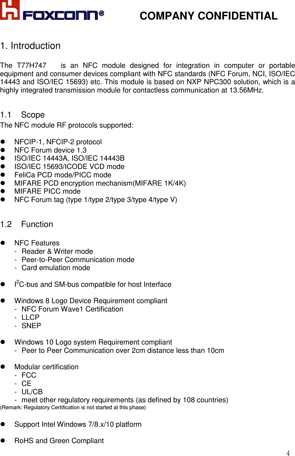
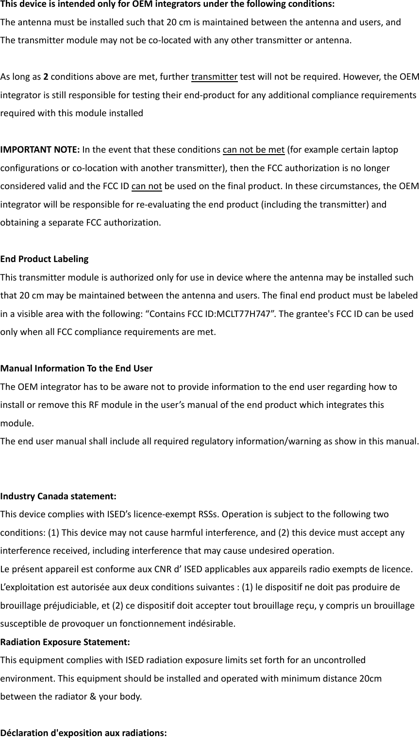
![COMPANY CONFIDENTIAL 16 2> Pin characteristics VEN input pin characteristics Symbol Parameter Conditions Min Typ Max Unit VIH HIGH-level input voltage 1.1 - VBAT V VIL LOW-level input voltage 0 - 0.4 V IIH HIGH-level input current VEN voltage=VBAT - - 1 µA IIL LOW-level input current VEN voltage=0V 1 - - µA Ci Input capacitance - 5 - pF Pin characteristics for IRQ, and TX_PWR_REQ Symbol Parameter Conditions Min Typ Max Unit VOH HIGH-level output voltage IOH<3mA - - - - IRQ and CLK_REQ pin VPVDD -0.4 - VPVDD V TX_PWR_REQ pin VDD-0.4 - VDD V VOL LOW-level output voltage IOL<3mA 0 - 0.4 V CL Load capacitance - - 20 pF tf Fall time CL=12pF max High speed 1 - 3.5 ns Low speed 2 - 10 ns tr Rise time CL=12pF max High speed 1 - 3.5 ns Low speed 2 - 10 ns Rpd Pull-down resistance IRQ and CLK_REQ pins [1] 0.35 - 0.85 MΩ TX_PWR_REQ pin [1] 55 - 120 kΩ [1] Activated in HPO and Monitor states. Input pin characteristics for DWL_REQ Symbol Parameter Conditions Min Typ Max Unit VIH HIGH-level input voltage VPVDD=1.8V 0.65*VPVDD - - V VIL LOW-level input voltage V PVDD=1.8V - - 0.35*VPVDD V VIH HIGH-level input voltage VPVDD=3V 2 - - V VIL LOW-level input voltage VPVDD=3V - - 0.8 V IIH HIGH-level input current - - 1 µA IIL LOW-level input curent 1 - - µA Ci Input capacitance - 5 - pF Rpd Pull down resistance Extra pull-down 0.35 - 0.85 MΩ Pin characteristics for HIF3(used as I2C-bus SDA) and HIF4(used as I2C-bus SCL) Symbol Parameter Conditions Min Typ Max Unit VOL LOW-level output voltage IOL<3mA [1] 0 - 0.4 V CL Load capacitance - - 10 pF tf Fall time CL=100 pF; [1] Rpull-up=2kΩ; Standard and Fast mode 30 - 250 ns CL=100 pF; [1] Rpull-up=1kΩ; High-speed mode 80 - 110 ns tr Rise time CL=100 pF; [1] Rpull-up=2kΩ; Standard and Fast mode 30 - 250 ns CL=100 pF; [1] Rpull-up=1kΩ; High-speed mode 10 - 100 ns VIH HIGH-level input voltage 0.7 *VPVDD - VPVDD V VIL LOW-level input voltage 0 - 0.3*VPVDD V IIH HIGH-level input current VI= VPVDD; high impedance - - 1 µA IIL LOW-level input current VI=0V; high impedance -1 - - µA Ci Input capacitance - 5 - pF [1] Only for pin HIF3(I2C-bus SDA), HIF4(I2C-bus SCL) is only used as input.](https://usermanual.wiki/HON-HAI-PRECISION-IND/T77H747.User-Manual-rev-4/User-Guide-3127142-Page-16.png)
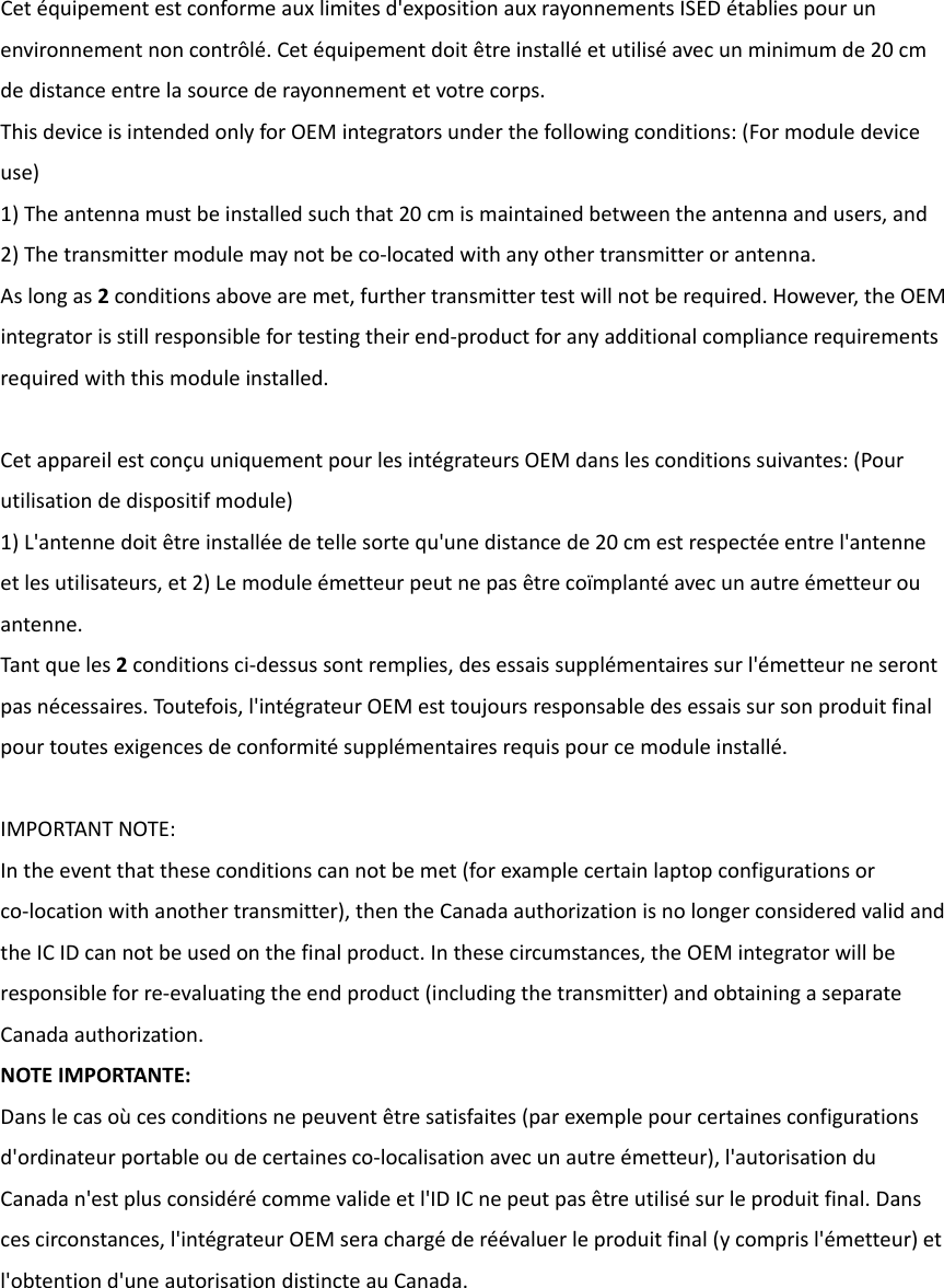
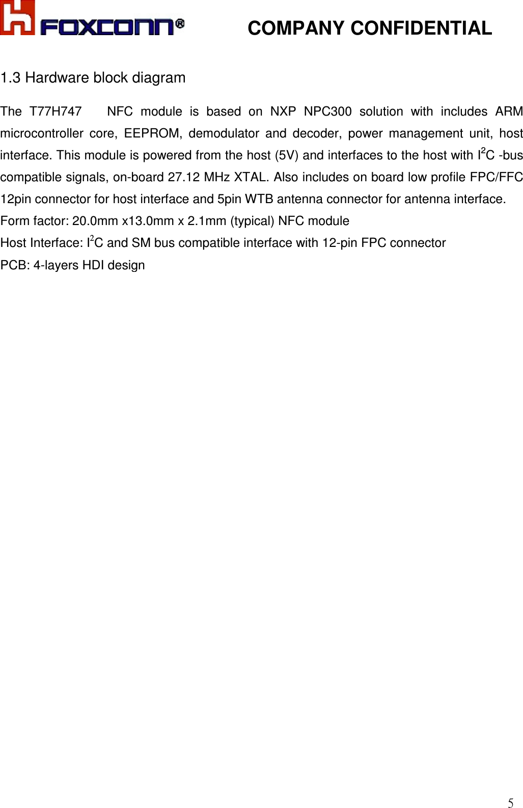
![COMPANY CONFIDENTIAL 17 SWIO_UICC pin characteristics Symbol Parameter Conditions Min Typ Max Unit VOH HIGH-level output voltage IIH=1mA; [1] IDD(SIM)=50mA; VDD(SIM_PMU)=2.75V; VDD(SIM_PMU) in class B 1.4 - - V VOH HIGH-level output voltage ISIM_SWIO=1mA; [1] IDD(SIM)=30mA; VDD(SIM_PMU)=1.67V; VDD(SIM_PMU) in class C 0.85 VDD(SIM) - - V VOH HIGH-level output voltage IIH =1mA; [1] IDD(SIM)=5mA; VDD(SIM_PMU)=0V; VDD(SIM)-VDDD 0.85 VDD(SIM) - - V VOL LOW-level output voltage 0µA<IIL<20Μa [1] - - 0.15VDD(SIM) V IIH HIGH-level input current - 300 - µA [1] To allow for overshoot, the voltage on SWIO shall remain between -0.3V and VOHmax+0.3V during dynamic operation. 3> Recommend FPC cable .](https://usermanual.wiki/HON-HAI-PRECISION-IND/T77H747.User-Manual-rev-4/User-Guide-3127142-Page-17.png)