HON HAI PRECISION IND T77H747 NFC Module User Manual rev 4
HON HAI Precision Ind. Co., Ltd. NFC Module rev 4
Contents
- 1. User Manual rev 4
- 2. User Manual rev 4.pdf
- 3. Users Manual rev2
- 4. User Manual
User Manual rev 4.pdf
COMPANY
CONFIDENTIAL
1
NFC
(Near Field Communication)
NXP NPC300 Module
Project Name
NFC (NXP NPC300) Module
Document Rev.
5.0
FOXCONN Part No.
T77H747.10
Module Rev.
005
FRU Part No.
01AX745
Customer Part No.
SW10K97523
FOXCONN Label Rev
00S0
Prepared by
Reviewed by
Approved by
Bandy.Jiang
Wei.Liao
Chang-Fu Lin
Revision
Note
COMPANY
CONFIDENTIAL
2
Revision History
Revision
Date
Originator
Comment
1.0
2016/01/28
Smile. Ming
Initial release
2.0
2016/04/20
Bandy.Jiang
1> Add pin 1 marking for mechanical drawing.
2> Add SM bus support in addition to I2C bus. (in
page 4,5)
3> Add description of pin9 (TX_PWR_REQ) signal
with active high 1.8V level output. (in page 15)
4> Change the PN of antenna connector from
BM05B-ACHSS-A-GAN-ETF(LF)(SN) to BM05B-
ACHKS-A-GAN-ETF(HF)
5> Update material in shielding drawing.
6> Following the latest schematic, update the
material description into BOM
7> Add Tray ID label, Carton label, Pallet label into
label information
8> Update packing information
3.0
2016/04/26
Bandy.Jiang
1> Update Module picture in page 18
2> Update packing information in page 23~24
3> Update vendor PN of host interface connector in
page 15
4.0
2016/06/24
Bandy.Jiang
1> Remove R5 from BOM.
2> Change Foxconn project name from T77H747.00
to T77H747.10
3> Change FRU part No. from 00JT548 to
01AX745.
4> Based on above change list, update module
picture, BOM, label contents and packing
information.
5.0
2016/06/28
Bandy. Jiang
1> Change Host JST part number from ACHR-05V-
A-S to ACHR-05V-A-K(HF) in page 14
T77H747.10 is made in China,
Manufactured by HongFuJin Precision Industry Co., LTD
Manufacture Site: ChongQing
http://www.foxconn.com

COMPANY
CONFIDENTIAL
3
Content
1.
INTRODUCTION ........................................................................................................................................................... 4
1.1
SCOPE ....................................................................................................................................................................... 4
1.2
FUNCTION.................................................................................................................................................................. 4
1.3
HARDWARE BLOCK DIAGRAM ....................................................................................................................................... 5
2.
ELECTRICAL CHARACTERISTICS ........................................................................................................................... 6
2.1
OPERATING CONDITIONS .............................................................................................................................................. 6
2.1
HOST INTERFACE CHARACTERISTICS .......................................................................................................................... 7
2.2
POWER-UP SEQUENCE ................................................................................................................................................ 8
2.3
POWER-DOWN SEQUENCE ........................................................................................................................................... 9
2.4
FUNCTION TIMING CHARACTERISTICS ......................................................................................................................... 9
3.
NFC CONTACTLESS STANDARD CONFORMANCE .......................................................................................... 10
3.1
FREQUENCY INTEROPERABILITY ................................................................................................................................ 10
3.2
SUPPORTED SMART CARD TYPES .............................................................................................................................. 10
3.3
CONTACTLESS INTERFACE UNIT ................................................................................................................................ 11
4.
MECHANICAL ARCHITECTURE .............................................................................................................................. 12
4.1
MODULE MECHANICAL DRAWING .............................................................................................................................. 12
4.2
ANTENNA INTERFACE OF NFC MODULE .................................................................................................................... 13
4.3.
HOST INTERFACE OF NFC MODULE ......................................................................................................................... 15
4.4.
SHIELDING COVER OF NFC MODULE ....................................................................................................................... 18
4.5.
PICTURE OF NFC MODULE ....................................................................................................................................... 18
5.
PCB PATTERN OF NFC MODULE .......................................................................................................................... 19
5.1
PCB COMPONENT PLACEMENT ................................................................................................................................. 19
5.2
PCB STACK UP AND MATERIALS .............................................................................................................................. 19
6.
BOM (BILL OF MATERIALS) OF NFC MODULE ................................................................................................... 20
7.
MARKING INFORMATION ........................................................................................................................................ 21
8.
PACKING INFORMATION ......................................................................................................................................... 23

COMPANY
CONFIDENTIAL
4
1.
Introduction
The T77H747.10 is an NFC module designed for integration in computer or portable
equipment and consumer devices compliant with NFC standards (NFC Forum, NCI, ISO/IEC
14443 and ISO/IEC 15693) etc. This module is based on NXP NPC300 solution, which is a
highly integrated transmission module for contactless communication at 13.56MHz.
1.1 Scope
The NFC module RF protocols supported:
•
NFCIP-1, NFCIP-2 protocol
•
NFC Forum device 1.3
•
ISO/IEC 14443A, ISO/IEC 14443B
•
ISO/IEC 15693/ICODE VCD mode
•
FeliCa PCD mode/PICC mode
•
MIFARE PCD encryption mechanism(MIFARE 1K/4K)
•
MIFARE PICC mode
•
NFC Forum tag (type 1/type 2/type 3/type 4/type V)
1.2 Function
•
NFC Features
-
Reader & Writer mode
-
Peer-to-Peer Communication mode
-
Card emulation mode
•
I2C-bus and SM-bus compatible for host Interface
•
Windows 8 Logo Device Requirement compliant
-
NFC Forum Wave1 Certification
-
LLCP
-
SNEP
•
Windows 10 Logo system Requirement compliant
-
Peer to Peer Communication over 2cm distance less than 10cm
•
Modular certification
-
FCC
-
CE
-
UL/CB
-
meet other regulatory requirements (as defined by 108 countries)
(Remark: Regulatory Certification is not started at this phase)
•
Support Intel Windows 7/8.x/10 platform
•
RoHS and Green Compliant
COMPANY
CONFIDENTIAL
5
1.3 Hardware block diagram
The T77H747.10 NFC module is based on NXP NPC300 solution with includes ARM
microcontroller core, EEPROM, demodulator and decoder, power management unit, host
interface. This module is powered from the host (5V) and interfaces to the host with I2C -bus
compatible signals, on-board 27.12 MHz XTAL. Also includes on board low profile FPC/FFC
12pin connector for host interface and 5pin WTB antenna connector for antenna interface.
Form factor: 20.0mm x13.0mm x 2.1mm (typical) NFC module
2
Host Interface: I C and SM bus compatible interface with 12-pin FPC connector
PCB: 4-layers HDI design
The functional block diagram is shown as below:
COMPANY
CONFIDENTIAL
6
2.
Electrical Characteristics
2.1 operating conditions
Absolute Maximum Rating
Symbol
Condition
Min.
Typ.
Max
Unit
VBAT
Respect to GND
--
5.0
6.0
V
PVDD
Respect to GND
--
3.3
4.35
V
ESD Limit Level
HBM
--
--
+/-1.0
KV
CDM
--
--
+/-500
V
Operating Temperature
--
0
+25
+70
℃
Storage Temperature
--
-20
+25
+85
℃
Storage Humidity
--
0
--
+85
%
Recommended Operating Condition
Symbol
Condition
Min.
Typ.
Max
Unit
VBAT
Respect to GND
4.5
5.0
5.5
V
PVDD
Respect to GND
3.0
3.3
3.6
V
PMUVCC
Respect to GND
1.62
1.8
1.98
V
VDD
Respect to GND
1.65
1.8
1.95
V
VDD(SIM)
Respect to GND
1.62
1.8
1.98
V
Remark: VDD for TX_PWR_REQ referred voltage, VDD(SIM) for SWIO_UICC referred voltage.
Power Consumption
Condition
Min.
Typ.
Max
Unit
Power
consumption
Reader mode
(PCD active)
--
130
--
mA
Reader mode
(PCD standby)
--
50
--
uA
Peer to peer mode
(active)
--
130
--
mA
Peer to peer mode
(standby)
--
50
--
uA
Continue TX mode
--
130
--
mA
Hard Power Down mode
--
10
--
uA
COMPANY
CONFIDENTIAL
7
2.1 Host interface characteristics
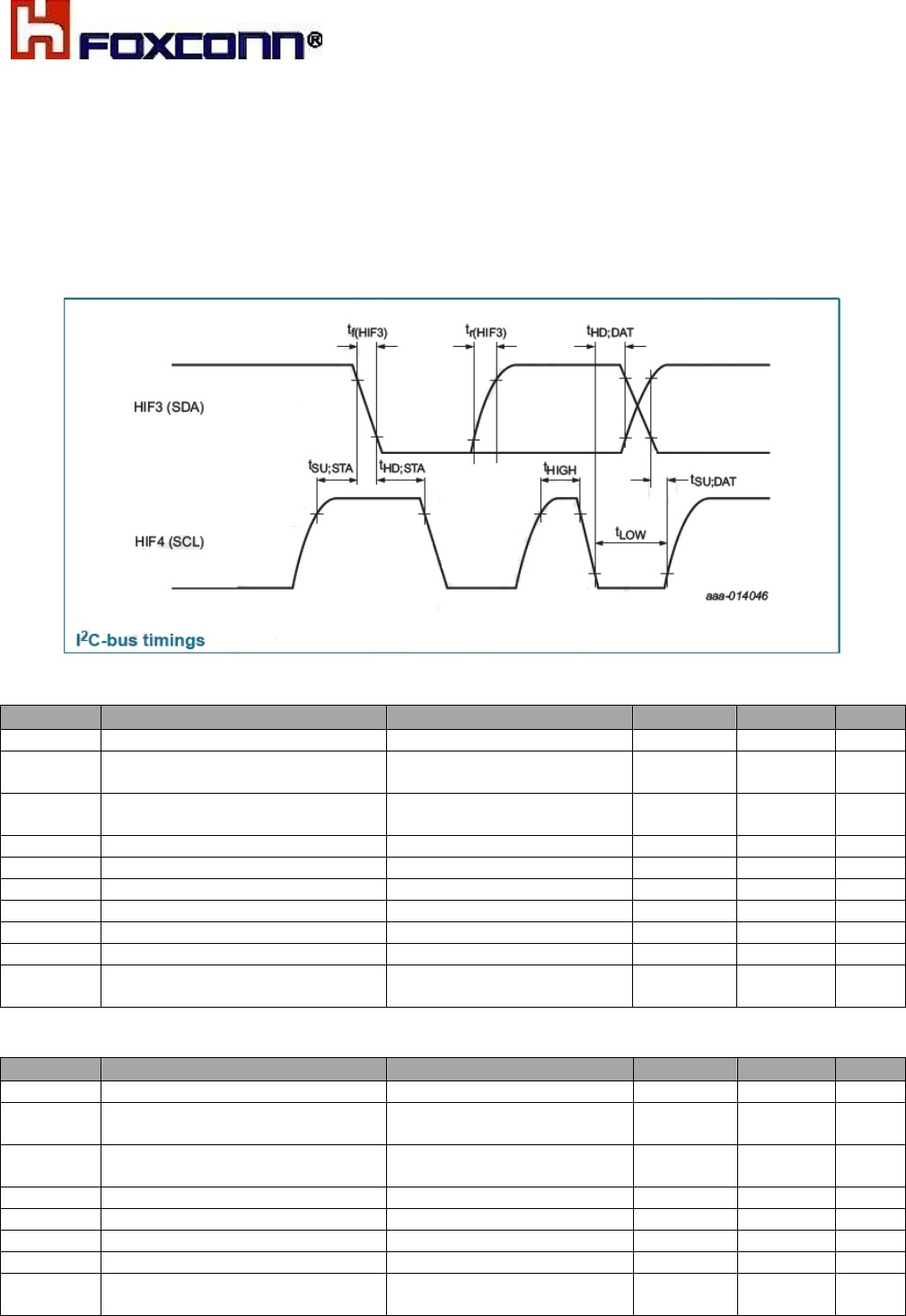
I2C-bus Interface
The I2C-bus Interface implements a slave I2C-bus interface with integrated shift register, shift timing generation
and slave address recognition.
I2C-bus Standard mode (100 KHz SCL), Fast mode (400 KHz SCL) and High-speed mode (3.4 MHz SCL) are
supported.
I2C-bus timings
Here below are timings and frequency specifications.
High-speed mode I2C-bus timing specification
Symbol
Parameter
Conditions
Min
Max
Unit
fCLK(HIF4)
Clock frequency on pin HIF4
I2C-bus SCL; C <100pF
b
0
3.4
MHz
tSU;STA
Set-up time
for a
repeated
START condition
Cb<100pF
160
-
ns
tHD;STA
Hold time(repeated) START
condition
Cb<100pF
160
-
ns
tLOW
LOW period of the SCL clock
Cb<100pF
160
-
ns
tHIGH
HIGH period of the SCL clock
Cb<100pF
60
-
ns
tSU;DAT
Date set-up time
Cb<100pF
10
-
ns
tHD;DAT
Data hold time
Cb<100pF
0
-
ns
tr(HIF3)
Rise time on pin HIF3
I2C-bus SDA; C <100pF
b
10
80
ns
tf(HIF3)
Fall time on pin HIF3
I2C-bus SDA; C <100pF
b
10
80
ns
Vhys
Hysteresis voltage
Schmitt
trigger inputs;
Cb<100pF
0.1*VPVDD
-
V
Fast mode I2C-bus timing specification
Symbol
Parameter
Conditions
Min
Max
Unit
fCLK(HIF4)
Clock frequency on pin HIF4
I2C-bus SCL; C <400pF
b
0
400
KHz
tSU;STA
Set-up time
for a
repeated
START condition
Cb<400pF
600
-
ns
tHD;STA
Hold time(repeated) START
condition
Cb<400pF
600
-
ns
tLOW
LOW period of the SCL clock
Cb<400pF
1.3
-
ns
tHIGH
HIGH period of the SCL clock
Cb<400pF
600
-
ns
tSU;DAT
Date set-up time
Cb<400pF
100
-
ns
tHD;DAT
Data hold time
Cb<400pF
0
900
ns
Vhys
Hysteresis voltage
Schmitt
trigger inputs;
Cb<400pF
0.1* VPVDD
-
V
COMPANY
CONFIDENTIAL
8
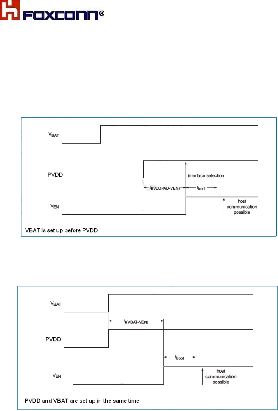
2.2 Power-up sequence
There are 2 different supplies for module which allows set up independently, therefore
different power-up sequences have to be considered.
1> VBAT is set up before PVDD
This is at least the case when VBAT pin is directly connected to the battery and when
module VBAT is always supplied as soon the system is supplied.
As VEN pin is referred to VBAT pin, VEN voltage shall go high after VBAT has been set.
2> PVDD and VBAT are set up in the same time
It is at least the case when VBAT pin is connected to a PMU/regulator which also supplies
PVDD.
9
COMPANY
CONFIDENTIAL
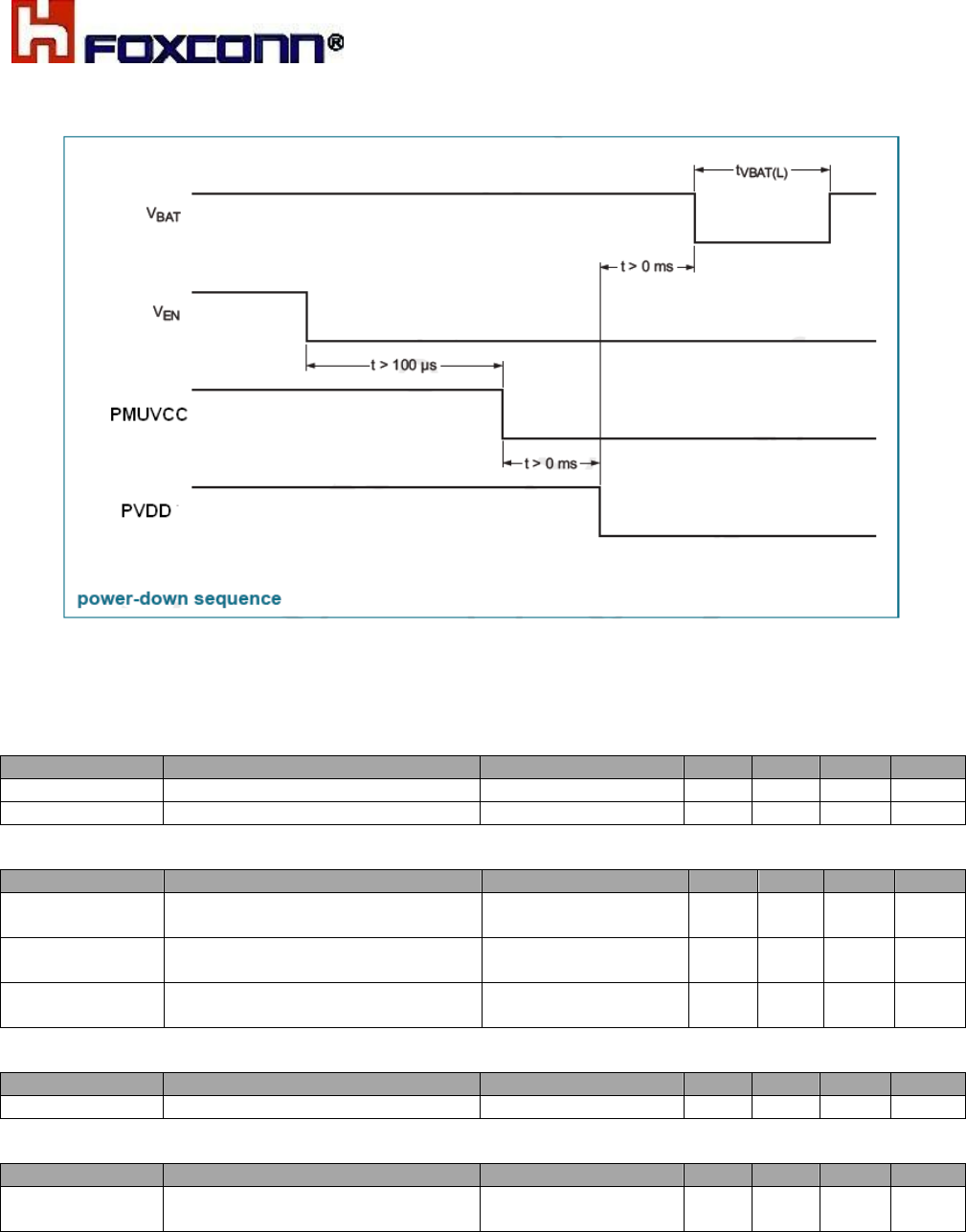
2.3 Power-down sequence
2.4 Function timing characteristics
Reset timing
Symbol
Parameter
Conditions
Min
Typ
Max
Unit
tW(VEN)
VEN pulse width
To reset
10
-
-
us
tboot
Boot time
-
-
2.5
ms
Power-up timings
Symbol
Parameter
Conditions
Min
Typ
Max
Unit
t
t(V
BAT
-VEN)
Transition time from pin VBAT to
pin VEN
VBAT,VEN
Voltage=HIGH
0
0.5
-
ms
t
t(V
PVDD
-VEN)
Transition time from pin PVDD to
pin VEN
PVDD,VEN
Voltage=HIGH
0
0.5
-
ms
t
t(V
BAT
-V
PVDD
)
Transition time from pin VBAT to
pin PVDD
VBAT,PVDD
Voltage=HIGH
0
0.5
-
ms
Power-down timings
Symbol
Parameter
Conditions
Min
Typ
Max
Unit
tVBAT(L)
Time VBAT LOW
20
-
-
ms
Download mode timings
Symbol
Parameter
Conditions
Min
Typ
Max
Unit
Tt(DWL_REQ-VEN)
Transition
time
from pin
DWL_REQ to pin VEN
DWL_REQ,VEN
voltage=HIGH
0
0.5
-
ms

COMPANY
CONFIDENTIAL
10
3.
NFC contactless standard conformance
3.1 Frequency interoperability
When in communication, NFC module is generating some RF frequencies. It is also sensitive
to some RF signals as it is looking from data in the field.
In order to avoid interference with others RF communication, it is required to tune the
antenna matching for antenna board.
(Remark: The antenna matching tuning is responsible for antenna vendor)
It must limit the RF frequency dispersion to 13.56MHz +/-50ppm.
3.2 Supported smart card types
Card Types
Read CSN
(Card Serial Number)
Read/Write
application data area
Supported
baud rates
NFC Forum Type1 Tag
Yes
Yes
106 kbps
NFC Forum Type2 Tag
Yes
Yes
106 kbps
NFC Forum Type3 Tag
Yes
Yes
212, 424 kbps
NFC Forum Type4 Tag
Yes
Yes
106 kbps
NFC Forum TypeV Tag
Yes
Yes
106 kbps
ISO/IEC 14443
Type
A
compliance cards
Yes
Yes (with application)
106 kbps
Mifare Classics 1K,4K
Yes
Yes (with application)
106 kbps
Mifare DESFire
Yes
Yes (with application)
106 kbps
Mifare Ultralight
Yes
Yes (with application)
106 kbps
Mifare Plus
Yes
Yes (with application)
106 kbps
(Mifare) SmartMX
Yes
Yes (with application)
106 kbps
ISO/IEC 14443
Type
B
compliance cards
Yes
Yes (with application)
106 kbps
FeliCa general card
Yes
Yes (with application)
212, 424 kbps
FeliCa Edy card
Yes
Yes (with application)
212, 424 kbps
FeliCa Suica card
Yes
Yes (with application)
212, 424 kbps
FeliCa PKI Option card
Yes
Yes (with application)
212, 424 kbps
HID iCLASS Seos
Yes
Yes (with application)
106 kbps

COMPANY
CONFIDENTIAL
11
3.3 Contactless interface unit
The NFC module supports various communication modes at different transfer speeds and
modulation schemes. The following chapters give more detailed overview of selected
communication modes.
1> Reader/Writer communication modes
Generally 5 reader/writer communication modes are supported:
•
PCD reader/writer for ISO/IEC 14443A/MIFARE
The transfer speed includes 106 kbit/s, 212 kbit/s, 424 kbit/s and 848 kbit/s.
•
PCD reader/writer for ISO/IEC 14443B
The transfer speed includes 106 kbit/s, 212 kbit/s, 424 kbit/s and 848 kbit/s.
•
PCD reader/writer for Jewel/Topaz tags
The transfer speed includes 106 kbit/s, 212 kbit/s, 424 kbit/s and 848 kbit/s.
•
PCD reader/writer for FeliCa cards
The transfer speed includes 212 kbit/s, 424 kbit/s.
•
VCD reader/writer for ISO/IEC 15693/ICODE
The transfer speed includes 1.65 kbit/s, 26.48 kbit/s.
2> Peer to Peer communication modes
(ISO/IEC 18092, Ecma 340 NFCIP-1 communication modes)
An NFCIP-1 communication takes place between 2 devices:
•
NFC initiator: generates RF field at 13.56 MHz and starts the NFCIP-1communication.
•
NFC Target: responds to NFC initiator command either in a load modulation scheme in Passive
communication mode or using a self-generated and self-modulated RF field for Active communication
mode.
The NFCIP-1 communication differentiates between Active and Passive communication
modes.
•
Active communication mode means both the NFC initiator and the NFC target are using their own RF field
to transmit data
•
Passive communication mode means that the NFC target answers to an NFC initiator command in a load
modulation scheme. The NFC initiator is active is terms of generating the RF field.
The NFC module supports the Active Target, Active Initiator, Passive Target and Passive
Initiator communication modes at the transfer speeds 106 kbit/s, 212 kbit/s and 424 kbit/s.
3> Card communication modes
The NFC module can be addressed as an ISO/IEC 14443A or ISO/IEC 14443B cards. This
means that NFC module can generate an answer in a load modulation scheme.
The transfer speed includes 106 kbit/s, 212 kbit/s and 424 kbit/s.
COMPANY
CONFIDENTIAL
12
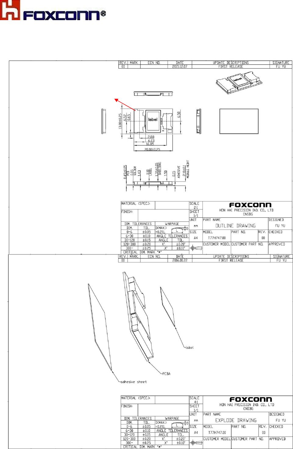
4.
Mechanical Architecture
4.1 Module Mechanical Drawing
Dimension (WxL): 20mm x 13mm, Module Max Thickness: 2.2mm
Pin 1
13
COMPANY
CONFIDENTIAL
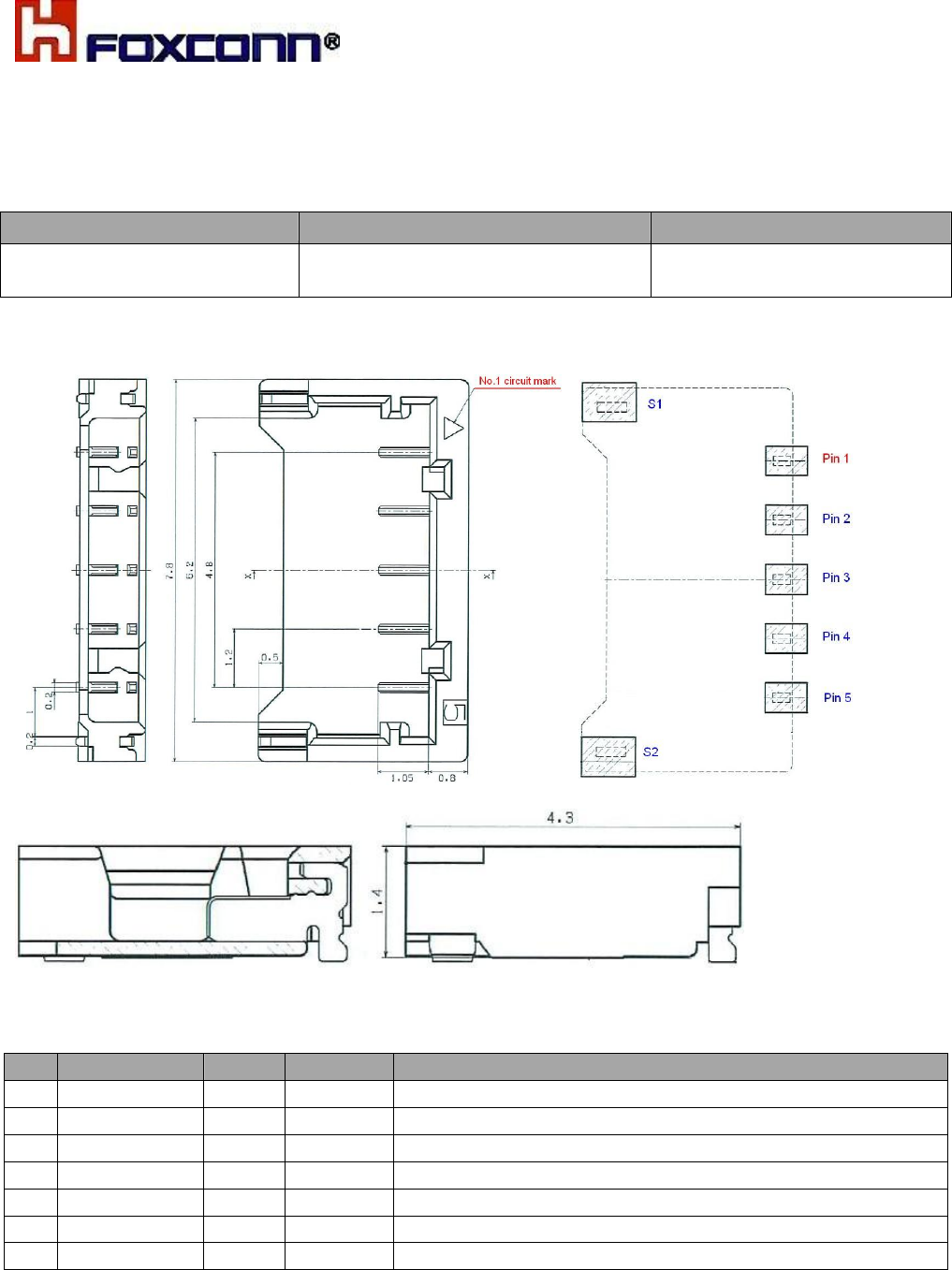
4.2 Antenna interface of NFC module
1> Antenna connector
Manufacturer: JST Manufacturer PN: BM05B-ACHKS-A-GAN-ETF(HF)
Connector Type
Manufacture PN
Size
ACH connector SMT type with
1.2mm pitch
JST : BM05B-ACHKS-A-GAN-
ETF(HF)
7.8mm x 4.3mm x 1.5mm
Connector 2D drawing:
Remark: Dimension Tolerance: +/-0.3mm
Pin definition:
Pin
Symbol
I/O
Refer
Note
1
RXP
I
VDD
Positive receiver input
2
TX1
O
VDD
Antenna output1
3
GND
G
N/A
Ground
4
TX2
O
VDD
Antenna output2
5
RXN
I
VDD
Negative receiver input
S1
GND
G
N/A
Ground
S2
GND
G
N/A
Ground
Remark: P = power supply, G = ground, I = input, O = output, I/O = input/output
14
COMPANY
CONFIDENTIAL
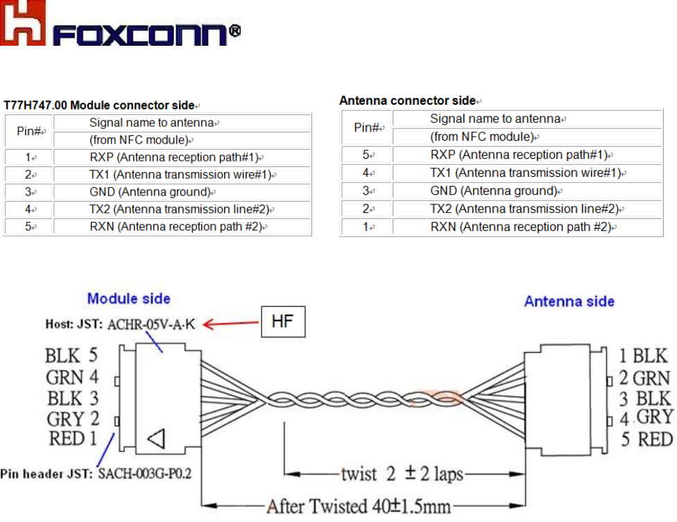
2> Recommend Antenna cable design.
15
COMPANY
CONFIDENTIAL
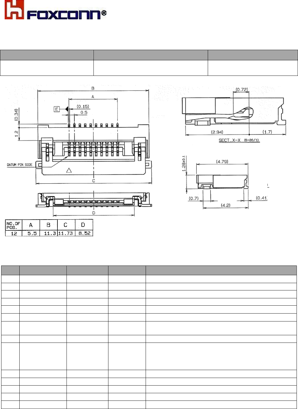
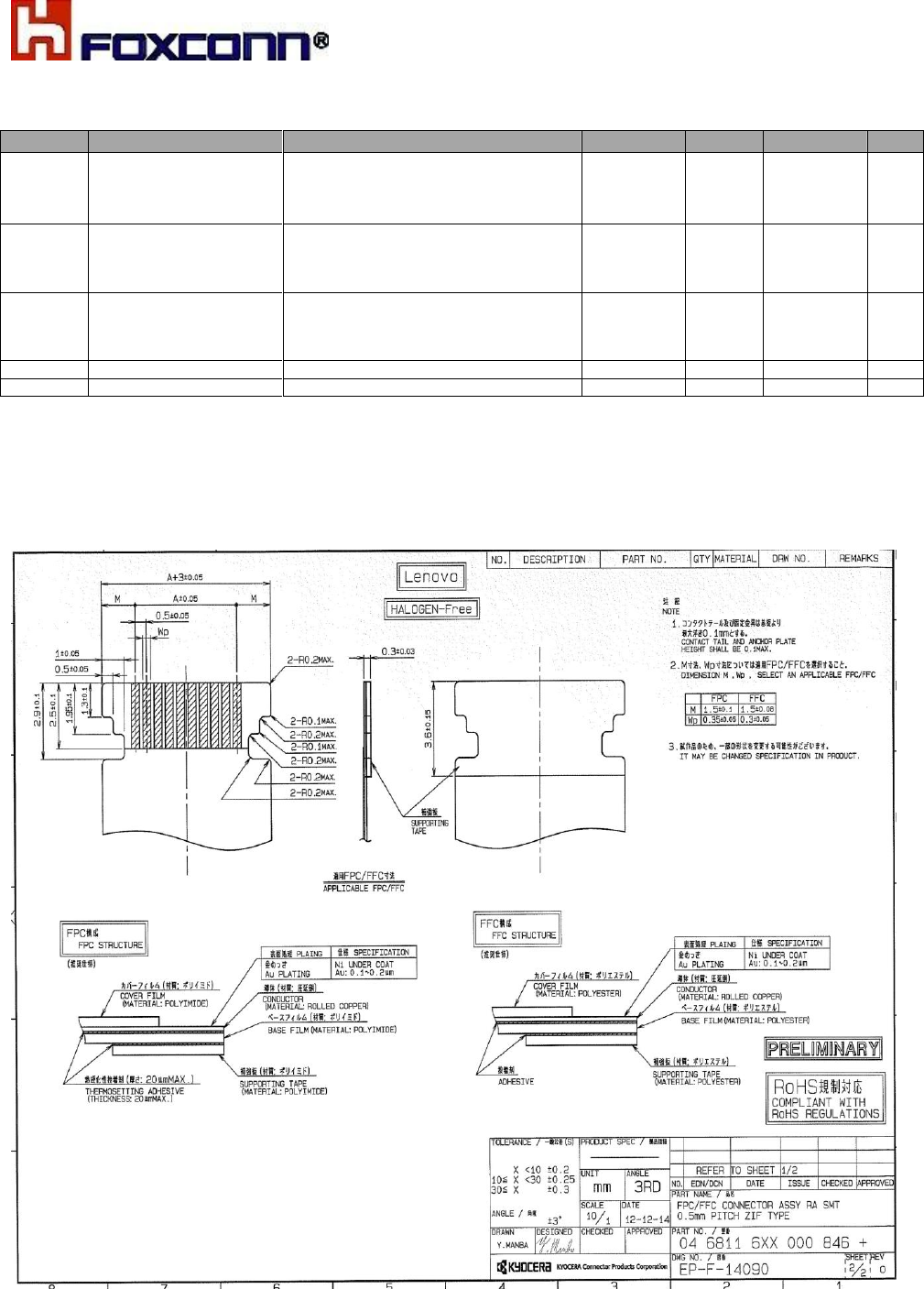
4.3. Host interface of NFC module
1> Host interface connector
Manufacturer: KYOCERA Manufacturer PN: 046811612000846 +
Connector
Manufacture PN
Size
FPC/FFC connector SMT type
with 0.5mm pitch
KYOCERA: 046811612000846+
11.73mm x 4.79mm x 1.28mm
Remark: The connector is bottom conduct with golden plating of FPC cable
Pin
Symbol
Pin Type
Refer
Description
1
VBAT
Input Power
N/A
Power supply from system (4.5V - 5.5V)
2
PVDD
Input Power
N/A
Power supply to I/O (3.0V – 3.6V)
3
I2C_SDA
I/O
PVDD
I2C data
4
I2C _SCL
I
PVDD
I2C clock
5
GND
G
N/A
Ground
6
IRQ
O
PVDD
Interrupt from NFC module to the host (Host_Wake)
7
NFC_Presence
G
N/A
Connect to ground for NFC module presence bit (Low
active)
8
VEN
I
VBAT
Reset pin. Set the device in Hard Power Down
9
TX_PWR_REQ
O
VDD
(External TX power supply request)
(Active high 1.8V level output)
Indicates NFC busy state during NFC communication
to touchpad.
10
PMUVCC
Input Power
N/A
Power supply to UICC(1.78V~3.3V)
11
SWIO_UICC
I/O
VDD(SIM)
SWP data connection to SIM
12
DWL_REQ
I
PVDD
Firmware download control pin
S1
GND
G
N/A
Ground
S2
GND
G
N/A
Ground
Remark: P = power supply, G = ground, I = input, O = output, I/O = input/output
Pin
1
16
COMPANY
CONFIDENTIAL
2> Pin characteristics
VEN input pin characteristics
Symbol
Parameter
Conditions
Min
Typ
Max
Unit
VIH
HIGH-level input voltage
1.1
-
VBAT
V
VIL
LOW-level input voltage
0
-
0.4
V
IIH
HIGH-level input current
VEN voltage=VBAT
-
-
1
µA
IIL
LOW-level input current
VEN voltage=0V
1
-
-
µA
Ci
Input capacitance
-
5
-
pF
Pin characteristics for IRQ, and TX_PWR_REQ
[1] Activated in HPO and Monitor states.
Input pin characteristics for DWL_REQ
Symbol
Parameter
Conditions
Min
Typ
Max
Unit
VIH
HIGH-level input voltage
VPVDD=1.8V
0.65*VPVDD
-
-
V
VIL
LOW-level input voltage
V PVDD=1.8V
-
-
0.35*VPVDD
V
VIH
HIGH-level input voltage
VPVDD=3V
2
-
-
V
VIL
LOW-level input voltage
VPVDD=3V
-
-
0.8
V
IIH
HIGH-level input current
-
-
1
µA
IIL
LOW-level input curent
1
-
-
µA
Ci
Input capacitance
-
5
-
pF
Rpd
Pull down resistance
Extra pull-down
0.35
-
0.85
MΩ
Pin characteristics for HIF3(used as I2C-bus SDA) and HIF4(used as I2C-bus SCL)
[1] Only for pin HIF3(I2C-bus SDA), HIF4(I2C-bus SCL) is only used as input.
Symbol
Parameter
Conditions
Min
Typ
Max
Unit
VOH
HIGH-level output voltage
IOH<3mA
-
-
-
-
IRQ and CLK_REQ pin
VPVDD -0.4
-
VPVDD
V
TX_PWR_REQ pin
VDD-0.4
-
VDD
V
VOL
LOW-level output voltage
IOL<3mA
0
-
0.4
V
CL
Load capacitance
-
-
20
pF
tf
Fall time
CL=12pF max
High speed
1
-
3.5
ns
Low speed
2
-
10
ns
tr
Rise time
CL=12pF max
High speed
1
-
3.5
ns
Low speed
2
-
10
ns
Rpd
Pull-down resistance
IRQ and CLK_REQ pins [1]
0.35
-
0.85
M
Ω
TX_PWR_REQ pin [1]
55
-
120
k
Ω
Symbol
Parameter
Conditions
Min
Typ
Max
Unit
VOL
LOW-level output voltage
IOL<3mA [1]
0
-
0.4
V
CL
Load capacitance
-
-
10
pF
tf
Fall time
CL=100 pF; [1]
Rpull-up=2k
Ω
; Standard and Fast mode
30
-
250
ns
CL=100 pF; [1]
Rpull-up=1k
Ω
; High-speed mode
80
-
110
ns
tr
Rise time
CL=100 pF; [1]
Rpull-up=2k
Ω
; Standard and Fast mode
30
-
250
ns
CL=100 pF; [1]
Rpull-up=1k
Ω
; High-speed mode
10
-
100
ns
VIH
HIGH-level input voltage
0.7 *VPVDD
-
VPVDD
V
VIL
LOW-level input voltage
0
-
0.3*VPVDD
V
IIH
HIGH-level input current
VI= VPVDD; high impedance
-
-
1
µA
IIL
LOW-level input current
VI=0V; high impedance
-1
-
-
µA
Ci
Input capacitance
-
5
-
pF
17
COMPANY
CONFIDENTIAL
SWIO_UICC pin characteristics
[1] To allow for overshoot, the voltage on SWIO shall remain between -0.3V and V +0.3V during dynamic
operation.
3> Recommend FPC cable
OHmax
.
Symbol
Parameter
Conditions
Min
Typ
Max
Unit
VOH
HIGH-level output voltage
IIH=1mA; [1]
IDD(SIM)=50mA;
VDD(SIM_PMU)=2.75V;
VDD(SIM_PMU) in class B
1.4
-
-
V
VOH
HIGH-level output voltage
ISIM_SWIO=1mA; [1]
IDD(SIM)=30mA;
VDD(SIM_PMU)=1.67V;
VDD(SIM_PMU) in class C
0.85 VDD(SIM)
-
-
V
VOH
HIGH-level output voltage
IIH =1mA; [1]
IDD(SIM)=5mA;
VDD(SIM_PMU)=0V;
VDD(SIM)-VDDD
0.85 VDD(SIM)
-
-
V
VOL
LOW-level output voltage
0µA<IIL<20Μa [1]
-
-
0.15VDD(SIM)
V
IIH
HIGH-level input current
-
300
-
µA
18
COMPANY
CONFIDENTIAL
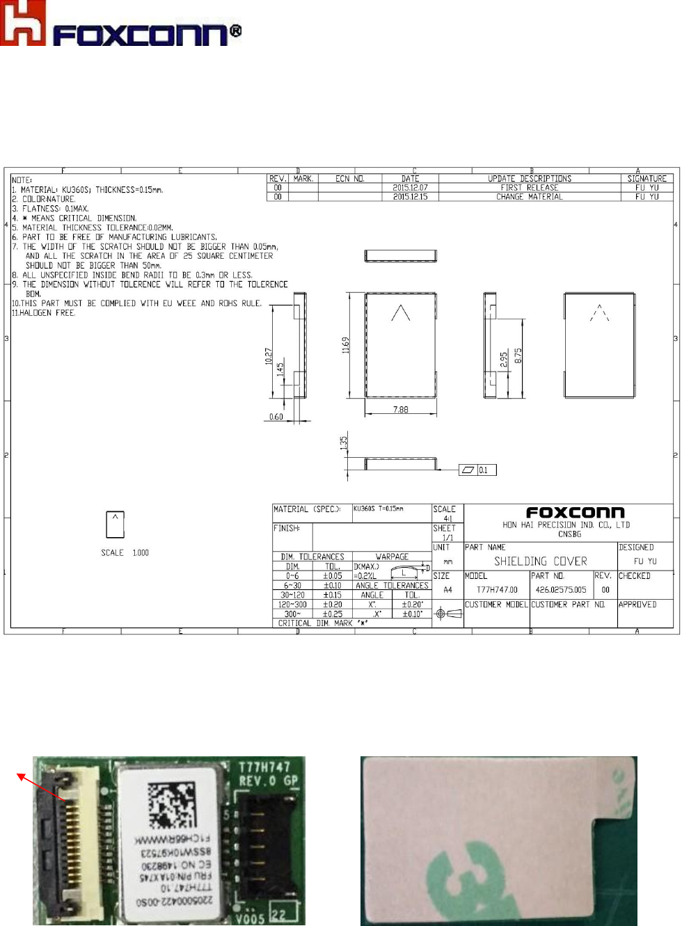
4.4. Shielding Cover of NFC module
Dimension (L x W x H): 11.69mm x 7.88mm x 1.35mm, Thickness: 0.15mm
Materials: KU360S
4.5. Picture of NFC module
(Top view) (Bottom view)
Pin 1
COMPANY
CONFIDENTIAL
21
7.
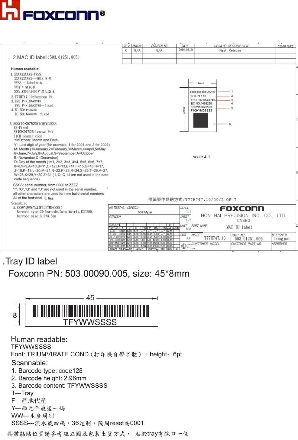
Marking Information
Label information
22
COMPANY CONFIDENTIAL
23
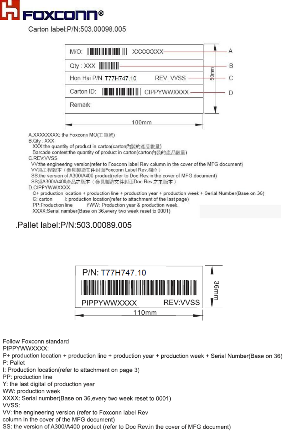
8.
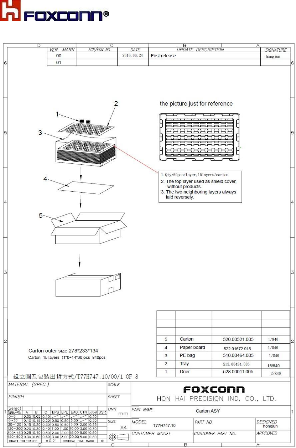
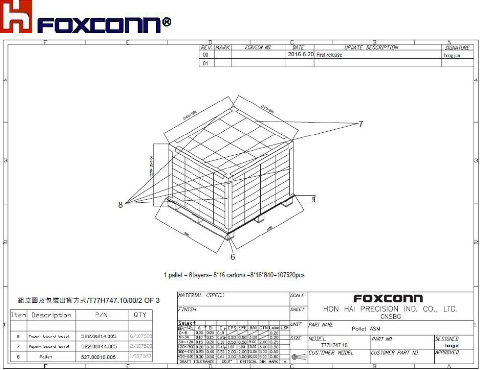
Packing information COMPANY CONFIDENTIAL
24
COMPANY
CONFIDENTIAL
25
COMPANY
CONFIDENTIAL
9.
Reliability Test plan
℃℃℃
℃
℃
℃
℃
℃℃
℃
:
No
Item
Test
Condition
Qty
Criteria
Result
1
Pull
test
&
Cross
1.
Visual
inspection:
All
locations
1. Visual
Inspection
–
Compliance
with
IPC-A-610D
Class
3
&
39T0261;
2. Function
test
Pass;
3. Cross
section
- No
separation
- Allowable
Crack
Length:
Max.
25%
of
pad
diameter
4.
Pull
test
-
800g
for
0.4mm
pitch
QFP,
1kg
for
0.5mm
pitch
QFP
TBD
2.
Cross
section:
Section
(2pcs)
BGA/Connector/PTH
Hole/Via
Cross
Section:
1pcs
Hole
(SMT/PIH)
Pull
Test:
1pcs
3.
Pull
strength:
0.4mm/0.5mm
pitch
QFP
2
Low
Temperature
Test
4.
Power
on;
5.
Temp.=
-40
;
6.
Test
Period
=
240hrs.
2
Pls
refer
to
ATC
TBD
3
Hot
Start
Test
1.Power
Off
,
2.Temperature=100
3.Test
period=96
Hours
4.Power
on
3times
2
1.
2.
Visual
Inspection
–
Compliance
with
IPC-A-
610D
Class
3
&
39T0261;
Function
test
Pass.
TBD
4
Cold
Start
Test
1.Power
Off
2.Temperature=0
3.Test
period=96
Hours
4.Power
on
3times
2
1. Visual
Inspection
–
Compliance
with
IPC-A-610D
Class
3
&
39T0261;
2. Function
test
Pass.
TBD
5
Temperature-Humidity
Bias
(THB)
1.
Power
On(
apply
core
voltage
to
PCBA
)
2.
Temp.=
85
&
Humi.=
85%R.H
3.
Test
period=
400
Hours
2
Pls
refer
to
ATC
TBD
6
Accelerated
Thermal
Cycles
(ATC)
ATC:
1. Power
off
2. Ta=85
for
7.5mins
3.Ta=85
to
-40
for
7.5mins
4.Ta=-40
for
7.5mins
5.Ta=-40
to
85
for
7.5mins
6.Repeat
630cycles
Cross
Section(both
Bright
&
Dark):
BGA/CONNECTOR/PTH
Hole/
Via
Hole
(SMT/PIH)
2
1. Visual
Inspection
–
Compliance
with
IPC-A-610D
Class
3
&
39T0261;
2. Function
test
Pass;
3. Cross
section
(
AFTER
630
cycles
)
- No
separation
- Allowable
Crack
Length:
Max.
25%
of
pad
diameter
TBD
7
Sine
Vibration(Unpackaged
)
1. Freq
:
uency
=
5
~
500
~
5
HZ;
2. Acceleration
=
2
G;
3. Sweep
time:
3mins/cycle;
4. Each
of
x,
y,
z
axis/
30
min;
5. Power
on
and
continuously
ping
AP/SG./Golden(AP
for
WLAN,
SG
for
WWAN,
Golden
for
BT)
6. Product
need
to
be
connected
with
the
mating
connector
which
used
in
laptop.
2
1. Visual
Inspection
–
Compliance
with
IPC-A-610D
Class
3
&
39T0261;
2. Function
test
Pass;
3. No
disconnect
between
device
&
AP/SG
/Golden
during
the
test
.
TBD
8
Shock
Test(Unpackaged)
1. Half-Sine
wave
,50G
,
11msec
2. Test
+/-
x,
y,
z
axes
3. Three
shock
per
axes,
total
18
shocks.
4. Product
need
to
be
connected
with
the
mating
connector
which
used
in
laptop.
5. Detect
by
an
electrical
discontinuity
monitor.
2
1. Visual
Inspection
–
Compliance
with
IPC-A-610D
Class
3
&
39T0261;
2. No
electrical
discontinuity
is
greater
than
1
microsecond.
TBD
9
Sine
Vibration(Packaged)
1. Frequency
=
5
~
500
~
5
HZ;
2. Acceleration
=
2
Grms;
3. Each
of
x,
y,
z
axis/
30
mins.
1
Carton
1. Visual
Inspection
–
Compliance
with
IPC-A-610D
Class
3
&
39T0261;
2. Function
test
Pass.
TBD
10
Shock
Test(Packaged)
1. Sine
wave
,230G
,
3msec
;
2. Test
+/-
x,
y,
z
axes
1
Carton
1. Visual
Inspection
–
Compliance
with
IPC-A-610D
Class
3
&
39T0261;
2. Function
test
Pass.
TBD
11
Tin
Wisker
1. Power
off
60/95%RH
for
2000hrs;
2. Room
Temperature
2000hrs.
10
Whisker
Length
<50um
TBD

26
COMPANY
CONFIDENTIAL
10.
Notice
Operating Temperature Conditions
The product shall be capable of continuous reliable operation when operating in ambient
temperature of 0°C to 70°C.
Non-Operating Temperature Conditions
Neither subassembly shall be damaged nor shall the operational performance be degraded
when restored to the operating temperature when exposed to storage temperature in the
range of -20°C to +85°C.
Operating Humidity Conditions
The product shall be capable of continuous reliable operation when subjected to relative
humidity in the range of 0% and 85% non-condensing.
Handling Environment
Please make sure to avoid mechanical shock and vibration for this module.
Please do not drop the module.
Please do not clean the module.
Federal Communication Commission Interference Statement
This device complies with Part 15 of the FCC Rules. Operation is subject to the following two
conditions: (1) This device may not cause harmful interference, and (2) this device must accept any
interference received, including interference that may cause undesired operation.
This equipment has been tested and found to comply with the limits for a Class B digital device,
pursuant to Part 15 of the FCC Rules. These limits are designed to provide reasonable protection
against harmful interference in a residential installation. This equipment generates, uses and can
radiate radio frequency energy and, if not installed and used in accordance with the instructions, may
cause harmful interference to radio communications. However, there is no guarantee that
interference will not occur in a particular installation. If this equipment does cause harmful
interference to radio or television reception, which can be determined by turning the equipment off
and on, the user is encouraged to try to correct the interference by one of the following measures:
−
Reorient or relocate the receiving antenna.
−
Increase the separation between the equipment and receiver.
−
Connect the equipment into an outlet on a circuit different from that
to which the receiver is connected.
−
Consult the dealer or an experienced radio/TV technician for help.
FCC Caution: Any changes or modifications not expressly approved by the party responsible for
compliance could void the user's authority to operate this equipment.
This transmitter must not be co‐located or operating in conjunction with any other antenna or
transmitter.
Radiation Exposure Statement:
This equipment complies with FCC radiation exposure limits set forth for an uncontrolled environment.
This equipment should be installed and operated with minimum distance 20cm between the radiator
& your body.

This device is intended only for OEM integrators under the following conditions:
The antenna must be installed such that 20 cm is maintained between the antenna and users, and
The transmitter module may not be co‐located with any other transmitter or antenna.
As long as 2 conditions above are met, further transmitter test will not be required. However, the OEM
integrator is still responsible for testing their end‐product for any additional compliance requirements
required with this module installed
IMPORTANT NOTE: In the event that these conditions can not be met (for example certain laptop
configurations or co‐location with another transmitter), then the FCC authorization is no longer
considered valid and the FCC ID can not be used on the final product. In these circumstances, the OEM
integrator will be responsible for re‐evaluating the end product (including the transmitter) and
obtaining a separate FCC authorization.
End Product Labeling
This transmitter module is authorized only for use in device where the antenna may be installed such
that 20 cm may be maintained between the antenna and users. The final end product must be labeled
in a visible area with the following: “Contains FCC ID:MCLT77H747”. The grantee's FCC ID can be used
only when all FCC compliance requirements are met.
Manual Information To the End User
The OEM integrator has to be aware not to provide information to the end user regarding how to
install or remove this RF module in the user’s manual of the end product which integrates this
module.
The end user manual shall include all required regulatory information/warning as show in this manual.
Industry Canada statement:
This device complies with ISED’s licence‐exempt RSSs. Operation is subject to the following two
conditions: (1) This device may not cause harmful interference, and (2) this device must accept any
interference received, including interference that may cause undesired operation.
Le présent appareil est conforme aux CNR d’ ISED applicables aux appareils radio exempts de licence.
L’exploitation est autorisée aux deux conditions suivantes : (1) le dispositif ne doit pas produire de
brouillage préjudiciable, et (2) ce dispositif doit accepter tout brouillage reçu, y compris un brouillage
susceptible de provoquer un fonctionnement indésirable.
Radiation Exposure Statement:
This equipment complies with ISED radiation exposure limits set forth for an uncontrolled
environment. This equipment should be installed and operated with minimum distance 20cm
between the radiator & your body.
Déclaration d'exposition aux radiations:
Cet équipement est conforme aux limites d'exposition aux rayonnements ISED établies pour un
environnement non contrôlé. Cet équipement doit être installé et utilisé avec un minimum de 20 cm
de distance entre la source de rayonnement et votre corps.
This device is intended only for OEM integrators under the following conditions: (For module device
use)
1) The antenna must be installed such that 20 cm is maintained between the antenna and users, and
2) The transmitter module may not be co‐located with any other transmitter or antenna.
As long as 2 conditions above are met, further transmitter test will not be required. However, the OEM
integrator is still responsible for testing their end‐product for any additional compliance requirements
required with this module installed.
Cet appareil est conçu uniquement pour les intégrateurs OEM dans les conditions suivantes: (Pour
utilisation de dispositif module)
1) L'antenne doit être installée de telle sorte qu'une distance de 20 cm est respectée entre l'antenne
et les utilisateurs, et 2) Le module émetteur peut ne pas être coïmplanté avec un autre émetteur ou
antenne.
Tant que les 2 conditions ci‐dessus sont remplies, des essais supplémentaires sur l'émetteur ne seront
pas nécessaires. Toutefois, l'intégrateur OEM est toujours responsable des essais sur son produit final
pour toutes exigences de conformité supplémentaires requis pour ce module installé.
IMPORTANT NOTE:
In the event that these conditions can not be met (for example certain laptop configurations or
co‐location with another transmitter), then the Canada authorization is no longer considered valid and
the IC ID can not be used on the final product. In these circumstances, the OEM integrator will be
responsible for re‐evaluating the end product (including the transmitter) and obtaining a separate
Canada authorization.
NOTE IMPORTANTE:
Dans le cas où ces conditions ne peuvent être satisfaites (par exemple pour certaines configurations
d'ordinateur portable ou de certaines co‐localisation avec un autre émetteur), l'autorisation du
Canada n'est plus considéré comme valide et l'ID IC ne peut pas être utilisé sur le produit final. Dans
ces circonstances, l'intégrateur OEM sera chargé de réévaluer le produit final (y compris l'émetteur) et
l'obtention d'une autorisation distincte au Canada.
End Product Labeling
This transmitter module is authorized only for use in device where the antenna may be installed such that 20 cm may
be maintained between the antenna and users. The final end product must be labeled in a visible area with the
following: “Contains IC: 2878D-T77H747”.
Plaque signalétique du produit final
Ce module émetteur est autorisé uniquement pour une utilisation dans un dispositif où l'antenne peut être installée
de telle sorte qu'une distance de 20cm peut être maintenue entre l'antenne et les utilisateurs. Le produit final doit
être étiqueté dans un endroit visible avec l'inscription suivante: "Contient des IC: 2878D-T77H747".
Manual Information To the End User
The OEM integrator has to be aware not to provide information to the end user regarding how to install or remove
this RF module in the user’s manual of the end product which integrates this module.
The end user manual shall include all required regulatory information/warning as show in this manual.
Manuel d'information à l'utilisateur final
L'intégrateur OEM doit être conscient de ne pas fournir des informations à l'utilisateur final quant à la façon d'installer
ou de supprimer ce module RF dans le manuel de l'utilisateur du produit final qui intègre ce module.
Le manuel de l'utilisateur final doit inclure toutes les informations réglementaires requises et avertissements comme
indiqué dans ce manuel.
This radio transmitter (IC: 2878D-T77H747, Model: T77H747) has been approved by Industry Canada to operate with
the antenna types listed below with the maximum permissible gain indicated. Antenna types not included in this list,
having a gain greater than the maximum gain indicated for that type, are strictly prohibited for use with this device.
Cet émetteur radio (IC: 2878D-T77H747, Modèle: T77H747) a été approuvé par Industrie Canada pour fonctionner
avec les types d'antenne énumérés ci-dessous avec le gain maximal admissible indiqué. types d'antennes non inclus
dans cette liste, ayant un gain supérieur au gain maximum indiqué pour ce type, sont strictement interdits pour une
utilisation avec cet appareil.
DETACHABLE ANTENNA USAGE
This radio transmitter (IC: 2878DT77H747 / Model: T77H747) has been approved by ISED to operate with the
antenna type listed below with maximum permissible gain indicated. Antenna types not included in this list,
having a gain greater than the maximum gain indicated for that type, are strictly prohibited for use with this
device.
Le présent émetteur radio (IC: 2878DT77H747 / Model: T77H747) a été approuvé par ISED pour fonctionner
avec les types d'antenne énumérés ci-dessous et ayant un gain admissible maximal. Les types d'antenne non
inclus dans cette liste, et dont le gain est supérieur au gain maximal indiqué, sont strictement interdits pour
l'exploitation de l'émetteur.
ġ
This radio transmitter (IC: 2878DT-77H747 / Model: T77H747) has been approved by ISED to operate with
the antenna type listed below with maximum permissible gain indicated. Antenna types not included in this
list, having a gain greater than the maximum gain indicated for that type, are strictly prohibited for use with
this device.
Le présent émetteur radio (IC: 2878D-T77H747 / Model: T77H747) a été approuvé par ISED pour fonctionner
avec les types d'antenne énumérés ci-dessous et ayant un gain admissible maximal. Les types d'antenne non
inclus dans cette liste, et dont le gain est supérieur au gain maximal indiqué, sont strictement interdits pour
l'exploitation de l'émetteur.
低功率電波輻射性電機管理辦法
第十二條 經型式認證合格之低功率射頻電機,非經許可,公司、商號或使用者均不得擅自變更 頻率、加大
功率或變更原設計之特性及功能。
第十四條 低功率射頻電機之使用不得影響飛航安全及干擾合法通信;經發現有干擾現象時,應 立
即停用,並改善至無干擾時方得繼續使用。 前項合法通信,指依電信法規定作業之無線電通信。
低功率射頻電機須忍受合法通信或工業、科學及醫療用電波輻射性電機設備之干擾。
模組認證:
1. 本模組於取得認證後將依規定於模組本體標示審驗合格標籤。
2. 系統廠商應於平台上標示「本產品內含射頻模組: XXXyyyLPDzzzz‐x」字樣。
「電磁波曝露量 MPE 標準值 1mW/cm2,送測產品實測值為 0.97 mW/cm2」