HYT Science and Technology Co TC-620U2 Two-way Radio User Manual TC 610 620 Service Manual VO1
Shenzhen HYT Science &Technology; Co Ltd Two-way Radio TC 610 620 Service Manual VO1
Contents
- 1. Service Manual
- 2. Users Manual
Service Manual

1
CONTENTS
General-------------------------------------------------------------------------------------2
Radio Overview-------------------------------------------------------------------------3
Software Specifications--------------------------------------------------------------7
Circuit Description---------------------------------------------------------------------8
Semiconductor Data----------------------------------------------------------------16
TC-610/620 Parts List 1-------------------------------------------------------------18
(U1) ……………………………………………………………….………….…………
(U2)…………………………………………………………………………….…………
Adjustment------------------------------------------------------------------------------46
Troubleshooting Flow Chart------------------------------------------------------56
Disassembly and Assembly-------------------------------------------------------55
Exploded View-------------------------------------------------------------------------64
TC-610/620 Parts List 2--------------------------------------------------------------66
Packing--------------------------------------------------------------------------------70
TC-610/620 PCB View----------------------------------------------------------------71
TC-610/620 Block Diagram---------------------------------------------------------74
TC-610/620 UHF ………………………………………………………………………………
TC-610/620 Level Diagram------------------------------------------------77
TC-610/620 Schematic Diagram--------------------------------------------------80
(U1) Schematic Diagram (AF & IF & PLL) …………………………………………………
(U1) Schematic Diagram (MCU & POWER)………………………………………….…………
(U1) Schematic Diagram (VCO & RF)………………………………………….…………
(U2) Schematic Diagram (AF & IF & PLL)…………………………………….……

2
(U2) Schematic Diagram (MCU & POWER)………………………………………….…………
(U2) Schematic Diagram (VCO & RF)………………………………………….……
Specifications-----------------------------------------------------------------------81

3
General
Manual Scope
This manual is intended for use by experienced technicians familiar with similar types of
communication equipment. It contains all service information required for the equipment and is
current as of the publication date.
Safety and General Information
The following general safety precautions as would normally apply, should be observed during all
phases of operation, service and repair of this equipment.
z This equipment should be serviced by qualified technicians only.
z DO NOT operate the transmitter of radio unless all RF connectors are secure and any open
connectors are properly terminated.
z Do not modify the radio for any reason.
z Use only HYT original batteries and chargers.
z Use only the supplied or an approved antenna.
z Do not use any portable radio that has a damaged antenna. If a damaged antenna comes into
contact with your skin, a minor burn can result.
z For vehicles with an air bag, do not place a radio in the area over an air bag or in the air bag
deployment area. Air bags inflate with great force. If a radio is placed in the air bag deployment
area and the air bag inflates, the radio may be propelled with great force and cause serious
injury to occupants of the vehicle.
z Turn off your radio prior to entering any area with a potentially explosive atmosphere.
z Do not charge your battery in a potentially explosive atmosphere.
z To avoid possible interference with blasting operations, turn off your radio when you are near
electrical blasting caps, in a blasting area, or in areas posted: “Turn off two-way radio.” Obey
all signs and instructions.
z Do not expose the radio to direct sunlight over a long time, nor place it close to heating source.
z When using your radio, hold the radio in a vertical position with the microphone 3 to 4
centimeters away from your lips.
z If you wear a radio on your body when transmitting, ensure that the radio and its antenna are at
least 2.5cm away from your body.
4
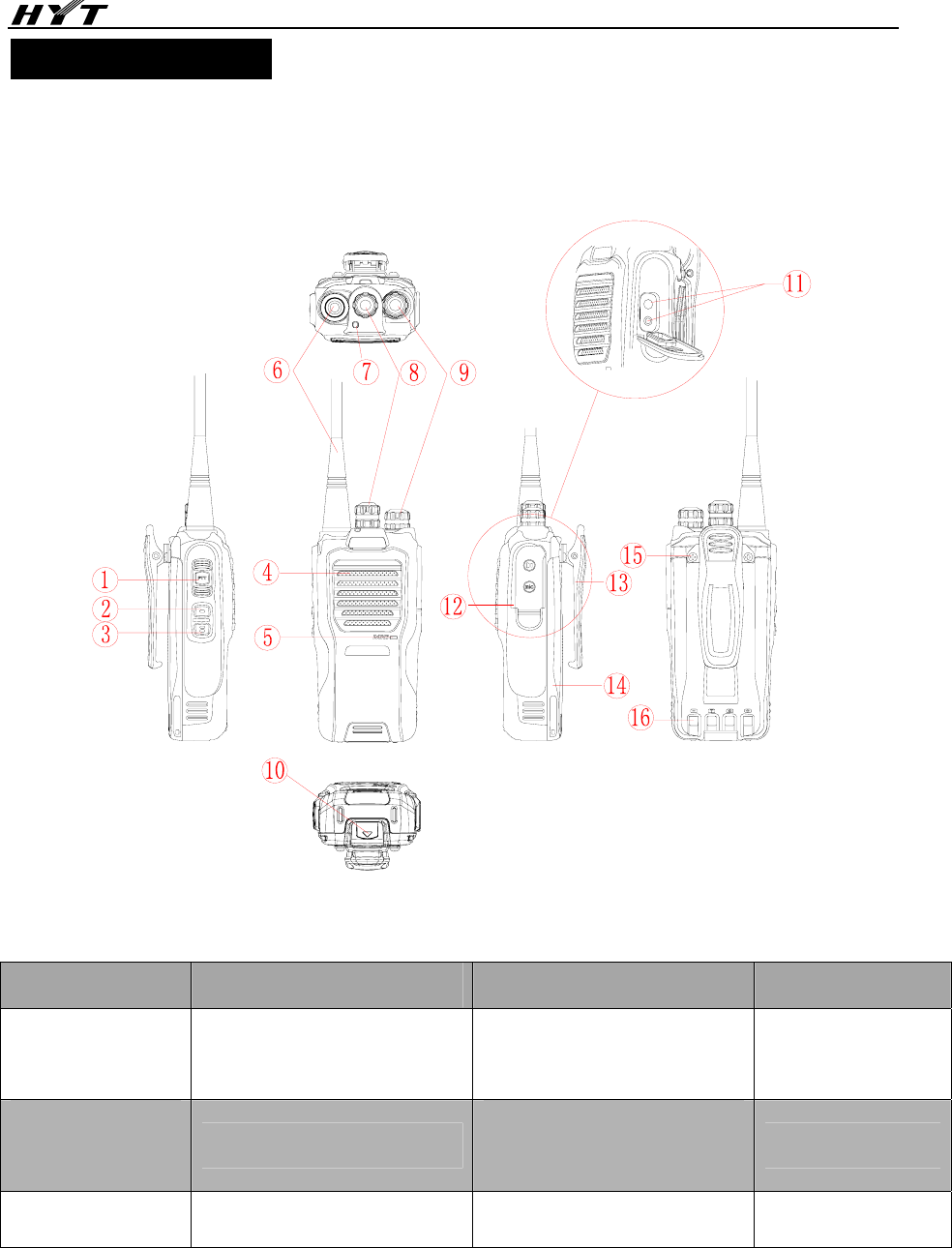
Radio Overview
TC-610
① PTT ② SK1 (programmable key) ③ SK2 (programmable key ④ Speaker
⑤ Microphone ⑥ Antenna ⑦ LED
⑧ Channel
Selector Knob
⑨ On-Off/Volume
Control Knob
⑩ Battery Latch
⑪ Earpiece Jack and
Programming Port
⑫ Earpiece Cover
⑬ Belt Clip ⑭ Battery ⑮ Belt Clip Screw ⑯ Charging Piece
5
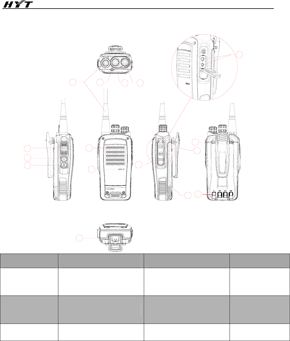
TC-620
1
2
4
5
10
678 9
12
13
14
11
3
16
15
① PTT ② SK1 (programmable key) ③ SK2 (programmable key ④ Speaker
⑤ Microphone ⑥ Antenna ⑦ LED
⑧ Channel
Selector Knob
⑨ On-Off/Volume
Control Knob
⑩ Battery Latch
⑪ Earpiece Jack and
Programming Port
⑫ Earpiece Cover
⑬ Belt Clip ⑭ Battery ⑮ Belt Clip Screw ⑯ Charging Piece
PTT
Used to switch between transmitting and receiving modes. Hold down PTT and speak into the
microphone to transmit, while release it to receive.

6
SK1
Side key 1, programmable. Your dealer can program the key with a function via the programming
software.
SK2
Side key 2, programmable. Your dealer can program the key with a function via the programming
software.
LED
LED statuses and alert tones:
Power on the source
radio while holding down
the SK2 key.
Power on the slave
radio directly.
LED flashes orange once.
Source radio (After the
slave radio is powered
on and the cloning cable
is connected, press SK2
on the source radio to
start cloning)
When cloning, LED flashes red.
When completed, red LED goes out.
When failed, red LED goes out.
User
Wired
Clone
Slave radio
When cloning, LED flashes green.
When completed, green LED goes out.
Powering On in User Mode
The power-on alert tone sounds when the radio is
powered on.
When the current channel is idle, “BEEP” tone sounds
continuously.
Low Battery Power Alert
LED flashes red and a descending tone sounds every
ten seconds.

7
Transmit
LED glows red.
When transmission times out, “BEEP” tone sounds
continuously.
TOT pre-alert: “BEEP” tone sounds once.
Receive When a carrier is received, LED glows green.
Scan
When detecting, LED flashes green every second.
Scan start tone (programmable by your dealer): “BEEP”
tone sounds once.
Scan stop tone (programmable by your dealer): “BEEP”
tone sounds once.
Priority channel scan tone (programmable by your
deader): If the radio stays on a priority channel during
receiving, “BEEP” tone sounds once.
Programming
Reading: LED flashes red.
Writing: LED flashed green.
Power Adjust
When switching from high power to low power, a
descending tone sounds.
When switching from low power to high power, an
ascending tone sounds.
VOX
When enabling the VOX function, an ascending tone
sounds.
When disabling the VOX function, a descending tone
sounds.
Channel Selector Knob
Rotate the knob to select from channels 1 to 16.
On-Off/Volume Control Knob
Rotate the knob clockwise to turn the radio on, while rotate the knob fully counter-clockwise until a
“click” is heard to turn the radio off.

8
Turn the knob clockwise to increase the volume, or counter-clockwise to decrease the volume.
Software Specifications
Functions
1. Available Channels: 1 to 16 channels
Frequency Range:
UHF: 400-420MHz
UHF: 450-470MHz
2. Channel Spacing: 25KHz/12.5KHz
3. Channel Step: 5/6.25/10/12.5KHz channel scan function
4. Tx/Rx Indication (red/green LED)
5. CTCSS/CDCSS (38 groups of CTCSS and 83 groups of CDCSS with degrees of 180/120
available for CTCSS squelch tail reverse method)
6. Low Battery Power Alert
7. Auto Battery Save
8. Unlock Detect and Alarm
9. 9 Selectable Squelch Levels
10. Monitor
11. TOT
12. Squelch Tail Elimination
13. PC Programming (including PC manual adjustment and PC automatic adjustment)
14. High/Low Power Switch (2.0/5.0W)
15. Wide/Narrow Band Compatible
16. Busy Channel Lockout
17. Wired Clone
18. Battery Power Indication
19. Manual Adjustment
20. VOX and 5 Selectable Sensitivity Levels
9
Circuit Description
Realization Methods for Basic Functional Modules
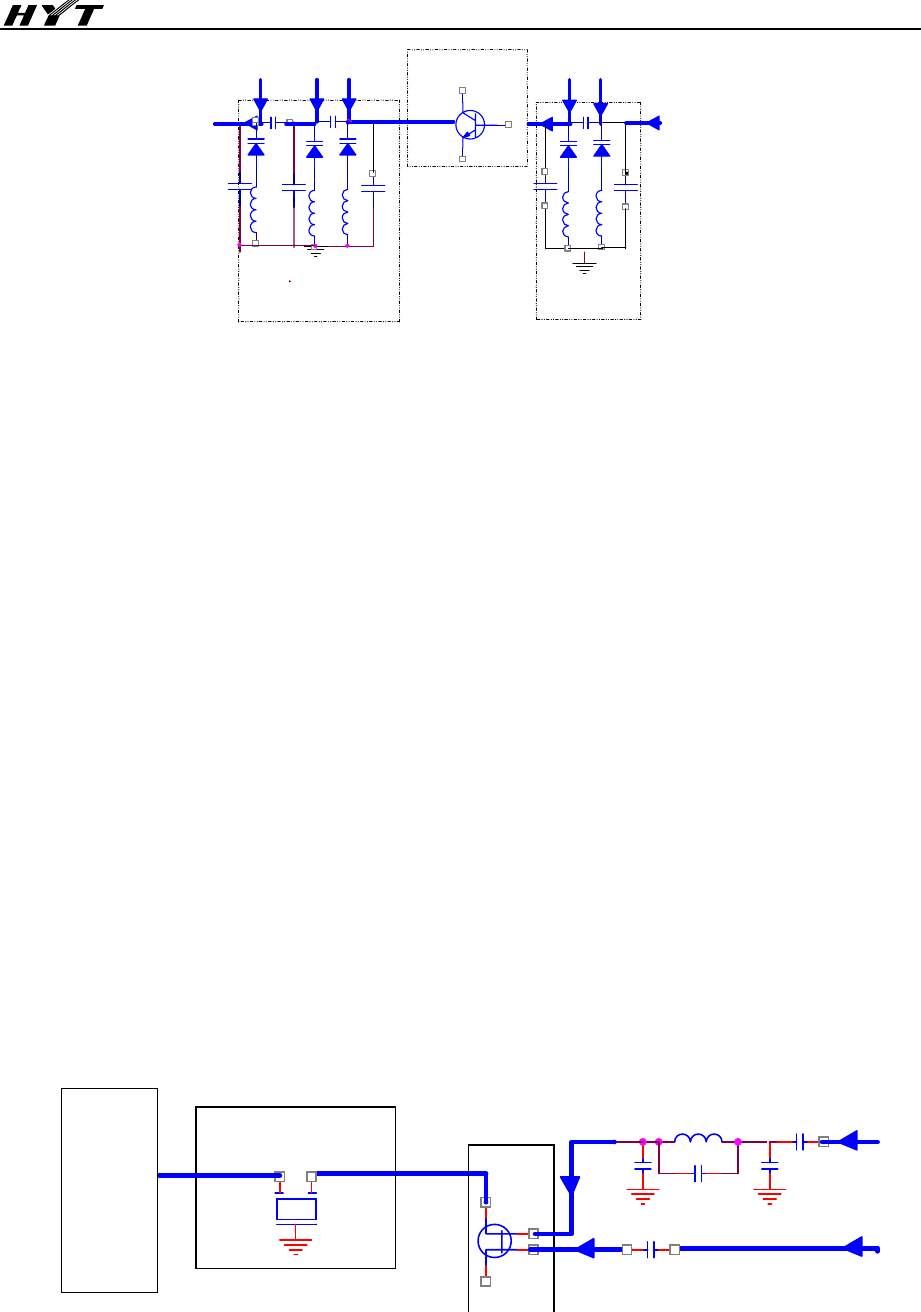
PLL Frequency Synthesizer
The PLL circuit generates local oscillator signals for reception and RF carrier signals for
transmission.
The PLL circuit consists of the VCO oscillator circuit and baseband processor chip and realizes
frequency tracking and channel conversion under the control of MCU signals.
1. PLL
MB95F108AK
WPFV-GE1
U605
1/2
17bitDIV
32/33
OSC
1/2
21bitDIV
U202
CP
RX-VCO
L102
D103
L101
APC/TUNE
T/R-SW
CLK
DATA
EN
Q101
2SK508NV
D102
BUFFER
Q6
1
23
D104
D101
D100
Q100
2SK508NV
12.8MHZ
TX-VCO
LPF
Q5
1
23
Figure 2
The step frequency of the PLL circuit is 5.0KHz, 6.25KHz, 10.0KHz or 12.5KHz. Therefore, the
reference oscillator signal (38.4MHz) is divided into 5.0KHz, 6.25KHz, 10.0KHz or 12.5KHz
reference signals by a fixed counter in PLL of U202. Signals output by VCO pass through buffer
Q102 followed by amplifier Q103 and enters PLL of U200 for frequency division by a variable
divider. The signals from the frequency division are compared with reference signals in the phase
comparator PD of PLL. Signals output by the phase comparator is added to the varactors D100,
D101, D102 and D103 of VCO to control the output frequency after passing through a low pass
filter.
2. VCO
The VCO section is realized by the oscillator circuit of three-point capacitor.
In transmitting mode, the operation frequency of VCO is generated by Q100; in receiving mode, the
operation frequency of VCO is generated by Q101.
10
U202 generates a control voltage via the phase comparator to control varactors (D100 and D101 in
transmitting mode; D102 and D103 in receiving mode) to bring the oscillator frequency of VCO in
line with the preset frequency of MCU within a broader frequency range.
The switching tube Q652 switches between transmitting and receiving under the control of T/R. In
transmitting mode, T/R is set as low level and Q100 operates when Q653 becomes conductive. In
receiving mode, T/R is set as high level and Q101 operates when Q653 cuts off. Output from Q100
and Q101 is sent to the buffer amplifier for process after passing through amplifier Q102.
If PLL is unlocked, LD pin of U202 outputs low level. When this situation is detected by a
microprocessor, transmitting and receiving operations are suspended and an alert tone sounds.
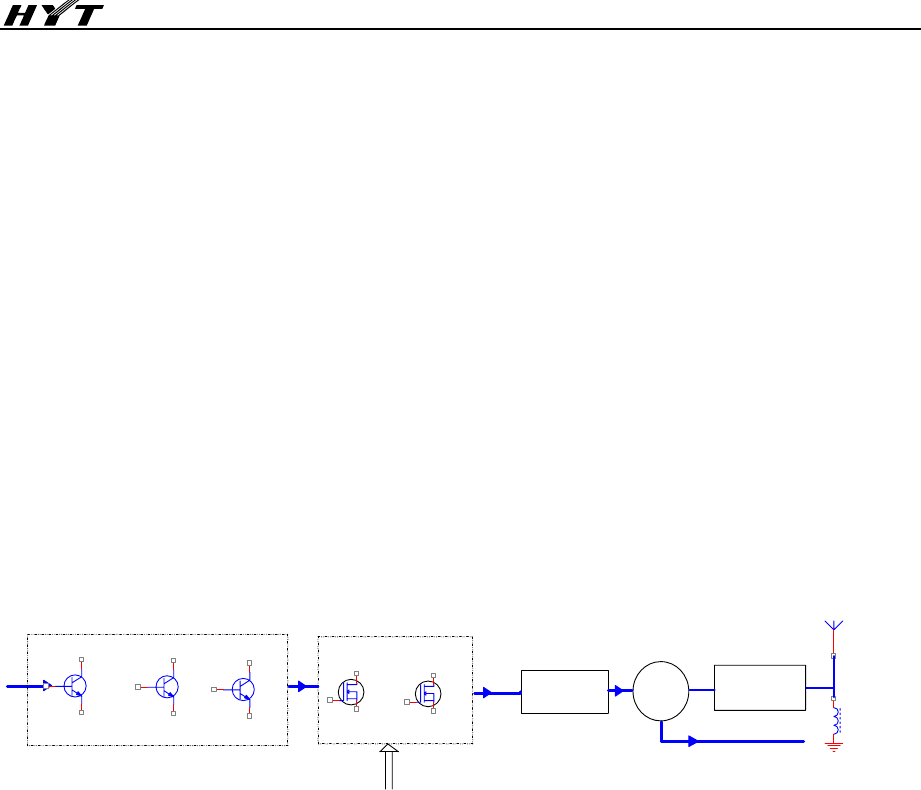
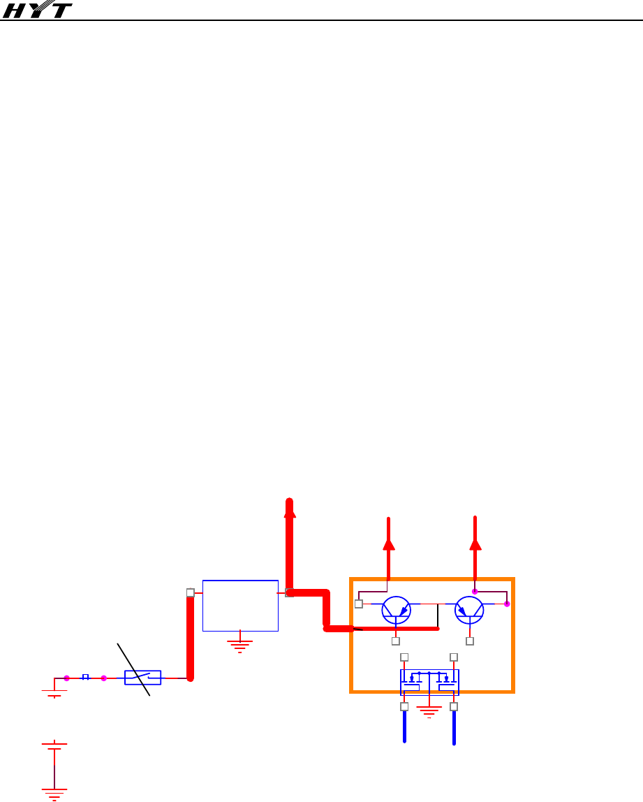
RF Power Amplifying Circuit (Tx Section)
Block Diagram for RF Power Amplifying Circuit
R/TSW
L453
1u
RX
RQA0002
2
13
3 Amplifier
Q401
2SC4988
1
23
APC
LPF
2SK3475
2
13
Q400
2SC5108
1
23
Q104
2SC5108
1
23
MATCH
ANTENNA
Q402
0
RF PA
Q403
Figure 3
To obtain the required RF power, RF signals from VCO is amplified by driving amplifiers Q400 and
Q401 after passing through buffer Q104. The amplified RF signals enters driver Q402, which
performs power pre-amplification on the input signals to derive a certain power to drive the final
power amplifier. The final power amplifier Q403 performs power amplification again on the input RF
signals to derive the required power. Then the amplified RF signals pass through Tx-Rx switching
diode D401 followed by the LC low pass filter circuit (LPF). The signals are transmitted through the
antenna after ultraharmonics are filtered by the LPF.
Rx Amplification (LNA) and RF Bandpass Network (BPF)
To obtain better frequency selectivity, the Rx bandpass utilizes multiple electrically tunable circuits.
The block diagram is shown below:
11
C505
LNA
TUNE BPF
TUNE FROM MCU
C504
C523
L508 L506
Q500
D503
L507
D506
1
23
L501
C526
C519
C524
L502
C521
C506
TUNE FROM MCU
D504
D505
D507
TUNE BPF
Figure 4
The Rx signals input from the antenna is filtered to remove out-of-band signals at the electrically
tunable bandpass network (D503, D504, L501, L502, C503, C505 and 507) and then amplified by
low-noise amplifier (LNA) Q500 to obtain a certain level required by reception. The signals pass
through the three-level bandpass network (mainly consisting of D505, D506, D507 and periphery
components) to effectively restrain the out-of-band interference and to derive pure Rx RF signals,
which will be fed to the mixing stage.
The electrically tunable control signals are provide by MCU. The required level can be obtained
through table looking up or formula computing to accurately control varactors to operate within
proper voltage range. It constitutes a bandpass filter with the periphery inductive capacitors to track
the Rx frequency under the change of MCU control voltage and to obtain the preset Rx sensitivity
requirements and out-of-band interference requirements.
Mixing Circuit (MIXER) and IF Bandpass Network (BPF)
Block Diagram for the Mixing Circuit
L53022nH
C533
C534 C532
C531
XF1
Q501
38.85MHZ
1stIF BPF
RF MIXER
AN29160
C528
Figure 5
The mixer mainly processes the local oscillator signals and Rx RF signals output by VCO. The first
IF from the mixer is used by the demodulator chip to discriminate frequency. Here the active mixer
12
is utilized.
The mixer tube (Q501) utilizes dual gate FET MOS (3SK318) and has better noise characteristics
and square law characteristics. The isolation between the local oscillator signals and the Rx signals
is high. To ensure proper sensitivity and certain gain for the mixer tube, tune delicately via the
offset.
The signals output from the mixer pass through inductor L509 to remove residual spurious and then
enter the first IF filter. The filter utilizes the first-class crystal filter to ensure sufficient bandwidth and
excellent selectivity. The signals finally enter baseband processing chip AN29160 for demodulation.
APC/TUNE Automatic Power Control Circuit
Block Diagram for the Circuit:
R430
R421 Q431
DTA114YE
R437
C441
R422
R441
R433
R434
from MCU
V_BAT
TX_VCC
R432
R440
C435
C437
R438
C436
R442
C438
-+
+-
U430
NJM2904
1
3
4
2
5
7
8
6
R436
Q430
DTC114EE
2
31
R431
R420
R439
R500
C440C439
to RF PA(APC)
C434
R435
to BPF(TUNE)
Figure 6
Subject to the selected channel, MCU outputs the corresponding PWM waveform, which is
reshaped by the RC filter network (R441, R442, C440 and C441) to derive the APC/TUNE control
signal level. One part of them is used as the control voltage of the electrically tunable circuit after
passing through R500. In transmitting mode, the levels are voltage-divided by R439 and R440 to
obtain the APC reference voltage.
The transmitting current passes through R420, R421 and R422 to derive the error detect voltage.
The voltage is amplified by operational amplifier IC U430 and then compared with APC reference
voltage to output APC control voltage and to form closed-loop negative feedback power control
when the transmitting current changes.
13
Audio and Signalling Processing Circuit
Baseband processing IC AN29160 has high integration level and powerful functions. Many of the
processing functions (as VCO level detect&output, SQ signal level detect&output, Tx-Rx audio
processing switch, audio amplifier, etc) and can be realized inside. The Tx-Rx sharing can also be
realized.
Block Diagram for Tx Audio&Signalling Process
D104
Q100
2SK508NV
TX-VCO
cpu
Pre
Emphasis
SF
AMP(TX)
sp Amp
Tone
AFMOD
Mic amp
U200
AN29160AA
PROCESSER
信令输入
AF
HPF
5th-HPF
mic
MIC
AF
mute
volume
mic mute
LIM
(TX)
0
Figure 7
Tx Audio Process: Audio signals input from the MIC is converted to electrical signals through the
audioelectric conversion of MIC and the amplitude limit of them are amplified by U200 after the
signals are pre-emphasized. The processed signals go to the low-pass filter circuit to remove
frequencies above 3KHz and then go to VCO for direct frequency modulation after passing through
potentiometer VR200.
Tx Sinalling Process: MCU outputs, via the QTO port, signalling encoder waveform, which is
divided into two parts for modulation after passing through the RC network. One part is used to
modulate PLL reference-frequency oscillator directly, while the other part is used to modulate VCO.
VR260 balances the modulation and adjust the signal amplitude ratio of one part to the other, which
optimizes the singalling waveform modulated on the carrier.
14
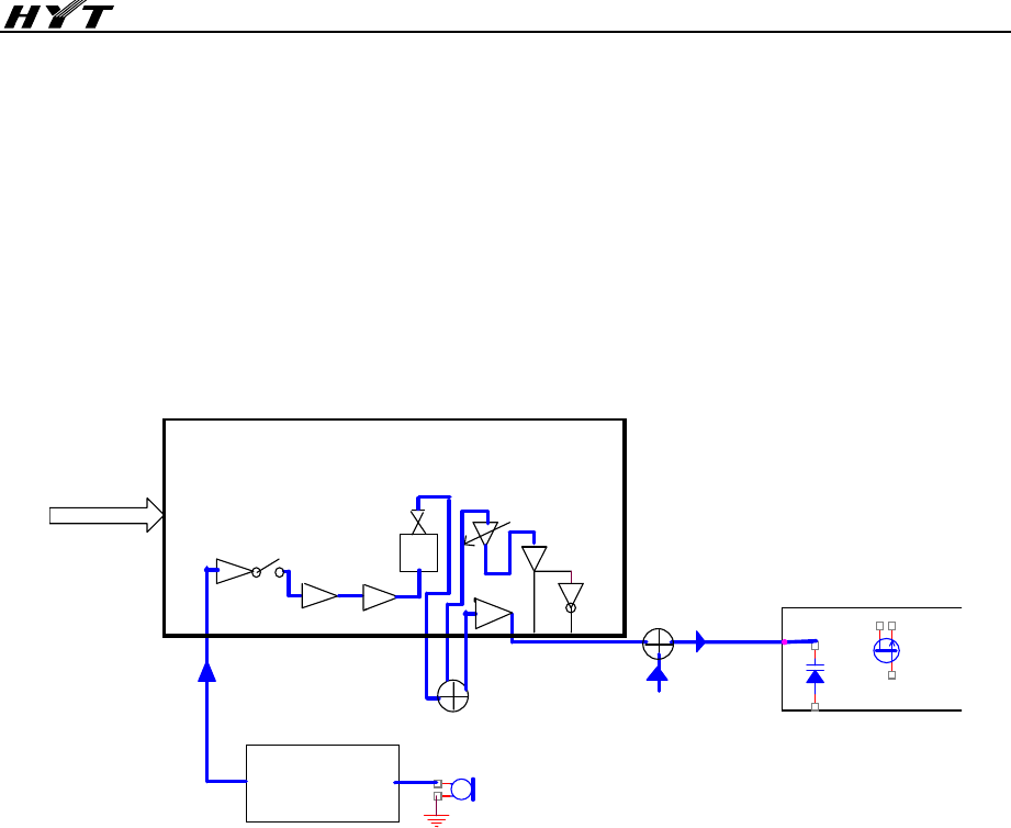
Block Diagram for Rx Audio&Signalling Process
RX
sp Amp
2ndIF BPF
SF
AMP(TX)
VOX
Tone
tone-LPF
DET
BGR
EN
RSSI
Mic amp
VCO
DATA
0
5th-LPF
IFAMP2
AF
HPF
PE
信令输出
5th-HPF
IFAmp1
SW
To MCU
IC
CF300
450KHz+/4.5K
OUT IN
VREF
TX
De
Emphasis
LATCH
AF
mute
SPVCC
volume
To MCU
CDC/CTC
MCU
mix2
mic mute
POWERREG
VCC
LIM
(TX)
SQ
AUDIO OUT
16Ω IW
U201
AF
AMP
U200
AN29160AA
PROCESSER
Figure 8
U200 outputs initial audio signals (including noise, signaling, audio, etc) after performing
frequency-discrimination and demodulation on the received signals. Therefore, the audio process
is divided into three parts:
Rx Audio Process: One part of the audio signal output by U200 is fed to the RC low-pass filter and
de-emphasis circuit and then amplified by U200. The audio signal is recovered after frequencies
below 300Hz are removed. The recovered audio signal is adjusted by the potentiometer and then
goes to audio power amplifier IC (U201), which amplifies power for the input audio signals to drive
the speaker directly. To obtain higher power, the BTL bridge dual output is utilized.
Rx Signalling Process: One part of the audio signal output by U200 is fed to the 300Hz low-pass
filter circuit (U640). After audio signals above 300Hz are removed, CTCSS/CDCSS goes to the
QTIN pin of CPU. CPU decodes the input signallings.
Noise Signalling Process: One part of the audio signal output by U200 goes to U200 again. After
the signal is filtered, amplified and rectified inside U200, a DC voltage signal (SQ) corresponding to
the noise component is derived. The DC signal is fed to the BUSY pin of MCU via the ND pin of
U200. Then MCU processes the input signals.
15
MCU Control Section
The block diagram for the MCU control section is shown below. MCU works under the 7.3728MHz
clock frequency.
Channel SW
MB95F108AK
WPFV-GE1
U605
PTT
MON
BAT
U609
APC/TUNE
PLL
1.vox
2.BUSY_DET
8.UART
7.W/N
6.DC/CTC
5.SAVE
4.T/R
3.BEEP/CALL
X601
9.BAT_DET
U610
Reset
IC
10.PLL_LD
7.3728M
晶体
Figure 9
The MCU control section is composed of MCU, EEPROM, RESET IC, keys, Channel Selector knob,
etc. Main functions realized by this circuit section are:
1. Control Signal:
Control of battery save mode
Control of high/low power switch
Control of band/narrow band switch
Control of Tx-Rx switch
Control of APC/TUNE output voltage
Control of Tx power supply and power supply of audio power amplifier
Control of squelch ON detect
2. Signal Detect
16
Detect of external PTT, MONI and VOX
Detect of PLL unlock (UL)
Detect of VOX ON level
Detect of battery power alarm
Detect of enabling and checking external remote speaker microphone
3. Data Transfer and Process
EEPROM data initiation
Programming data transfer
Encoding process of channel selector knob
Signalling encoding and decoding
Data transfer of baseband processing chip (PLL)
Power Supply Process
Block Diagram for the Circuit
SW
Q611
power management
Vin
VSS
Vout
---
7.2V
U606
L604
601s
SAVE
FMMT717FMMT717
Q612
5V
UPA572T
Q610
TXC
V-TX POWER-SAVE
Figure 10
After the radio is powered on, the battery voltage is provided to the RF power amplifier and audio
power amplifier to meet the requirements of sufficient power amplification after filtered by L604 and
C682. Another path is input with the regulator IC (U606) of 5V and outputs voltage of VCC_5V for
use by MCU and the baseband processing chip after regulated. Because the radio works under the
half duplex mode, it is required to control the Tx and Rx power supply alternately. To meet the
requirement of the battery save mode, MCU should output a pulse signal with fixed duty factor
17
(control signal of SAVE). When the SAVE signal of MCU is of high level, Q610 becomes conductive
and provides a 5V voltage (V_SAVE) for the operating circuit. PLL and the receiving circuit operate.
When the SAVE signal is a pulse signal, the radio enter the battery save mode. When transmitting,
TXC, control signal of CPU, is of high level. Q611 becomes conductive and provide a 5V voltage for
the transmitting circuit and the transmitting circuit operates.
Power supplies of the Tx section and Rx section both have symmetrical regulation measures.
When the load change changes the output voltage/current, the regulator closed-loop feedback
circuit operates, regulating the output voltage at 5V.
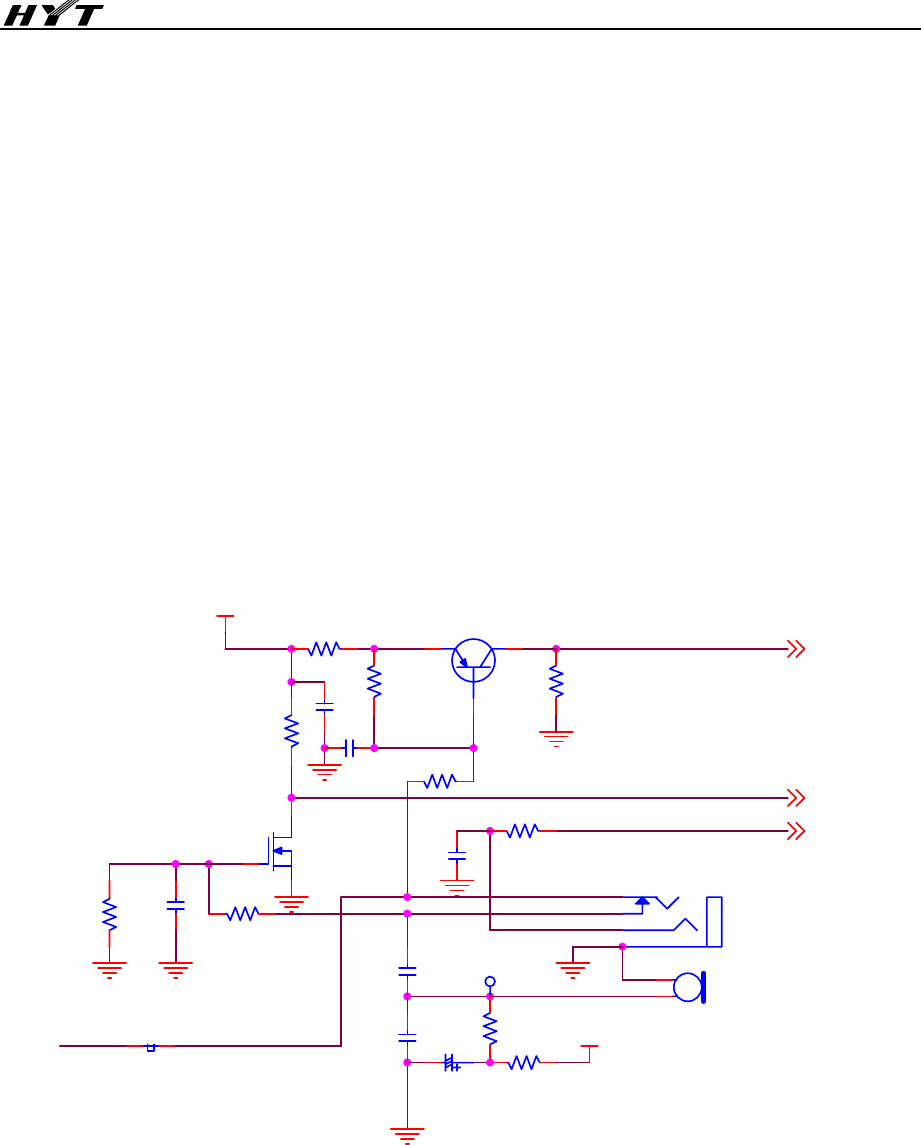
VOX Realization
The block diagram is shown below:
Q202
2SA1832
1
2 3
Q201
2SK1824
2
31
J4
MICJACK
2431
VCC_5V
R251
1M
MIC_EN
EXPTT
C260
220P
RXD
mic
X1
-
2
+
1
R201
2.2K
C201
470P
C200
4.7u/10V
R203
4.7K
VCC_5V
R200
470
C213
1U
C212
0.1U
R205
47K
C202
0.1U
L200 1UH
R202 100
TP200
R208
100K
R207
56K
R206 1K
R204 470
C274
0.01U
Figure 11
After the function key VOX is held down, the radio enters the VOX status. The VOX function can
only be enabled when MCU detect that MIC enabling signal (MIC_EN) and external VOX enabling
signal (EXT-PTT) switch from low level to high level almost at the same time (within hundreds of
milliseconds). Otherwise, it is detected as the earpiece without VOX and the VOX function is off.
18
When the remote speaker microphone with VOX is inserted into the earpiece jack, Q201 cuts off.
MIC_EN switches from low level to high level and Q202 completes the circuit with R204 and the
external remote speaker microphone simultaneously. Q202 becomes conductive. EXT-PTT
switches from low level to high level, which is detected by MCU as insert of a remote speaker
microphone with VOX. The VOX function is enabled. When the VOX detect level (5 levels available)
meets the preset requirements, the radio transmits and the audio signal goes to the baseband
processing IC AN29160 through the processing path.
If a remote speaker microphone without VOX (remote speaker microphone with PTT) is inserted,
Q201 cuts off. MIC_EN switches from low level to high level but Q202 can not complete the circuit
and keep the cut-off status. EXT-PTT is of low level. MCU detects as the remote speaker
microphone without VOX and the radio returns to the common mode. Press the PTT key on the
remote speaker microphone to transmit.
Semiconductor Data
Pin
No. Pin Name TC-610 TC-620 I/
ODescription
1 AVcc Vcc Vcc Power supply pin for A/D, connecting power
supply
2 AVR Vcc Vcc A/D reference input pin, connecting power
supply
3 PE3/INT13 PTT PTT I
PTT key (connected with pull-up resistor ) (valid
at low level)
4 PE2/INT12 A_KEY A_KEY I
SK1, programmable function key (connected
with pull-up resistor ) (valid at low level)
5 PE1/INT11 EXT-PTT EXT-PTT I
PTT key on the earpiece (connected with
pull-down resistor) (valid at high level)
6 PE0/INT10 B_KEY B_KEY I
SK2, programmable function key (connected
with pull-up resistor ) (valid at low level)
7 P83 ENC3 ENC3 I
8 P82 ENC2 ENC2 I
9 P81 ENC1 ENC1 I
10 P80 ENC0 ENC0 I
Encoder input of channel selector
knob(connected with pull-up resistor )
11 P71/TI0 T/R T/R O Tx-Rx switch control H(R)/L(T)
12 P70/TO0 Reserve Reserve O Reserved
13 MOD For down
-loading
For down
-loading I
An operating mode designation pin. When
downloading, this pin is connected with Vcc and
a resistor of 47K is also connected between the

19
pin and the grounded Vss. When not
downloading, only a resistor of 47K is connected
between the pin and the grounded Vss.
14 X0 OSC0 OSC0
15 X1 OSC1 OSC1
Connecting pin of 7.3728MHzMHz master
crystal oscillator
16 Vss GND GND Power supply (GND) pin (When recording, it is
connected with the GND recording port signals.)
17 Vcc VCC VCC MCU 5V power supply (When recording, it is
connected with the VCC recording port signals)
18 PG0 C C
This port can not be used as IO and a capacitor
is connected between the port and the grounded
Vss.
19 PG2/X1A OSC32K OSC32K
20 PG1/X0A OSC32K OSC32K Subsystem clock pin (Reserved)
21 /RST RESET RESET I
Reset (When recording, it is connected with the
RSTX recording port signals.)
22 P00/INT00 Reserve Reserve O
23 P01/INT01 Reserve Reserve O
24 P02/INT02 Reserve Reserve O
25 P03/INT03 Reserve Reserve O
Reserved
26 P04/INT04 PLLEN2 PLLEN2 I/
OPLL ENABLE
27 P05/INT05 PLLDATA
2
PLLDATA
2
I/
OPLL DATA
28 P06/INT06 PLLCLK2 PLLCLK2 I/
OPLL CLOCK
29 P07/INT07 UL2 UL2 I/
O
TB31202 PLL circuit unlock detect (H: Lock
L Unlock) (connected with pull-up resistor )
30 P10/UI0 RXD RXD I
UART RX (When recording, it is connected with
the UI recording port signals)
31 P11/UO0 TXD TXD O UART TX (When recording, it is connected with
the UO recording port signals)
32 P12/UCK0 Reserve Reserve O Reserved
33 P13/TRG0/A
DTG Reserve Reserve I Reserved
34 P14/PPG0 MIC_EN MIC_EN I
Check whether the MIC is connected(connected
with pull-down resistor) (valid at high level)
35 P20/PPG00 CTC_DCS CTC_DCS
P
W
M
CTCSS/CDCSS output
36 P21/PPG01 Reserve Reserve O Reserved
37 P22/TO00 TONE TONE O BEEP tone output/CALL tone output
38 P23/TO01 W/N W/N O Wide/Narrow band control W(L)/N(H)
39 P24/EC0 Reserve Reserve O Reserved

20
40 P50/SCL0 SCL SCL
S
C
L
EEPROM CLOCK
41 P51/SDA0 SDA SDA
S
D
A
EEPROM DATA
42 P52/PPG1 AP/TU AP/TU
P
W
M
Auto power control/adjust
43 P53/TRG1 TX_CTRL TX_CTRL O Tx power supply control “H”: valid
Transmission is on.
44 P60/PPG10 PLLCLK PLLCLK O PLL CLK
45 P61/PPG11 PLLDATA PLLDATA O PLL DATA
46 P62/TO10 PLLEN PLLEN O PLL ENABLE
47 P63/TO11 Reserve Reserve O Reserved
48 P64/EC1 Reserve Reserve O Reserved
49 P65/SCK Reserve Reserve O Reserved
50 P66/SOT Reserve Reserve O Reserved
51 P67/SIN Self Self I
For test (used to enter the factory clone mode,
connected with pull-up resistor)
52 P43/AN11 SPCNT SPCNT O Power supply control of main audio "H": audio O
N
53 P42/AN10 PCONT PCONT O Power supply control pin of AN29160AA
54 P41/AN09 RLED RLED O Red LED
55 P40/AN08 GLED GLED O Green LED
56 P37/AN07 Reserve Reserve O Reserved
57 P36/AN06 Reserve Reserve O Reserved
58 P35/AN05 TI TI
I/
A
D
CTCSS/CDCSS input
59 P34/AN04 BUSY BUSY
I/
A
D
Channel busy check (requiring 10-digit AD)
60 P33/AN03 BAT_DET BAT_DET
I/
A
D
Battery voltage detect (requiring 10-digit AD)
61 P32/AN02 Reserve Reserve O Reserved
62 P31/AN01 Reserve VOX
I/
A
D
VOX detect (requiring 10-digit AD)
63 P30/AN00 Reserve Reserve O Reserved
64 AVss GND GND Power supply (GND) pin for A/D, ground

21
Adjustment
User Mode
Power on the radio to enter the conventional mode when no key is pressed.
Programming Mode
In user mode, the PC programming software triggers the PC programming mode by communication
through a special communication protocol. The programming mode can set functions and
adjustment parameters of the radio via the PC programming software (including user version and
factory version).
Wired Clone Mode
Description
The wired clone mode is a separate mode. To enter other modes, the radio must be turned off and
back on.
The wired clone mode is classified into user wired clone mode and factory wired clone mode.
User Wired Clone Mode
Connect the two radios with the cloning cable. Power on the mother radio while holding down SK2
on it. The radio enters the wired clone mode in two seconds. Power on the slave radio directly and
the radio enters the user mode. The user wired clone mode clones the parameter data in EEPROM
of the mother radio into that of the slave radio. The transferred data only includes channel data and
shared setting parameters, excluding adjustment parameters, model version information, serial
number, etc.
Factory Wired Clone Mode
Short connect the SELF pin of the mother radio’s MCU and connect the two radios with the cloning
cable. Power on the mother radio while holding down SK2 on it. The radio enters the wired clone
mode in two seconds. Power on the slave radio directly and the radio enters the user mode. The
transferred data includes all data (excluding the serial number) in EEPROM and the switch icon of
the manual adjustment inhibit.
Process
Wired Clone
1. LED flashes orange once when the mother radio enters the wired clone mode. Press SK2 to

22
clone data into the slave radio.
2. During communication, LED of the mother radio flashes red, while LED of the slave radio
flashes green. When the communication is completed, red LED of the mother radio and green
LED of the slave radio go out, preparing for the next cloning.
3. During communication, if an exception occurs, the communication will be terminated. Red LED
of the mother radio goes out, preparing for the next cloning.
4. When the communication is completed, the mother radio returns to the preparing status. Press
SK2 to clone again.
Manual Adjustment Mode
Power on the radio while holding down PTT and SK2 simultaneously. The radio enters the manual
adjustment mode
Note: The operation is controlled by the switch of Manual Adjustment Inhibit in the programming
software. When the adjustment function is disabled, the radio can not enter the mode. This can
prevent users’ accidental entry and parameter changing, which will affect radio performances
During production, turn off the adjustment switch to avoid users’ accidental entry and from
changing adjustment values after the values are adjusted. The adjustment values can only be reset
in the production setting mode and are adjusted again according to the requirements. However,
they can not be changed in any other mode.
Adjustment Description
Enter Manual Adjustment Mode
Hold down PTT and SK2 simultaneously for two seconds at least to power on the radio. Orange
LED (red LED + green LED) lights, indicating the entry into the adjustment mode. Release the keys
to enter the N item (N is dependant on the location of the channel selector knob) of the Tx
adjustment items in the adjustment mode. The radio stays at the Tx adjustment items by default
and LED glows red.
Note: The CH15 adjustment item is invalid, while CH16 is used to toggle between Tx adjustment
items and Rx adjustment items. If the channel selector knob locates at CH15 or CH16, LED glows
neither red nor green.
Switch between Tx Adjustment Items and Rx Adjustment Items
Rotate the channel selector knob to CH16. Hold down PTT for 1.5s at least to toggle between Tx

23
adjustment items and Rx adjustment items. If LED lights red upon key pressing, the radio switches
to Tx adjustment items. If LED lights green upon key pressing, the radio switches to Rx adjustment
items.
LED glows red for Tx adjustment items.
LED glows green for Rx adjustment items.
Switch among Tx/Rx Adjustment Items
Switch via the channel selector knob.
Tx: CH1-CH14 indicate Tx preset power, Tx low power, Tx medium power, Tx high power, CDCSS
deviation, CTCSS deviation (low), CTCSS deviation (medium), CTCSS deviation (high), VOX 1,
VOX 2, VOX 3, VOX 4, VOX 5 and Tx low voltage threshold respectively.
Note: Tx medium power of TC-610/620 is not required to be adjusted. Please skip this item.
LED glows red for the adjustment items CH1-CH14.
CH15 is invalid and red LED goes out.
Rx: CH1-CH8 indicate SQL ON 1, SQL ON 5, SQL ON 9, SQL OFF 1, SQL OFF 5, SQL OFF 9, Rx
low voltage threshold and Rx bandpass filter respectively.
LED glows green for the adjustment items CH1-CH8.
CH9-CH15 are invalid and green LED goes out.
Wide/Narrow Band Switch in an Adjustment Item
In an adjustment item, hold down the PTT key for 1.5s at least. LED flashes orange, indicating the
long key pressing is valid. Release the key and the radio switches between wide band and narrow
band periodically. After the wide/narrow band switch, the adjustment point is regarded as the first
frequency of the current band by default.
Frequency Switch in a Band of an Adjustment Item
In a band of an adjustment item, short press the PTT key for less than 1.5s. LED flashes green,
indicating the short key pressing is valid. The radio switches frequencies one after another.
Plus-Minus of the Adjustment Value in a Band of an Adjustment Item
In a band of an adjustment item, short press SK1, and the adjustment value increases in step of 1.
Hold down SK1, and the adjustment value increases continuously in step of 1. When the
adjustment value gets to the maximum value allowed by the adjustment item, the adjustment value
will keep the maximum value constant.
In a band of an adjustment item, short press SK2, and the adjustment value decreases in step of 1.

24
Hold down SK1, and the adjustment value decreases continuously in step of 1. When the
adjustment value gets to the minimum value allowed by the adjustment item, the adjustment value
will keep the minimum value constant.
Process on Several Exceptional Items
Tx: CH9-CH14 indicate VOX 1, VOX 2, VOX 3, VOX 4, VOX 5 and Tx low voltage threshold
respectively, which are related with the AD sampling. After the above adjustment items are entered,
press SK1 or SK2 to start the AD sampling (including calculation process) once. Rotate the channel
selector knob to save the current AD sampling value. If SK1 or SK2 is not pressed, the AD sampling
is not started and the previous adjustment values can not be updated.
Rx: CH1-CH8 indicate SQL ON 1, SQL ON 5, SQL ON 9, SQL OFF 1, SQL OFF 5, SQL OFF 9 and
Rx low voltage threshold respectively, which are related with the AD sampling. After the above
adjustment items are entered, press SK1 or SK2 to start the AD sampling (including calculation
process) once. Rotate the channel selector knob to save the current AD sampling value. If SK1 or
SK2 is not pressed, the AD sampling is not started and the previous adjustment values can not be
updated.
Key Description
Short Press: key pressing time is less than 1.5s.
Long Press: key pressing time is 1.5s at least.
Description of Adjustment Items
25
Freq. 1 Freq. 2 Freq. 3 Freq. 4 Freq.5 Freq. 1 Freq. 2 Freq. 3 Freq. 4 Freq. 5
1Adjust preset RF power Y
2Tx low power YYYYY
3Reserved channel (not adjust)
4Tx high power YYYYY
5CDCSS deviation YYYYYYYYYY
6CTCSS (67Hz) deviationYYYYYYYYYY
7CTCSS (151.8Hz) deviatio
n
YYYYYYYYYY
8CTCSS (254.1Hz) deviatio
n
YYYYYYYYYY
9VOX gain1 Y
10 VOX gain2 Y
11 VOX gain3 Y
12 VOX gain4 Y
13 VOX gain5 Y
14 Tx low voltage threshold Y
1Carrier SQL level 1 ON YYYYYYYYYY
2Carrier SQL level 5 ON YYYYYYYYYY
3Carrier SQL level 9 ON YYYYYYYYYY
4Carrier SQL level 1 OFFYYYYYYYYYY
5Carrier SQL level 5 OFFYYYYYYYYYY
6Carrier SQL level 9 OFFYYYYYYYYYY
7Tx low voltage threshold Y
8Bandpass filter YYYYY
Note: Y indicates the valid adjustment frequency. The residual channels are idle and has no adjustment
items.
Tx Section
Rx Section
TC-610/620 Adjustment Items
Channel Adjustable Freq. Wide Narrow
Switch between Tx Adjustment Items and Rx Adjustment Items
Rotate the channel selector knob to CH16. Long press the PTT key for 1.5s at least to toggle
between Tx adjustment items and Rx adjustment items. If LED lights red upon key pressing, the
radio switches to Tx adjustment items. If LED lights green upon key pressing, the radio switches to
Rx adjustment items.
LED glows red for Tx adjustment items.
LED glows green for Rx adjustment items.
Wide/Narrow Band Switch and Frequency Switch in an Adjustment Item
In an adjustment item, long press the PTT key for 1.5s at least to switch between wide band and
narrow band periodically. The adjustment point is regarded as the first frequency of the current
band by default. Short press the PTT key for less than 1.5s to switch frequencies periodically.
Adjustment Items
Tx

26
Tx frequency tolerance, VCO lock voltage adjustment, maximum deviation and modulation
sensitivity
Note: These items are adjusted outside the adjustment mode (unnecessary to enter the adjustment
mode) via the hardware adjustment.
Tx low power, Tx high power, CDCSS waveform, CDCSS deviation, CTCSS deviation (low),
CTCSS deviation (high) and Tx low voltage threshold
Note: These items are adjusted inside the adjustment mode via the software adjustment.
Rx
VCO lock voltage adjustment (outside the mode), squelch, Rx bandpass filter, Rx low voltage
threshold
Specific Operations and Requirements
Conventional Adjustment Items (outside the adjustment mode): Tx frequency tolerance, VCO
voltage adjustment, maximum deviation, modulation sensitivity.
Note: The configuration file has preset CH1, CH2 and CH3 as wide band with low, medium and
high frequency respectively and CH4, CH5 and CH6 as narrow band with low, medium and high
frequency respectively. Make sure the antenna or load is connected before adjusting.
Measurement Adjustment
Adjustment Item Condition Test Equipment Test Point Part Method
Specifications/
Remarks
Tx frequency
tolerance
Rotate to
CH2. Press
PTT to
transmit.
Radio
communication
test set
Antenna VR300
Adjust VR300 with a
ceramic alignment
screwdriver to limit
the center frequency
to the error range.
≤150Hz
Rotate to
CH1. Press
PTT to
transmit.
Adjust TC100 with a
ceramic alignment
screwdriver until the
lock voltage is within
the required range.
0.7V (+0.1V)
Tx VCO
lock voltage Rotate to
CH3. Press
PTT to
transmit.
TC100
Check ≥2.3V
Rx VCO
lock voltage Rotate to
CH1.
Digital voltmeter CV
TC101 Adjust TC101 with a
ceramic alignment
screwdriver until the
0.7V (+0.1V)
27
lock voltage is within
the required range.
Rotate to
CH3. Check ≥2.3V
Wide
Rotate to
CH1, CH2
and CH3
respectively.
Press PTT
to transmit.
Adjust VR200 with a
ceramic alignment
screwdriver to limit
the deviation to the
specified range.
3.7-4.3KHz
Max.
Deviation
Narrow
Rotate to
CH4, CH5
and CH6
respectively.
Press PTT
to transmit.
Radio
communication
test set
LPF: 15kHz
AF:1kHz
150mV
VR200
Check 1.7-2.2KHz
Wide
Rotate to
CH1, CH2
and CH3
respectively.
Press PTT
to transmit.
Adjust the audio
output signal of the
radio communication
test set to get the
deviation to 3.0KHz.
10-20mV
Modulation
Sensitivity
Narrow
Rotate to
CH4, CH5
and CH6
respectively.
Press PTT
to transmit.
Radio
communication
test set
BPF: 0.3-3KHz
AF: 1KHz
Antenna
Earpiece
jack
Adjust the audio
output signal of the
radio communication
test set to get the
deviation to 1.5KHz.
10-20mV
Adjustments in the adjustment mode
Note: The antenna or load must be connected before adjusting.
Measurement Adjustment
Adjustment Item Condition Test Equipment Test
Point Parts Method
Specifications/
Remarks
Rotate to CH4.
Press PTT to
enable the
function.
Low frequency
Tx Power
High Short press
PTT to switch
frequencies
periodically
(refer to the
adjustment list)
Radio
communication test
set
Ammeter
Antenna
port
SK1
SK2 Press SK1/SK2 to
increase/decrease the
output power and
rotate the channel
selector knob to save.
4.5-5W
I≤1.7A

28
Rotate to CH2.
Press PTT to
enable the
function.
Low frequency
Low Short press
PTT to switch
frequencies
periodically
(refer to the
adjustment list)
Press SK1/SK2 to
increase/decrease the
output power and
rotate the channel
selector knob to save.
2W±0.3W
I≤1.2A
Rotate to CH5.
Press PTT to
enable the
function.
Low frequency
Adjust VR260 with a
ceramic alignment
screwdriver to
enable the
waveform
approximate to the
rectangular wave.
CDCSS Waveform Short press
PTT to switch
frequencies
periodically
and long press
PTT to switch
between wide
band and
narrow band.
VR260
Check
Rotate to CH5.
Press PTT to
enable the
function.
Wide band
Low frequency
Wide Press PTT to
switch other
frequencies
(medium-low,
medium,
medium-high
and high)
Adjust VR601 with a
ceramic alignment
screwdriver check
each frequency.
Adjust finely with SK1
and SK2 to limit the
CDCSS deviation to
the required range if
necessary.
500-800Hz
CDCSS
Deviation
Narrow Long press
PTT (≥1.5s) to
enter narrow
band.
Radio
communication test
set
LPF:0.3KHz
Antenna
VR601
SK1
SK2
Check 300-500Hz

29
Low frequency
Press PTT to
switch other
frequencies
(medium-low,
medium,
medium-high
and high)
Wide
Rotate to
CH6, CH7 and
CH8
respectively
and CTCSS is
set to low,
medium and
high. Press
PTT to enable
this function.
Wide band
Short press
PTT to switch
frequencies on
each channel.
Adjust VR601 with a
ceramic alignment
screwdriver and check
each frequency.
Adjust finely with SK1
and SK2 to limit the
CTCSS deviation to
the required range if
necessary.
500-800Hz
CTCSS
Deviation
Narrow
Long press
PTT (≥1.5s) to
enter narrow
band on CH6,
CH7 and CH8
and short press
PTT to switch
frequencies.
Radio
communication test
set
LPF:0.3KHz
Antenna
VR601
SK1
SK2
Check 300-500Hz
Low Tx Voltage
Threshold Digital voltmeter
Power
supply
port
Power
supply
Adjust the output
voltage of the power
supply and check the
alarm level
6.2V-7.0V(≤7.0V:
LED flashes;
≤6.2V: the alarm
tone sounds and
transmission
suspended)
Low voltage
Power-Off Level Digital voltmeter
Power
supply
port
Power
supply
Adjust the output
voltage of the power
supply and check the
power-off level
<5.80V

30
Item Condition Test Equipment Parts Method Specification/
Remarks
Rotate to CH8.
Low frequency
Rx Sensitivity
(bandpass)
Short press
PTT to switch
other
frequencies.
Radio
communication
test set
SSG:-119dB
MOD:1KHz
DEV:3.0KHz
Filter: 0.3-3KHz
Antenna
Remote
speaker MIC
jack
SK1
SK2
Check whether
SINAD is within the
range and whether to
get SINAD≥12dB by
adjusting SK1 or SK2.
Rotate the channel
selector knob to save
after the five-point
adjustment is
completed.
Adjust the
volume control
knob to the
right place,
which will not
limit the output.
SINAD≥12dB
Wide
Rotate to CH2
and SQL is set
to level 5 ON.
Press SK1 or
SK2 to enable
the function.
The channel
spacing is wide
band.
Low frequency
Short press
PTT to switch
frequencies.
Adjust the output
signals of SSG to the
squelch level. Rotate
the channel selector
knob to save after the
five-point adjustment
is completed.
SQL level:
-119±1dB
SQL
ON
Narrow
Long press
PTT (≥1.5s) to
enter narrow
band. Press
SK1 or SK2 to
enable this
function. Short
press PTT to
switch
frequencies.
Radio
communication
test set
SSG:-119dB
MOD:1KHz
DEV:1.5KHz
Filter: 0.3-3KHz
Antenna
Remote
speaker MIC
jack
SK1
SK2
Adjust the output
signals of SSG to the
squelch level. Rotate
the channel selector
knob to save after the
five-point adjustment
is completed.
SQL level:
-118±1dB

31
Wide
Rotate to CH5
and SQL is set
to level 5 OFF.
Press SK1 or
SK2 to enable
the function.
The channel
spacing is wide
band.
Low frequency
Short press
PTT to switch
frequencies.
Radio
communication
test set
SSG:-121dBm
Antenna
Remote
speaker MIC
jack
SK1
SK2
Adjust the output
signals of SSG to the
squelch level. Rotate
the channel selector
knob to save after the
five-point adjustment
is completed.
SQL level:
-121±1dB
SQL
OFF
Narrow
Long press
PTT (≥1.5s) to
enter narrow
band. Press
SK1 or SK2 to
enable this
function. Short
press PTT to
switch
frequencies.
Radio
communication
test set
SSG:-120dBm
Antenna
Remote
speaker MIC
jack
SK1
SK2
Adjust the output
signals of SSG to the
squelch level. Rotate
the channel selector
knob to save after the
five-point adjustment
is completed.
SQL level:
-120±1dB
Rx Low Voltage
Threshold
Adjust the output
voltage of the power
supply and check the
alarm level (LED
flashes red and the
alarm tone sounds)
≤6.50V
Low Voltage
Power-Off Level
Digital voltmeter Power supply
port
Power
supply
Adjust the output
voltage of the power
supply and check the
power-off level.
<5.80V

32
Appendix: Reference Voltage Setting of Battery Capacity
Check in transmitting mode
Green LED
(70%-100%)
>7.35V 18min
Orange LED
(50%-70%)
7.15V - 7.35V 12min
Red LED (30%-50%) 7.00V - 7.15V 12min
LED flashes red 6.20V - 7.00V 18min
LED flashes red
+an alarm tone
sounds every 10
5.80V - 6.20V
Halt <5.80V
Check in transmitting and standby mode (or press the battery capacity
check key.
Green LED
(70%-100%)
>7.55V 18min
Orange LED
(50%-70%)
7.35V-7.55V 12min
Red LED
(30%-50%)
7.00V-7.35V 20min
LED flashes red (<30%) 6.50V-7.00V 18min
LED flashes red
+an alarm tone sounds
every 10 seconds.
5.80V-6.50V
Halts <5.80V
33
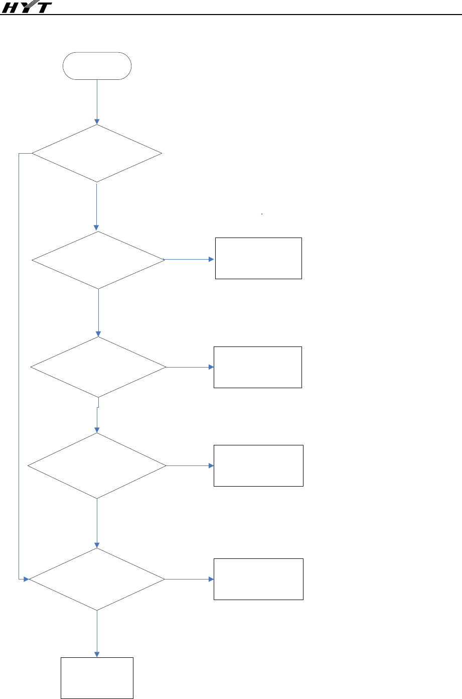
Troubleshooting Flow Chart
Tx Section
No
transmission
Start
Normal Tx
power supply?
D602 glows
red?
Check Tx
power supply
Tx VCO is
locked?
Check Tx
VCO
Check Tx
channel
Replace
D602
No voice during
transmission
Tx LED not
light
Check antenna
connection Check Q400, Q401,
Q402 and Q403
Yes
No
Check APC
control circuit
Low Tx
power
Check voice channel
(MIC, VR200 and
D104)
Replace
D602
Yes
No No
34
Rx Section
Start
No receive
Normal power
supply of receiving
circuit?
Yes
No
Check Rx power
supply circuit
Rx squelch level is
correct?
Normal Rx LED? Rx frequency is
correct?
Rx signalling is
correct?
Speaker works
well?
Normal audio
power amplifier?
Normal Volume
Selector knob?
P29 and P25, which are pins of
baseband processor ICU200,
output signals well?
Normal
demodulators?
Normal IF and
mixing circuits?
Normal RF mixing
circuit?
Change Rx
frequency
Change Rx
squelch level
Replace Rx
LED D601
Change Rx
signalling
Replace the
speaker
Check audio
power amplifier
circuit
Replace the
Volume
Selector knob
Check audio
processor
circuit
Check and
replace CD300
and CF300
Check Q105,
U200 (P12,P21)
and XF1
Check local
oscillator circuit
Q501
Check BPF
circuit Q500
Check antenna
connection
Yes
Yes
Yes
Yes
Yes
Yes
Yes
Yes
Yes
No
No
No
No
Completed
Yes
Yes
No
No
No
No
No
No
No
35
MCU
Start
Normal power-on alert
tone?
Speaker works well?
Yes
No
Yes
No
MCU clock crystal X601
works well?
MCU operating voltage
VCC works well?
Yes
No Check U606
Replace X601
No
Yes
Check whether other
control pins control well.
MCU works
well
Yes
No
Check pin
connection or
recording
programme
Replace the
speaker
36
Disassembly and Assembly
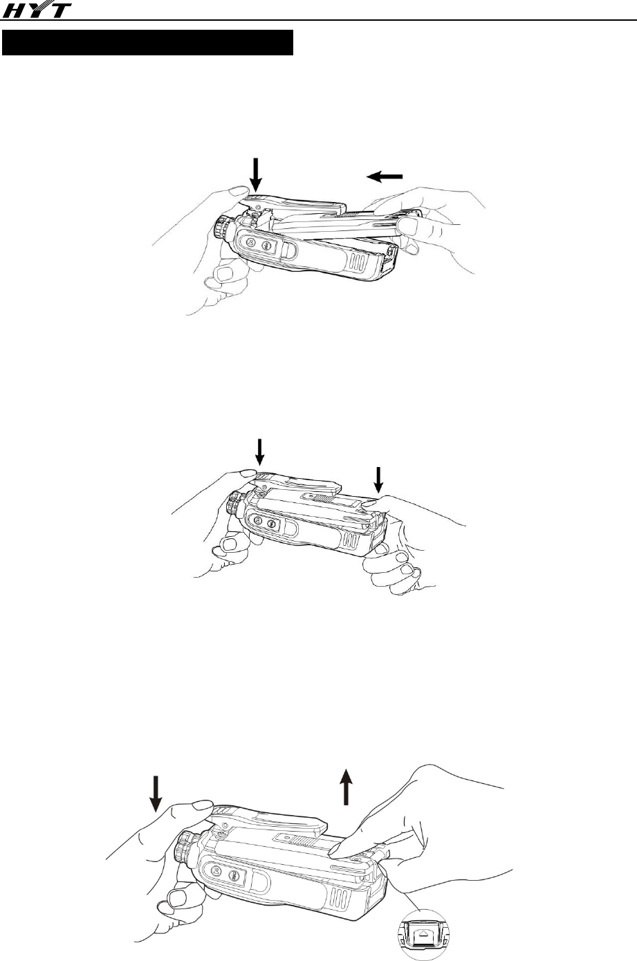
Attaching the Battery
① Hold the battery and push it towards the top of the aluminum chassis under the belt clip of the
radio. See figure 1.
Note: Insert the tabs at the top of the battery into the top of the battery slots.
Figure 1
② Press the bottom of the battery until a “click” is heard to fasten the battery on the bottom of the
radio. See figure 2.
Note: If the battery is not fastened or is still adrift, please remove the battery and attach it again.
Figure 2
Removing the Battery
①Turn off the radio. Hold the upper side of the radio and press the belt clip until it tilts. Push the
battery latch upwards along the slot of the battery latch at the bottom of the battery. See figure 1.
Figure 1
37
② Release the battery latch and remove the battery when the bottom of the battery tilts. See figure
2.
Note: To avoid serious abrasion between the tab on the top of the battery and the slot on the top of
the radio, the angel between the radio unit and the tilting battery must not be too large.
Figure 2
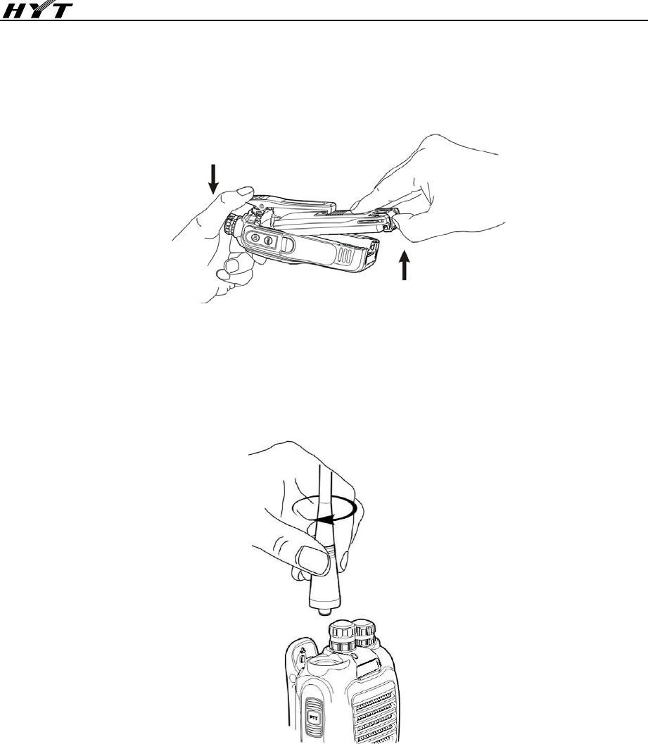
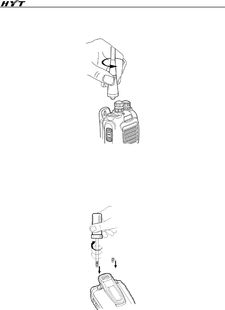
Attaching the Antenna
① Insert the threaded end of the antenna into the big threaded hole at the top of the radio.
② Rotate the antenna clockwise until it is fastened.
38
Removing the Antenna
Rotate the antenna counter-clockwise to remove the antenna.
Attaching the Belt Clip
Loose the screw for the belt clip and fix the belt clip on the radio unit. Align the hole on the belt clip
with that on the aluminum chassis and rotate the screw for the belt clip clockwise to fasten the clip.
See figure 1.
Figure 1
Removing the Belt Clip
Please refer to the steps for attaching the belt clip when removing the belt clip. Loose the screw by
rotating it counter-clockwise. See figure 2.
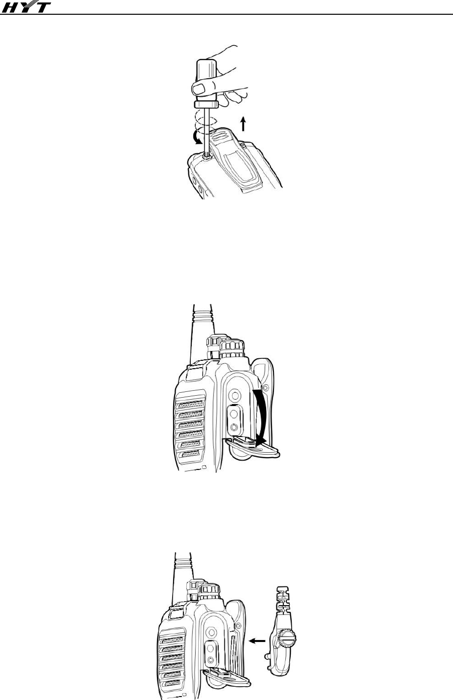
39
Figure 2
Attaching the External Earphone/Microphone
① Open the earphone/microphone jack cover (unnecessary to remove). See figure 1.
Figure 1
② Plug the earphone/microphone into the jack and fasten the screw. See figure 2.
Figure 2

40
Removing the External Earphone/Microphone
Loose the screw and unplug the earphone/microphone.
Note: When the external earphone/microphone is used, the radio’s waterproof performance will be
affected.
41
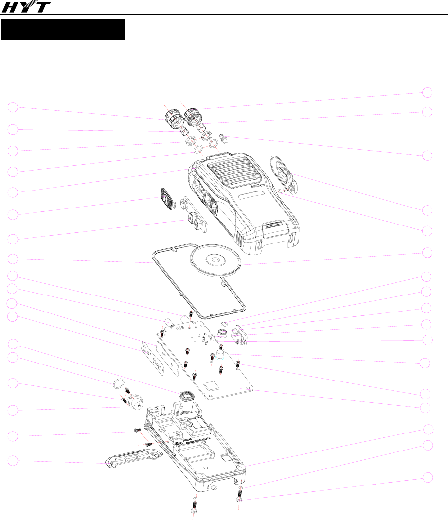
Exploded View
TC-610
8
9
10
11
12
13
14
15
16
1
3
2
7
6
5
4
17
18
19
20
21
22
23
24
25
26
27
28
29
30
31
32
33
34
35
42
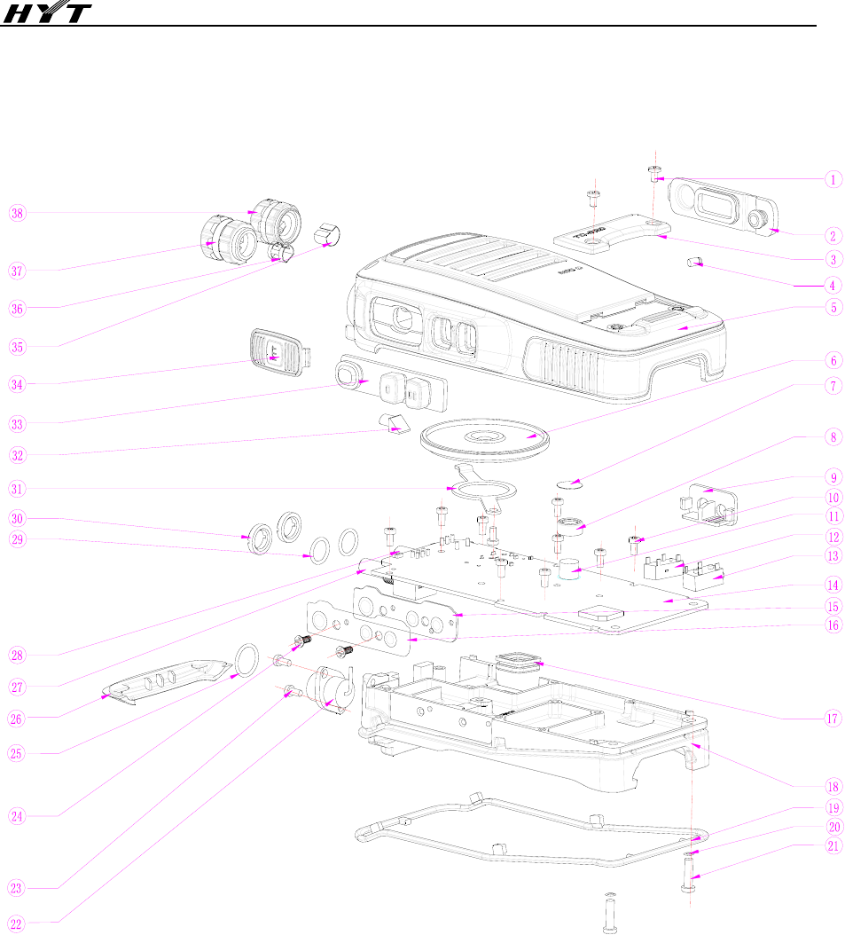
TC-620

43
TC-610/620 Parts List 2
TC-610
No. Material No. Description Qty.
1 6000631000000 Volume control knob 1
2 6201006000000 Inner liner knob 1
3 7207002200200 Nut 2
4 6100325000000 O-RING (knob) 2
5 1500006100000 Front case kit 1
6 6000634000000 Plastic PTT key 1
7 6100312000000 Silica rubber PTT key 1
8 6100307000000 Waterproof ring (main unit) 1
9 4303020000020 Volume control knob 1
10 4304030000010 Gray-code range switch 1
11 6100314000000 Waterproof ring (battery connector) 1
12 6100246000000 O_RING (antenna) 1
13 7102504000300 Machine screw 2
14 4400100008000 SMA-connector 1
15 4100510300000 PCB (PTT key) 1
16 7300029000000 Metal dome (3-key)
17 7102005000000 Machine screw 2
18 6000627000000 Rear cover (radio unit) 1
19 7102508000000 Machine screw 2
20 7400216000000 TC-610 waterproof PC sheet 2
21 6300051000000 Aluminum chassis 1
22 4100610100000 PCB (main board) 1
23 7102004020100 Self-tapping screw 9
24 5002220000050 MIC 1
25 5205000000190 Earpiece jack 1
26 5205000000280 Speaker jack 1
27 6100123000000 MIC cover 1
28 6100323000000 Holder (speaker jack) 1
29 7400184000000 Waterproof mic net 2
30 5001210000030 Speaker 1
31 6000127000000 Earpiece cover stopper 1
32 6000635000000 Earpiece cover 1
33 6000640000000 Light guide 1
34 6201066000000 Inner liner knob 1
35 6000630000000 Channel selector knob 1

44
TC-620
No. Material No. Description Qty.
1 7102003500100 Machine screw 2
2 6000639000000 Earpiece cover 1
3 6300040000000 Decorative plate (zinc alloy) 1
4 6000127000000 Earpiece cover stopper 1
5 1500006200000 Front case kit 1
6 5001210000170 Speaker 1
7 7400141000000 NSM08Z01mic net 2
8 6100123000000 MIC cover 1
9 6100323000000 Holder (speaker jack) 1
10 7102004021030 Self-tapping screw ST2.0*3.8mm 10
11 5002220000050 MIC 1
12 5205000000280 Speaker jack 1
13 5205000000190 Earpiece jack 1
14 4100610100000 PCB (main board) 1
15 4100510300000 PCB (PTT key) 1
16 7300029000000 Metal dome (PTT key) (3-key) 1
17 6100314000000 Waterproof ring (battery connector) 1
18 6300051000000 Aluminum chassis 1
19 6100307000000 Waterproof ring (radio unit) 1
20 7400216000000 Waterproof transparent PC sheet 2
21 7102508000000 Machine screw M2.5*8.0mm 2
22 4400100008000 SMA-connector 1
23 7102504000300 Machine screw M2.5*4.0mm 2
24 7102005000000 Machine screw M2.0*5.0mm 2
25 6100246000000 O_RING (antenna) 1
26 6000629000000 Rear cover (radio unit) 1
27 4303020000020 Volume control knob 1
28 4304030000010 Gray-code range switch 1
29 6100325000000 O-RING (channel selector knob) 2
30 7207002200200 Nut M7.0*2.2mm 2
31 6201545000000 Speaker tablet 1
32 6000624000000 Light guide 1
33 6100312000000 Silica rubber PTT key 1
34 6000634000000 Plastic PTT key 1
35 6201006000000 Inner liner knob 1
36 6201066000000 Inner liner knob 1
37 6000631000000 Volume control knob 1
38 6000630000000 Channel selector knob 1
45
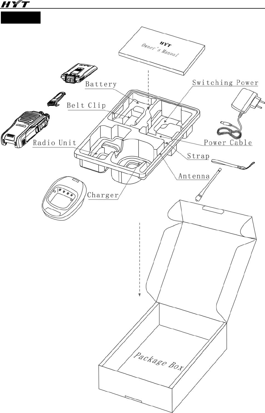
Packing

46
TC-610/620 PCB View

47
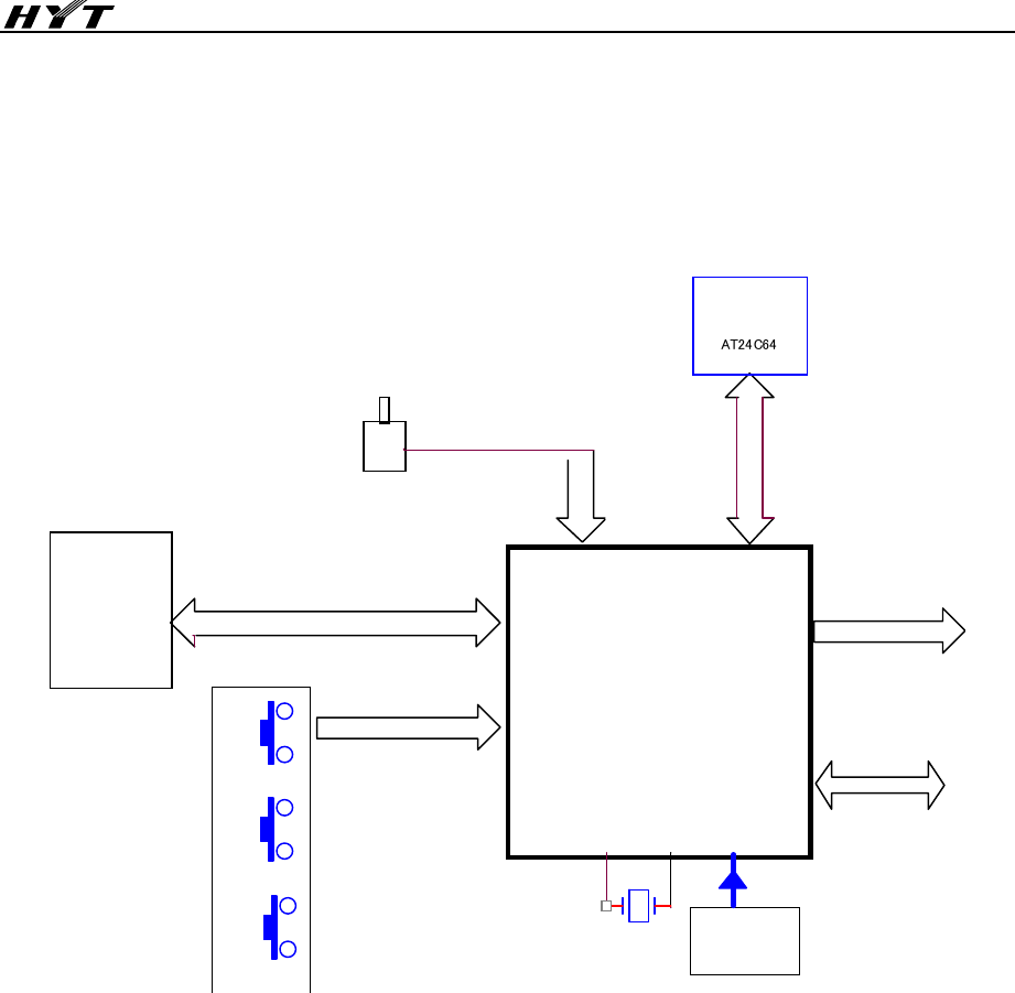
TC-610/620 Block Diagram
1
TC-610/620 Level Diagram
Q101
2SK508NV
1W(BTL)200mVrms-120dBm -103dBm -67dBm
-69dBm
250mVrms-98dBm-108dBm-104dBm-122dBm
LPF
IFAmp 1 AF HPF Volume
MIX2
2ndIF
BPF
IFAmp 2
DET
de-emphasis
23 25 29 44
AF mute
AN29160
5221
16mVrms
-10dBm
Q102
1
23
D104
37dBm39dBm
Q400 2SC5108
1
23
27dBm
LPF
2SK3475
Q402
2
13
15dBm-8dBm450mVrms
stimulator power AMP
Mic Amp
Mic Mute
AF HPF LMT SF Amp
AN29160
5140
MICROPHONE
47K
VR200
C112
AF AMP
TDA2822
150mVrms -26dBm
D400
D500
SW
Q401 2SK4988
1
23
-45dBm
Q104
1
23
16Ω IW
Q500
AT41511
RQA0002
Q403
2
13
attenuator
step1to23
buffer
Q501
3SK318
3
2
41
Q100
2SK508NV
BPF BPF
38.85M
C
3dBm
C130 C141
VCO
C400
C405
C402 C429
C412
TUNE BPF 1stIF BPFRF MIXERTUNE BPF LNA
TX PART
RX PART
RFAF
RF AFIF
1
TC-610/620 Schematic Diagram
Specifications
General
Frequency Range
146-174 MHz
400-420 MHz
450-470 MHz
Channel Capacity 16
Channel Spacing 25/12.5 MHz
Operating Voltage 7.5V DC
Battery Life (5-5-90 Duty
Cycle) About 8 hours
Operating Temperature -20~+50℃
Dimensions (H×W×D) TC-610:119mm x 54.6mm x 32.5mm (without antenna)
TC-620:117mm x 54.3mm x 31mm (without antenna)
Weight TC-610: 270g (with antenna)
TC-620: 275g (with antenna)
Frequency Stability ±2.5ppm
Receiver
Sensitivity -119dBm/-118dBm
Adjacent Channel Selectivity ≥65(W)/55(N)
Intermodulation ≥60dB
Spurious Response Rejection ≥65dB
Audio Power Output 1200mW
Transmitter
RF Power Output 5±0.5W(H)/2.0±0.3W(L)
Spurious and Harmonics <1GHz: -36dBm/>1GHz: -30dBm
Modulation Limitation 5 KHz/2.5KHz
FM Noise 40dB(W)/35dB(N)
Modulation Distortion ≤5%
All Specifications are tested according to TIA/EIA-603, and subject to change without notice due to continuous
development.

2
HYT endeavors to achieve the accuracy and completeness of this manual, but no warranty of
accuracy or reliability is given. All the specifications and design are subject to change without prior
notice due to continuous technology development. Changes which may occur after publication are
highlighted by Revision History contained in Service Manual.
No part of this manual may be copied, reproduced, translated, stored in a retrieval system,
distributed, or transmitted in any form or by any means, electronic or mechanical, for any purpose
without the express written permission of HYT.