HYT Science and Technology Co TC-700U8 Two-way Radio User Manual TC 700 Service Manual 01
Shenzhen HYT Science &Technology; Co Ltd Two-way Radio TC 700 Service Manual 01
Users Manual
Contents
General……………………………………………………………………………
Brief Introduction………………………………………………………………
Software Specification………………………………………………………….
Circuit Description……………………………………………………………
CPU Pins…………………………………………………………………………
Part List 1………………………………………………………………………
Adjustment Description……………………………………………………….
Trouble-shooting Chart……………………………………………………….
Disassembly and Assembly for Repair……………………………………
Exploded View…………………………………………………………………..
Part List 2………………………………………………………………………...
Packing…………………………………………………………………………..
PC Board View…………………………………………………………………
Level Diagram…………………………………………………………………
Schematic Diagram…………………………………………………………….
Description of TC-700 Desktop Charger……………………………………
Specifications…………………………………………………………………...

TC-700 General
1
Revision History
Edition Release Date Revised Content
8130070000000 2005/09/22 Initial release
2006/09/22
1) 2-Tone/5-Tone, add HDC1200 and HDC2400TM
2) Update schematic diagram and part list
3) Update exploded view, part list and diagram for
disassembly and assembly
General
Manual Scope
This manual is intended for use by experienced technicians familiar with similar types of
communication equipment. It contains all service information required for the equipment and is current
as of the publication date.
User Safety Information
The following precautions are recommended for personnel safety:
z DO NOT transmit until all RF connectors are verified secure and any open connectors are
properly terminated.
z SHUT OFF and do not operate this equipment near electrical blasting caps or in an explosive
atmosphere.
z When in vehicles with an airbag, do not place a portable radio in the area over an airbag or in the
airbag deployment area.
z Do not expose the radio to direct sunlight for a long time nor place it close to a heating source.
z Do not use any portable radio with a damaged antenna. If a damaged antenna comes into contact
with your skin, a minor burn may result.
z When transmitting with a portable radio, hold the radio in a vertical position with its microphone
about 5 centimeters away from your mouth.
z If you wear a portable radio on your body, be sure to keep the antenna at least 2.5 centimeters
away from your head or body when transmitting.
z This equipment should be serviced by a qualified technician only.
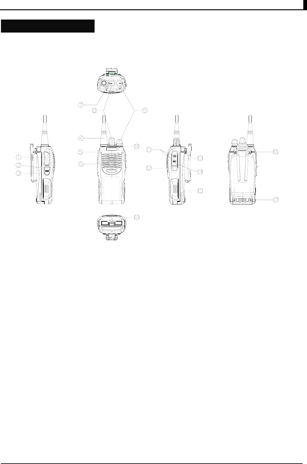
TC-700 Brief Introduction
2
Brief Introduction
Control Knob and Function Key
(1) PTT Key(Push-To-Talk Key)
Select transmit/receive mode. Press and hold PTT, radio operates in transmit mode. Release
PTT, radio returns to receive mode.
(2) SK1 Key
Side Key1, programmable key
(3) SK2 Key
Side Key2, programmable key
(4) Antenna
(5) Microphone
(6) Speaker
(7) TK Key
Top Key, programmable
(8) Channel Selector Knob
Rotate the knob to select Channel1 to 16

TC-700 Brief Introduction
3
(9) Power/Volume Control Knob
Rotate the Power/Volume Control Knob clockwise to turn the radio on; fully counter clockwise
to turn the radio off. Increase or decrease volume by adjusting the volume control accordingly.
(10) LED Indicator
Red LED glows while transmitting; green LED glows while receiving; red LED flashes when
the battery voltage is low.
(11) External Jack
(12) Earplug Cover Screw
(13) Earplug Cover
(14) Belt Clip
(15) Battery
(16) Belt Clip Screw
(17) Charging Connector
(18) Release Button

TC-700 Software Specification
4
Software Specification
Specification:
Conventional Mode
1. Mechanical Knob (16 channels)
VHF:136~174MHz
UHF:400-470MHz, 450~520MHz
2. Channel Spacing: 25/20/12.5KHz (Wide/Medium/Narrow bandwidth compatible)
3. Step: 2.5/5/6.25KHz
4. LED Indicator: Red/Green
5. 3 Programmable Function Keys
6. CTCSS/CDCSS Encode & Decode
7. DTMF Encode
8. 2-Tone (2-Tone version) / 5-Tone (5-Tone version)
9. HDC2400TM Encode & Decode
10. HDC1200 Encode & Decode
11. Squelch Mode:
1) Carrier
2) CDCSS/CTCSS
3) Optional Signalling
4) CTCSS/CDCSS AND 2-Tone/5-Tone/ HDC2400TM/HDC1200
5) CTCSS/CDCSS OR 2-Tone/5-Tone/ HDC2400TM/HDC1200
12. Scan
13. Time-Out-Timer (TOT)
14. Rent
15. Battery Save
16. Emergency
17. PTT ID
18. Busy Channel Lockout & Busy Tone Lockout
Description
1. User Mode
This mode is for normal operation.
2. All Reset Mode
Firstly ground the SELF point, and then turn the power on while holding down TK key for 2 seconds.
The radio enters all reset mode with green LED flashing twice. Turn the channel selector knob to the

TC-700 Software Specification
5
selected channel and press PTT, the radio data is all reset (All clone modes will be automatically
activated when All Reset is completed). Frequency settings are shown as follows:
Channel data is shown as follows:
Channel RX Frequency
(MHZ)
TX Frequency
(MHZ) Signaling Power Channel
Spacing
1 RX1 TX1 None H 25KHZ
2 RX3 TX3 None H 25KHZ
3 RX5 TX5 None H 25KHZ
4 RX1 RX1 None LO 20KHZ
5 RX3 RX3 None LO 20KHZ
6 RX5 RX5 None LO 20KHZ
7 RX1 RX1 None LO 12.5KHZ
8 RX3 RX3 None LO 12.5KHZ
9 RX5 RX5 None LO 12.5KHZ
10 RX3 RX3 67HZ LO 25KHZ
11 RX3 RX3 254.1HZ LO 25KHZ
12 RX3 RX3 023 LO 25KHZ
13 RX3 RX3 754 LO 25KHZ
14 RX3 RX3 2-TONE LO 25KHZ
15 RX3 RX3 5-TONE LO 25KHZ
16 RX3 RX3 None LO 25KHZ

TC-700 Software Specification
6
3. Wireless Clone Mode
Select wireless clone from optional functions in programming software, turn the power on while
holding down PTT and SK1 key simultaneously for 2 seconds, then the source and target radios
enter wireless clone mode with orange LED flashing one time(After the source and target radios are
turned on and stay in the same channel, hold down PTT on the source radio to begin cloning).
During cloning, the LED of the source radio glows red and that of the target radio glows green. The
target radio flashes green and two Beeps are heard in case of successful cloning, it flashes red in
case of cloning failure.
4. User Wired Clone Mode
Select Wired Clone from optional functions in programming software, turn the power on while
holding down PTT and SK2 key simultaneously for 2 seconds, then the source radio enters user
wired clone mode with orange LED flashing twice. Then directly turn the target radio on. Hold down
PTT on the source radio to begin cloning. During cloning, the LED of the source radio glows red and
that of the target radio glows green. The LED of the source radio goes out in case of successful
cloning, it flashes red in case of cloning failure.
5. Manual Adjust Mode
Manual adjustment is performed to adjust frequency deviation, power, sensitivity, squelch, etc.
Note: Prior to entry for mode startup, select Manual Adjust Mode from optional functions in
programming software.
Manual Adjust Mode Description
(1) Enter the manual adjust mode
Turn the power on by holding down TK and SK2 key simultaneously for 2 seconds, then the radio
enters manual adjust mode with red LED flashing twice.
(2) Channel number on the channel selector knob
Each channel on the channel selector knob is defined as a setting item. 25KHz bandwidth and low
frequency (F1) is set on the next channel each time the Channel Selector Knob is rotated.
(3) SK2 key
Used to set the frequency. 1 point tuning adjusts center frequency; 3 point tuning adjusts F1, F3,
F5; 5 point tuning adjusts F1-F5.
The frequency toggles from low frequency to high frequency. Green LED flashes once when F1 is
selected.

TC-700 Software Specification
7
(4) TK key
Use to toggle the channel bandwidth among 25 KHz, 20 KHz and 12.5 KHz. Red LED flashes
once when the bandwidth is 25 KHz.
(5) PTT/SK1
PTT→Increase
SK1→Decrease
PTT/SK1 is pressed to adjust upward/downward. Red LED glows indicating the maximum adjust
value and green LED indicating the minimum value. Hold down the key to increase/decrease the
adjustment value continuously.
Press PTT key to save the BATT LOW, and SQL settings, then green LED glows once.
(6) Select adjustment item group
The first group of adjustment items is selected when the radio enters the manual adjust mode.
Turn to CH16 and press PTT key to enter the next group. Press it again to return to the first group.
Orange LED flashes once when the first group of adjustment items is selected and flashes twice
when the second group is selected.
(7) Frequency Setting
5 point tuning(MHz) TX: { TX1,TX2,TX3,TX4,TX5}
RX: {
RX1,RX2,RX3,RX4,RX5}
3 point tuning(MHz) TX: { TX1, TX3, TX5}
RX: {
RX1, RX3, RX5}
1 point tuning(MHz) TX: { TX3}
RX: {
RX3}

TC-700 Software Specification
8
First Group of Adjustment Items
Channel No. Adjustment Item Remarks
25KHz 20KHz 12.5KHz
1 TX power LOW 5 point tuning
2 CDCSS PLL balance 3 point tuning (wideband)
3 CDCSS deviation 3 point tuning (wideband) 1 point tuning 1 point tuning
(narrowband)
4 CTCSS deviation LOW (67Hz)
3 point tuning (wideband) 1 point tuning 1 point tuning
(narrowband)
5
CTCSS deviation CENTER
(136.5Hz)
3 point tuning (wideband) 1 point tuning
1 point tuning
(narrowband)
6 CTCSS deviation HIGH (254.1Hz) 3 point tuning (wideband) 1 point tuning 1 point tuning
(narrowband)
7 AK2346 audio deviation (TX) 3 point tuning (wideband) 1 point tuning 1 point tuning
(narrowband)
8 2 TONE deviation 1 point tuning (wideband) 1 point tuning 1 point tuning
(narrowband)
9 DTMF deviation 1 point tuning (wideband) 1 point tuning 1 point tuning
(narrowband)
10 MSK deviation 3 point tuning (wideband) 1 point tuning 1 point tuning
(narrowband)
11 TX power HIGH 5 point tuning
12 TX voltage LOW 1 point tuning

TC-700 Software Specification
9
6. PC Adjust Mode
Select test mode from programming items in programming software and then begin adjustment.
Second Group of Adjustment Items
Channel No. Adjustment Item Remarks
25KHz 20KHz 12.5KHz
1 RX sensitivity 5 point tuning
2 AK2346 volume (RX) 1 point tuning (wideband) 1 point tuning 1 point tuning
(narrowband)
3 Squelch level 3 (OPEN) 5 point tuning (wideband) 1 point tuning 1 point tuning
(narrowband)
4 Squelch level 3 (SQUELCH) 5 point tuning (wideband) 1 point tuning 1 point tuning
(narrowband)
5 Squelch level 9 (OPEN) 5 point tuning (wideband) 1 point tuning 1 point tuning
(narrowband)
6 Squelch level 9 (SQUELCH) 5 point tuning (wideband) 1 point tuning 1 point tuning
(narrowband)
7 RX voltage LOW 1 point tuning
TC-700 Circuit Description
10
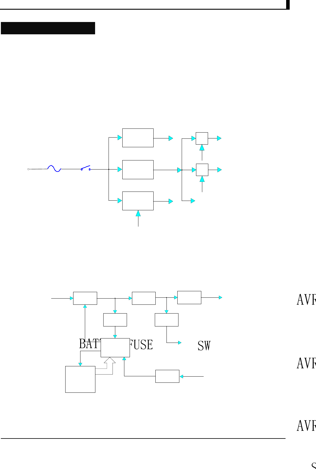
Circuit Description
1. Power Supply
Power supply of the radio is derived from the battery, which supplies battery B+ after passing through
fuse 3A and then feeds through power switch. The power supplies voltage for three AVRs. IC504
supplies 5V (M5V) voltage for the control circuit. And IC503 supplies 5V (C5V) voltage for the shared
circuit. IC502 supplies voltage for the transmit/receive circuit. In transmit mode, T5C becomes low
voltage and Q502 is turned on to supply 5V (T5v) voltage for the transmit circuit. In receive mode, R5C
becomes low voltage and Q504 is turned on to supply 5V (R5V) voltage for the receive circuit.
Fig. 1 Power Supply Block Diagram
2. PLL Frequency Synthesizer
PLL circuit generates the first local oscillator signal for reception and RF signal for transmission.
Fig.2 PLL Block Diagram
TC-700 Circuit Description
11
1) PLL Circuit
Step frequency of PLL can be 2.5 KHz, 5.0 KHz or 6.25 KHz. A 16.8MHz reference oscillator signal is
divided at IC301 by a counter to generate a 2.5 KHz, 5.0 KHz or 6.25 KHz reference frequency. Output
signal from VCO is buffer amplified by Q301 and divided at IC301 by a frequency divider. The divided
signal is compared with 2.5 KHz, 5.0 KHz or 6.25 KHz reference signal in the phase comparator of IC301.
The output signal from phase comparator is filtered through a low pass filter to generate a level D.C., and
the level D.C. controls oscillator frequency by controlling VCO.
2) VCO
The operating frequency is generated by Q302 in transmit mode and by Q307 in receive mode.
Operating frequency generate a control voltage by phase comparator to control varactor diodes so that
the oscillator frequency is consistent with the MCU preset frequency(D301、D302、D303 and D304 in
transmit mode, and D307、D308、D309 and D310 in receive mode). T/R pin is set high level in receive
mode, and low level in transmit mode. The output from Q302 and Q307 is amplified by Q304 and sent to
buffer amplifier.
3) Unlock Detector
An unlock condition appears if low level appears at MUXOUT pin of IC301. Transmission is forbidden if
this condition is detected by microprocessor.
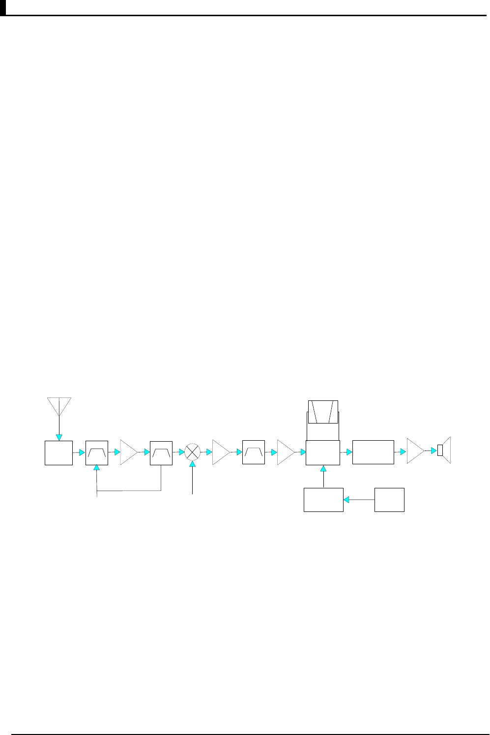
3. Receiver
The receiver utilizes double conversion superheterodyne (UHF)/(VHF).
Fig. 3 Receiver Section Configuration
1) Front-end RF Amplifier
The signal from antenna is amplified at RF amplifier (Q207) after passing through a
transmit/receive circuit and a band pass filter. Before passing the first mixer, the amplified
signal is filtered through another band pass filter to remove unwanted signals.
2) First Mixer
The signal from RF amplifier is mixed with the first local from PLL frequency synthesizer circuit at the fix
mixer (IC202) to create a 49.95MHz first IF signal. The first IF signal is then fed through a crystal filter
(XF203) to further remove unwanted signals.
TC-700 Circuit Description
12
3) IF Amplifier
The first IF signal is amplified by Q206 before passing through crystal filter and by Q204 after crystal
filter and then enters IF processing chip IC204. The signal from IC204 is mixed with the second oscillator
signal again in IC204 to create a 450 KHz second IF signal. The second IF signal then passes through a
450KHz ceramic filter (wideband: CF201,narrowband: CF202) to eliminate unwanted signals before it is
amplified and detected in IC204.
4) Narrowband/Wideband Switch Circuit
Pin WCON and NCON of IC500 outputs wideband (high level) and narrowband (low level) controlling
signal respectively to turn on corresponding diode-connector, and to choose ceramic filter CF201
(wideband) or CF202 (narrowband) to filter useless spurious signal.
5) AF Amplifier
The resulting AF signal from IC204 enters base band processing chip IC408. The processed AF signal is
then amplified by an AF power amplifier (IC401) to drive the speaker.
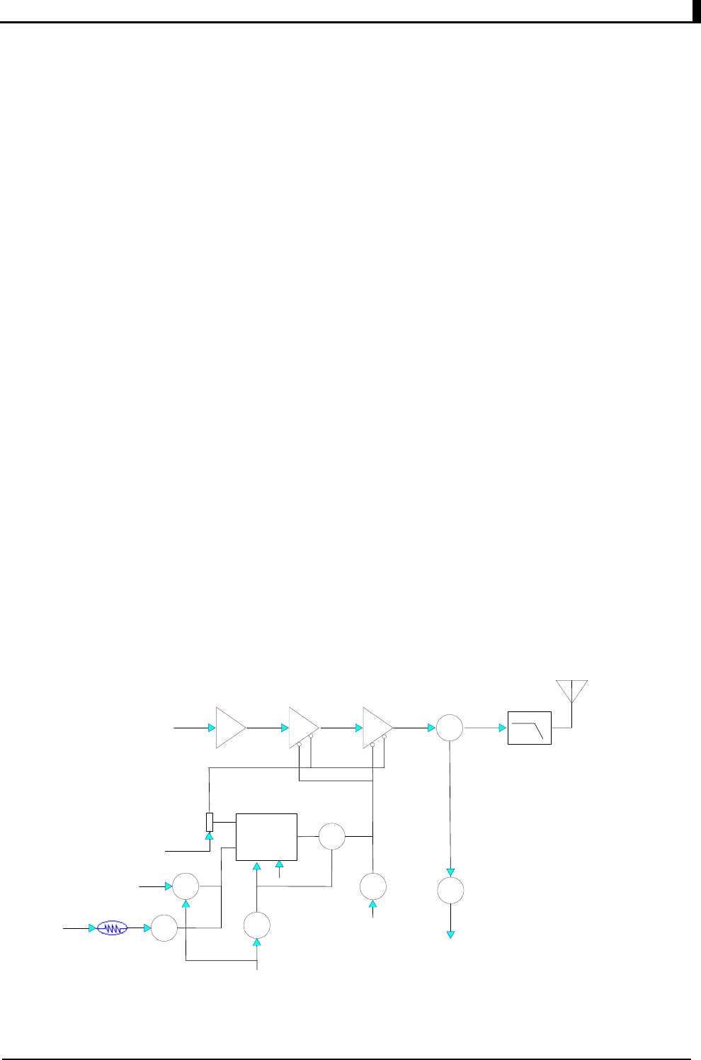
4. Transmitter
1) AF and Signaling
AF signal from the microphone is amplified and low-pass-filtered in IC402 before it enters base band
processing chip IC408, which also enters CTC/CDC/DTMF/2-Tone/5-Tone etc signaling generated by
CPU. The IC408 processed mixing signal enters VCO for direct FM modulation (see fig.5).
2) RF Power Amplifier
The transmit signal from VCO buffer amplifier (Q111) is amplified by Q101 and Q102. The amplified
signal is then amplified by the power amplifier Q103 and Q104 (including a two-stage FET amplifier) to
create 4.0W (UHF)/5.0W (VHF) RF power (see Fig. 6).
Fig. 4 APC System
TC-700 Circuit Description
13
3) Antenna Switch and LPF
Output signal from RF amplifier passes through a low-pass filter network and a transmit/receive switch
circuit comprised of D102,D103 and D104 before it reaches the antenna terminal. D103 and D104 is
turned on (conductive) in transmit mode and off (isolated) in receive mode.
4) APC
The automatic power control (APC) circuit stabilizes the transmit output power by detecting the drain
current of final stage amplifier FET. IC101 (2/2) compares the preset reference voltage with the voltage
obtained from final current. APC voltage is proportional to the difference between auto detect voltage
and reference voltage output from IC101 (1/2). The output voltage controls FET power.
5. Base Band and Signaling System
The block diagram of signaling section is shown as figure 5.
Fig. 5 AF and Signaling Circuit
1) CTC/CDC
Transmit: CTC/CDC signaling produced by CTC_PLL pass a low pass filter and then enters
VCXO. CTC/CDC signaling produced by CTC_OUT pass a low pass filter and then
mixed with AF before enters VCO.
Receive: Demodulated signal enters MCU after pass IC404、IC405. MCU then judges whether
CTC/CDC matches the preset values or not. According the result, the out tone will be
controlled by AFMUTE.
2) 2-Tone / 5-Tone and DTMF
Transmit: The signal produced by MCU provides a TX and SP out tone, and is then applied to
the base band processing IC. The signal in mixed with the audio signal and goes to
the VCO。
Receive: Demodulated signal is filtered after passing base band processing IC, and then enters
MCU for decoding.
TC-700 Circuit Description
14
3) MSK
Transmit: MSK signal produced by base band processing IC enters VCO together with AF
signal for modulation.
Receive: MSK input of demodulating IC is sent to AK2346 for demodulation after being
amplified. The demodulated signal is then sent to MCU for decoding.
4) AF
Transmit: AF signal from MIC enters base band processed IC for amplification, pre-emphasis
etc. after being amplified. And then it enters VCO for modulation.
Receive: Demodulated AF signal enters the base band processing IC for amplification,
de-emphasis etc. after being amplified. And then it enters AF power amplifier drived
speaker.
Base band processed chip provides functions for processing signal as amplifying,
filtering, emphasizing, scrambling, companding, and amplitude limiting.
6.Control System
The IC500 CPU operates at 9.8304 MHz.
The block diagram of MCU control system is shown as following:
Fig.6 MCU Block Diagram
Circuit in this section is mainly comprised of MCU, EEPROM etc.
MCU control circuit accomplishes the following functions: accomplish the reset initialization according to
the programmed feature of the radio when power on; detect keying signal and monitor battery voltage;
send necessary frequency data to PLL according to encode of the channel; switch and control
transmit/receive according to the signal input from PTT; turn on/off the mute circuit according to the input
signaling decode signal and squelch level signal; output control signal to control the light/off of LED;
control signaling process IC to perform tasks.
EEPROM

TC-700 CPU Pins
15
CPU Pins
1. CPU pins are as follows:
No. MCU Port Name Port Name Input/Output Features
1 P94/DA1 APC/TV O Automatic Power Control
2 P93/DA0 TONEO O DTMF/2-5Tone/Beep tone output/ ALARM
tone output
3 P92/TB2IN NC O NC
4 P91 O
5 P90 SHIFT O Clock beat-frequency
6 BYTE BYTE I
7 CNVSS CNVSS I
8 P87/XCIN O
9 P86/XCOUT O
10 RESET RESET I Input low level to enter all reset mode
11 XOUT XOUT O Crystal oscillator output pin
12 VSS GND I GND
13 XIN XIN I Crystal oscillator output pin
14 VCC VCC I VCC
15 P85/NMI NMI I
16 P84/INT2 AFCK I 2346 TCLK
17 P83/INT1 AUX1 O Indication for external scrambler
18 P82/INT0 AFRDF I 2346 RDF
19 P81 O
20 P80 PTTCO O PTTCO
21 P77 NC O
22 P76/TA3O CTCOUT O CTC _OUT (PWM) TO VCO
23 P75 NC O
24 P74/TA2O CTC_PLL O CTC_PLL (PWM)
25 P73 AUX2 COM5 Indication for receive/transmit status
26 P72/TA1O 1/2OSC O
27 P71/RxD2/TB5IN TONEI O
28 P70/TxD2
29 P67/TxD1 TXD O Serial date output.
30 P66/RxD1 RXD I Serial date input.
31 P65 I
32 P64 O
33 P63/TxD0 I COM4 MANDOWN Input Pin
34 P62/RxD0 O COM3

TC-700 CPU Pins
16
35 P61 COM1
36 P60 COM2
37 P57/RDY EEDAT I/O EEPROM DATA, date input/output.
38 P56/ALE EECLK O EEPROM CLK
39 P55/HOLD
40 P54/HLDA AFDIR O AK2346 DIR
41 P53/BLCK AFSCK O 2346 SCLK
42 P52/RD NC O
43 P51/BHE AFDT O 2346 TDATA
44 P50/WR WE I
45 P47/CS3 CODIO I/O Common date control (AK2346 DATA).
46 P46/CS2
47 P45/CS1 SAVE O SAVE, power save control
48 P44/CS0 R5C O R5C Rx circuit power supply control
49 P43/A19 T5C O T5C Tx circuit power supply control
50 P42/A18
51 P41/A17
52 P40/A16
53 P37/A15
54 P36/A14
55 P35/A13
56 P34/A12
57 P33/A11
58 P32/A10
59 P31/A9
60 Vcc VCC I VCC
61 P30/A8 NCON O Narrowband control
62 Vss GND I GND
63 P27/A7 AFCO O AFCO
64 P26/A6 WCON O Wideband control
65 P25/A5 LEDR O Red light control:H,lit;L,out
66 P24/A4 LEDG O Green light control:H,lit;L,out
67 P23/A3 EN2 I EN2
68 P22/A2 EN4 I EN4
69 P21/A1 EN3 I EN3
70 P20/A0 EN1 I EN1
71 P17/INT5
72 P16/INT4 AFMUTE

TC-700 CPU Pins
17
73 P15/INT3
74 P14 TK I Top Key
75 P13 DC-Switch O
76 P12 PLL_UL I PLL unlock detect
77 P11 PLL_STB O PLL strobe output
78 P10 MICMUTE O MICMUTE
79 P07/D7 Option1 I Programming cable detect.
80 P06/D6 PLL_DATA O PLL date input
81 P05/D5 PLL_CLK O PLL clock output
82 P04/D4 T/R O Receive/transmit control
83 P03/D3 APC-Switch O
84 P02/D2 PTT I PTT
85 P01/D1 SK1 I Side Key1
86 P00/D0 SK2 I Side Key2
87 P107/AN7 I MIC signal input
88 P106/AN6 BATT I BATT, battery voltage detect
89 P105/AN5 BATTSEL I Battery detect
90 P104/AN4 NC I
91 P103/AN3 SELF I Reset mode control:ground this pin to enter
reset mode.
92 P102/AN2 RSSI I RSSI detect pin
93 P101/AN1 SQL I Squelch level input
94 AVSS GND I A/D conversion power supply input.
95 P100/AN0 CTCIN I CTCSS output
96 VREF VCC I A/D conversion reference voltage
97 AVCC VCC I A/D conversion power supply input.
98 P97 O
99 P96 O
100 P95 O

TC-700 Part List 1
18
TC-700 Part List 1
TC-700 Adjustment Description
19
Adjustment Description
Adjust the radio by PC programming software or by manual adjustment. In manual adjustment mode, the
adjustment method is shown as follows: (Refer to “Software Specification” for the manual adjustment
mode)
Required Test Instrument
Radio Communication Test Set 1 set
Scanner 1 set
3A/10V Power Supply 1 set
Digital Voltmeter 1 set
3A Ammeter 1 set
Adjustment
1. Adjustment in user mode
Firstly ground the SELF point, turn on the power by holding down TK for 2 seconds, and then the radio
enters reset mode with green LED flashing twice. Turn the channel selector knob to the selected channel
and press PTT, the radio data is all reset (All clone modes will be automatically activated when reset is
completed). Refer to All Reset Mode in Software Specification for more details:
VCO
Measurement Adjustment
Item Condition Test
Instrument Terminal Parts Method
Specification
/Remarks
1. Setting Power supply voltage
1. CH: TX high 3.9V±0.1V 2.Transmit VCO
lock voltage 2. TX Low Check >0.5V
1. CH: RX high 3.9V±0.1V 3.Receive VCO
lock voltage 2. RX low
Digital
Voltmeter
CV TC301
TC302
Check >0.5V
2. Manual Adjust Mode Description
(1) Enter the manual adjust mode
Turn the power on by holding down TK and SK2 key simultaneously for 2 seconds, the radio enters
manual adjust mode with red LED flashes twice. (TK: Top key; SK1: Side key1; SK2: Side key2)
(2) Channel number on the channel selector knob
Each channel number on the channel selector knob is defined a setting item. The bandwidth is
25 KHz and low frequency (F1) each time the channel selector knob is rotated.

TC-700 Adjustment Description
20
(3) SK2 key
Used to set the frequency. 1 point tuning is used to adjust center frequency, 3 point tuning adjusts
F1, F3, F5 and 5 point tuning adjusts F1-F5. The frequency toggles from low frequency to high
frequency. Green LED flashes once when F1 is selected.
(4) TK key
Use to toggle the channel bandwidth among 25 KHz, 20 KHz and 12.5 KHz. Red LED flashes once
when the bandwidth is 25 KHz.
(5) PTT/SK1
PTT→Increase
SK1→Decrease
PTT/SK1 is pressed to adjust upward/downward. Red LED glows indicating the maximum adjust
value and green LED indicating the minimum value. Hold down the key to increase/decrease the
adjust value continuously.
Press PTT key to save the BATT LOW and SQL settings, then green LED glows once.
(6) Select adjustment item group
The first group of adjustment item is selected when the radio enters the manual adjust mode.
Turn to CH16 and press PTT key to enter the next group. Press again to return to the first group.
Orange LED flashes once when the first group is selected. Orange LED flashes twice when the
second group is selected.
(7) Frequency Setting (can be set via programming software)
5 point tuning(MHz) TX: { TX1,TX2,TX3,TX4,TX5}
RX: {
RX1,RX2,RX3,RX4,RX5}
3 point tuning(MHz) TX: { TX1, TX3, TX5}
RX: {
RX1, RX3, RX5}
1 point tuning(MHz) TX: { TX3}
RX: {
RX3}

TC-700 Adjustment Description
21
3. Adjustment Method
Turn the power on by holding down TK and SK2 key simultaneously for 2 seconds, the radio enters
manual adjust mode with red LED flashes twice. Refer to Manual Adjust Mode in TC-700 Software
Specification for more details.
(1) Transmitter
Item Condition Test Instrument Method Purpose
Adjust a channel
Enter the adjust mode;
Turn to CH1;
TX mode.
Radio
Communication
Test Set;
TX Test
Adjust
VR1
Frequency Error
≤100Hz
1. TX power Low
Enter the adjust mode.
Turn to CH1.
Adjust at 5 point
(wideband).
PTT key
(increase)
SK1 key
(decrease)
Adjust power to:
1W±0.1W
2. CDCSS balance
Enter the adjust mode.
Turn to CH3. Adjust at
3 point (wideband), 1 point
(medium band) and
1 point (narrowband)
respectively.
PTT key
(increase)
SK1 key
(decrease)
No adjustment
3. CDCSS
deviation
Enter the adjust mode.
Turn to CH3. Adjust at
3 point (wideband), 1 point
(medium band) and
1 point (narrowband)
respectively.
PTT key
(increase)
SK1 key
(decrease)
4. CTCSS (67.0Hz)
deviation Low
Enter the adjust mode.
Turn to CH4. Adjust at
3 point (wideband), 1 point
(medium band) and
1 point (narrowband)
respectively.
PTT key
(increase)
SK1 key
(decrease)
Group 1
5. CTCSS
(136.5Hz) deviation
Center
Enter the adjust mode.
Turn to CH5. Adjust at 3
point (wideband), 1 point
(medium band) and
1 point (narrowband)
respectively.
Radio
Communication
Test Set
TX TEST
HPF:20HZ
LPF:300HZ
PTT key
(increase)
SK1 key
(decrease)
Adjust deviation to
750Hz (wideband),
600Hz (medium
band) and 400Hz
(narrowband)
respectively.

TC-700 Adjustment Description
22
6. CTCSS
(254.1Hz)
deviation
High
Enter the adjust mode.
Turn to CH6. Adjust at 3
point (wideband), 1 point
(medium band) and 1
point (narrowband)
respectively.
PTT key (increase)
SK1 key
(decrease)
7. AK2346
Transmit
Audio
Deviation
Enter the adjust mode.
Turn to CH7. Adjust at 3
point (wideband), 1 point
(medium band), 1 point
(narrow band).
Radio
Communication
Test Set
HPF: 20Hz
LPF: 15KHz
1KHz
120mV
PTT key (increase)
SK1 key
(decrease)
Adjust deviation to
4KHz (wideband),
3.2KHz (medium
band) and 2KHz
(narrowband)
respectively.
8. 2 Tone
deviation
Enter the adjust mode.
Turn to CH8. Adjust at 1
point (wideband), 1 point
(medium band), 1 point
(narrow band).
PTT key (increase)
SK1 key
(decrease)
Adjust deviation to
3.2KHz
(wideband),
2.5KHz (medium
band) and 1.8KHz
(narrowband)
respectively.
9. DTMF
deviation
Enter the adjust mode.
Turn to CH9. Adjust at 1
point (wideband), 1 point
(medium band), and 1
point (narrow band).
PTT key (increase)
SK1 key
(decrease)
Adjust deviation to
3.2KHz
(wideband),
2.5KHz (medium
band) and 1.8KHz
(narrowband)
respectively.
Group 1
10. MSK
deviation
Enter the adjust mode.
Turn to CH10. Adjust at 3
point (wideband), 1 point
(medium band), 1 point
(narrow band).
Radio
Communication
Test Set
TX Test
HPF: 20Hz
LPF: 15KHz
No modulation
signal.
PTT key (increase)
SK1 key
(decrease)
Adjust deviation to
3.2KHz
(wideband),
2.5KHz (medium
band) and 1.8KHz
(narrowband)
respectively.

TC-700 Adjustment Description
23
11. TX power
HIGH
Enter the adjust mode.
Turn to CH13. Adjust at 5
point (wideband).
PTT key (increase)
SK1 key (decrease)
Adjust power to
5W(4W)±0.1W
VHF: 5W,
UHF: 4W
Group 1
12. TX voltage
Low
Enter the adjust mode.
Turn to CH14. Adjust at 1
point (wideband).
Radio
Communication
Test Set
TX TEST
Save
Adjust voltage to
5.8V,press PTT to
save

TC-700 Adjustment Description
24
Receiver
Item Condition Test
Instrument
Method Purpose
1. RX
sensitivity
Enter the adjust mode. Turn to
CH1.
Adjust at 5 point (wideband).
PTT key
SK1 key
Adjust level to
119dBm.
SINAD≥12dB
2. AK2346 RX
volume
Enter the adjust mode. Turn to
CH2. Adjust 1 point at
wideband, medium band and
narrowband respectively.
PTT key
(Increase)
SK1 key
(Decrease
When Max. volume
is set, adjust AC
level to 1W (16Ω),
single input 2.5V,
dual input 5V
3. Squelch
Level 3
(OPEN)
Enter the adjust mode. Turn to
CH3. Adjust at 5 point
(wideband), 1 point (medium
band) and 1 point
(narrowband) respectively.
Save
Adjust level to
-123dBm,press
PTT to save
4. Squelch
Level 3
(SQUELCH)
Enter the adjust mode. Turn to
CH4. Adjust at 5 point
(wideband), 1 point (medium
band) and 1 point
(narrowband) respectively.
Save
Adjust level to
-125dBm,press
PTT to save
5. Squelch
Level 9
(OPEN)
Enter the adjust mode. Turn to
CH5. Adjust at 5 point
(wideband), 1 point (medium
band) and 1 point
(narrowband) respectively.
Save
Adjust level to
-117dBm,press
PTT to save
6. Squelch
Level 9
(SQUELCH)
Enter the adjust mode. Turn to
CH6. Adjust at 5 point
(wideband), 1 point (medium
band) and 1 point
(narrowband) respectively.
Save
Adjust level to
-119dBm,press
PTT to save
Group 2
7. RX voltage
Low
Enter the adjust mode. Turn to
CH7. Adjust at 1 point
(wideband).
Radio
Communication
Test Set
RX TEST
HPF:300HZ
LPF:3KHZ
Save
Adjust power
supply voltage to
6.3V, press PTT to
save
Note: AF deviation of the receiver is 3KHz (wideband),2.5KHz(medium band) and 1.5KHz (narrowband)
TC-700 Disassembly and Assembly for Repair
25
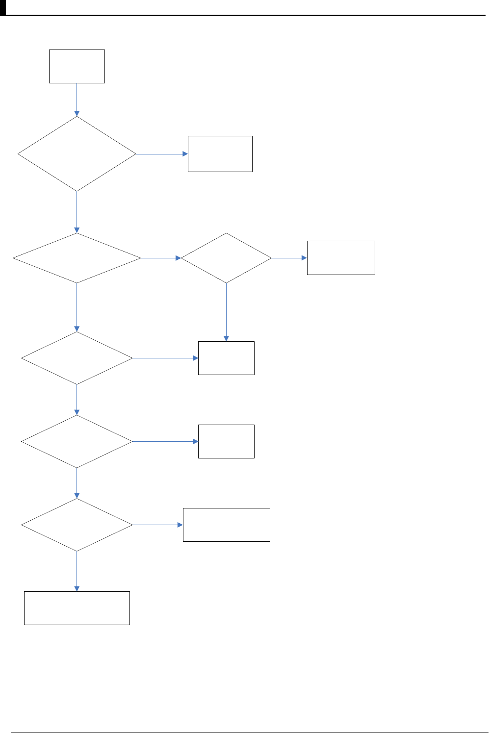
Trouble-shooting Chart
Normal power-on
alert tone?
MCU Check
The RF circuit can’t
be driven.
Yes
Speaker works
well?
NO
Replace
the speaker
NO
`
9.8304MHz works
normally?
Yes
Read
available?
Yes
Q501
works well?
Exchange
Q501
NO
Check M5V
MCU works well
Pin10 is of
high level?
Yes
Yes
Yes
Check the
control circuit
NO Check the
circuit of read
frequency
Yes Reset
NO
TC-700 Disassembly and Assembly for Repair
26
Power supply is
normal?
VCO
Check
Exchange
Q306
NO
Oscillator CV voltage in
Rx is normal?
Yes
Check if Q305
works well.
NO NO
`
Check if Q304
output normally?
Yes
Exchange
Q305
Check
Q304
NO
Yes
Check if feedback
is normal.
Check
Q301
NO
Check power
supply circuit.
Check CPU data
circuit
Check if 16.8MHz
oscillates?
Yes
Yes
Yes
NO
TC-700 Disassembly and Assembly for Repair
27
No output
power
Power supply
works well?
Check power
supply circuit
Check Q502
Check drive
stage
Check transistor offset
voltage and low pass
network
Repair the
transmissio
n network
Check the
suited
network
VCO
Check flow
chart
Exchange
Q102
Exchange
Q101
Finished
Finished
Finished
Control voltage is
normal?
The current is
normal?
Driver stage is
normal?
The power is
normal?
If the power
is normal.
If the power
is normal.
NO
Yes
NO Low
High
Yes
NO
NO
Yes
Yes
Yes
Yes
NO
NO
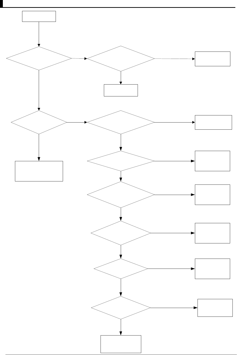
TC-700 Disassembly and Assembly for Repair
28
Check if the power
supply of AF IC is
normal?
No recieve
Check if the output
of base band IC is
normal.
Check if control voltage
AFCO is normal.
Check if the input of
base band IC is normal.
Exchange
AK2346
Check the output of
IC204 is normal.
Check the second local
oscillator is normal.
Check the voltage of
CD201 is normal.
Check if PIN 16
outputs in IF input
Check if T1 outputs in
RF input
Exchange
CD201
Check Q308
Check IC404
Exchange IC
Exchange 717
Check the
status of IC204
Check VCO
Check volume knob
& AFMUTE
Yes
NO
NO Yes
NO
NO
NO
NO
NO
NO
Yes
Yes
Yes
NO
Yes
Yes
Yes
Check Q207
passage
Yes
TC-700 Disassembly and Assembly for Repair
29
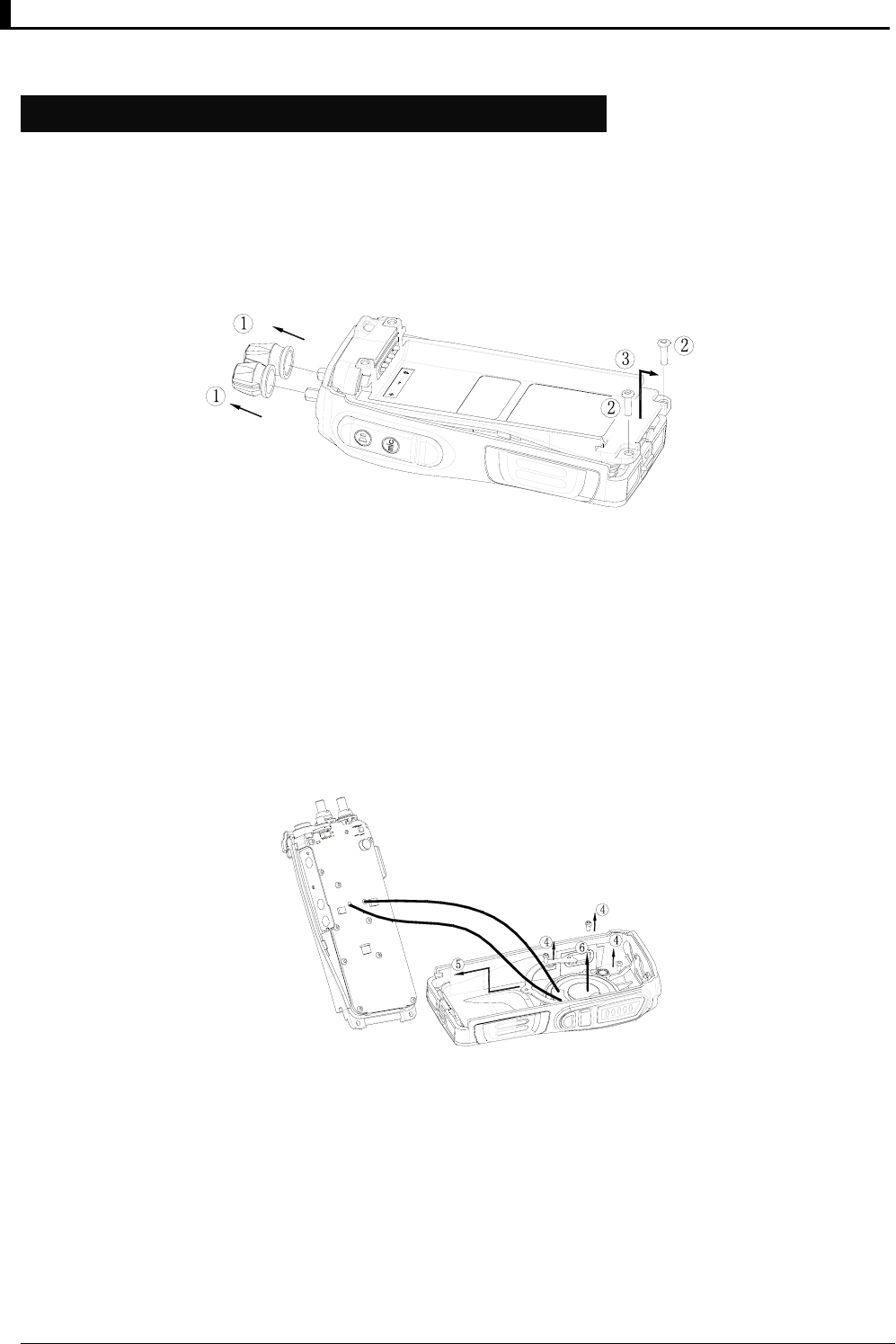
Disassembly and Assembly for Repair
1. Remove the case assembly from the chassis (as shown in Fig. 1)
1. Remove the volume knob and channel knob①.
2. Remove the two screws ②.
3. Lift the both sides of chassis from the case assembly ③.
Fig. 1
2. Remove the speaker (as shown in Fig. 2)
1. Remove the three screws on the fixing ring of the speaker ④ and take out the fixing ring ⑤.
Note: be careful not to snap the speaker’s lead wire.
2. Take out the speaker and water-proof gasket ⑥.
Fig. 2
3. Removing the Tx-Rx unit from the chassis (as shown in Fig. 3)
1. Loosen the nut on channel switch ⑦ and that on volume switch ⑧, and remove earphone
holder ⑨.
2. Remove the screw ⑩ on the PTT key board.
3. Remove the ten screws ⑾ fixing the control board.
4. Remove the solder of the antenna terminal with a soldering iron ⑿.
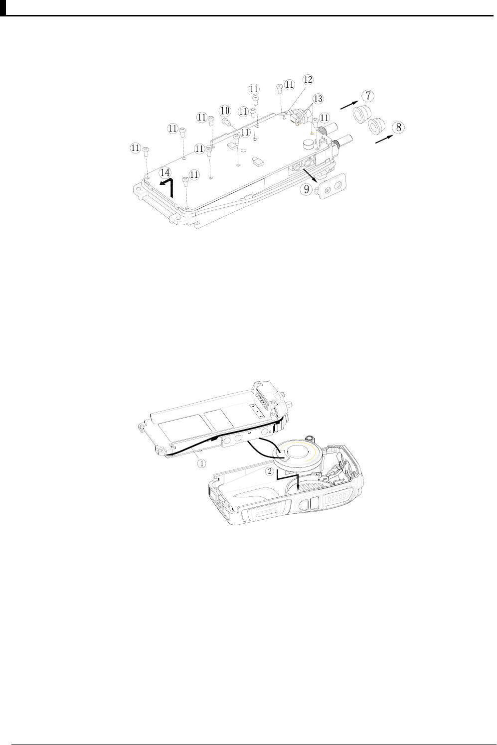
TC-700 Disassembly and Assembly for Repair
30
5. Remove the solder of the positive and negative terminal on the battery’s connector with a
soldering iron ⒀.
6. Lift and remove the main unit board ⒁ from the chassis.
Fig. 3
Cautions for assembly:
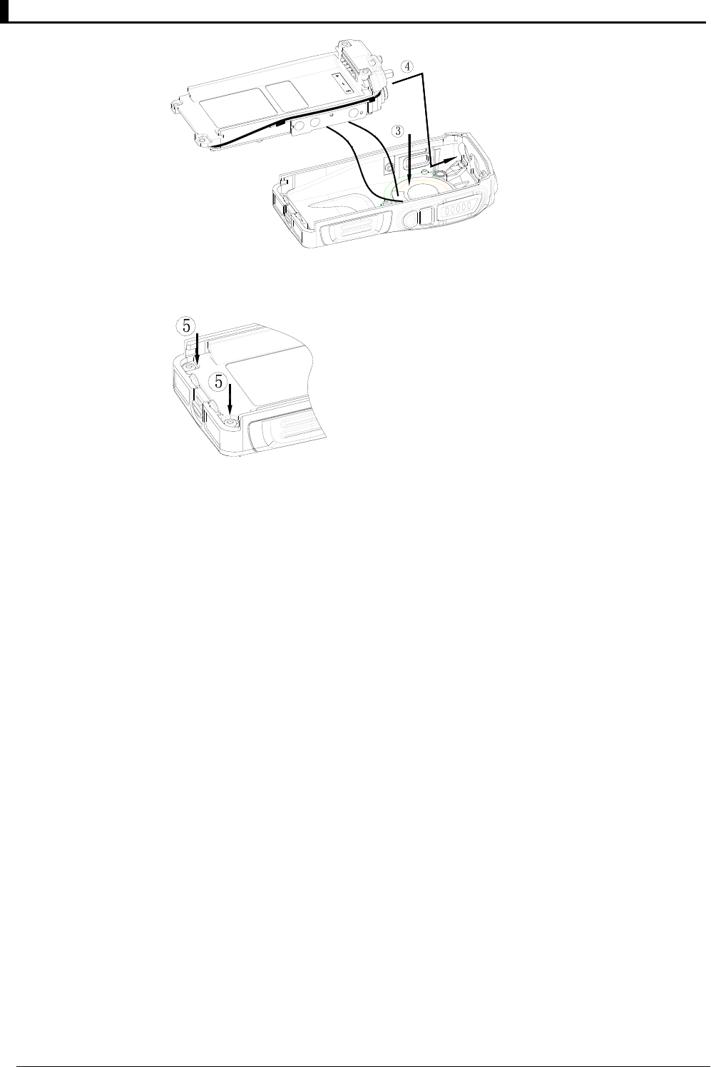
4. Attaching the case assembly and chassis (as shown in Fig. 4, 5 & 6)
1. Make sure the water-proof packing attached to the circumference of the chassis is securely
inserted in the groove of the chassis ①.
2. Attach speaker and its water-proof ring to the corresponding place on the chassis ②.
Note: ensure the speaker and the ring is securely inserted.
Fig. 4
3. Press the stainless fixing ring on the water-proof packing of the speaker, and attach the screw ③.
4. Insert the upper part of the chassis into the case assembly ④.
Note: Make sure the speaker lead wire does not press on the microphone magnetic core.
5. Press downward the chassis ⑤, enabling the chassis and the case to fit together.
Note: If the packing of the SP/MIC does not come to the correct position after attaching the
chassis to the case assembly, reposition the packing with your fingers.
TC-700 Disassembly and Assembly for Repair
31
Fig. 5
Fig. 6
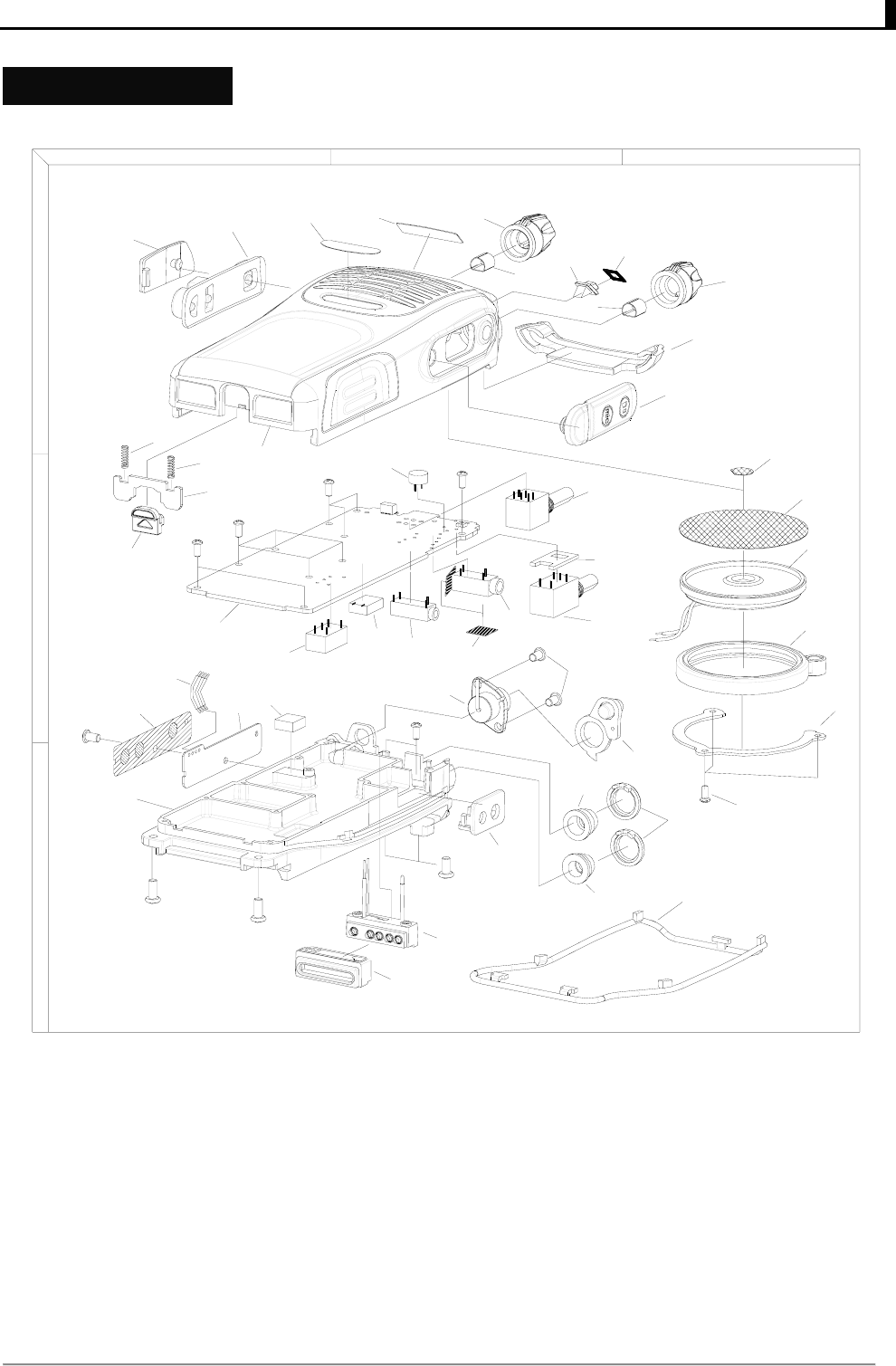
TC-700 Exploded View
44
Exploded View
16
9
10
15
19
20
21
22
28 29
30
41
A
42
42 43
2
B
A
1
C
14
35 34
33
32
31
11
A
23
24
12345
7
6
12
13
17
18
B
40
39
38
26
E
D
A
A
A
FC
E
6
TX-RX Unit
27
37 36
25
8
TC-700U(2) Part List 2
46
TC-700 Part List 2
No. P/N Part Description Qty
1 6000135000000 TC-700S PTT key cover Black 1.00
2 6100068000000 TC-700S PTT silica rubber key Black 1.00
3 8600700500000 TC-700 Model label 1.00
4 8600700500100 HYT-LOGO Logo 1.00
5 6000076000020 TC700 Knob (encoder) 1.00
6 6201006000000 TC2088 Inner liner knob 2.00
7 6000136000000 TC-700S Light guide 1.00
8 750700S000000 TC700S Light guide 3M (9448) adhesive paper 1.00
9 6000077000020 TC700 Knob (volume) 1.00
10 6000134000000 TC-700S Rear cover (main unit) 1.00
11 6000138000000 TC-700S Dust-proof cover 1.00
12 7400051000000 TC700S Mic mesh 1.00
13 7400054000000 Speaker mesh 1.00
14 5001040000000 Speaker 16Ω 1W D: 40mm 1.00
15 6100066000000 TC-700S Water-proof gasket (speaker) 1.00
16 6201078000000 TC-700S Stainless fixing ring (speaker) 1.00
17 7207005400000 Nut M7.0*5.4mm 1.00
18 7206004200000 Nut M6.0*4.2mm 1.00
19 6100069000000 TC-700S Water-proof gasket (volume knob) 2.00
20 6100065000000 TC-700S Water-proof gasket (main unit) 1.00
21 6100070000000 TC-700S Water-proof gasket (battery connector) 1.00
22 5202003100010 TC-700S 3P battery connector socket 1.00
23 6000137000000 TC-700S Mic holder Black 1.00
24 6300016000000 TC-700S Aluminum chassis 1.00
25 7300001000000 TC700S PTT metal dome (3-key) 1.00
26 4210047000000 TC-700 Key board connection cable 47mm 0.50
27 4100700101100 TC-700S PT PCB FR4 0.6T/2L 1.00
28 7500114000000 TC500 Gap pad 1.00
29 4400000000000 SMA-type MSMA1551D5-001-NT3G-50 connector Male 1.00
30 6100067000000 TC-700S Antenna water-proof gasket 1.00
31 5002110000020 Mic cover CZII-T6027P-C33 -60dB±3dB φ6.0*2.27 1.00
32 4304030000010 Gray-code encoder switch 1.00
33 7500044000000 TC700 Volume switch pad 1.0mm-thick 1.00
34 4302020000040 Volume switch TC3000 TP76N17N 15F(A103) 1.00
35 5205000000280 Speaker jack HSJ1456-010320 1.00
36 7400023000010 TC-500 PVC sheet 0.2mm-thick 2.00
37 5205000000190 Earpiece jack HSJ1650-010020 1.00
38 3920450300000 Demodulator plug-in 450KHz±4kHz 1.00
39 3801045030090 Ceramic filter 450KHz±6.0KHz 1.00
40 6000128000000 TC-700 Battery latch Black 1.00

TC-700U(2) Part List 2
46
41 6201078000000 TC-700S Battery latch baffle 1.2mmSUS304 1.00
42 7000036000000 TC-700S Spring Ф0.35*Ф2.3*10mm 2.00
43 6000133000000 TC-700S Main unit front case Black 1.00
A 7101904020020 Self-tapping ST1.9*4.0mm 13.00
B 7102504000300 Machine screw M2.5*4.0mm Ultra-thin cross-head 2.00
C 7102004520000 Self-tapping ST2.0*4.5mm pan head 2.00
D 7103006001000 Machine screw M3.0*6.0mm pan head 2.00
E 7102508000000 Machine screw M2.5*8.0mm Hex wobbler 2.00
F 7102004020050 Self-tapping ST2.0*4.0mm cross recessed pan head 1.00
TC-700 Packing
47
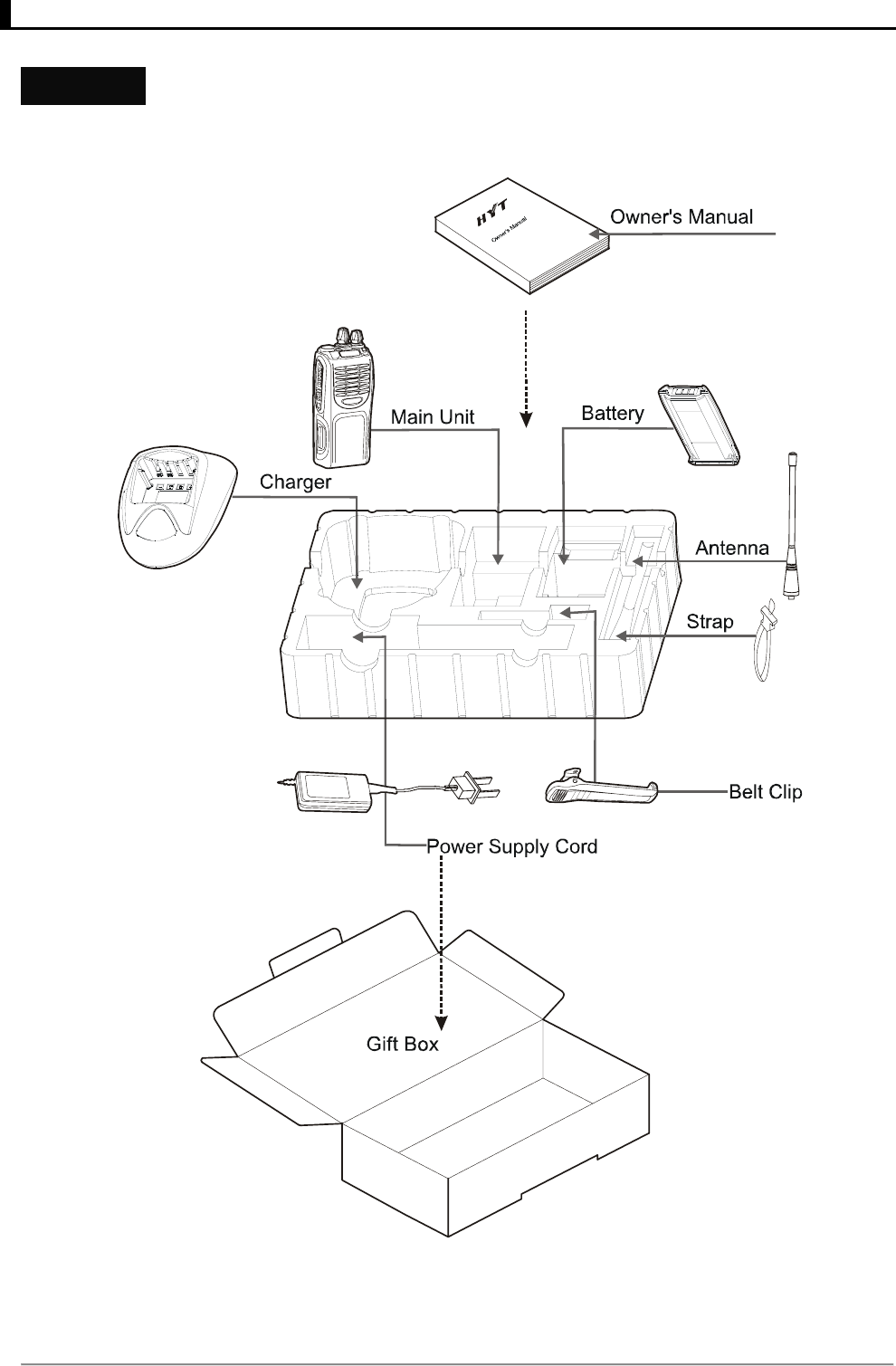
Packing
Description of TC-700 Desktop Charger
56
Description of TC-700 Desktop Charger
Ⅰ. General Description
The charger is developed & designed for TC-700 wireless series. The charger adopts bq2000T——a
programmable multi-chemistry fast-charge management IC.
The charger is for fast-charge management of nickel cadmium (Ni-Cd), nickel metal-hydride (Ni-MH), or
lithium-ion (Li-Ion) batteries in single or multi-chemistry applications.
High-frequency switching controller for efficient and simple charge design, provides over 90% efficiency
rating.
Ⅱ. General description of bq2000T functions
The bq2000T detects the battery chemistry and proceeds with the optional charging and termination
algorithms. This process eliminates undesirable undercharged or overcharged conditions and allows
accurate and safe termination of fast charge.
Depending on the chemistry, the bq2000T provides a number of charge termination criteria:
z Peak voltage detection (PVD) (for NiCd and NiMH)
z Minimum charging current (for Li-Ion)
z Maximum temperature
z Maximum charge time
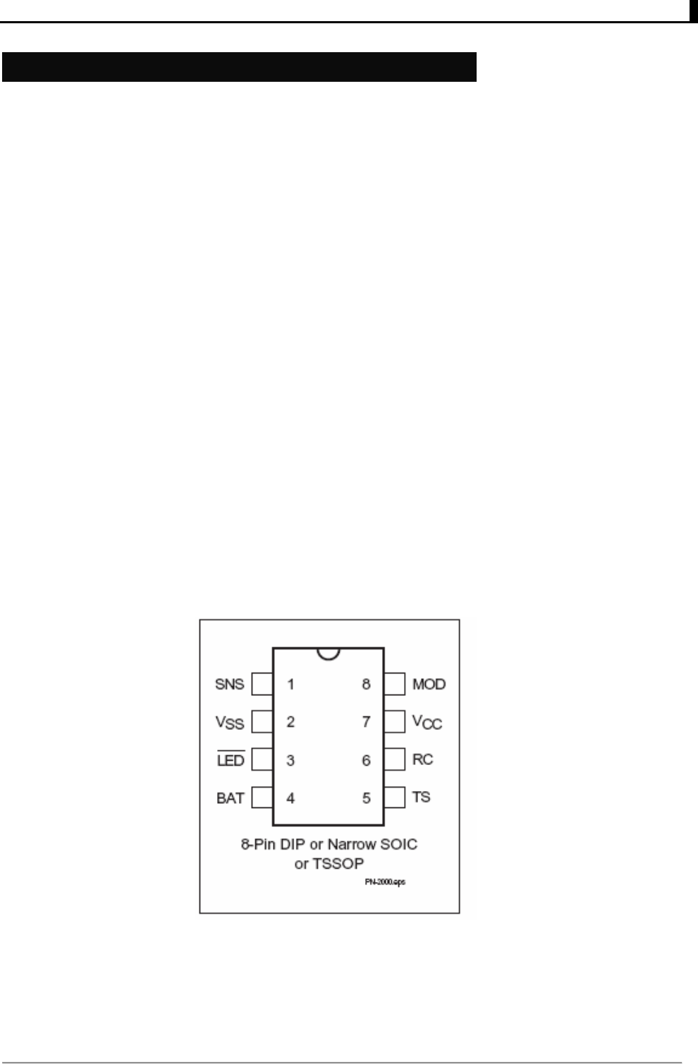
Pin Connections

Description of TC-700 Desktop Charger
57
Pin Names and Descriptions:
SNS: Current-sense input
Enables the bq2000T to sense the battery current via the voltage developed on this pin by an
external sense-resistor connected in series with the battery pack.
Vss: System ground
LED: Charge-status output
Open-drain output that indicates the charging status by turning on, turning off, or flashing an
external LED.
BAT: Battery-voltage input
Battery-voltage sense input. A simple resistive divider, across the battery terminals, generates
this input.
TS: Temperature-sense input
Input for an external battery-temperature monitoring circuit. An external resistive divider network
with a negative temperature-coefficient thermistor sets the lower and upper temperature
thresholds.
RC: Timer-program input
RC input used to program the maximum charge-time, hold-off period, and trickle rate during the
charge cycle, and to disable or enable top-off charge.
Vcc: Supply-voltage input
MOD: Modulation-control output
Push-pull output that controls the charging current to the battery. MOD switches high to enable
charging current to flow and low to inhibit charging current flow.
Description of TC-700 Desktop Charger
58
Charge Termination
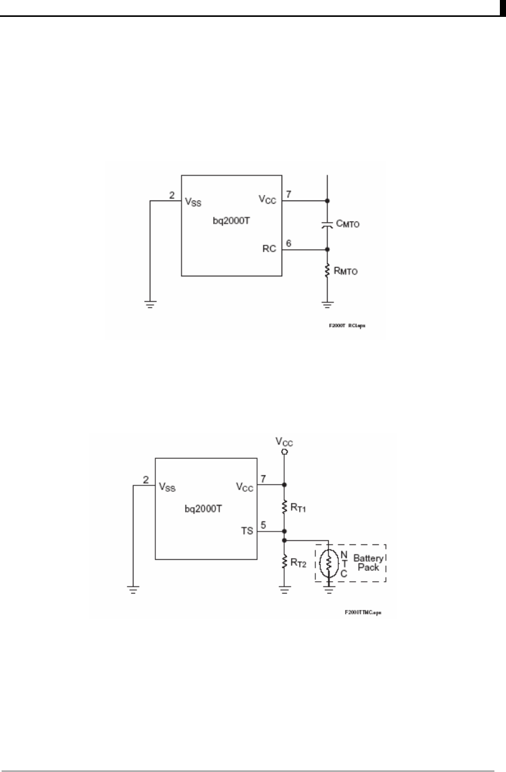
1. Maximum Charge Time (NiCd, NiMH, and Li-Ion)
The bq2000T sets the maximum charge-time through pin RC. With the proper selection of external
resistor and capacitor, various time-out values may be achieved. Figure Ⅱshows a typical
connection.
Figure Ⅱ Typical Connection for the RC Input
2. Maximum Temperature (NiCd, NiMH, and Li-Ion)
During fast charge, the bq2000T compares the battery temperature to an internal high-temperature
cutoff threshold, VTCO. As shown in Figure Ⅲ, high-temperature termination occurs when voltage
at pin TS is less than this threshold.
Figure Ⅲ Temperature Monitoring Configuration
3. Peak Voltage Detection (Ni-Cd, Ni-MH battery) (PVD)
bq2000T adopts PVD method to stop the charging of Ni-Cd and Ni-MH batteries. It continuously
samples the voltage of BAT pin which reflects the voltage of the whole battery. Bq2000T begins
PVD function if this voltage is less than the maximum sampling voltage 3.8mv (PVD). As shown in
Fig. IV, the resistor-divider between the anode of the battery clip and Vss pin determines the
voltage of BAT pin.
Description of TC-700 Desktop Charger
59
Figure Ⅳ Battery Voltage Divider
For Li-Ion battery packs, the resistor values RB1 and RB2 are calculated by the following equation:
Where N is the number of cells in series. The end-to-end input impedance of this resistive divider
network should be at least 200KΩ and no more than 1MΩ.
A NiCd or NiMH battery pack consisting of N series-cells may benefit by the selection of the RB1
value to be N-1 times larger than the RB2 value.
In a mixed-chemistry design, a common voltage divider is used as long as the maximum charge
voltage of the nickel-based pack is below that of the Li-Ion pack. Otherwise, different scaling is
required.
4. Charge Current Control
The bq2000T controls the charge current through the MOD output pin. The current-control circuit
supports a switching-current regulator with frequencies up to 500kHz. The bq2000T monitors charge
current at the SNS input by the voltage drop across a sense-resistor, RSNS, in series with the battery
pack. See Figure Ⅴ for a typical current-sensing circuit. RSNS is sized to provide the desired
fast-charge current (IMAX).
If the voltage at the SNS is lower than VSNSLO or higher than VSNSHI, the bq2000T switches the
MOD output high to pass charge current to the battery. When the SNS voltage is less than VSNSL or
greater than VSNSHI, the bq2000T switches the MOD output low to shut off charging current to the
battery.
Figure Ⅴ Current-Sensing Circuit

Description of TC-700 Desktop Charger
60
Ⅲ. Specifications
1. Output voltage and current
Input: 12±3V 1000mA
Output: 8-12V 20~1000mA
(Input: 12V 1000mA DC
Output: 800mA DC)
2. Charging current
1) Li-ion battery
Fast charging current: 800±200mA
Minimum charging current: 75±20mA
2) Ni-MH battery
Fast charging current: 850±100 mA
Supplementary charging current: 65±10mA
Trickle charging current: 25~35mA
IV. Charging process and indicator
1. Li-ion battery
1) Constant-current charging: charging current is 800±200mA and the indicator turns red. The
battery switches to constant voltage charging when the voltage rises to 8.4±0.1V.
2) Constant voltage charging: with 8.4±0.1V voltage and indicator turns red.
3) Completed: battery voltage: 8.4±0.1V; the minimum charging current drops to 75±20mA; LED
indicator turns green.
2. Ni-MH battery
1) Fast charge: current: 850±100mA; LED indicator: red; switch to supplementary charging when
rate of temperature rise dT/dt=0.9~1/min or the temperature rises to 50℃.
2) Supplementary charging: charging current: 65±10mA; LED indicator: green; switch to trickle
charging if the supplementary charging time reaches or exceeds MTO.
3) Trickle charging: charging current: 25~35mA; LED indicator: green.
TC-700 Specifications
64
Specifications
General
Frequency Range
VHF: 136-174MHz
UHF:300-350MHz,350-390MHz, 400-450MHz,
420-470MHz 440-490MHz,470-520MHz
Number of Channels 16
Channel Spacing 25 /20/12.5 KHz
Operating Voltage 7.5 V
Battery Life About 14 hours (5-5-90 duty cycle)
Operating Temperature Range -20 ℃— +50℃
Dimensions and Weight 119 mm×54mm×46mm、400 g
Receiver
Reference Sensitivity 0.25/0.35 μV
Adjacent Channel Selectivity 70/60dB
Intermodulation Rejection 65dB
Spurious Response 70dB
Audio Power Output 1W
Frequency Stability ±2.5 ppm
Transmitter
RF Power Output 3.5W/2W/1W
Spurious and Harmonics -36dBm<1GHz
-30dBm>1GHz
Modulation Limitation ±5/4/3kHz
FM Noise 45/40dB
Audio Distortion ≤5%
Frequency Stability ±2.5 ppm
The specifications are tested according to EIA-603 and are subject to change without notice due to
enhancement in technology.