Haier Hl42Xr1 Users Manual
HAIER LCD Television Manual L0909467 HAIER LCD Television Owner's Manual, HAIER LCD Television installation guides
HL42XR1 to the manual 1c6dc91c-1a8b-452e-a814-69fa5cd3e4b1
2015-01-23
: Haier Haier-Hl42Xr1-Users-Manual-259612 haier-hl42xr1-users-manual-259612 haier pdf
Open the PDF directly: View PDF ![]() .
.
Page Count: 56
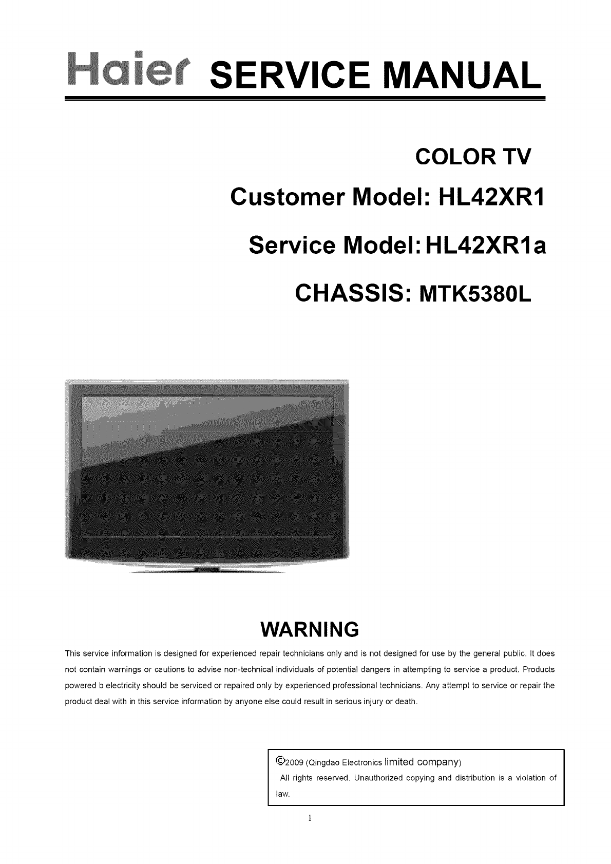
MSERVICE MANUAL
COLOR TV
Customer Model: HL42XR1
Service Model: HL42XR1a
CHASSIS: MTK5380L
WARNING
This service information is designed for experienced repair technicians only and is not designed for use by the general public. It does
not contain warnings or cautions to advise non-technical individuals of potential dangers in attempting to service a product. Products
powered b electricity should be serviced or repaired only by experienced professional technicians. Any attempt to service or repair the
product deal with in this service information by anyone else could result in serious injury or death.
_#2009 (Qingdao Electronics limited company)
All rights reserved. Unauthorized copying and distribution is a violation of
law.
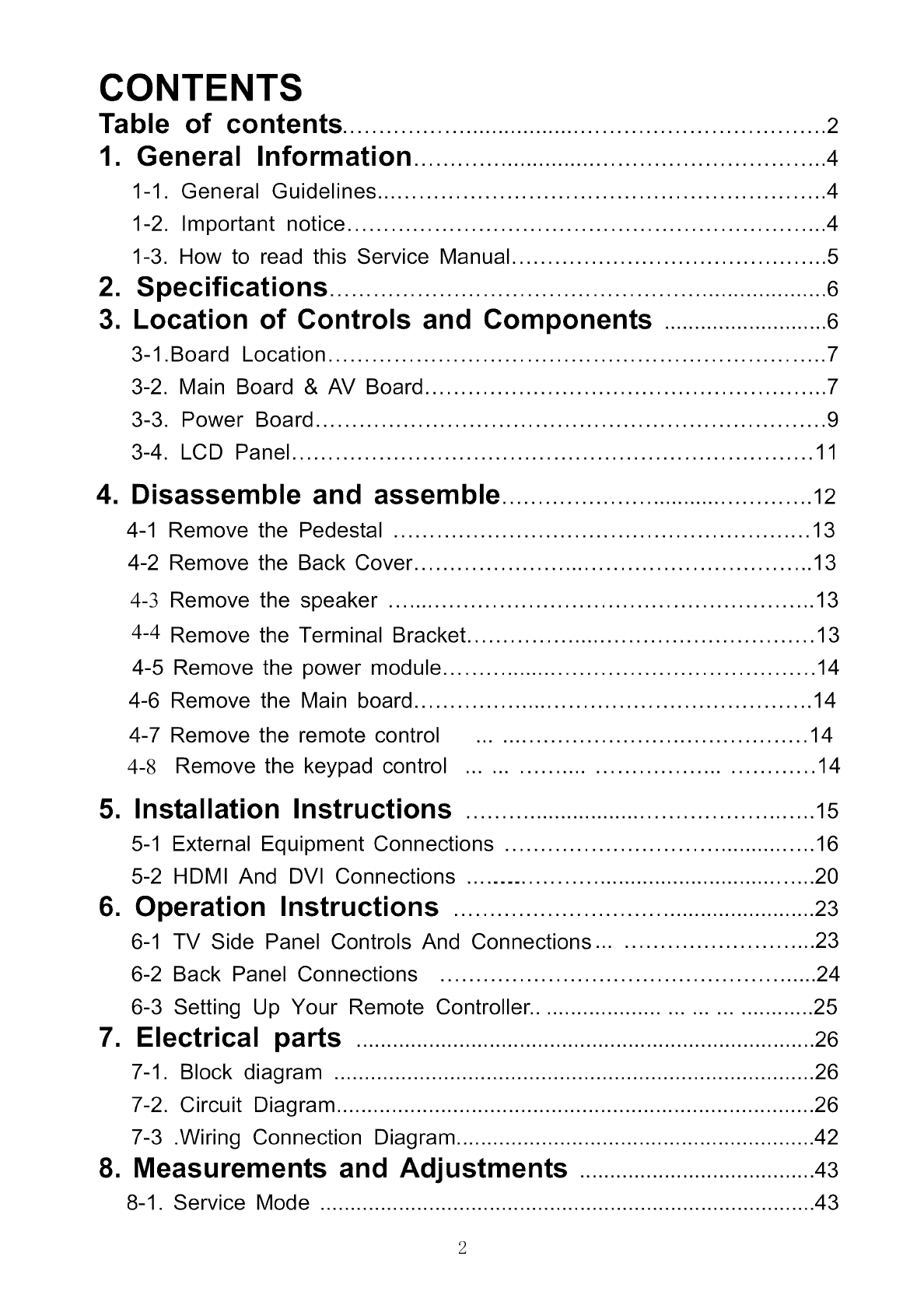
CONTENTS
Table of contents ..................................................................... 2
1. General Information ........................................................... 4
1-1. General Guidelines .............................................................. 4
1-2. Important notice .................................................................. 4
1-3. How to read this Service Manual ............................................ 5
2. Specifications ....................................................................... 6
3. Location of Controls and Components ...........................6
3-1.Board Location .................................................................... 7
3-2. Main Board & AV Board ........................................................ 7
3-3. Power Board ...................................................................... 9
3-4. LCD Panel ........................................................................ 11
4. Disassemble and
4-1 Remove the
4-2 Remove the
4-3 Remove the
4-4 Remove the
4-5 Remove the
4-6 Remove the
4-7 Remove the
assemble .............................................12
Pedestal .......................................................... 13
Back Cover ........................................................ 13
speaker ............................................................ 13
Terminal Bracket ................................................. 13
power module ..................................................... 14
Main board ........................................................ 14
remote control .............................................. 14
.............................................. 14
4-8 Remove the keypad control
Installation Instructions5 ..................................................... 15
5-1 External Equipment Connections ............................................. 16
5-2 HDMI And DVI Connections ...................................................... 20
6. Operation Instructions ...................................................... 23
6-1 TV Side Panel Controls And Connections .............................. 23
6-2 Back Panel Connections ..................................................... 24
6-3 Setting Up Your Remote Controller .......................................... 25
7. Electrical parts ............................................................................26
7-1. Block diagram ............................................................................... 26
7-2. Circuit Diagram .............................................................................. 26
7-3 .Wiring Connection Diagram ........................................................... 42
8. Measurements and Adjustments .......................................43
8-1. Service Mode .................................................................................. 43
2
11
8-2. Measurements and Adjustments .................................................. 43
Trouble shooting ......................................................................49
9-1. Simple check ............................................................................... 49
9-2. Power Supply Board failure check .............................................. 49
9-3. Main board failure check .............................................................. 51
9-4. Pannel failure ............................................................................... 53
3
1. General Information
1-1 General Guidelines
When servicing, observe the original lead dress. If a short circuit is found, replace all parts which
have been overheated or damaged by the short circuit.
After servicing, see to it that all the protective devices such as insulation barriers, insulation papers
shields are properly installed.
After servicing, make the following leakage current checks to prevent the customer from being
exposed to shock hazards.
1) Leakage Current Cold Check
2) Leakage Current Hot Check
3)Prevention of Electro Static Discharge(ESD)to Electrostatically Sensitive
1-2 Important notice
1-2-1. Follow the regulations and warnings
Most important thing is to list up the potential hazard or risk for the service personnel to open the
units and disassemble the units. For example, we need to describe properly how to avoid the
possibility to get electrical shock from the live power supply or charged electrical parts (even the
power is off).
This symbol indicates that high voltage is present inside. It is dangerous to
make any king of contact with any inside part of this product.
This symbol indicates that there are important operating and maintenance
instructions in the literture accompanying the appliance
1-2-2. Be careful to the electrical shock
To prevent damage which might result in electric shock or fire, do not expose this TV set to rain or
excessive moisture. This TV must not be exposed to dripping or splashing water, and objects
Filled with liquid, such as vases, must not be place on top of or above the TV
1-2-3. Electro static discharge (ESD)
Some semiconductor (solid state) devices can be damaged easily by static electricity. Such
Components commonly are called Electrostatically Sensitive (ES) Devices. The following
tech-niquesshouldbeusedtohelpreducetheincidenceofcomponentdamagecausedbyelectro
Static discharge (ESD).
1-2-4. About lead free solder (PbF)
This product is manufactured using lead-free solder as a part of a movement within the consum-er
products industry at large to be environmentally responsible. Lead-free solder must be used in the
servicing and repair of this product.
1-2-5. Use the genewing parts (specified parts)
Special parts which have purposes of fire retardant (resistors),high-quality sound (capacitors), low
noise(resistors), etc. are used.
When replacing any of components, be sure to use only manufacture's specified parts shown in
the parts list.
Safety Component
• Components identified by mark have special characteristics important for safety.
4
1-2-6. Safety Check after Repairment
Confirm that the screws ,parts and wiring which were removed in order to service are put in the
original positions, or whether there are the portions which are deteriorated around the serviced
places serviced or not. Check the insulation between the antenna terminal or external metal and
the AC cord plug blades. And be sure the safety of that.
Insuration Test
1. Unplug the plug from the AC outlet.
2. Remove the antenna terminal on TV and turn on the TV.
3. Insulation resistance between the cord plug terminals and the eternal exposure metal
should be more than M ohm by using the 500V insulation resistance meter
4. If the insulation resistance is less than M ohm, the inspection repair should be required.
If you have not the 500V insulation resistance meter, use a Tester.
External exposure metal: Antenna terminal Headphone jack
1-2-7. Ordering Spare Parts
Please include the following informations when you order parts. (Particularly the Version
letter)
1. Model number and Version letter
The model number can be found on the back of each product and the Version letter can
be found at the end of the serial number.
2. Part No. and Description
You can find them in your service manual
1-2-8. Photo used in this manual
The illustration and photos used in this Manual may not base on the final design of products, which
may differ from your products in some way.
1-3. How to read this Service Manual
1-4-1. Using Icons
Icons are used to attract the attention of the reader to specific information. The meaning of each icon is
described in the table below:
Note:
A "note" provides information that is not indispensable, but may nevertheless be valuable to the
reader, such as tips and tricks.
Caution:
A "caution" is used when there is danger that the reader, through incorrect manipulation,
5
maydamageequipment,loosedata,get anunexpectedresultor hasto restart(partof)
a procedure.
Warning:
A "warning"is usedwhenthereis dangerof personalinjury.
R ce:
A "reference"guidesthe readerto otherplacesinthis binderor in this manual,wherehe/shewill
findadditionalinformationona specifictopic.
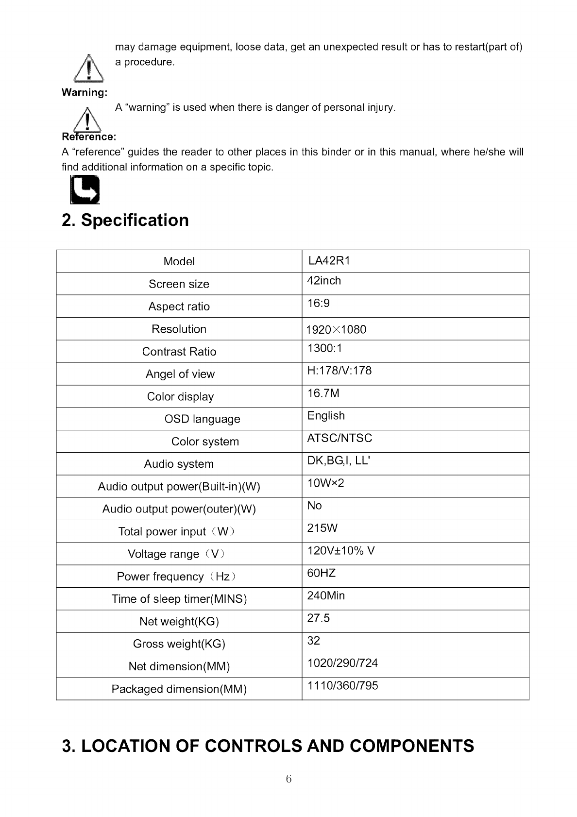
2. Specification
Model LA42R1
Screen size 42inch
Aspect ratio 16:9
Resolution 1920×1080
Contrast Ratio 1300:1
Angel of view H: 178/V: 178
Color display 16.7M
OSD language English
Color system ATSC/NTSC
Audio system DK,BG, I, LL'
Audio output power(Built-in)(W) 10Wx2
Audio output power(outer)(W) No
Total power input (W) 215W
Voltage range (V) 120V+10% V
Power frequency (Hz) 60HZ
Time of sleep timer(MINS) 240Min
Net weight(KG) 27.5
Gross weight(KG) 32
Net dimension(MM) 1020/290/724
Packaged dimension(MM) 1110/360/795
3. LOCATION OF CONTROLS AND COMPONENTS
6
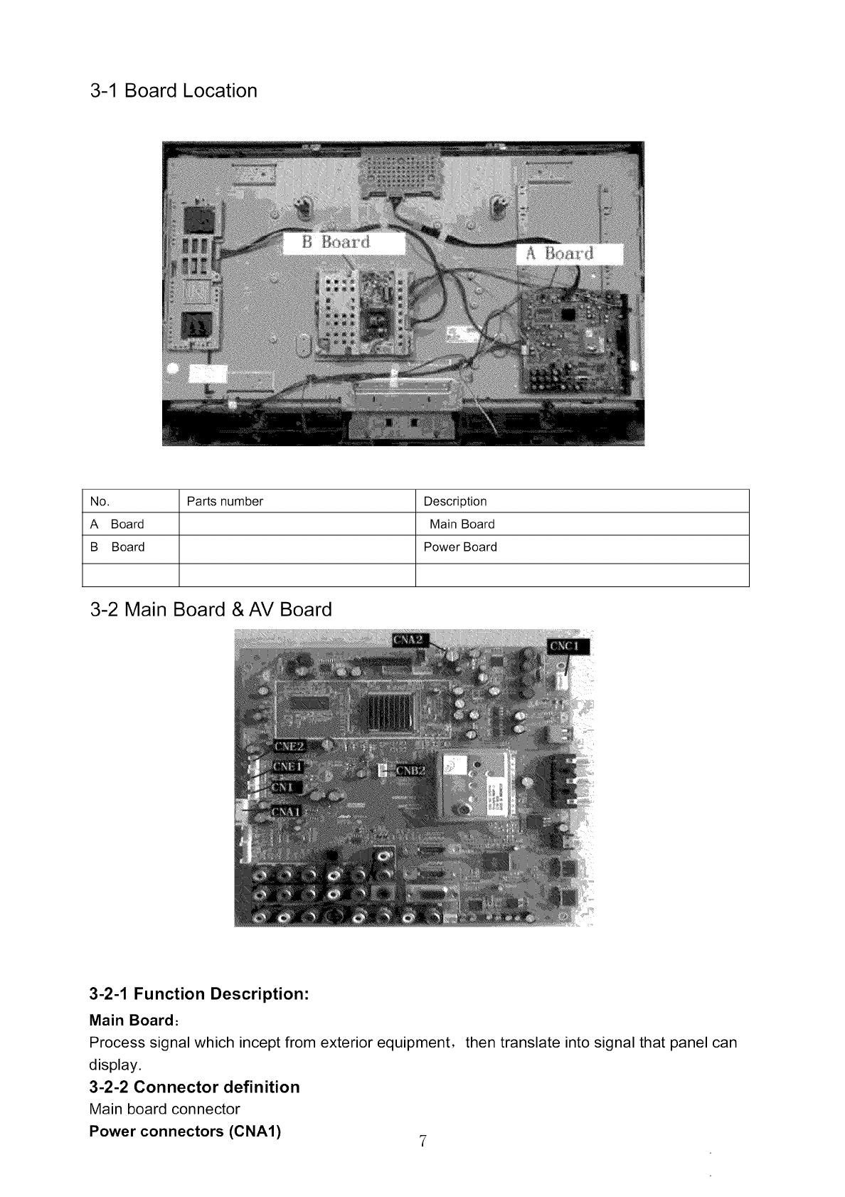
3-1 Board Location
No. Parts number Description
A Board Main Board
B Board Power Board
3-2 Main Board & AV Board
3-2-1 Function Description:
Main Board:
Process signal which incept from exterior equipment, then translate into signal that panel can
display.
3-2-2 Connector definition
Main board connector
Power connectors (CNA1) 7
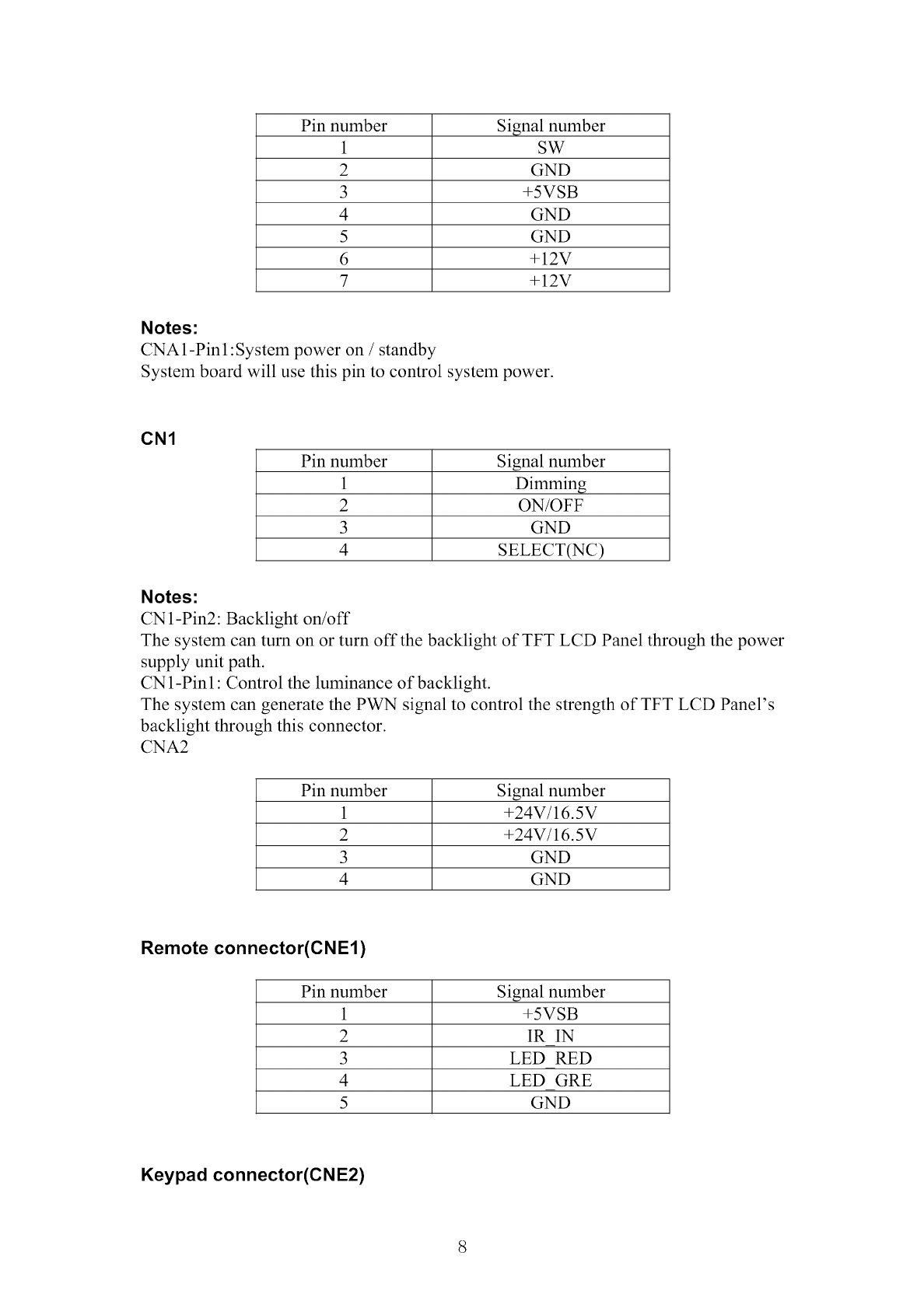
Pin number
1
2
3
4
5
6
7
Signal number
SW
GND
+5VSB
GND
GND
+12V
+12V
Notes"
CNA 1-Pin 1:System power on /standby
System board will use this pin to control system power.
CN1
Pin number
1
2
3
4
Signal number
Dimming
ON/OFF
GND
SELECT(NC)
Notes:
CN 1-Pin2: Backlight on/off
The system can turn on or turn off the backlight of TFT LCD Panel through the power
supply unit path.
CN 1-Pinl: Control the luminance of backlight.
The system can generate the PWN signal to control the strength of TFT LCD Panel's
backlight through this connector.
CNA2
Pin number Signal number
1 +24V/16.5V
2 +24V/16.5V
3 GND
4 GND
Remote connector(CNE1)
Pin number Signal number
1 +5VSB
2 IR IN
3 LED RED
4 LED GRE
5 GND
Keypad connector(C NE2)
8
Pin number
1
2
3
Signal number
GND
ADIN l-K0
ADIN2-K1
Speaker connector(CNC1)
Pin number
1
2
3
4
Signal number
SPEA L+
SPEA L-
SPEA R
SPEA R+
Other con nectors:
CNB2 to Upgrade the program of MTK5380L (U13) AND FLASH (U17)
J3
+3V3SB 1 D
UORX 2
UOTX 3
4
4xl WIHOUSnNG
DIP41W/HIP2_O
3-3. Power Board
3-3-1 Function Description:
Supply power for Main board, Panel.
3-3-2Connectordefinition
CON3
9
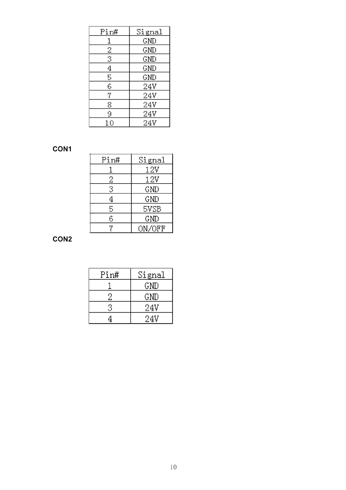
Pin# Signal
1 GND
GND
GND
4 GND
5 GND
6 24V
7 24V
8 24V
9 24V
i0 24V
Pin# Si_nal
12V
2 12V
3 GND
4 6ND
5 5VSB
6OI_
7 ON/OFF
CON1
CON2
Pin#
1
2
4
Signal
6ND
24V
24V
IO
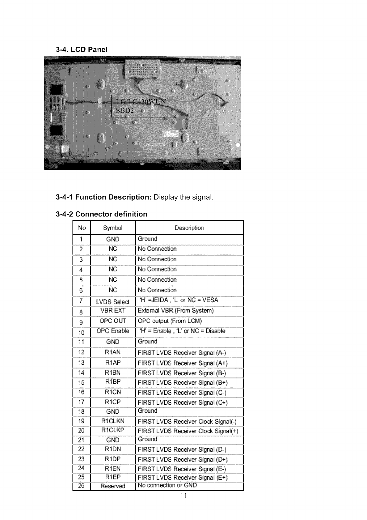
3-4. LCD Panel
3-4-1 Function Description: Display the signal.
3-4-2 Connector definition
No S_I Descd_ion
'1 GND Gr,au_
2 NC No Conn_tign
3 NC No Conn_tien
4 NC
5 NC
8 VBR EXT
9 OPC O_
11 GND
No :Conn_tion
No ConneXion
No ConneXion
Ex_mal VBR (From System)
OPC ou_ (From LCIVI)
G;rou_
t2 R1AN F_RST LVDS R_eiver Sig_;l (A-)
14 R1BN FIRST LVDS R_eiver Sig_l (B-)
15 R1BP F_RS]°LVDS R_eiver Sig_l (B+)
1,6 R1CN FIRST LVDS R_eiver Sig_l (_)
17 RtCP HRST LVDS R_eiver Signal (C+)
19 R1CLKN HRST LVDS R_:eiver Clock Si9_l(- )
11

No
Bit Sel_t 'H' or NC= 10bit(D)_ 'L' = 8bit
28 _AN SECOND LVDS R_eiver Sig_l (A-)
SECOND LVDS R_eiver S,ig_l (A+)
................... ; ; ; ........................ ; ; <;; ; ............................................................
SECON D LVDS R_eiver Sigral (B-)
3'I SECOND LVDS Receiver Sigral (B+)
32 R2CN SECOND LVDS R_eiver Sig_l (C-)
SECOND LVDS R_eiver Sig_l (C÷)
34 GND Ground
....................... ............................ ......................................; ,;; ; ...............................;; ; ; <; ;..............
SECOND LVDS R_eiver Cl_k Signal(-)
SECOND LVDS R_eiver Cl_k Signal(+)
37 GND Ground
SECON D LVDS R_eiver Sig_l (_)
SECON D LVDS R_eiver Sig_l (D+)
........................... ......................................... ............................................. <; .......................................................
SECOND LVDS R_eiver Sig_l (E-)
41 SECON D LVDS Receiver Sigr_l (E÷)
................42 i,on,orGND..........................................................................................................................................................................................................................
4:3 Resew_ t'1oconr_ion or GND
44 GND
i • i
45 GND Ground
46 GND Ground
48 VLCD Po'_r Sup#y +i2_0V
4.Disassemble and assemble
12
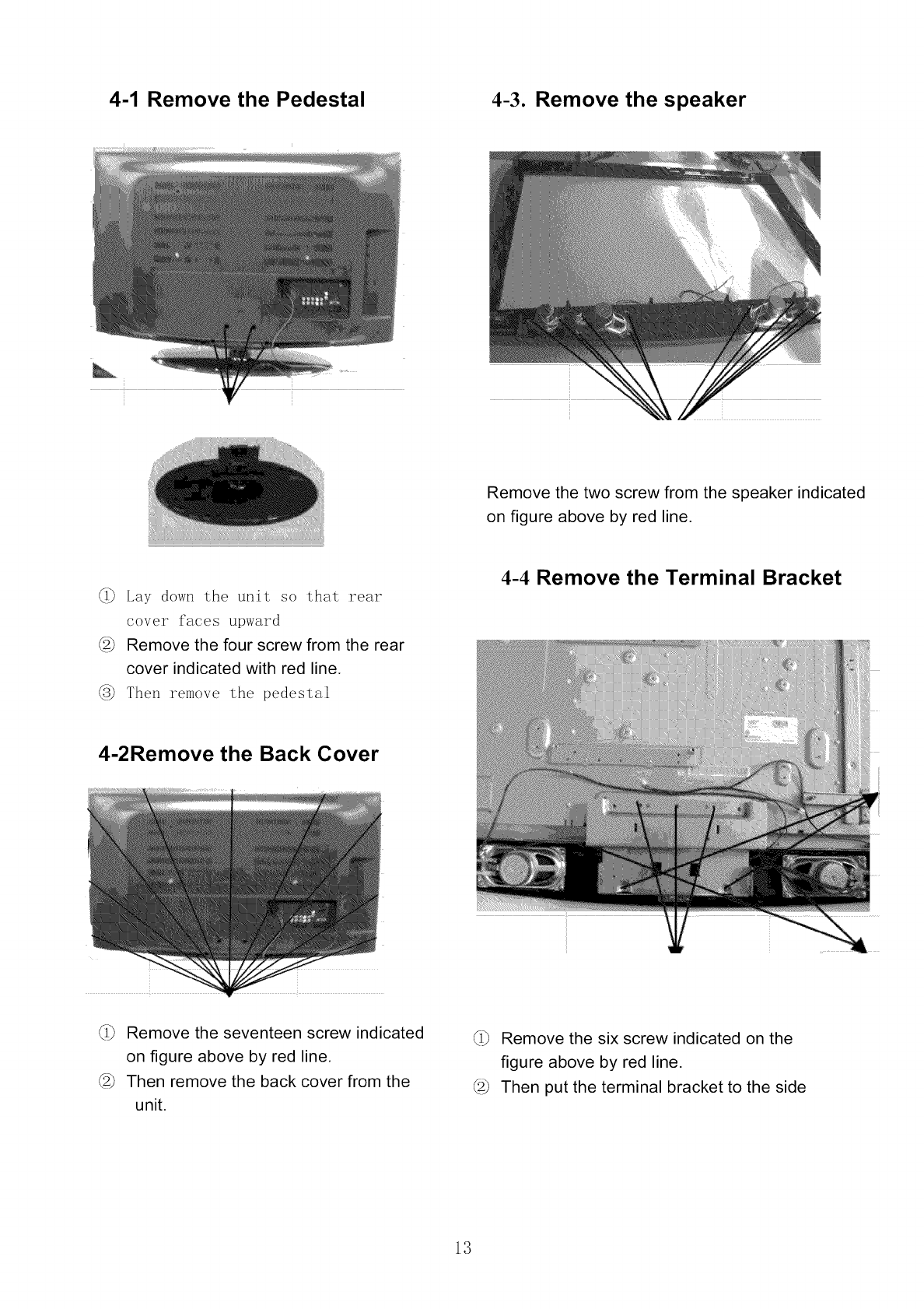
4-1 Remove the Pedestal 4-3. Remove the speaker
Remove the two screw from the speaker indicated
on figure above by red line.
(]) [Jay down the unit so that rear
cover faces upward
(2) Remove the four screw from the rear
cover indicated with red line.
_3) Then remove the pedestal
4-4 Remove the Terminal Bracket
4-2Remove the Back Cover
(1) Remove the seventeen screw indicated
on figure above by red line.
(2) Then remove the back cover from the
unit.
(`1) Remove the six screw indicated on the
figure above by red line.
(2) Then put the terminal bracket to the side
13

4-5 Remove the power module 4-8 Remove the keypad control
_1_ Remove the four screw indicated on the
figure above by the red line.
_2_ Then remove the power module
4-6 Remove the Main board [] Remove the two screw indicated on the figure
above by blue line.
_Then remove the keypad module.
_1_ Remove the eight screw indicated on the
figure above by the red line.
_2_Remove the Main board
4-7 Remove the remote control
Remove the one screw, take out the remote
control board
14
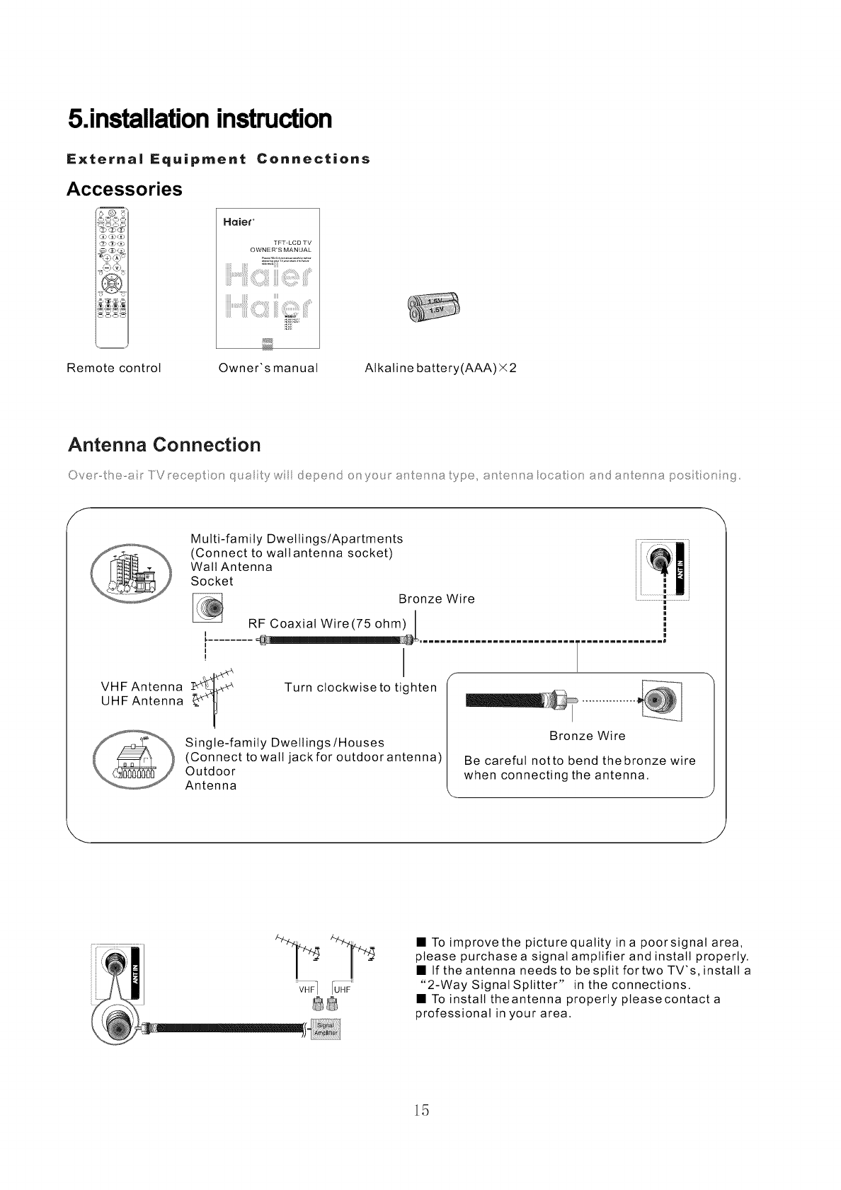
5.installationinstruction
Externa| Equipment Connections
Accessories
Haie¢ o
TFT-LCD TV
OWNER'S MANUAL
7
Remote control Owner's manual Alkaline battery(AAA) X 2
Antenna Connection
VHF Antenna
UHF Antenna
Single-family Dwellings/Houses
(Connect to wall jack for outdoor antenna)
Outdoor
Antenna
Multi-family Dwellings/Apartments
(Connect to wallantenna socket)
Walt Antenna
Socket
Bronze Wire ,................................................
,
RF Coaxial Wire(75 ohm) I
i........ _ _ ........................... ,-.............. ;
i, /
Turn ctockwiseto tighten _ ................
Bronze Wire
Be careful notto bend thebronze wire
when connecting the antenna•
-p-p
'v.--qF_
88
• To improve the picture quality in a poorsignal area,
please purchase a signal amplifier and install properly•
• If the antenna needs to be split fortwo TV's, install a
"2-Way Signal Splitter" in the connections•
• To install theantenna properly pteasecontact a
professional in your area.
15
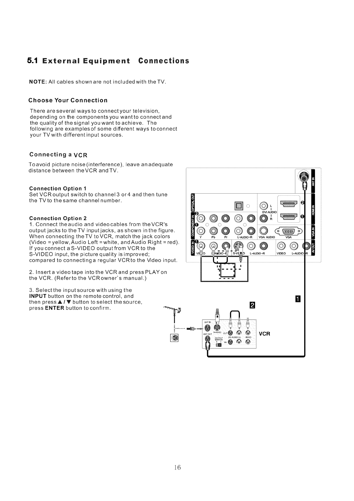
5.1 External Equipment Connections
NOTE: All cables shownare not included with theTV.
Choose Your Connection
There are several ways to connectyour television,
depending on the components you wantto connectand
the quality of the signal you want to achieve. The
following are examplesof some different ways toconnect
your TVwith differentinput sources.
Connecting aVCR
Toavoid picture noise(interference), leave anadequate
distance between theVCR and TV.
Connection Option 1
Set VCRoutput switch to channel3 or4 and then tune
the TVto the same channel number.
Connection Option 2
1. Connect theaudio and videocabtes from theVCR's
output jacks to theTV input jacks, as shown in the figure.
When connecting theTV toVCR, match the jack colors
(Video =yellow,Audio Left =white, andAudio Right =red).
If you connect a S-VIDEO outputfrom VCRto the
S-VIDEO input, the picture quality is improved;
compared to connectinga regular VCRto the Video input.
2. Inserta video tape into the VCRand press PLAY on
the VCR. (Referto the VCRowner's manual.)
@@
O Q
0@
Y Pb Pr
@ @ DV,AUD,O
©"@',o
L-AUDIO-R VGA AUDIO VGA
@@ @@
L-AUDIO -R JVIDEO L-AUDIw
3. Setect the inputsource with using the
INPUT button on the remote control, and
then pressA/V button to select the source,
press ENTER button to confirm.
n
[]
i....... VCR
16
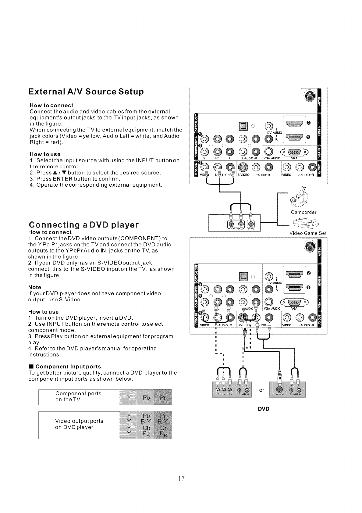
External A/V Source Setup
How to connect
Connect the audio and video cables from the external
equipment's output jacks to the TVinput jacks, as shown
in the figure.
When connecting the TVto external equipment, match the
jack colors (Video =yellow, Audio Left =white, and Audio
Right =red).
How to use
1. Selectthe input source with using the INPUT button on
the remote control.
2. Press A/Y button to select the desired source.
3. Press ENTER button to confirm.
4. Operate thecorresponding external equipment.
Connecting a DVD player
How to connect
1. Connect the DVD video outputs(COMPONENT) to
the YPb Prjacks on the TVand connect the DVDaudio
outputs tothe YPbPrAudio IN jacks onthe TV, as
shown in the figure.
2. If your DVD onlyhas an S-VlDEOoutput jack,
connect this to the S-VIDEO inputon theTV, as shown
in the figure.
Note
If yourDVD player does not have componentvideo
output, use S-Video.
How to use
1. Turn on the DVD player, insert a DVD.
2. Use INPUTbutton on theremote control tosetect
component mode.
3. Press Play button on external equipment forprogram
play.
4. Referto the DVD player's manual foroperating
instructions.
• Component Inputports
To get better picture quality, connect a DVD ptayerto the
component input ports as shown below.
Component ports
on the TV
Video output ports
on DVD player
DVI AUDIO
©@©@@'.
© () ©
@@@@@
Pb Pr L-AUD!O-R i VGA AUDIO
S-VIDEOL-AUDIO-R
VGA
©©@
VIDEO L-AUDIO -R
F _/trder
Video Game Set
@@
© ©
DVI AUDIO
#©
[ VGA AUDIO
or
V_
@@@
VIDEO L-AUDIO -R
DVD
17
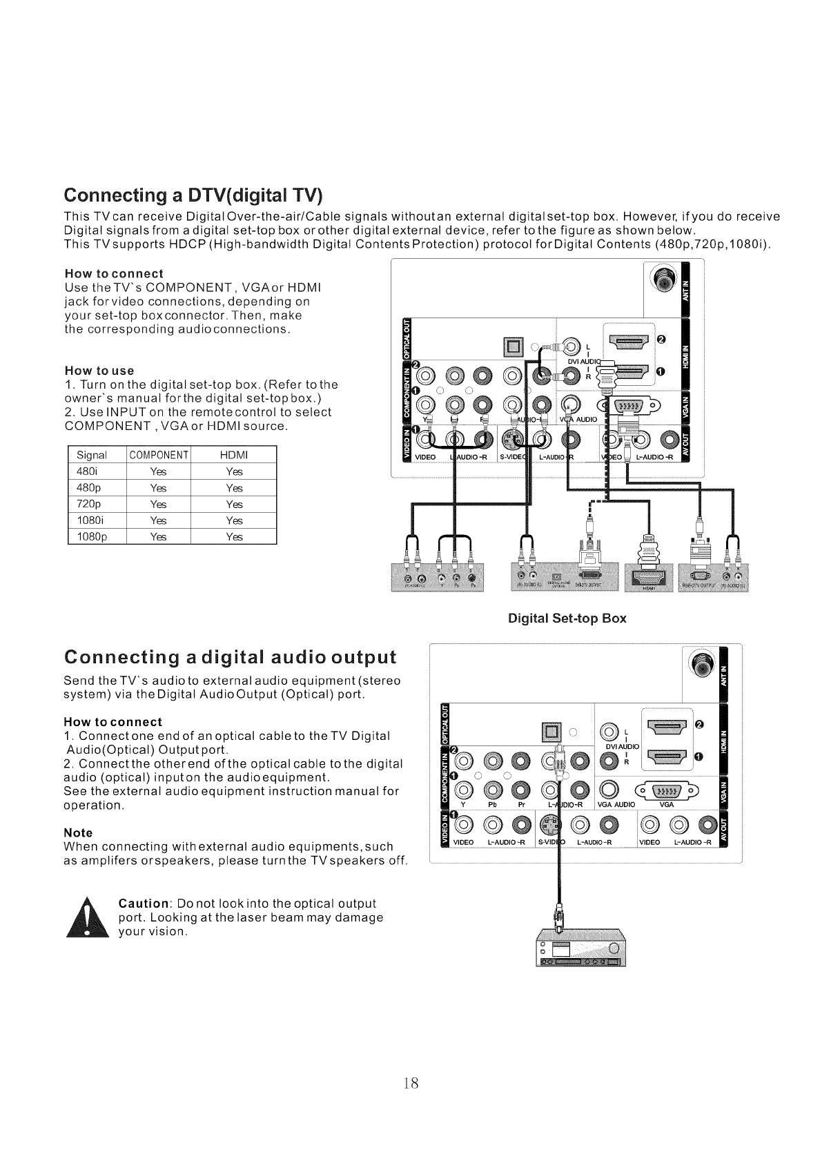
Connecting a DTV(digitai TV)
This TV can receive Digital Over-the-air/Cable signals withoutan external digital set-top box. However, if you do receive
Digital signals from adigital set-top box or other digital external device, refer to the figure as shown below.
This TVsupports HDCP (High-bandwidth Digital Contents Protection) protocol forDigital Contents 480p,720p,1080i).
How to connect
Use theTV's COMPONENT, VGAor HDMI
jack forvideo connections, depending on
your set-top boxconnector. Then, make
the corresponding audioconnections.
How to use
1. Turn on the digital set-top box. (Refer to the
owner's manual forthe digital set-topbox.)
2. Use INPUT on the remote control to select
COMPONENT ,VGAor HDMI source.
Signal COMPONENT HDMi
480i Yes Yes
480p Yes Yes
720p Yes Yes
1080i Yes Yes
1080p Yes Yes
@@@
0
Digital Set=top Box
Connecting a digital audio output
Send theTV's audio to external audio equipment (stereo
system) via the Digital Audio Output (Optical) port.
How to connect
1. Connect one end of an optical cable to theTV Digital
Audio(Optical) Output port.
2. Connect the otherend of the optical cable tothe digital
audio (optical) inputon the audioequipment.
See the external audio equipment instruction manual for
operation.
Note
When connecting with external audio equipments,such
as amptifers orspeakers, please turnthe TVspeakers off.
Caution: Do not look into the optical output
port. Looking at the laser beam may damage
your vision.
@@
© ©
@@
YPb Pr
©@
VIDEO L-AUDIO °R
©
i VGA AUDIO VGA
@@ @@@
L-AUDIO -R VIDEO L-AUDIO _R
18
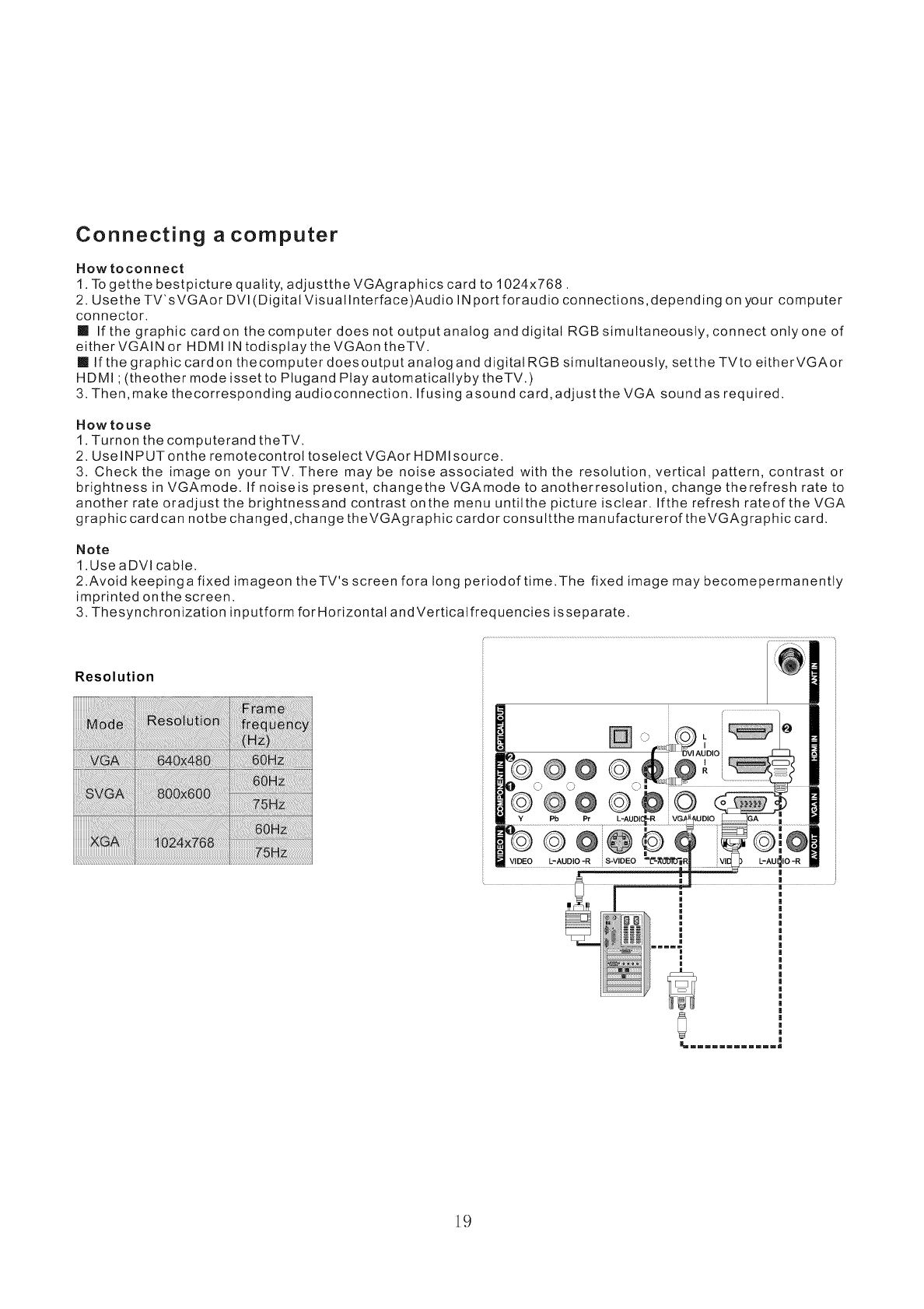
Connecting acomputer
Howtoconnect
1. To getthe bestpicture quality, adjustthe VGAgraphics card to 1024x768.
2. Usethe TV'sVGAor DVI (Digital Visuallnterface)Audio IN port foraudio connections,depending on your computer
connector.
[] If the graphic card on the computer does not output analog and digital RGBsimultaneously, connect only one of
eitherVGAIN or HDMI IN todisplaytheVGAon theTV.
[] If the graphic card on thecomputer doesoutput analog and digitaIRGB simultaneously, setthe TVto eitherVGAor
H D M I ; (theother mode isset to Plugand Play automaticatlyby theTV.)
3. Then,make thecorresponding audioconnection. Ifusing asound card,adjust the VGA sound as required.
Howtouse
1. Turnon thecomputerand theTV.
2. UselNPUTonthe remotecontrottoselectVGAor HDMIsource.
3. Check the image on your TV. There may be noise associated with the resolution, vertical pattern, contrast or
brightness in VGAmode. If noiseis present, changethe VGAmode to anotherresotution, change therefresh rate to
another rate oradjust the brightnessand contrast onthe menu untilthe picture isclear. Ifthe refresh rateof the VGA
graphiccardcan notbe changed,changetheVGAgraphiccardor consultthe manufactureroftheVGAgraphiccard.
Note
1.UseaDVl cable.
2.Avoid keepinga fixed imageon theTV's screen fora long periodof time.The fixed image may becomepermanently
imprinted onthescreen.
3. Thesynchronization inputform for Horizontal andVerticatfrequencies isseparate.
Resolution
VIDEO
@@@
Q Q
©@©
Pb Pr
© @@
L-AUDIO-R ::S-VIDEO
L
I
_mmmmmmmmmmmml
19
5.2 HDNll and DVI Connection
When thesource device(DVD player or SetTop Box) supports HDMI
How To Connect
1. Connect thesource device toHDMI portof thisTV withan HDMI cable(notsupplied with thisproduct).
2. No separatedaudio connection is necessary.
How To Use
If the source device supports Auto HDMI function, the output resolution of the source device will be automatically
set to 1280x720p.
If the source device does not supportAuto HDMI, you need to set the output resolution appropriately.
To get the best picture quatity, adjust the output resolution of the source device to 1280x720p.
Select HDMI input source in inputsource option of Select Main source menu.
When the source device(DVD playeror Set Top Box) supports DVl
How To Connect
1. Connect thesource device toHDMI portof this TV witha HDMI-to-DVI cable(not supplied withthis product).
2. Aseparated audio connection is necessary.
3. If the source device hasan analog audio output connector, connect the source device audio output to DVlAudio
In port Iocatedon the leftside of HDMI port.
How To Use
If the source device supports Auto DVl function, the output resolution of the source device wilt be automatically
set to 1280x720p.
If the source device does notsupportAuto DVl, you need to set the output resolution appropriately.
To get the best picture quality, adjust the output resolution of the source device to 1280x720p.
Press the INPUT button to select HDMI inputsource in input source option of Select Main source menu.
2O
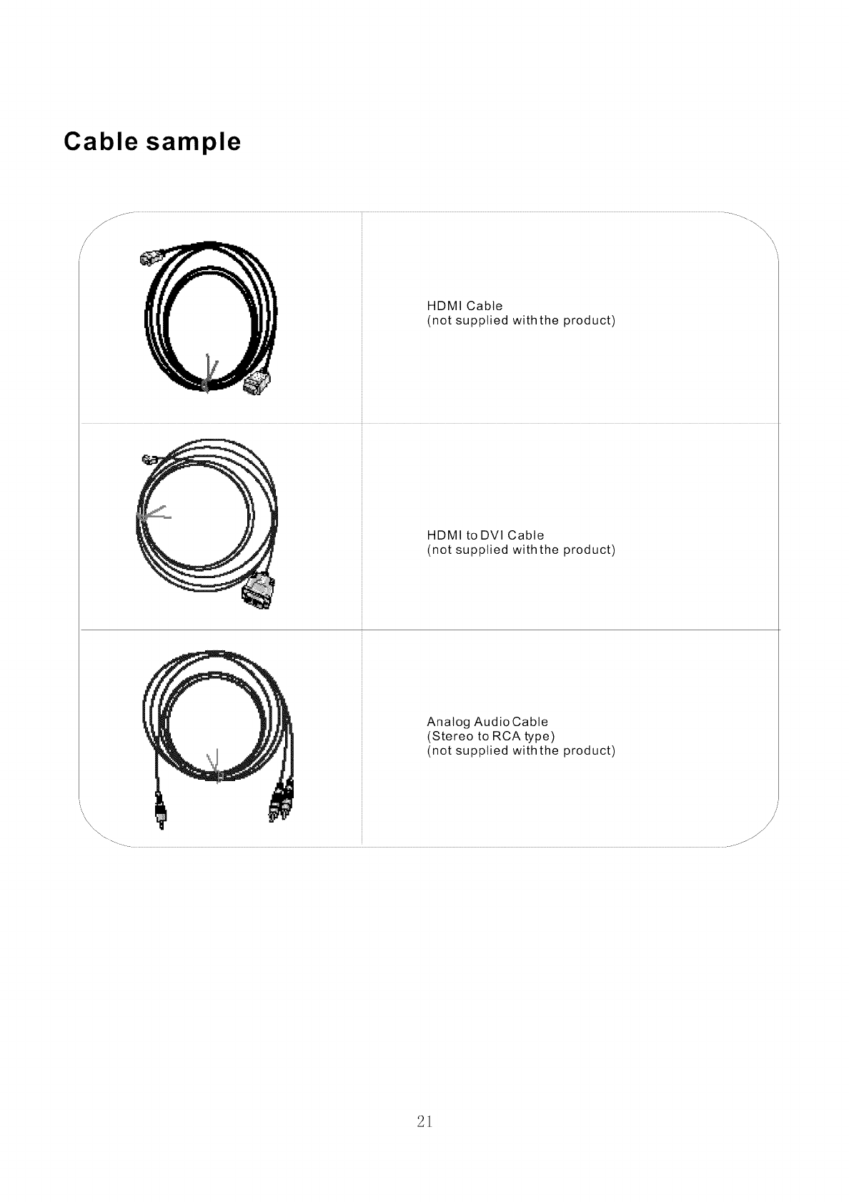
Cable sample
\
HDMI Cable
(not supplied withthe product)
HDMI to DVl Cable
(not supplied withthe product)
Analog Audio Cabte
(Stereo to RCA type)
(not supplied withthe product)
"\\\\\
21
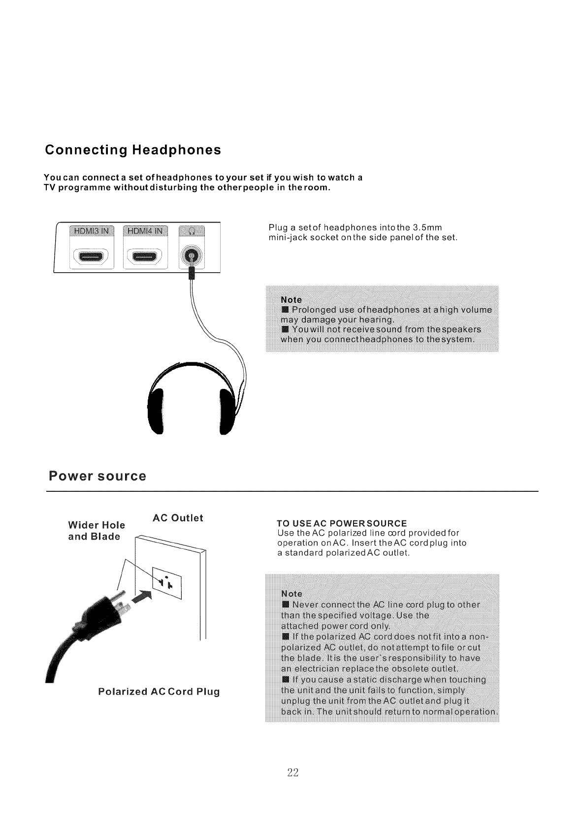
Connecting Headphones
You can connecta set of headphones to your set if you wish to watch a
TV programme withoutdisturbing the otherpeople in theroom.
Plug a setof headphones intothe 3.5mm
mini-jack socket onthe side panelof the set.
Power source
Wider Hole
and Blade
AC Outlet TO USEACPOWERSOURCE
Use theAC polarized line cord provided for
operation onAC, Insert theAC cord plug into
a standard potarizedAC outlet.
Polarized AC Cord Plug
22
6. Operation Instructions
Basal information
iI_' ):;;! 'q
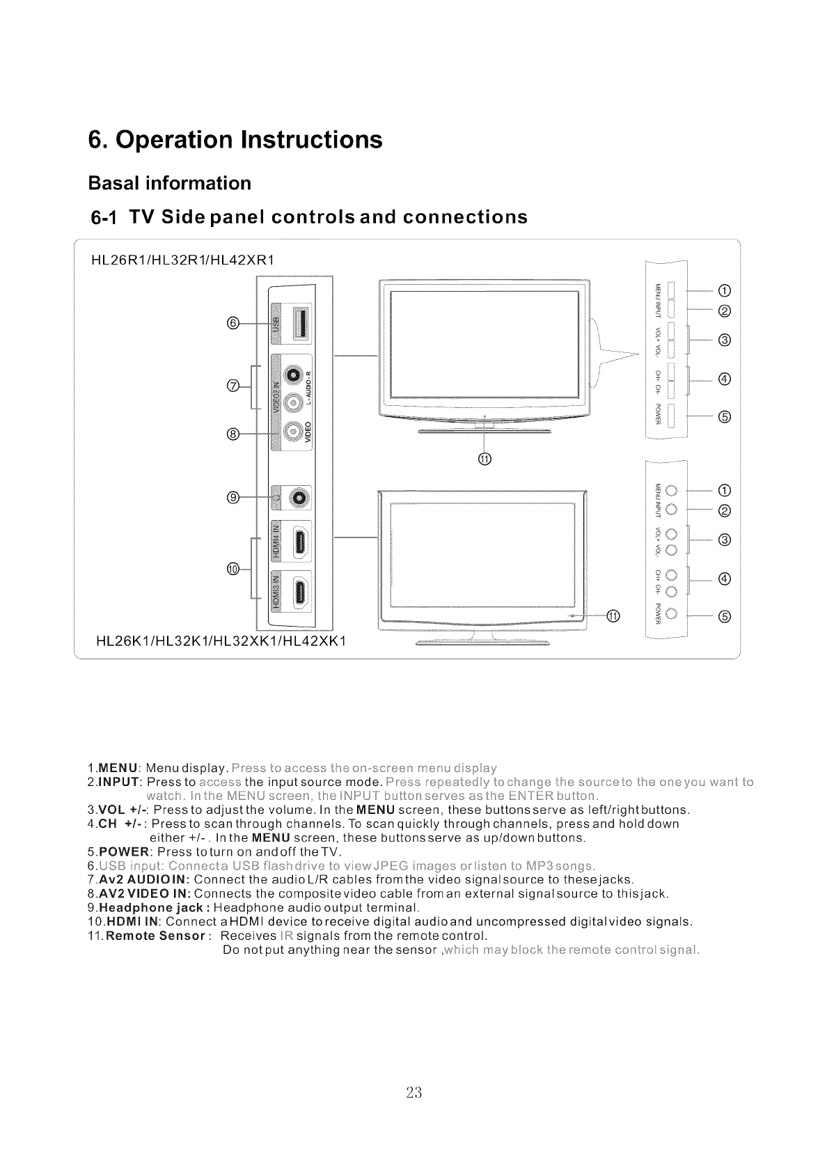
HL26K1/HL32K1/HL32XK1/HL42XK1
®
i iili....................®
i-¸ •........... i
/................1@
i o
_- _.¢' ..............
<f-_,
o\j
r-
2 y >' i
+\/ ......................(_)
2 s_
, \/
1.MENU: Menu display. Press oaccess heo_-scF-eer r_erudspay
2.iNPUT: Press to _ccess the input source mode. Pressrepe;:4edytoc}a_gethesouF-ceo/eo_eyouwsFt o
wach. he MENUscF-eeF he NPU/butor se_vesas _eEN_F[_ilRb tot.
3.VOL +/< Press to adjust the volume. In the MENU screen, these buttons serve as left/rightbuttons.
4.CH +/-: Press to scan through channels. To scan quickly through channels, press and hold down
either +/-. In the MENU screen, these buttonsserve as up/downbuttons.
5.POWER: Press toturn on andoff theTV.
6.USB rput:Cor_eca USBfas} drve ovewJPEG m_gesor ste_ o MP3sorgs,
7.Av2 AUDIOJN: Connect the audio L/R cables fromthe video signalsource to these jacks.
8.AV2WDEO iN: Connects the compositevideo cable froman external signalsource to this jack.
9.Headphone jack :Headphone audio output terminal.
10.HDM! IN: Connect aHDMI device toreceive digital audioand uncompressed digitalvideo signals.
11. Remote Sensor : Receives R signals from the remote control.
Do not put anything near the sensor,whch _/sybeck here_otec rtro s_8
23
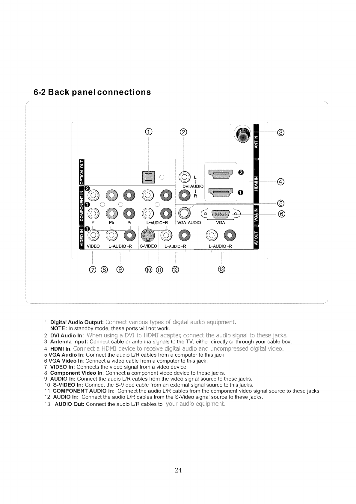
6-2 Back panel connections
©
Pb Pr
i
L-AUDIO -R S-VIDEO
®
L i°
I
DVI AUDIO
/
L-AUDIO -R
@
VGA AUDIO VGA
@
L-AUDIO -R
o@ @ oo o
®
®
®
@
1. Digital Audio Output: Connect: vat ous Iypes of d gil:;}_t_}_tsdo equ pment
NOTE: In standby mode, these ports will not work.
2. DVI Audio In: When us_9 a DVZ to HDe_Z adapter_ conned: the audo sDnat to these ;scks
3. Antenna Input: Connect cable or antenna signals to the TV, either directly or through your cable box.
4. HDMI In: Co nect a HDF_I dc_vce to rece w_ dgb2t audo and uncompressed d _ t_ vdeo
5.VGA Audio In: Connect the audio L/R cables from a computer to this jack.
6.VGA Video In: Connect a video cable from a computer to this jack.
7. VIDEO In: Connects the video signal from a video device.
8. Component Video In: Connect a component video device to these jacks.
9. AUDIO In: Connect the audio L/R cables from the video signal source to these jacks.
10. S-VIDEO In: Connect the S-Video cable from an external signal source to this jacks.
11. COMPONENT AUDIO In: Connect the audio L/R cables from the component video signal source to these jacks.
12. AUDIO In: Connect the audio L/R cables from the S-Video signal source to these jacks.
13. AUDIO Out: Connect the audio L/R cables to yor ado equipment
24
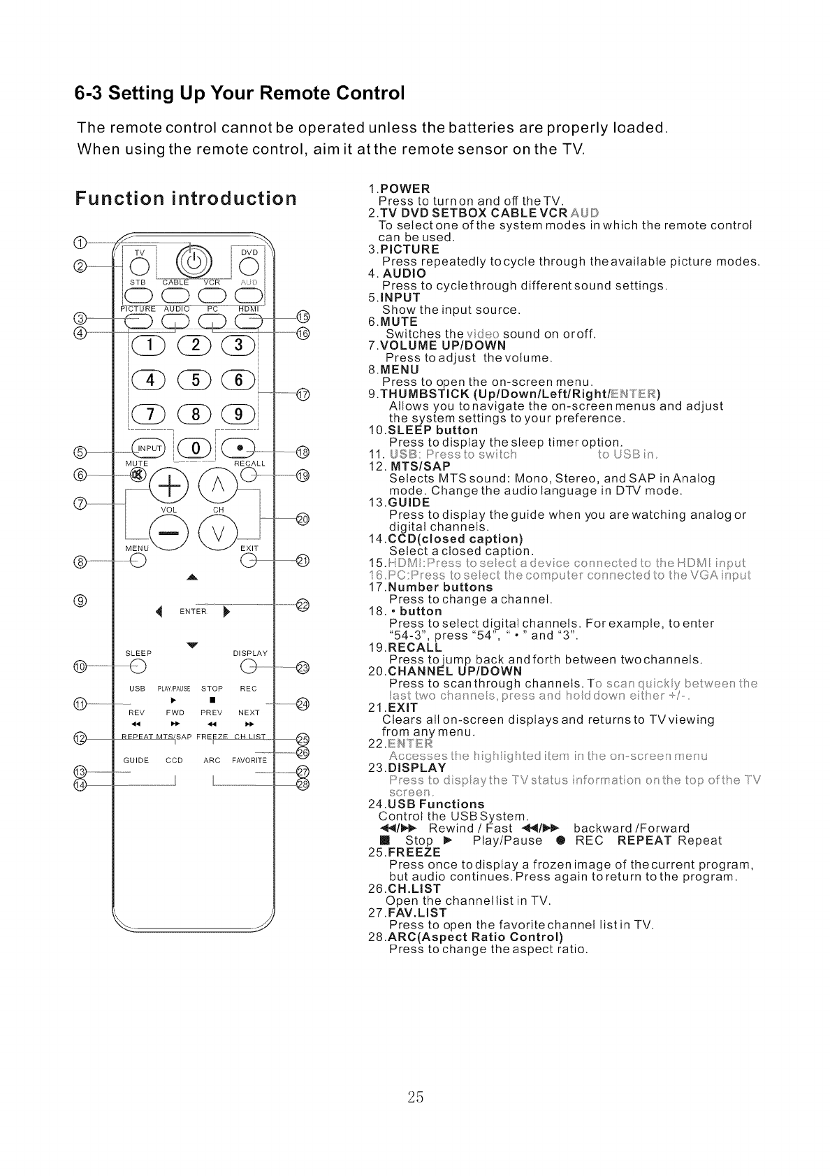
6-3 Setting Up Your Remote Control
The remote control cannot be operated unless the batteries are properly loaded.
When using the remote control, aim it atthe remote sensor on the TV.
Function introduction
O ...........
@
Q .....
@--
ENTER
V
SLEEP DISPLAY
USB PLAY/PAUSE STOP REC
REV FWD PREV NEXT
__REPEAI MTS/_SAP FRE_£ CHL/SI
GUIDE CCD ARC FAVORITE
........
.... O
......... O
...........................
--@
....... Q
1 .POWER
Press to turnon and off theTV.
2.TV DVD SETBOX CABLEVCRAUD
To select one ofthe system modes in which the remote control
can be used.
3.PICTURE
Press repeatedly tocycle through theavailabte picture modes.
4. AUDIO
Press to cyctethrough differentsound settings.
5.INPUT
Show the input source.
6.MUTE
Switches the v eosoundonoroff.
7.VOLUME UP/DOWN
Press toadjust thevolume.
8.MENU
Press to open the on-screen menu.
9.THUMBSTICK (UplDownlLeftlRightlENT_£R)
Allows you to navigate the on-screen menus and adjust
the system settings to your preference.
10.SLEEP button
Press to display the sleep timer option.
11. USB:Press o sw ch oUSB r,
12. MTS/SAP
Selects MTSsound: Mono, Stereo, and SAP in Analog
mode. Change the audio language in DTV mode.
13.GUIDE
Press to display the guide when you are watching analog or
digital channels,
14.CCD(closed caption)
Select a closed caption.
15./4DM:Presstoseect_de*, cecor/ectedto_he/4DM rput
16PC:PFess oseect hece_putercor_eced o heVGA rput
17.Number buttons
Press to change a channel.
18. •button
Press to select digital channels. For example, to enter
"54-3", press "54", " o " and "3".
19.RECALL
Press to jump back andforth between twochannels.
20.CHANNEL UP/DOWN
Press to scanthrough channels. To sc_ qucky beweer he
as_. wochs_es p_essa_dtoddowr_e let _/_
21 .EXIT
Clears all on-screen displays and returns to TVviewing
from any menu.
22._!f:N7 F!.R
Accesses hehgh ghted tern r theo_sc_eer _eru
23.DISPLAY
Press_odspsy h_ lVsatus rfo__ato_ o_ he opofhe IV
SO eof _
24.USB Functions
Control the USBSystem.
_1/_ Rewind /Fast 4_11/_ backward/Forward
[] Stop D,, Play/Pause • REC REPEAT Repeat
25.FREEZE
Press once to display a frozen image of the current program,
but audio continues. Press again to return to the program.
26.CH.UST
Open the channellist in TV.
27.FAV.LIST
Press to open the favoritechannel listin TV.
28.ARC(Aspect Ratio Contro0
Press to change the aspect ratio.
25
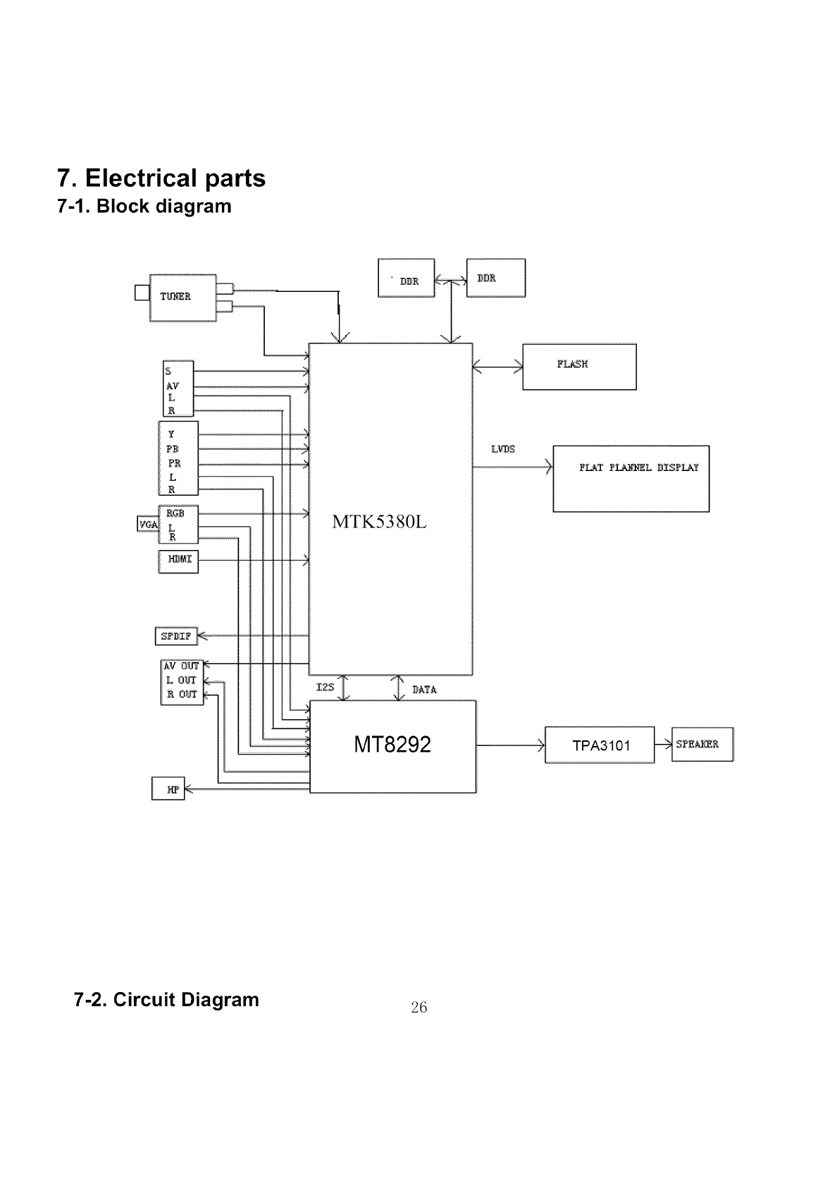
7. Electrical parts
7-1. Block diagram
T_E
:5
A¥
L
L
Y
PB
PE
L
R
m
m
m
MTK5380L
MT8292
DO_
L_S
YLAT T_L D_FLAY
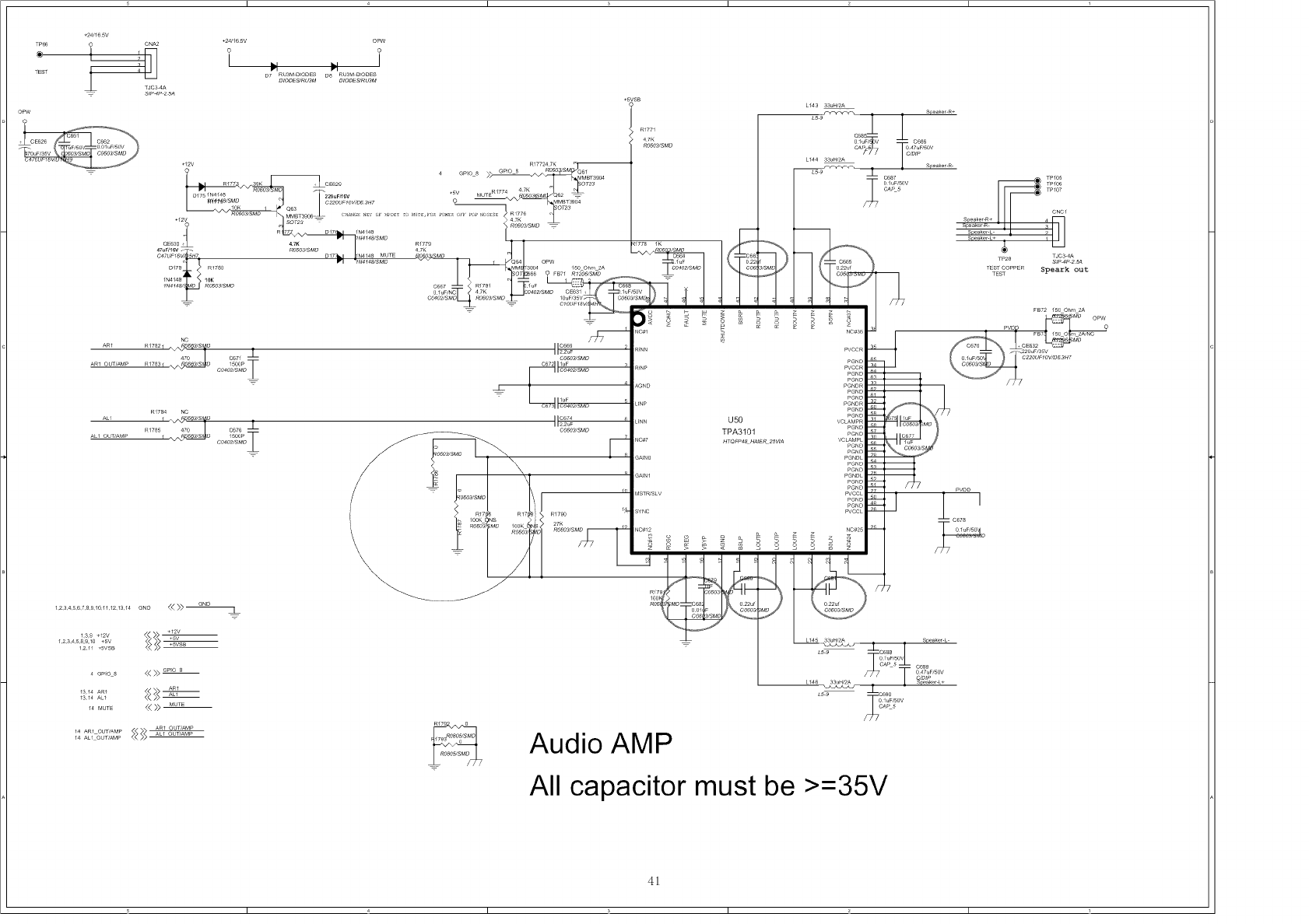
TPA3101
7-2. Circuit Diagram 26
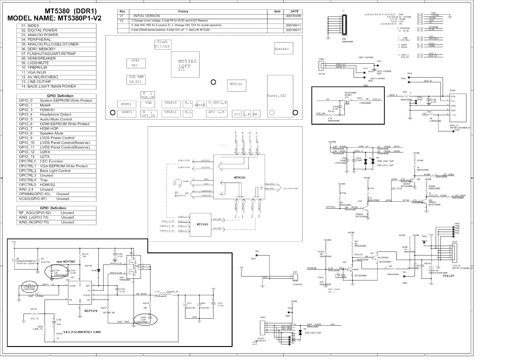
1 F 1 F
MT5380 (DDR1)
MODEL NAME: MT5380P1-V2
+/2V
o
leo
01. INDEX
02. DIGITAL POWER
03. ANALOG POWER
04. PERIPHERAL
05. ANALOG PLL/USB2.0/TUNER
06. DDR1 MEMORY
07. FLAS H/JTAG/UART/I R/TRAP
08. HDMt/SPEAKER
09. LVDS/MUTE
10. YPBPR/L/R
11. VGA IN/LR
12. AV IN/L/R/CVBSO
13. LINE OUT/HP
14. BACK LIGHT/MAIN POWER
GPIO Definition
System EEPROM Write Protect
GPiO1 Mute#
GPiO3 HDMt/Sl
9_!9:::::::4............................ ..................................................................................
P?!°::::::,5............................. ....................................................................
GPtO6 HDMt EEPROM Write Protect
GPiO7 HDMt HDP
GPiO8 Speaker Mute
GPIO 9 LVDS Power Control
..................................:::::::.......................................................................................................................................................................................................
...... !0:::::::! _ _/ PA_ e2 c e n t[o I(R e s e rv e ...................
GPiO11 LVDS Panel Control(Reserve)
GPtOoo12 U2RX
GPiO 13 U2TX
OPCTRL0 CEC Function
OPCTRL1 VGA EEPROM Write Protect
OPCTRL2 Back Light Control
OPCTRL3 Unused
OPCTRL4 Trap
OPCTRL5 HDMt/S2
AIN1,2,4 Unused
OPWM0(GPIO 40) Unused
VCXO(GPIO 67) Unused
GPIO Definition
RF AGC(GPiO 62) Unused
AIN3 L(GPIO 74) Unused
AIN3 R(GPIO 75) Unused
0.8 x (1+2.49KJ470) =5.04V
/K
Rev History Note DATE
V1 INITIAL VERSION 2007/04/09
V2 1 Change Vcore Voltage 2Add FB for DV33 and AV33 Reserve
3 Add R49, R50 for A version IC 4 Change C20, C21 for crystal capacitors 2007/06/11
5Add DRAM Serial resistors 6Add CEC uP 7 Add U16 MT8292 2007/06/11
HT5380
LQFP
u13
o
MT8292
T
TP6
TEST
CON2/NC
C701
01uF
Jl
EM_/HAJER
234567891011121314,15 GND
24,7,8,9,10,13 _SVSSB
2,/1,/5 _SVSB
S,9,/5 +/2V
234S891015 +SV
40PWRSB
I0 _R_N
40PCTRLS
4 ADEN1
4 ADEN2
+I2V
_ ADEN1
ADEN2
CNE2
D! .......
ADN2 KI
PH 3H
TEST
TEST
m
C74
DVOPW R_I_
R21_ luF
47K
RO603/SMD
_ aPo 3
4 GPO 3 _5D
TEST COPPER DVD 5V
TP23
_ TEST COPPER
__ DVD 5V ]
GP'O 3 v_ TP93 _ /
FB11
+12V
+3V3SB
....../ f.....4 d .........
co2_1 /_co29 J_ D_.b D3
loop /00pF ESD O4O2 10pF R1695
_ _ RO60S/SMD
R169 0 LED GRE#
...... +5Vc_Bt __R16 747K Q51 +5VSB RO603/SMD
R1698
_1707 L# _ ROGO3/SMD
1708 /a
OVOPW R16_ 0 LEDRED#
7k _O_03/SMD
O53 O_03/SMD LED#
Ok 2NS904
O_03/SMD SOT23/SMD
OPCTRL3 /0 _ 709
2NS_04 "
TP87
PSg
Pg0
+5VSB p_l
© +5VSB +5VSB +/2v
TP20
R0603/SMD R398/K t t 3U_TjC 3
NC NC_4 7K Q2
R060 _SMD 9
__CE6
Q27 1 F 7A
sD ;_ / 4_'_TP3 c 70UFI6V/D/0H9
_5VSB
TP"
CNEI TEST
_oo_o
, ESD 0402 /0pF
T 81
PH_5H
• A I B I c I D I E "
+5V
9
U1 AZ1117/adj
SOT223/SMD DV33 AV33
3 C_ L134
I,. 5 ouTI.... t __
NS/FB
A 1 1 1_,_o,o_o,1
yJ 110_°/o _CE71 _ CE1 / Os_3 ', I CB37
S 20uF/16v 100uF/16V --
1f__000_,_yO2200F10V_,000F10V,O_._oF _%.10F
_o__Z-__ r_,°_'s_==o_o_,s_o
U3
AP1513/SOP-8
+SV or _12v SOP8/SMD DV10
I i!,
R518 C301 O/P C302 R_
3K 0.1uF 1O0nF 1K t "
| | _ R0603/sMDTc0402/SMD;3 | C0402/ RC CB5 CE33 CE9 ", CB42
lOOoF,lOV --_--0.1oF> lOOK / _ >> _ Tco402,s_%_F'4_OoF,lOV,_ C470UF16V/DT_;0402/SMD
,O--OA .....
LOW ES
O_4
I 0.1uF
7
C0402/SMD 0.8 X(1+1_2K) = 1.2V
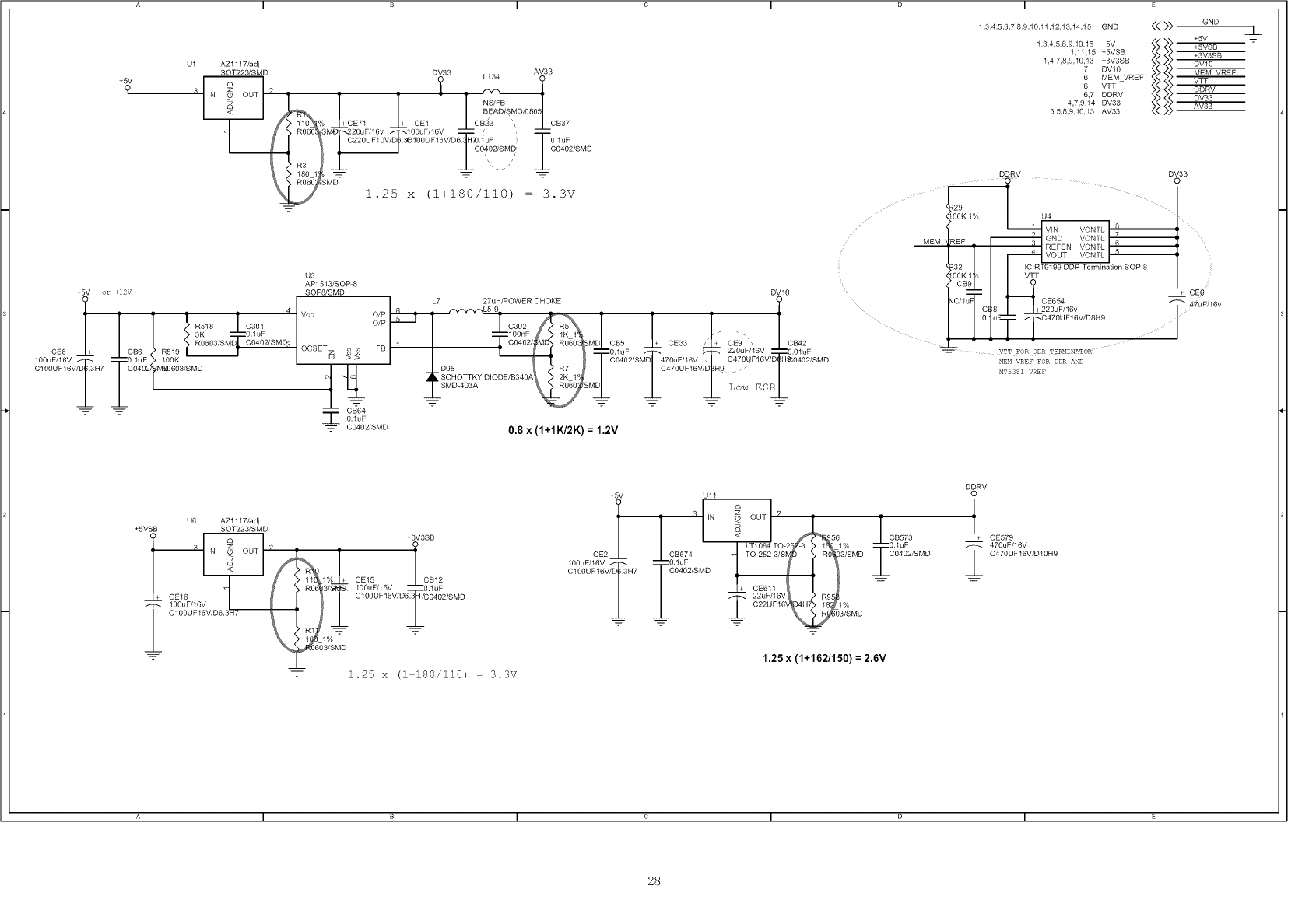
1,3,4,5,6,7,8,9,10,11,12,13.14.15 GND
1,3,4,5,8,9,10,15 +5V
1,11,15 +5VSB
1,4,7,8,9,10,13 +3V3SB
7 DVl 0
6 MEM VREF
6 VTT
6J DDRV
4_7_9_14 DV33
3,5,8,9,10,13 AV33
DDRV DV33
100K 1%
_R32 IC RT9199 DDR Termination SOP-8
100K 1 o VTT
C
CE6
/C/I_'F_ CE654
C _ 220uF/16v
VTT FOR DDR TBP_MINATOR
HEN VREF FOR DDR AND
MT5381 VREF
GND
+5V
+5VSB
+3V3SB
DV10
MEM VREF
VTT
DDRV
DV33
AV33
1
+5V Ull
o
U6 AZ1117/adj _ - 3 IN
+5VSB SOT223/SMD 9 +3V3SB i i
i !c1E_u!U/_ VV/D 6 C100UF16V/D6"3_ 7C0402/SMD _
= _o;:go =
1.25 x (1+180/110) =3.3V
DDRV
< I ¢561 _ CB573 CE579
q LT1_84 T/O_2 -3 ,03_;MD _;_0F/sMD 4C7407;F/_IVv/D10H9
1.25 x (1+162/150) = 2.6V
• A I B I c I D I E "
28
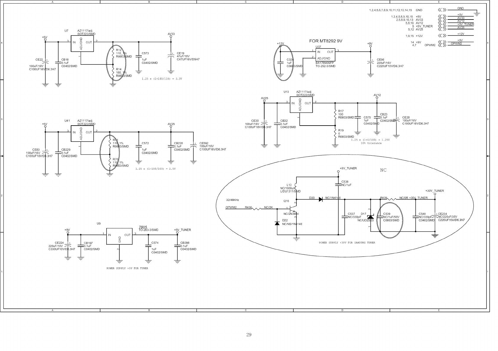
U7 AZ1117/adj
SOT223/SMD
+_v __
CE22 _ CB18
_ O.luF
100uF/16V 71CO4O2/SMD
C100UF16\ 'D6.3H
' Rt2
' 110
__,RO6O MD
' R14
, 180 Y_
MD
AV33
IC573 l_ CEt9
_ 7uF/16V
1pIF C47UF16V/D5H7
04O2/SMD
1.25 x {i_180/ii0) = 3.3v
+12V FOR MT8292 9V
3
+9V
i CE96
1,2,4,5,6,7,8,9,10,11,12,13,14,15 GND << >>
2,5,8,9,10,13 AV33
5,8,10 AV12
+5V TUNER
5,12 AV25
1,9,15+12v <<>>
14+9v _4,7 OPWM2
i 220uF/16V
C220UF10V/D6.3H7
GND J_
+5V _
AV33
AV12
+5V TUNER
AV25
+12V
+9V
OPWM2
U41 AZ1117/adj
+5V SOT223/SMD
,N_OUT_ A
1%
3/SMD
CE83
100uF/16V
C100UF16V/D }.3H7 CO4O2/SMD
t%
3/SMD
_-- _ 7
AV25
_ 100uF/16V
1.25 x {i_i00/i00) = 2.5V
U9
9v I I °033sMDrER
CE224 CBt97 C574 CB398
220uF/16Vy_ O.luF i TC _.luF
0330UF1OV H7 I;O4O2/SMD 1;Fo2/SMD O4O2/SMD
AV25
o
CE3O
100uF/16V f_
C100UF16V/DI.3H7
U10 AZ1117/adj
SOT223/SMD
: 3 IN _ OUT ?
CB32 t
Z0.1uF
CO4O2/SMD
AV12
! 1
RO603/SMD C575 O.luF CE28
o_L_F°_'t°°_°_'sl_°°°_Vv'__
R0603/SMD
1.25 x {l_O/1OO) =1.25V
10% tolerance
L3I
NC/1OOOu
L/DU1311 D
32/48KHz , Q16@41t NC/2N39 4
D22
NC/N 8
D20 ii.I NC/1N41,
P"I +5V_TUNERc538_ - NC °_c _,
_NC/1uF
+3OV _UNER
1 JR439,N/N./, NC/0R +30 TUNER
T tq ,ov)NC/33OpF..NC/22OuF/35V
N°'33%uo Too402,sM:,
•AI BI CI DI E"
29
DV33
R39
4.7K
RO693/SMD
OSDAO
OSDA0
OSCLO
OSDA1
OSCL1
OPWM0 1 q,q
OPWMI 2o4
OPWM2 ?0,_
VCXO 148
OXTALO 14,5
OXTALI 146
AVCC SRV 14q
AVDD33 XTAL 147
ADIN4 154
ADIN2 @
ADIN1 1,51
PWRDET 1,50
AVDD33 REG 88
C XREG 07
ORESET# 71
OPWRSB 7 _
DV33
U13B
m06 OSDA0
207 OSCL0 GPIO 0
0,3 OSDA1 GPIO 1
0_ OSCL1 GPIO 3
OPWM0 GPIO 4
OPWM1 GPIO 5
OPWM2 GPIO 6
VCXO GPIO 7
XTALO GPIO 8
XTALI GPIO 9
AVDD33 SRV GPIO 79
AVDD33 XTAL GPIO 11
GPIO 12
ADIN4 GPIO 13
ADIN3
ADIN2
ADIN1 OPCTRL9
ADIN0 OPCTRL1
OPCTRL2
AVDD33 REG OPCTRL3
C XREG OPCTRL4
ORESET OPCTRL5
OPWRSB
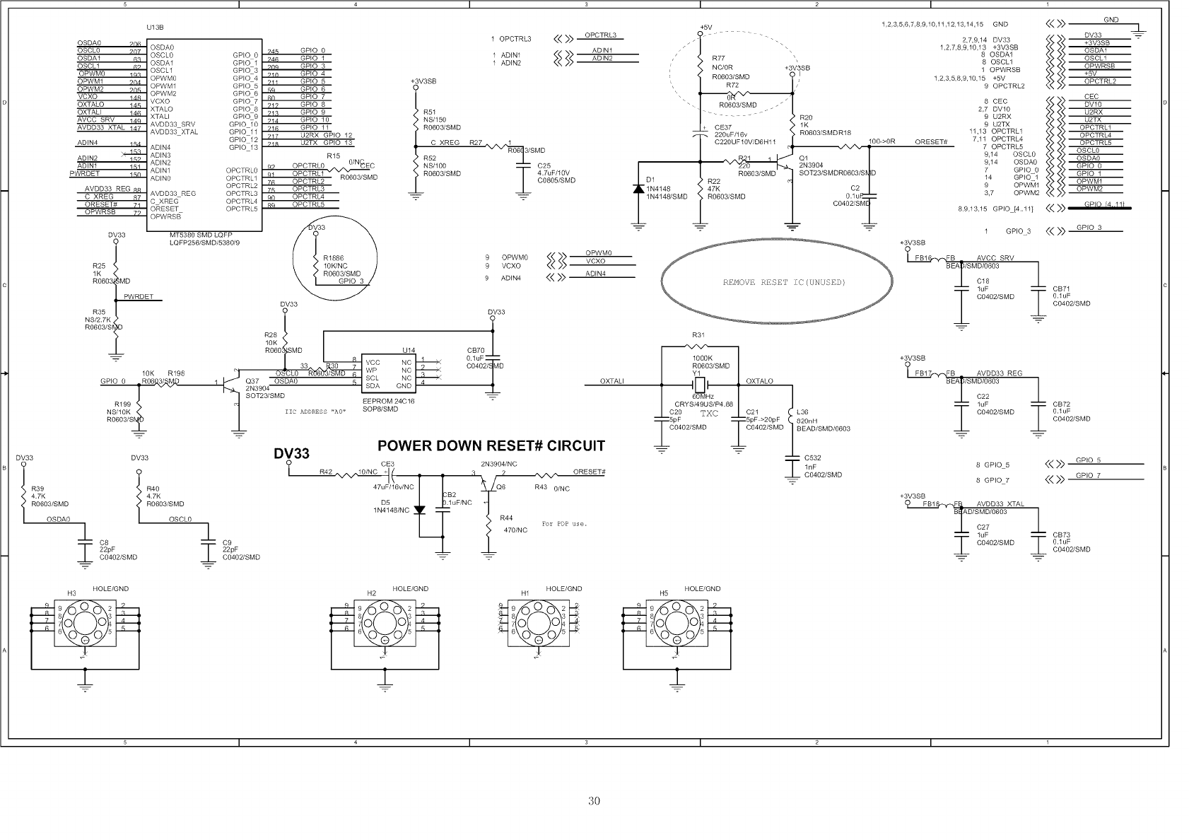
MT5380 SMD LQFP
LQFP256/SMD/5389/9
R25
1K
R060 ." MD
PWRDET
24,5 GPIO 0
246 GPIO 1
?0q GPIO 3
710 GPIO 4
?11 GPIO 5
,_q GPIO 6
60 GPIO 7
212 GPIO 8
21,3 GPIO 9
_14 GPIO 10
?16 GPIO 11
717 U2RX GPIO 12
_10 U2TX GPIO 13
R15
9? OPCTRLO 0/N_Ec
91 OPCTRL1 R0603/SMD
76 OPCTRL2
75 OPCTRL3
90 OPCTRL4
0q OPCTRL5
DV33
+3V3SB
10PCTRL3
1 AD)N1
1 ADIN2
R51
NS/150
R0603/SMD
C XRE..___.GR27 v,N/,,__/SM D
R52
NS/1OO C25
RO603/SMD I 4.7uF/1OV
C0805/SMD
(( _> OPCTRL3
ADIN2
_ OPWM0
9 OPWM0 VCXO
9 VCXO
9 ADIN4 << >> ADIN4
NS/2.7K,
R0603/S_
'>R28
10K
R060 MD U14 CBT0
----_-- 0.1uF
- 33 30 !, CO4O2_IM_D
1OK R198 _ O O
GPIO 0 .RO6_3/_M_.___, ---_ Q37 OSDA0 ,51_ ,J,,',_I 4 -
2N3904
SOT23/SMD/ /
S_[_ 1 _EPROM 24018
Ns/R_99 zzc ADDRgSS "A0" SOP8/SMD
R0603/
/C8
I22pF
C04O2/SMD
HOLE/GND
H3
)
+5V
/
_ R77
NC/0R +3V3SB
RO603/SMD
_, R72
RO603/SMD . i _ _
.... R20
CE37 1K 9 U2TX
RO693/SMDR18 11_13 OPCTRL1
C229UF19WDSH11 _ 190->9R ORESET# 7,11 ©PCTRL4
c70PCTRL5
1 Q1 9,14 OSCL0
2N3904 9,14 OSDAO
R22 RO693/SMD SOT23/SMDRO693/S D ^7 GP)OOD1 14 GP)O 1
OPWM1
1N4t48 47K __,7
1N4148/SMD RO6O 0.1u OPWM2
L....... 1 CO4O2/S_ 8,9,13,15 GP'O [4..11]
1,2,3,5,6,7,8,9,10,11,12,13,14,15 GND <_( _ GND
2,7,9,14 DV33 +3V3SB
1,2,7,8,9,10,13 +3V3SB OSDA1
80SDA1
80SCL1 OSCL1
1 OPWRSB OPWRSB
+5V
1,2,3,5,8,9,10,15 +5V OPCTRL2
90PCTRL2
CEC
8 CEC DVlO
2,7 DVl0 U2RX
9 U2RX U2TX
OPCTRL1
OPCTRL4
OPCTRL5
OSCLO
OSDA0
GP(O 0
GP(O 1
OPWMI
OPWM2
<<>> GPIO F4 1tl
H
FB_I FB mAVCC SRV
1uF CB71
1
OXTALI
DV33
R31
FB_17 FB mAVDD33 REG
BEA /SMD/9693OXTALO
t C22
luF CB72
C21 L36 I CO4O2/SMD I o.IUF
5pF->2OpF 820nil CO4O2/SMD
ICO4O2/SMD ICO4O2/SMD f EAD/SMD/O6O3 _
C532
I nF 8 GP)O 5 <_4__>_ GP)O 5
C9492/SMD GP)O 7
8 GP)O 7 _<_ _
R40
4.7K
R0693/SMD
OSCLO 1C9
I22pF
C04O2/SMD
POWER DOWN RESET# CIRCUIT
DV33
CE3 2N3904/NC
47uF/16v/NCI_,_ 2 06 R43 0/NC
D5 IuF/NC
1N4148/NC
R44 For PDP use.
HOLE/GND
H2
J
+3V3SB
F?.___.._._F_ AVDD33 XTAL
IuF CB73
Z CO4O2/SMD I o.IUFCO4O2/SMD
HOLE/GND
H1
)
HOLE/GND
H5
)
i i i
• _ I 4 I 3 I 2 I _ "
30
] F ] F
UI3D
AVDD12 ADCPLL /f! _
USB DM _ USB VRT AVDD12 PLL USB VR
tiff USB DM AVDD12 TVDPLL /fi 7 T@ 603/SMD
AVDDI2HDM_PLL _55 AVDD12 PLL
AVDD33 USB _6 USB DP AVDD12 PLL NS/_OOpF
AVDD12 USB 67 AVD533 USB AVD512 APLL /_3
6 q AVDD12 USB AVDD12 STSPLL /_1 AVDD12 PLL C0402/
TP0 AVDD12 DMPLL _5_ AVDD12 PLL
AVDD12_TDPLL /5_ AVDD12 PLL
MT5380SMDLQFP
LQFP256/SMD/5380/9
AV33
_ AV25
FB A DD33 USB AV12 FB34 FB
_ "m _ ............ .......... _ _ _ _ l
B_D/ _y_ A_D[ B_D/ MD/0805 A DD25 SADC
BEAD/ MD/0603
47UF/10_ CB87 C54
/C0805/SvluI F ....
.............T .T Tc'.T' .....
J_ J_ 0 luF C0402/SMD C0805/SMD 0 01uF 0 luF
T _ C0402/SMD AVSS25 SA C0402/S C0402/SMD
UI3H
/_ 5 AVDD25 SADC
AVDD25 SADC /_ AVSS25 SADC
.............
AF
TUNER DATA In7 RF AGC RI 9" 10K F AGC
TUNER CLK TUNER DATA F AGC MD
/nil TUNER-CLK C568
MT5380 SMD LQFP 0402/SMD
LQFP256/SMD/5380/9 _C0 +5V
AV12
FB19 FB AVDD12 PLL
_Y_ BEAmtC41 C31...... 1 1
i c0402/SUD C0805/SMD 001_F 01_F
C0402/S C0402/SMD
AV12
l USB_5V
i /0ouF/16v
C/OOUFI6V/D5 3H7 USB ON
USB DP
CE228
220uF/16V
i C470U FI 6V/D8H9 D37 D36
ES_0402 0 15pF ESD O4O2 015pF
C0402/SMD C0402/SMD
F_
+SVTUNER
_T_ C T 5V • .SVF
CB1004 E31 NC
_470uF//6v >220u_ SOL
SDA
NC NC
AS F
FAGC
DF
NC D_F
/_ GND
GND
GND
GND
rl
DTV 8ADC/GW41F2
DVT-SADC/GW4 / F2
±
TP/2 _ USBOPWRERR
SOT2S/SMD _'os¸' P_JS_¸
F;, "AO3401
+5V Q75
R2154 nanoSMDC/50F
20K RI206/SMD
R2155
USBOPWREN Q76
2N3904
USB+5V U_B+5V
R2028
4 i# _,v_ 560R TUNER SCL
5 _ _" .... Li _-- ........
.... '£o°?
T AGC 68K C696 C692
q Q/ _F A_C 33pF 33pF
/q DFAT _ TC0 02 _C0 02 SI '
...... _+ _ .... _ _
°,V4....
.... ....>./
+5V TUNER
TUNER
.....................
b_@ R168
4 7uF/10V/ NC//0K
C/08
R173
/NC//0K
_5V F
RF AGO 3 /
T SCL
T SDA
_/ T AGC
DFATN+
+5V TUNER
R1624
TUNER DATA
TUNER CLK
T 5V
AS
SCL
ANT POWER SDA
÷5V TUNER AS F
1_ FB48 F AGC
DIF
+30V TUNER FB/NC _ VT D_F
D GND
C/FB GND
GND
TDI636EF MK2
IF USE T1 (DTV 8ADC/GW4ZF2) , TD/636FV
FB48 SHOULD B_ N/C.
SIF LEVEL SHIFTER
Near Tuner Near MT538X
C43 C/47 27 F
DFAT N+ A _ _Y_ .
" _ II L14 dUOnH l_ IL2123L23 220nH
C142 L21
1_012 i 33pF _dUOnH
oR , i_
DFAT_N _
i 33pF
L24 C208
4 7pF
NC _ TC0402iSMD
Use muRata Inductor and TDK Capacitor
GND dividing
FB22 NSIFB FB58 FB/NC FB39 FB/NC F_I NSIFB
B B B
SIF LEVEL SHIFTER
12346789101112 13 I4 15 GND << _
3,8,10AV12 T
I¸2¸3¸4¸8,910,15*SV
247 _14 DV3S
312 AV2S
3 +SV TUNER AV33
23¸8¸9¸I013AV33
14 DVDD _ )) DVDD
MOP_O4 8292 MOP_O4 USBOPWREN
_4s:9=M_p:o4 <4>? ._P:os s_g_._P:os USBOPWRERR
I4 8292 MGPO3 %, 22 .....
12 VP ATV V_V
12 VN ATV
31
RDQS0 11
RDQM0 13
RDQ0 9
RDQ1 6
RDQ2 7
RDQ3 6
RDQ4 ,5
RDQ5 4
RDQ6 3
RDQ7 ?
RDQSI 17
RDQMI 15
RDQ8 19
RDQ9 _0
RDQ10 71
RDQ11 ?p
RDQ12 _3
RDQ13 _4
RDQ14 ?,5
RDQ15 _6
MEM VREF 53
RCS# 46
U13A
RDQS0 RA0
RDQM0 RA7
RDQ0 RWE
RDQ1 RBA0
RDQ2 RA6
RDQ3 RBA1
RDQ4 RA5
RDQ5 RP_S
RDQ6 RA8
RDQ7 RA10
RDQS1 RA4
RDQM1 RCAS
RDQ8 RA12
RDQ9 RCKE
RDQ1O RA11
RDQ11 RA9
RDQ12 RA3
RDQ13 RA1
RDQ14 RA2
RDQ15
RCLK0
RVREF0 RCLK0
RCS
MT5380 SMD LQFP
LQFP256/SMD/5380/9
47 RA0
36 RA7
4Q RWE#
43 RBA0
37 RA6
44 RBA1
36 RA5
4? RRAS#
35 RA8
45 RA10
39 RA4
41 RCAS#
3? RA12
31 RCKE
33 RA11
34 RA9
51 RA3
4q RA1
_Q RA2
_6 RCLK0#
?9 RCLK0
MEM ADDR12 6 _ 7 RA12
MEM ADDR11 6 _/NiN. 5 RA11
MEM ADDR9 4 _AA 3 RA9
MEM ADDR8 47x4 RN04.0"2^v^ v 1 RA8
RN0402/SMD
MEM ADDR7 47x4 R_0_(_2/_KJ_2 7 RAT
MEM ADDR6 RN040_/S D_._A _ ,5 RA6
MEM ADDR5 4 'N/N/N. '3 RA5
MEM ADDR4 _ _N/N/X, 1 RA4
MEM WE# 47x4 R_0_2_N_3 7 RWE#
MEM CAS# RN040_/S DM_,_ ,5 RCAS#
MEM RAS# 4 .V_ ;;_ RRAS#
MEM Ros MEM BA0 5 RBA0
MEM BA1 4 "v'N/N. 3 RBA1
MEM ADDR10 47x4 _ _ 1 RA10
RN0402/SMD
MEM ADDRO 47x4 6 _/I_N_5 7 RA0
MEM ADDR1 RN040R/S 4DM_ 5 RA1
MEM ADDR2 4 .'-.,/,.,,% 3 RA2
MEM ADDR3 ?_ 1 RA3
DDRV ]
I I_.fll iA3 tA4 tA8 _8 $____4.TuF/10V I
CEA1 CA7 A43 CA35 I
o Ly88.3v7_ oFTloF-- oF-- oFTloF o.1oF O0 0 ,SMO'
i-C0402/S_D -C0402/SMD _C0402/SMD I
[ C0402/SMD C0402/SMD C0402/SMD C0402/SMD
VTT
iCA17 ICA19 ICA20 ICA21 ICA22 ICA28 ICA23
TS F2,s DT°. oF,S T°. oF/SMDT oF,SoT oF,SoT oF,So o ;o I°vD
DDRV DDRV
MEM DQ0
MEM DO1
MEM DO2
MEM DO3
MEM DO4
MEM DO5
MEM DQ6
MEM DO7
MEM DOS0
MEM ADDR13
MEM DQM0
MEM WE#
MEM CAS#
MEM RAS#
MEM CS#
MEM BA0
MEM BA1
MEM ADDR1O
MEM ADDR0
MEM ADDR1
MEM ADDR2
MEM ADDR3
?
4
5
7
6
1Q
11
13
16
17
?1
?4
77
?6
?9
36
3t
3?
qq
RCKE
UA1
VDD VSS
DQ0 DQ15
VDDQ VSSQ
DQ1 DQ14
DQ2 DQ13
VSSQ VDDQ
DQ3 DQ12
DQ4 DQ11
VDDQ VSSQ
DQ5 DQ10
DQ6 DQ9
VSSQ VDDQ
DQ7 DQ8
NC NC
VDDQ VSSQ
LDQS UDQS
NC NC
VDD VREF
NC VSS
LDM UDM
WE CLK
CAS CLK
RAS CKE
CS NC
NC A12
BSO All
BS1 A9
A10/AP A8
A0
A1
VDD VSS
16M x 16 DDR TSOP-66
DDR#1
TSOP66/SMD
65
63
62
6O
59
57
56
54
51
4':)
47
46
45
44
41
46
39
,36
37
36
35
.ad--,
RAI_A 22 MEM CLKEN
R0603/SMD
MEM _Q14 _wap for layout
MEM
MEM DQ13
MEM DQ12
MEM DQ11
MEM DQ10
MEM DQ9
MEM DQ8
MEM DOS1
MEM VREF
MEM DQMI
MEM CLK0#
MEM CLK0
MEM CLKEN
MEM ADDR12
MEM ADDR11
MEM ADDR9
MEM ADDR8
MEM ADDR7
MEM ADDR6
MEM ADDR5
MEM ADDR4
RCLK0 RA12 _/N/N22 MEM CLK0
R0603/SMD / RA14100
RCLK0# RA13 _/N/N22 MEM CLK0# R0603/SMD
"R0603/SMD
C0402/SMD ! iC0402/SMDI c0805/SMD
1,2,3,4,5,7,8,9,10,11,12,13,14,15 GND ((_ GND J_
2 MEM VREF <<>> MEM VREF
- DDRV
2,7 DDRV _ VTT
2 VTT
VTT
O
RDQ047x4 6 _ 7 RN0402/SMD MEM DQ0 7 _ 678x4
RDQ1 6 _ MEM DO1 _ 6 RN0603/S
ROQ3 ?6AA 1 MEM DQ3 1 AA} ?
RDQ4 6 _ 747x4 MEM DQ4 7 _ 675x4
RDQ5 6 _ ,5 RN0402/SMD MEM DQ5 ,5 ./N/N/_ 6 RN0603/SM_
RDQ6 4 _ MEM DQ6 _ AA_ 4
RDO7 ?_ i MEM DO7 i _ _ _ ?
RDQS0 RA1 "N/N/N. 47 R0603/SMD MEM DQS0 _75 R0603/SMD].
_*_ _Ji "/N/N_47 R0603/SMD MEMDQM0 _RA_*'_V_*75 R0603/SMD_
RDQMI RA3 47 R0603/SMD MEM DQMI _/XN'* 75 R0603/SMD_
_47 R0603/SMD MEM DQSI _RA'_"_v'_.75 R0603/SMD].
RDO8 "_ ,.."N/N/" 1 MEM DOS 7 _R_ 675x4
RD°9 RNA84 _ 347x4 MEM D°9 5 ./N/N._ 6 RN0603/S M#
RDQ10 6 _ ,5 RN0402/SMD MEM DQ10 ,3 _ 4
RDQ11 6 jNix/_ 7 MEM DQ11 1 ?
RDQ12 7 _ 6 MEM DO12 7 _ 6 75x4
RDQ13 ,5 6 MEM DO13 ,5 6 RN0603 SM_
RD 14 ' _ MEM D 14 ' _ --
O _ _ 4 O _AA_ 4
RDQ15 1 _ ?MEN DQ15 I I1 _A_A_ ?
RNA10 47x4 I I v _
RN0402/SMD
VTT
MEM WE#
MEM CAS# 7 _ _ 7R5NX_603/SMD
MEM CS#
MEM BA0 7 75x4
MEM BA1 ,5 jNiN/_ RN0603/SMD
MEM ADDR10 3 _ 4
MEMADDR4 _ _ 75x4
MEM ADDR5 , 6 RN0603/SMD
MEMADDR6 _ _
MEM ADDR7 _N/N/"
MEM CLKEN RA_/_. NC/75
R0603/SMD
MEMMEMADDR11ADDR1231 _ 4?7R5NXc4603/SMD
MEM ADDR9
MEM ADDR8 _
MEM ADDR0
MEM ADDR1 7
MEM ADDR2 ,3 _ 4
MEM ADDR3 1
MEM ADDR13 _ /bx4
NC/'/'/'/'/'/'/'/'/'_RA 10 Hl_uuua/_wu
R0603/SMD
VTT
?
ICA24 ICA25 ICA26 ICA27 ICA30 1 CEA4
0.1uF 0.1uF 0.1uF 0.1uF M_.7uF/1OV T 100uF/16V
ToH402,sMTo0402,s_To0402,s_To0402,s_080_,s_oO100UF16V/D6.3H7
J_
• _ I 4 I _ I 2 I _ "
32
TTTT
POCEO#
POOE#
PDDO
PDD1
?,5P
?,51
?50
749
DVI 0
U13J
POCE0 UORX
POOE UOTX
PDD0
PDD1 OIRI
JTMS
JTRST
JTCK
JTDO
JTDI
MT5380 SMD LQFP
LQFP256/SMD/5388/9
JTDO R56
9_ UORX
94 UOTX
93 OIRI
7,53 JTMS
JTRST#
?56 JTCK
?,5,5 JTDO
?_4 JTDI
JTRST#
JTDI
DV33
tII
R0603/SMD
U17
POCEO# 1
PDDoR120 o _ot_
FRESE__s_VP
M25P32
CASON8/SMD
DUAL LAYOUT
DUAL LAYOUT
RN5
18K
RNO683/SMD
1
R54
18K
RO683/SMD
7
6
,5
U18
DV33 HOLD#
POOE# S VCC
PDD1 NC
PO2
PO1
POCEO# PO0
PDDO R12 CS#
_O/PO7
2MB MX25L t605/S25FL016A/NS
SO16W/SMD/MX25L6405
DV33
UORX
R45
4.7K UOTX
RO683/SMD
FRESET#
GPIO 0 R197 NC/ K Q43
NS/2N3904
SOT23/SMD
R200
NC/10K
POOE#
sc_KI_ _oD1
Sl
PO6
PO5
po4
PO3 GND
GND FRESET#
WP#/ACC
1,2,3,4,5,6,8,9,10,11,12,13,14,15 GND
1_2,11,15 +5VSB
1,2,4,8,9,10,13 +3V3SB
DV33 4,9 U2RX
4,9 U2TX
4,8 OSDA1
4,8 OSCL1
CB452 2,4,9,14 DV33
0 luF 2 DVl0
DCO482/SMD 2,6 DDRV
<<>> GND
+5VSB
+3V3SB
U2RX
U2TX
OSDA1
OSCL1
DV33
DV1O
DDRV
Rl_//%% URX
R0603/SMD \\//
Rl_// NN UTX
RO683/SMD \\ //
1
JTMS
JTCK
_x_ 33
RO603/SMD
R53
10K
R0603/S_
1
3
,5
Iw/IJTAG DBGRQ 7
JTAG DBGACK 9
R58 _ST_ R59
O10K { 10K
RO683/SM_ RO683/SMD
A
In
DIP5X2/2.0MM/NC
DIP5X2/P2.8
OIRI <<>> OIRI TT_ °
C0402/SMD
4 GP_oo <<>> GPIO0
11 +3V3SB TP102
DI _ TP183
11 R60 R61 TP104
CNB2R62 R0603/SM
UOTX _100
* 2_
FOR CODE DOWNLOADAND DEBUGGING PH3-4A
-- SIP-4P_2.OA
U131
VCCK VCC210
VCCK VCC210
VCCK VCC210
VCCK VCC210
VCCK VCC210
DVDD10 VCC210
DVDD10 VCC210
VCCK VCC210
VCCK VCC210
VCCK VCC210
E_PAD
E_PAD VCC310 3
E-PAD VCC310 3
E-PAD VCC310 3
E-PAD
E-PAD E-PAD
E PAD E-PAD
MT5380 SMD LQFP
LQFP256/SMD/5388/9
DDRV
U
DV33
DV33
R1 5 NC/4.TK OPWM2 4.7K 1 86
RO683/SMD R868_
R1 2 NC/4.TK AOBCK 4.7K 1 55
R0683/SMD R8683
4.7K->47K AOLRCK NC/4.7 1 57
RO683/SMD R8683/
+3V3SB
R1 2 "-4.7K OPCTRL4 NC/4.7 226
RO603/SMD RO6O3/S
R1 2 4.7K OPCTRL5 NC/4.7 1 27
RO683/SMD R8603/
Trap Mode OPWM2 AOBCK AOLRC K
Normal mode 0 0 0
ICE mode O O i
Core Reset 1 us 1 1
DV33
iB34 IB35 IB36 L.76uF/1OV ____IC4F5
CO4_S0_;F CO$S0_;F COTS0_;F j OO8O_,SMD|OO402,SMD
i/o BYPASS
40PCTRL5 OPCTRL5
3,4 OPWM2 OPWM2
13 AOLRCK AOLRCK
13 AOBCK AOBCK
DV1O
t
10_4 iD4_It_81 t_82 t_83 t_84 t_88 1_8_ t_80 t_88 1_8_
_[_o_il_&%%2,_mO.loFTO.loF To.loF TO.loF TO.loF TO.loFTO.loF To._oFTo.loF
t _ Cq402/}MD CO4O2/}MD CO4O2/S_D CO4O2/S_D CO4O2/S_D CO4O2/S_D CO4O2/S_D CO4O2/S_D CO4O2/S_D
LCORE BYPASS Near IC
]
tA37 tA38 tA39 tA4O tA41 tA42 tA4_
To.luF To.luF To.luF To.luF To.luF To.luF To._uF
D_CO4O2/SMD _CO4O2/SMD _O4O2/SMD _CO4O2/SMDA_402/SMD[ nn,_n?lSMgt
- - - DDR BY-?ASS Near IC_ -
DDRV
oo8o ,sT oo4o2,S%o4o2,s,
± -
• _ I 4 I 3 I 2 I _ "
33
RX0CB N
RX0C N
RX00B N
RX00 N
RX0 IB N
RX0 I N
RX02B N
RX02 N
UI3K
i
7R RX0CB EXT REsLZZ_<
nq RX0C OPW_ SV 7_
nl RX00B
n? RX00
n_ RX0 18
n_ RX012
n4 RX0 I AVDD33HDM_
n_ RX028 AVDD12CVCC
Ur53S0SMOLQFP
LOFP256/SMD/5380/9
OPWR0 SV
AVDD33 H
AV33HDM_
RO402/SMD T
RX0 CB _NR2 ./_ 5O RX0 CB
R0402/SMD
RX0 C _N R4 _/_ 5O RX0 C
R0402/SMD
_ R0402/sMDRX0 0B _ C710
RX0 0 _N _V._50 RX0 0 _uF//SV
R0402/SMD l
RX0 IB _NR3S _ 5O RX0 IB
R0402/SMD
RX0 I _N _50 RX0 I
R0402/SMD _
RX0 2B _NRS7 _/_ 5O RX0 2B
R0402/SMD
RX0 2 _N _v_,50 RX0 2
+3i3SB
FBBEAD/SMD/0603 AVe3
BEAD/SMD/0603
C711
OuF//6V
+3V3SBQ D153 R1605
J/._I ....
RB520S 30/NC 27K
__ 11_K HDM{3 HPD
_ HOM_35V_N
HOM_3OOC SOA 8 _
m ONe3OOC SCL
_? HOM_3R×_
_'1 HOM_3R×C+ _
HOM_3R×0
a__
• HOM_3R×0+
__ HOM_3R×_
4 HOM_ _×_÷
AV33HDM_ _ _
R212G _ _ __ _
AV33_OM_ _
H
HDM2 RXC
HDM2 RXC+
HDM2 RX0
HDM2 RX0+
i_ _ 13_'/N/ 1_40M4 HPD HDM2 RXI.
HDM2 RX/+
HDM4 DDC SDA HDM2 RX2
HDM4 DDC SCL HDM2 RX2+
R2139 0 CEC HDMI RXC
/9 _ HDM4 RXC HDMI RXC+
/q HDM4 RXC+ _ _ HDMI RX0
HDM4 RX0 HDMI RX0+
a__
7 HDM4 RX0+ HDMI RXI-
L HDM4 RXI- HDMI RX/+
4 HDM4 RX/+ HDMI R_
3 HDM4 RX2 HDMI RX2+
2-- HOM4 RX2+
VERTICAL MOUNT
023_ _IIS_ /
, 024_ _ /
, D24_ _IIS_ /
ESD0402 015pF
, D24_ _ /
, D24@ _ /
, D23@ _IIS_ /
ESD O4O2 015pF
HDM4 RXC
HDM4 RXC+
HDM4 RX0
HDM4 RX0+
HDM4 RXI-
HDM4 RX/+
HDM4 RX2
HDM4 RX2+
, D22_ _ /
ESD0402 015pF
, D22_ _11_ /
, D23@ _11_ /
, D23_ _IIS_ /
ESD0402 015pF
HDM2 RXC
HDM2 RXC+
HDM2 RX0
HDM2 RX0+
HDM2 RXI-
HDM2 RX/+
HOM2 RX2
HOM2 RX2+
021@ _11_1_ / HDMI3 RXC
021_ _11_ / HDMI3 RXC+
021_ _IIS_ / HDMI3 RX0
D21_ _ / HDMI3 RX0_
ESD 0402 015pF
D23_ _1_ / HDMI3 RXI-
D23_ _11_ / HDMI3 RX/+
D23_ _11_ / HDMI3 RX2
D23_ _S_ / HDMI3 RX2+
ESD O4O2 015pF
D20_ _11_ / HDMII RXC
D21_ _11_ / HDMII RXC+
[}21% _11_ / HDMII RX0
D21_ _ / HDMII RX0_
ESD 0402 015pF
D21_ _11_ / HDMII RX/+
D21_ _11_ / HDMII RX2
D22_ _ / HDMII RX2+
ESD O4O2 015pF
?
n
q
N
m
¢:----%
/n
74
,_1_-_-
vcc
BRXCM
BRXCP
vss
BRXOM
BRXOP
vcc
BRXIM
BRXIP
vss
BRX2M
BRX2P
vcc
ARXCM
ARXOP
vss
ARXOM
ARXOP
vcc
+sv
R2079 _ R2080
47K 47K
R2081 100 GPO 7
1oo OPWR0 5V
o OSDA1
0 OSCLI
, Do
AW3 HDMI
/OK/NC
AV33 HDM_
U8 •
ATb354
3FPIO0
CRX2M
vss _}1
ORXIP
CRmM
VCC --
ORXOP
CRX0M
VSS _
OR×OP
CRXCM
VCC --
DRX2P
DRX,2M
vss _
DRXIP
DRXIM
vcc --
ARXIM DRXOP
ARXI P DRXOM
vcc vcc --
ARX2M DRXCP
ARX2P _ DRXOM _ I
vss o _ _ _ vss _ _,
R2148 _
HDM3 R_+
HDM3 R_
HDM3 RX/+
HDM3 RXt.
HDM3 RX0+
HDM3 RX0
HDM3 RXC+
HDM3 RXC
' HDM4 RX2
HDM4 RX2.
HDM4 RXI+
HDM4 RX/
HDM4 RX0_
HDM4 RX0
HDM4 RXC
HDM4 RXC
AV33 HDM_
=/0PF >/SPF
AV33
FB35 FB AVDD33 H
CB145
01_F
C040SSMD
A_
FB20 FB AVDD12 CVCC
C/7 CBI4S
l ......... I ........ I ....
C0805/SMD C0402/SMD
CON44
SHELL2
SHELL4 HPDET n
_SV
GND
DDCDATA m
DDCCLKNc_m
CEC /?
CK
CKShed
CK_ /'1
D0 q
DOShield
D0_ •
DI _
Ul Shield 4
Dl _
D2 _
D2Shield /
_2-- SHELL3 D2*
HDM_con
12345679101112 13 1415 GND
123,4,S,_JOlS +SV
2 3 S9 10,13 AV33 AV12
35¸I0 AV12 OSOA1
4 OSOAI OSCLI
4 OSCLI CEC
4 CEC +3V3SB
+12V
MUT_I
AR1
49131S GP_O [411] _
HDM DDCSCL 0 OSCLI
HDM DDCSDA 0 OSDA1
<<>> _No
//lf......
_7
4 9/4 OSCL0 OSDA0
4914 OSDA0
__ 12_'/N/'IK HDMII HPD
_ HOM_I5V_N
HOM_IOOCSOA 8
ONe100C SCL
_V,,0 CEC
HDM_IRXC
HOM_IRXC+
HOM_IRX0
HOM_IRX0+
HOM_IRXl-
HOM_IRX/÷
HOM_IRX2
HOM_IRX2+
CON45 _H
SHELL2 _214_,/,_ 1 K HDM2 HPD
SHELL4 HPOET_5v _ _ _ HDM2 5VN
GND HDM2 DDC SDA
DDC DATA DM2 DDO SOL
DDC CLKNc_/_
CEC / _V_2 CECHDM2 _C
CK
CK Shield HDM2 RXC+
OK q_ HDM2 RX0
DO
D0 Shield HDM2 RX0+
DO • HDM2 RXI-
D1
O1 Shield HDM2 RX/+
D1_ 4 HDM2 RX2
D2 3
D2 Shield / HDM2 RX2+
SHELL3 D2+
HDM Don
HORIZONTAL MOUNT
HDMI RST R215_V_47K
TTTTTTTTTT°IT°IT°IT°'T°IT.....
J- 34
AVS38DM_ CHANGE GPiO 6 TO RESET HDHI SWITCH
GPIO 6-1 RESET
GPiO--6-O NORMAL
Rese_ time Pis. ref IC'S SPEC.
A0N _44
A0P 943
AlP _ 1
A2N _a
A2P ;_CKIN
A3N
A5N _ q
ASP _a
ASN _
A6P _7
CK2N _
A7N ??
A7P ??3
A0N AVDD33LVDSA
A0P AVDD33LVDSB
AIN AVDD33LVDSC
A2P
CKIN
CKIP TP2
A3N TN2
A_P
CK2N
CK2P
AFN
ATP
MT5380 SMD [QFP
LQFP256/SMD/5380/9
] F ] F
131415 GNO (<>>
/315 _12V +SV
1234581O15 +W
23581O13 AV33
124781O13 *3V3SB
481315 OPO [4 11]
AV33
4 OPWMI _ _ OPWMI
CE580
??? AVOO33 LVOS
AVDD33 LVDS
9_q AVDD33 VPLL
AV33
FB37 FB AVDD33 LVDS
CSS CSS
7UF/10V CB155
2......... Tc ........ Z ....C0402/SMD
/NT]_
4 ADN4 << >> ADN4
OPWM0
4 VCXO +_3SS
............. ll
4,i4 _S_A0 _ O_A0
4 U2TX
I OV_ 5V _ )) 0V0 5__
U2RX R210_. /00
AOSDATA0
_46 47K PE_
_0_03/SMD CNE4
MS0 PREST ADIN4 R2105 /00 / U
MS0 CLK VCXO U
AOMCLK _1U1
MS0 PWN "_
M80_NTO OPWMON21US_
PH_6_NC
S_P_P 2 0A
+5V
0
I
I
A7P A7N
A6P A6N
TP65 ASP
CNE3 _ A4p
LVDS OUT QF3
FB12 ¢_¢'_ FB/nc / ......................................_ VDSVD
10K ___
L153 01UF
RI206/SMD 220uF/16V 0 luF C 603/SMD SMD/SOPS/PI_0UFI6V_H9 C0402/SMD
2K
IF Q67 : R125=5t K, R126 NC,Qg=2N7002 CB455 NC
IF OF3:RI25=lK,RI26=47K,Qg=3904,CB455 =luF
ROG03/SMD
D6
DV33 •
÷SVR3_1 'UD N_0
...... TT
R392 /K/NC Dimming
MD R0_D _ BL ON/OFF
OPWMI [ R0_3/S_£A _ a2_ _ CB:'_3 I I
- 2N3904 /uF
R0e03/SMD CB992
........ 1
+3V3SS R400
° '_°4....
R0603/SMD X _L_ J_ t
TP84
TP85
CNI
/ PH4A
S_P4P 20A
÷5V
Inverter Control I _397
SELECT R0603/SMD
......... R399
ac
R0603/SMD
12345678101112 1314,/5 GND
1,2,11,15_VSE_
/,3,/5 +/2V
I¸2¸3¸4¸581015 +_V
OPCTRL2
I¸2¸4¸7¸8,I0,/3 *3V3SE_ 0V33
2¸4¸7¸I4 0V33
---Z .......... -Z.........
35
SPDtF
Out(Vertical)
UlSE
DVDDI2VGA 117 AVSS12RGBADCYOP
YON AVDD2RG_DC
PBOP Avss4_ RGBFE 1_'_ AVSS12RGBFE
PBRON AVDD2RGBFE
AVDD12RGBFE 1_1
PROP
soY,
Y_
Y_
pB_p
pR_p
7
U_SSSOSMDLeFP
LQFP2S6,SMD,SSSOa
PRO_N
Av12
Y eND
.....°D12:I.........
DE_ MGP_O2 _2_2MGP_O2 14
YPBPROLIN R152
YPBPRORN
DVD¥1
1 C592
il.... :_...............il....
4
R1_4_
CE_47 _OS/SMD CE_48
II ................ II ..........
IOUF,1OV R164B IOUF,1OV
AVSS
DI:III:......
Avss
IR1848
_ 1oK
36
_,....Ii@4
_ESD_o2 IO_
D192
_ESD_O2 IO_F
C_O2_SMD
R_OS,SMD
CNC4
_HS-SA-W
SI_3_20, HAIER
_l__us_lnw_lnVn
DVDL IN
DVDL IN
14 DVD/DVBT/USBLf _
14 DVD/DVBT/USBR}N _ DVD R _1
UTX#
--I VGASDA IN 1?
ESD 0402 t0pF
HSYNC# R160 0 HSYNC
_R0603/S1D L
D23 R164 C133
ESD 0402 t0pF 2K 5pF
C0402/SMD _ R0603/SMD_ C0402/SMD
+5VSB
Ri D28
1N4148
1N4148/SMD
1N4148 VGA PLUGPW
1N4148/SMD
VSYNC# R167_/N/,0 VSYNC
D25 R170 C137
ESD 0402 t0pF 2K 5pF
C0402/SMD _ R0603/SMD__ C0402/SMD
HDMbR bN
HDMJLjN _ VGAL IN VGAL IN
t t VGAR IN VGAR IN
P82
RCA2X1
D_82 0402 t0pF D_3 04021 RCA2/HAIER/L HDMIL IN HDMIL IN
C0402/SMD C0402/SMD
HDMIR IN HDMIR IN
_[_ _1 " " +5VSB
UTX
2N7002LT1SOT23/SMD
URX _ rl_ 3QF6
2N7002LT1SOT23/SMD
UPDATA LEVEL
SHIFTER
NEARLY VGA CON.
GRN
ESD 0402 t0pF 75 5pF
C0402/SMD R0603/ MDC0402/S
GRN GND 0 171
BLU
ESD 0402 t0pF 75 5pF
C0402/SMD R0603/ MDC0402/S
BLU GND 0 18
RED
ESD 0402 t0pF 75 5pF
C0402/SMD R0603/ MDC0402/S
RED GND 0 194
(4_ _>_> VGALjN 14
<<>> VGARjN14
<( _>> HDMILjN 14
<<>> HDM_RjN14
DI R92
R101 10K
1K <
R0603/SM
R93
10K
UTX#
URX#
VGASCL IN
_ Q_3904
R100 10K
OPCTRL4
NEARLY IC
soG
68 163 10nF C132 GP
___100 166 10nF C135 G N
68 169 10nF C136
R0_ISM D BP
___100 172 10nF C139 BN
68 174 10nF C140
R0_ISM D RP
1,2,3,4,5,6,7,8,9,10,12,13,14,15 GND <( >> GND
R186 100
I ,,,,,/N_R0603/SM [
D31
ESD 0402 t0pF
C0402/SMD
I/I/ +5VSB
1,2,15 +5VSB SOG
10 SOG GP
10 GP
10 GN GN
10 BP BP
10 BN BN
10 RP RP
RN
10 RN VSYNC
10 VSYNC HSYNC
10 HSYNC
4,70PCTRL4 _ _ OPCTRL44,13 OPCTRL1 OPCTRL1
UTX UTX
PHONE _ D33
PHONE/HAlER ESD 0402 t0
C0402/SMD
o
VGAR IN
VGAL IN
ESD 0402 t0pF
0402/SMD
1
__SM'D'100 180 10nF C144 RN VGA_ _PLUGPWR VGA PLUGPWR L
R176 _ _T CB161
10K 0.1uF
R0603/ D U29 C0402/SI
_--_7 VCC NC
VGAROMWP WP NC
WASCL _ IscL NO
vo so
oporto1 104 04t EEP OM24002L
2N3904 SOP8/SMD
SOT23/SMD
R195
NS/1 OK H : WP ENAB[ E
-- [ : WP D SABLE
VGA PLUGPWR VGA PLUGPWR
R185
10K
R0603/SMD
VGASDA
C146
_. "NS/0.1uF
C0402/SMD
__--
R182
10K
R0603/SMD
VGASCL VGASDA IN 100_ . .R187
I R06
C145 D32
_.NS/0.1uF ESD 0402 t0pF
C0402/SMD C0402/SMD
37
] r ] r
UI3F
d vBs3I
CVBS0 DVDD25 VADC /41 DVSS25 VADC C569
CVBSI CVBSI DVSS25 VADC /42
s_o GND _UNEm m_ GNO TUNEm ql_l GNO TUNER
Sy1 SO0 GD CVBS /3 r] GND CVBS
/ 96 yl G_D V / 94
SO1 /_S _C1 S GND SV /uF
AVDD25 VADC /43 AVDD25 VADC
AVSS25[VADC 144 AVDD25AVSS25VADCREF
V_P ATV AVDD25 REF 3R AVSS25 REF
VIN ATV /35 Vip ATV AVSS25 REF /4{) AVDD25 VFE
V_NDC /33 V_N ATV AVDD25 VFE /37
VINSC AVSS25 VFE /36 AVSS25 VFE
2SA
Ne_ ch&_ T C0402/SMD _80S_
LQFP256/SMD/5380/9
Pe
TP2 __o I
sYcl OET
D223 _ CVBS /S'VIDEO INTPLIT
NS/ESD O4O2 /0pF A
C0402/SMD
SYIR N
- SYIL N
YIR _N
PS0
RCA2Xl D148 D104
_ RC_/HmE_L
ESD 0402 /0p D 0402 /0pF
_ C0402/SMD [t c_C0402/SMD
AVm N
AVI _-
AVl OET
D224 P81
NS ESD 0402 0pE
CO RCA3XI
A3/HA ER
VIR _N
D180 D181
ESD O4O2 /0pF ESD O4O2 /0pF
C0402/SMD C0402/SMD
...... II ............
C64/ 4SUFmSV
C0805/SMD _,/'v R0603/SMD
AVlR N C6421147UF/63V R192 33K AN1 R
IIC0805/SMD ^_/N/ R0603/SMD
TP5
AVl _N R15_4 27
R1525 C460
O146 47 47pF
ESO 0402 /0pF R0603/SMD C0402/SMD
C0402/SMD
sY1 _N R15_7W27
D145 R1562 C459
........... 147 T ....
C0402/SMD R0603/SMD C0402/SMD
scl N R15_8,_A_.27
ESD 0402 /0pF 47 _47pF
C0402/SMD R0603/SMD 2/SMD
AV25
_ FB DVDD25 VADC
BEAD/ MD/0603
2 .... /
/_F CB162
T ........._-....
Dvss2s VAOC C0402/SMD
AV25
FB44 FB /__M_+AVDD25c5821uFVADC
.........T..............O_F
AVSS25 VADC C0402/SMD
AV25
_FB4b_m FB AVDD25 REF
BEAD/ MD/0603
2 .... /
/_F CB165
T ........._ ....
AVSS25 REF C0402/SMD
I_EASLYMT5380
/00 C535 47nF CVBSI
/uF GND CVBS
...... °_'°tl.........
C534 47nF SYI
R0603/SMD
/SMD
C_6_ _ SC_
R0603/SMD
AVSR N
AV3 N
AV3 DET
D225 [_
NS/ESD 0402 /0pF,
C0402/SMD
1234567891011131415 GND
AV2S
/3 A_NI L _ R
18 A_Nf R
5 WN ATV WN ATV
_ FB AVDD25 VFE
BEAD/ MD/0603 1_[_ c15o
/uF CB164
T .........T ....
AVSS25 VFE C0402/SMD
CN20
TPI0g GND
TP110 AVSL N
TP111 GND
TP112 AV3 N
TP/13 AV3 OET
__ PH_6_NC
SIp_6p 2 0A
CNC2
i RCA3Xl
CAJACK _X? SW
............................A..... .......
AV3L _N
AV3R_N AVSL IN _)>AVSL _N 14
AVSR IN _)_AVSR IN I4
SYIL _N
SYIR _N
SYIL IN _{_SYIL _N 14
SYIR IN ((_SYIR IN I4
AV3L _N
O1_8 O19_
ESD 0402 /0pF ESD 0402 /0pF
00402/SMD 004@/8M5
MGPO6 8292 MGPO6 _ _ 8292 MGPO6 I4
38
• s I 4 I s I z I 1 "
AIN0 L 179
AIN0 R 176
AIN1 L 177
AIN1 R 176
AIN2 L 175
AIN2 R 174
AIN3 L 173
AIN3 R 177
AVDD33 AADC 171
AVSS33 AADC 103
VIMD AADC 161
REFP AADC 10?
REFN AADC 100
U13G
AIN0 L ASPDIF
AIN0 R AOMCLK
AIN1L AOLRCK
AIN1R AOBCK
AIN2 L AOSDATA0
AIN2 R ALl
AIN3 L AR1
AIN3 R AL2
AVDD33AADC AR2
AVSS33 AADC AVDD33 ADAC9
VMID AADC AVDD33 ADAC1
REFPAADC AVSS33 ADAC9
REFN AADC AVSS33 ADAC1
ADAC VCM
AVDD33DIG
MT5380 SMD LQFP
LQFP256/SMD/5380/9
?00 ASPDIF
?or) AOMCLK
?01 AOLRCK
762 AOBCK
196 AOSDATA9
100 ALl
107 AR1
191 AL2
109 AR2
19_ AVDD33 ADAC0
104 AVDD33 ADAC1
1fin AVSS33 ADACO
106 AVSS33 ADAC1
1&5 ADAC VCM
170 AVDD33 DIG
Need fine tune timing
ADAC VCM
I CE198 1
Z 10uF/16V D_ 0B168
C33UF16V/ 0.1uF
C9492/SMD
VIMD AADC
C195 T_
4.7uF/10V CB166
C9895/SMD 0.1 uF
C9492/SMD
AV33
FB5O BFBAD/ MD/0A6Vo[3D33 AADC
CE55_ 2 C201 1
T l°F elco17o
100uF/18V C04O2/SMD 0.1uF
C109UFI .3H7 AVSS83 AAD C0402/SMD
AV33
FB?_____Kmr% FB REFP AADC
BEAD/ MD/0603 1__M C204
IuF C8174
T CO4O2/SMD I O'IuF
REFN AADC C9492/SMD
7
HPDET# R324p_/N/_0 GPIO 4
R0603/SMD
AV33 1,2,3,4,5,6,7,8,9,10,11,12,14,15 GND << >>
FB AVDD33 ADACO 1,2,11,15 +5VSB
BEAD/ MD/0603 1C202
IuF CB171
T CO4O2/SMD I O'luF
AVSS33 ADAC0 C9492/SMD
AV33
FB(p.___fmf_ FB AVDD33 ADAC1
BEAD/ MD/0603 1C203
luF CB175
T CO4O2/SMD I O'luF
AVSS33 ADAC1 C9492/SMD
AV33
1,3,9,15 +12V
2,3,5,8,9,10 AV33
1,2,3,4,5,8,9,10_15 +5V
14 AINOL
14 AINOR
12 AIN1L
12 AIN1 R
10 AIN2- L
10 AIN2 -R
14,15 ALl
14,15 AR1
14 AL2
14 AR2
14,15 MUTE
10 ASPDIF
GND
+5VSB
+12V
AV33
+5V
AINO L
AINO R
AIN1 L
AIN1 R
AIN2 L
AIN2 R
ALl
AR1
AL2
AR2
MUTE
ASPDIF
4,8,9,15 GPIO [4..11] << >> GPIO [4..111
+3VSSB
1,2,4,7,8,9,10 +3V3SB _
FB62 FB AVDD33 DIG
_BEAD/MD/O6O3 1 4,11 OPCTRLI_> OPCTRL1
C329 _ C3301uF C8234 14 HPDET# _ HPDET#
AVSS33 DIG C0402/SMD 10 AIN3L AIN3 R
10 AIN3R
....... 9AOSDATA0_ AOSDATAO
9 AOMCLK AOMCLK
AOLRCK
AOLRCK AOBCK
AOBCK
+3V3SB
1
R16t2
10K
R0603/SMD
OPCTRL1
39
VCM33
MVDDS3
VCM33
MGND33 5
ADCOUTL R
ADCOUTR 7
HPOL n
HPGND a
HPVDD /q
HPOR /l
AGND /_
PGAOOUTL /n
PGAOOUTR _4
=
ANSR _O_
A_NSL aP
MVDDS3 aP07
VCMSS aP06
MGND33 aP05
ADCOUTL DGND
ADCOUTR DVDD
HPOUTL GPO4
HPGND GPO3
HPVDD GPO2
HPOUTR GPOI
AGND GP_O0
PGAOOUTL RESET#
PGA00 UTR # _ # _ MUTE#
VCMP_A
i .....Zz°
CB985 (_hBEAD/ MD/i_3D
0 luF
C0402/SMD
C37CE613 C585 C38
/0uF/16V /uF /0uF/10V /uF CB981
Z Z ......... & ....
C/OUFIeV/D C0402/SMD C0805/SMD
C0402/SMD
DV33 MVDD33
8292 MaPO8
4rl 8292 MGPO7
........... i ........ _ 'uF I ........ l .....
_V C_OUFI .... ......................... 1ME
C0402/SMD
MGPO4 8292 MGPO4 _ _ _
34 MGPO3 8292 MGPO3
33 MGPO2 8292 MGPO2 +
38 MGPO1 8292 MGPO1
3_ MGPO0 8292 MGPO0
- RESET#
MUTE#
°V33
2,4,7,9 DV33
I234589,10,/5 +5V +12V
13915 +/2V OSDA0
4 9 OSDA0
9 OSCL0 OSCL0
4GPO I
4 GPO 1
3 +9',/ +9V
l/If MGPO8
_m) /0 8292 MGPO8 MGPO7
L,_:_ 12 8292 MGP_O6 MaP_O5
SY_:_i_:,¸ 12 8292 MGP_O5
DVDD << _ DVDD A2 _: 12 8292 MGPO0 << J) MGPO0
DVDD
8292 MGPO8 R1861 ,,, ^ /OK_/OK RO6OS/SMD
8292 MGPO7 _,v.v. I0_ RO6OS/SMD
8292 MGPQ6 __ RO603/SMD
8292 MGPQ5 R1808 RO603/SMD
DVDD
8292 MGPQ4 R1807 _,_ /OK_/OK RO603/SMD
8292 MGPQ3 R1804 _/Vv_RO603/SMD
8292 MGPQ2 R1884 /OK RO603/SMD
DVDD
8292 MGPO0 R64 /OK ] RO6OS/SMD
AV_O
LIO FB
zZ Z i ...........
PGA_OUTLq_VVm0_0S/S o A_20UT_UE
C888 C36 35
/uF I/0uF/10V _C_ CB983 /0uF/16V C55 R272 MUTE R273 R/0K DQ13
0 luF CIOU FI6V/D4H7 _ D201
C0402/SMD C0805/SMD /uF02/SMD C0402/SMD 47nF 47K ESD 0402 /OpF
Z C0603 MEg603/SMD 2SD2653K C0402/SM5
tt!!tI !1tttt.......
QFN56/SMD/8x8 +gV HPVDD _
L135 FB
_BEAD/SMD/_DD _ _
TIT z 'uF Z ........ Z ........ CE@4 R ......
ovss <>>o 8 8 _ _ _ _ o @co4o2_s.o coso_s.o
qSl ...... ........................................
& //// / .... ...v ..........
R68 _RI 5 _U_U3/_MU C56 R281 MUTE R D D202
oP.O,__//// T .......MT.........
DW3 a/681 _ AL2
0805/SMD IC0805/SMD [ .E N
[ // illcoso_,sr,4o/ f _ _ \ !lcoso_,sr,4o ov33
R65 / (7170 /OuF/63v R55 470 C649 /OuF/63V ALl
R0603/SMD / /71 /0uF/63V R57 470 C650 /0uF/63V AR1
R1645 47K 1Ok
/ R1647 c_ I0 DVD/DVBT]USB R N << >_ DVD R N
I...... .....
CS0"_/uF _1 C0402/SMD _ • AV3R N
HPUL _ CE21 df 47UF//6V R91 ,N/_/, ol HPOUTL /4r_ _ 0T
_ J\ CIOUFI6V/D4H7 RO603/Sr_D /HPDET 3_ V _ C0402/8MD 12 AV3R N <{ >/
HPOR _ CE20 , 47UF//6V R76 W o HPOUTR /
AR20UTmNE. _._ _16151 R1616" " I I _ K < _ ON40
PC9 ÷ _ ......... TJCS3A/NC • SYIL N
SIp-3p 2 5A 12 SYIL N (<)/
AV OO_ 2SD2653K NS/ESD 0402 /OpF D204
_L C0402/SMD /5 ARI OUT]AMP --
..... _UT...._i A_OUT.... . _A_. <<>> _AR.
_ SOT23/SMD [1 • AR1 OUT]AMP
CE637 R1798 470
PGAOOUTL , wR0603/S ALI OUTiA P
10uF/16V R1800 1OK Q65 HDML N
CIOUFI6V/D4H7 _ C683 R1799 MUTE R D I1 HDML N <<_
4 7nF 47K HDMR N
C0603 _603/SMD 28D2653K I1 HDMR N <( >/_
07021147_F,O_v_804,_ 33K AIN6L
C0805/8MD R0603/SMD
O,oll._F,O_vR_800 .vv 33K AIN6RC0805/SMD R0603/SMD
cTo41147_F,O_v_8oo-vv ss_ A_.S_
C0805/8MD R0603/SMD
o,ooll_,_F,O_vR_807 .vv 33K AIN3R
C0805/SMD R0603/SMD
C653 4 7UF/6W 33K A_NIL
IIco_os,sMo mTO_-vv Rooos/sMo
C654 4 7UF/6SV SSK A_NIR
11oosos,_MoR_7°°w RO6OS,_MO
C655 4XUF/&SV SSK A_N4L
IIco_05,sMo mT°Tvv Rooos/sMo
C656 4 7UF/6SV SSK A_N4R
11oosos,_MoR_7oo-_v RO6OS,_MO
C657 4XUF/&SV SSK A_NSL
IIco_05,sMo mT°9'v"/ Rooos/sMo
C658 47UF/6SV SSK A_NSR
REMOVE _USBD HUTS CIRCUIT.
15 MUTE <{>> MUTE
CE638 R1801 47O
D AR1 OUT] MR
/0uF/16V R1803 /0K Q66
CIOUFI6V/D4H7 _ C684 1<1802 MUTE R D
47nF 47K
C0603 Mq_0603/SMD 2SD2653K
TO:AMP
..... II.........A......
C659 4XUF/&SV
..... II.........A......
C660 4XUF/&SV
40
TP_
TEST
+24/165V
CNA2
]
+24/165V
ToPw
ILl ILl
rl r'l
D7 RU3M D_ODES D8 RU3M D_ODES
DIODBS/RU3M DIODBS/RU3M
F ] F
+/2V
DI751N4148
+/2V
CE630_I
47uF/IgVI_
c4zuF16v/ 5H7
D178 R/780
/N4148 1OK
IN414 RO603/SMD
NC
.........OUT]AMP "VN_6fl3/S_D4701470 01_71p t
R1783/ .N/_D C04
AR1
47K R1779
RO603/SMD 4 7K
C060_/SMD
R1771
47K
RO603/SMD
TPl05
TPI06
TP_07
CNC/
Speaker-U
rJCS 4A
TP28 SCP4P 25A
rESTCOPPER Speark out
TEST
FB72 150 Ohm 2A
6 MD OPW
pvD !t_ _/"_-
C220UFIOWD63H7
+12V
4 GPO 8 <4 >> OP'O 8 C689
047UF/50V
L146 33UH/2A _D_ker-L+
AR1
1314 ALl To luF/50V
I4 MUTE _( >> MUTE /_7[ 7CALL5
A£10UWAMP
_ A_UT_AMP Audio AMP
All capacitor must be >=35V
4 ]
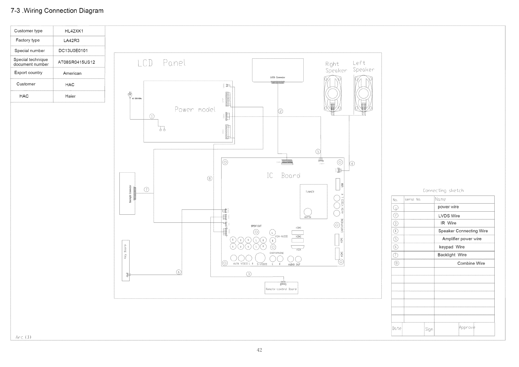
7-3 .Wiring Connection Diagram
Customer type HL42XK1
i \
Factory type LA42R3
Special number DC13UOE0101
Special technique
document number AT08SR0415US12
Export country American
Customer HAC :_
"AC.....................................................................................Ha!::.................................................................
' i
Pov,,,,pp modoi
LVD8Connector
_ ) >01< ?Y"
J
J
Wr
k .;_i
\._ <i
{--7 i
ti_ 0 ;l<P c h
m iserqot i'D
ii power wire
L::J LVDS Wire
_:::_i,_.i_' ...........................................................................................ri.................................................IR Wire
(4_ i i Speaker Connecting Wire
_) i i Amplifier power wire
{o_ i keypad Wire
Backlight Wire
Combine Wire
J
/:we ( 3 )
42
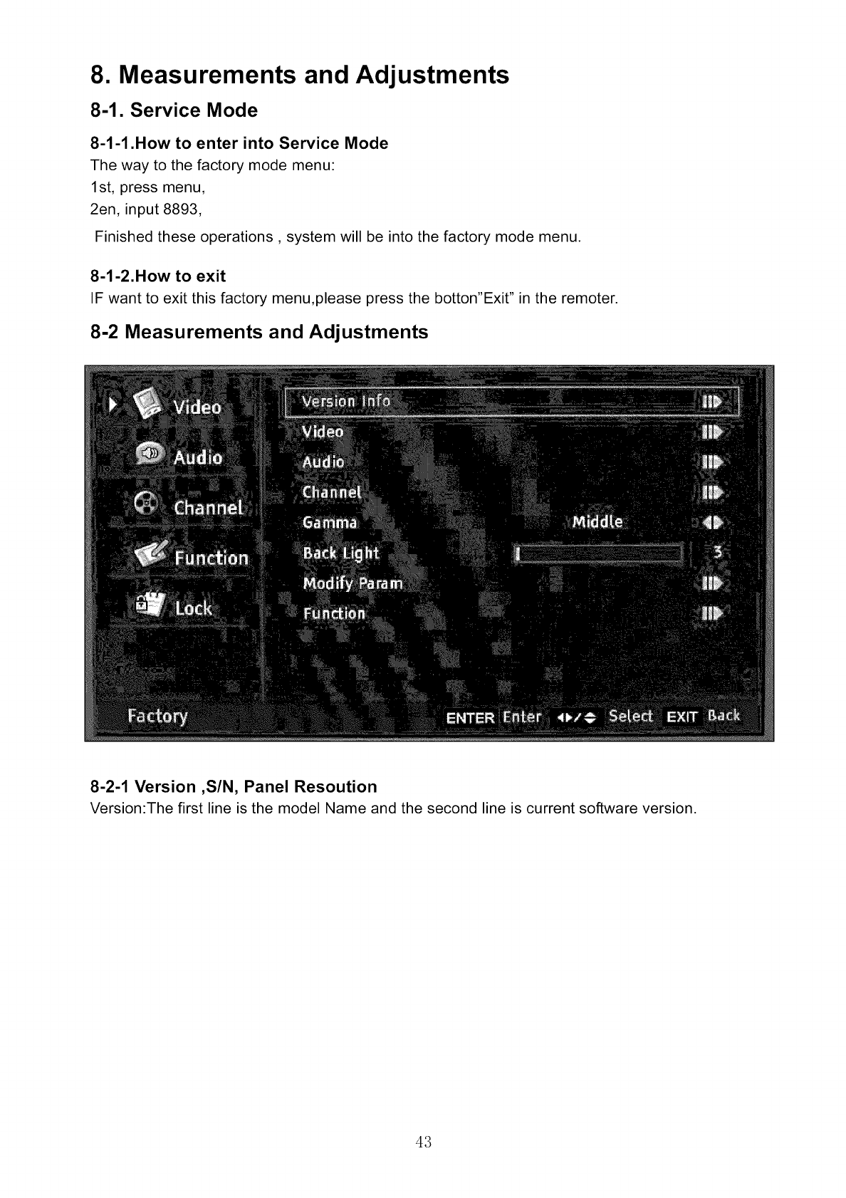
8. Measurements and Adjustments
8-1, Service Mode
8-1-1 .How to enter into Service Mode
The way to the factory mode menu:
1st, press menu,
2en, input 8893,
Finished these operations, system will be into the factory mode menu.
8-1-2.How to exit
IF want to exit this factory menu,please press the botton"Exit" in the remoter.
8-2 Measurements and Adjustments
8-2-1 Version ,S/N, Panel Resoution
Version:The first line is the model Name and the second line is current software version.
43
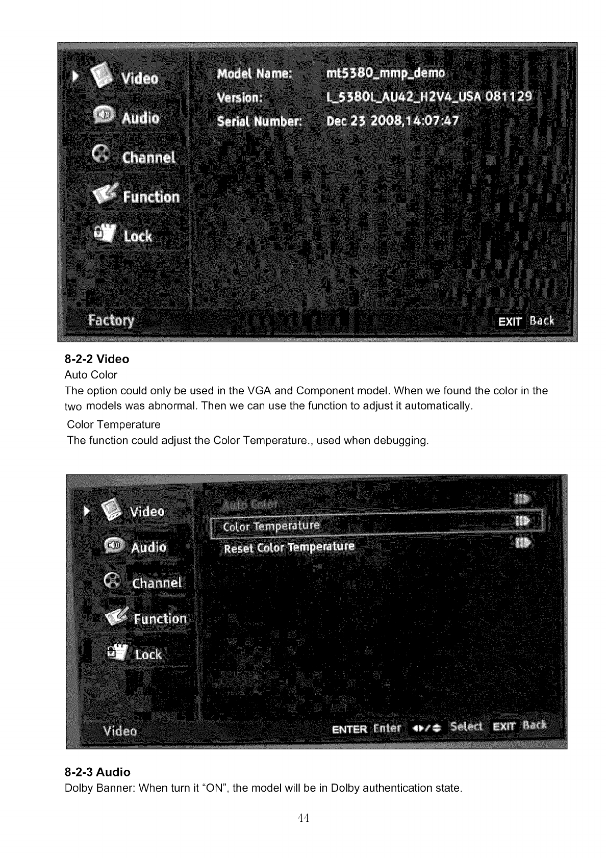
8-2-2 Video
Auto Color
The option could only be used in the VGA and Component model. When we found the color in the
two models was abnormal. Then we can use the function to adjust it automatically.
Color Temperature
The function could adjust the Color Temperature., used when debugging.
8-2-3 Audio
Dolby Banner: When turn it "ON", the model will be in Dolby authentication state.
44
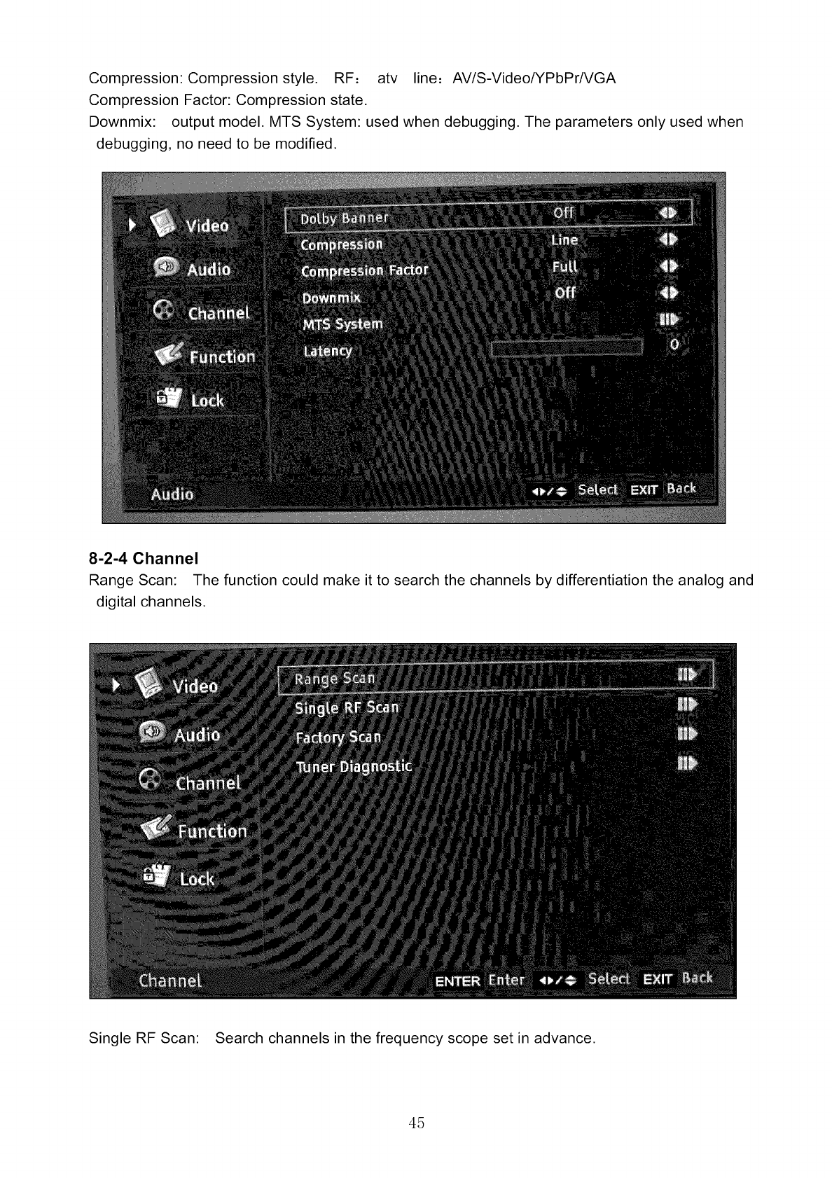
Compression:Compressionstyle. RF: atv line: AV/S-Video/YPbPr/VGA
CompressionFactor:Compressionstate.
Downmix: outputmodel.MTSSystem:usedwhendebugging.The parametersonly usedwhen
debugging,no needto be modified.
8-2-4 Channel
Range Scan: The function could make it to search the channels by differentiation the analog and
digital channels.
Single RF Scan: Search channels in the frequency scope set in advance.
45
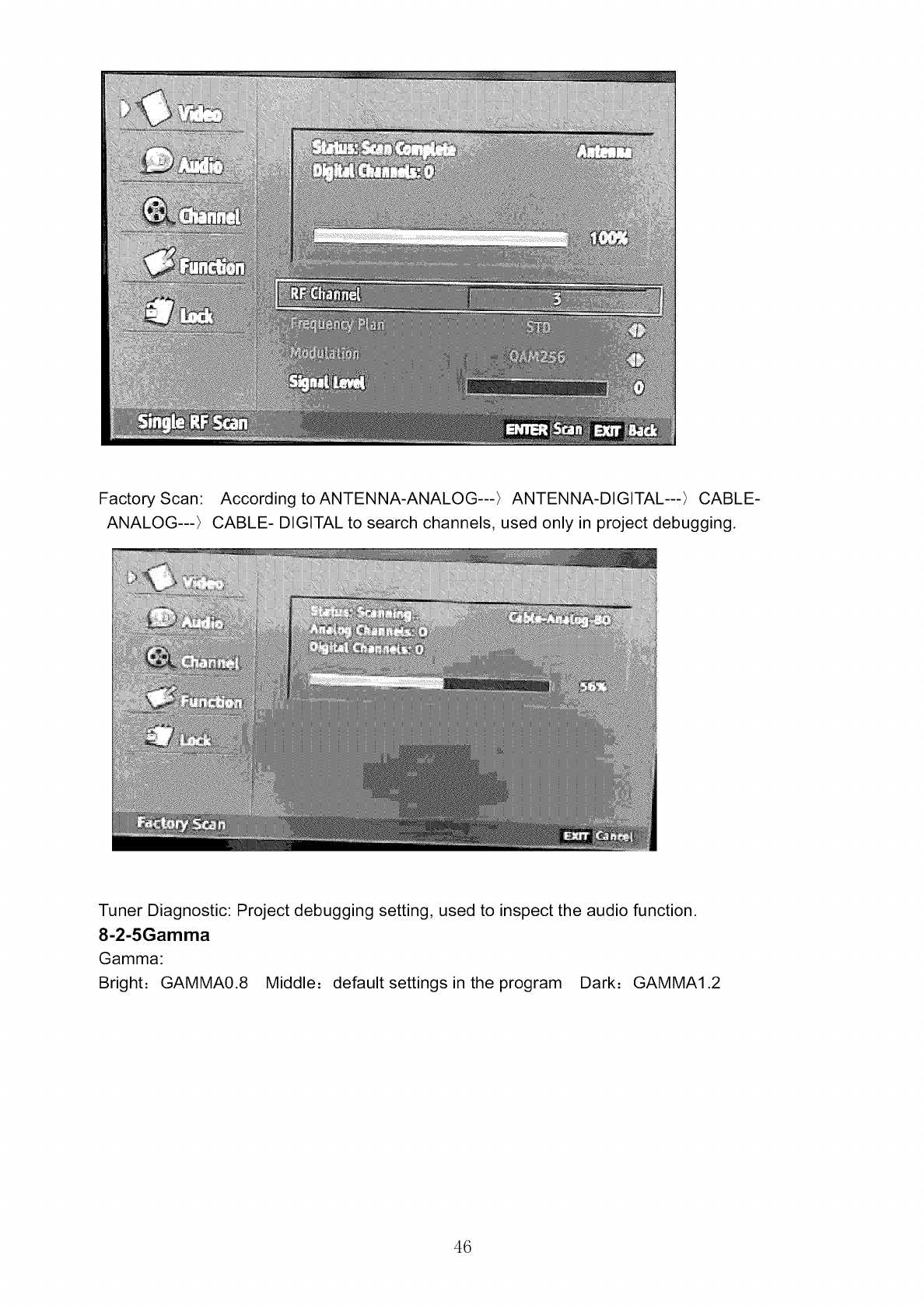
FactoryScan: Accordingto ANTENNA-ANALOG---)ANTENNA-DIGITAL---)CABLE-
ANALOG---) CABLE-DIGITALto searchchannels,usedonlyin projectdebugging.
TunerDiagnostic:Projectdebuggingsetting,usedto inspecttheaudiofunction.
8-2-5Gamma
Gamma:
Bright: GAMMA0.8 Middle: defaultsettingsinthe program Dark: GAMMA1.2
46
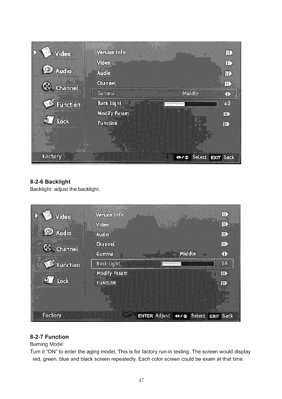
8-2-6 Backlight
Backlight: adjust the backlight.
8-2-7 Function
Burning Mode:
Turn it "ON" to enter the aging model, This is for factory run-in testing. The screen would display
red, green, blue and black screen repeatedly. Each color screen could be exam at that time.
47
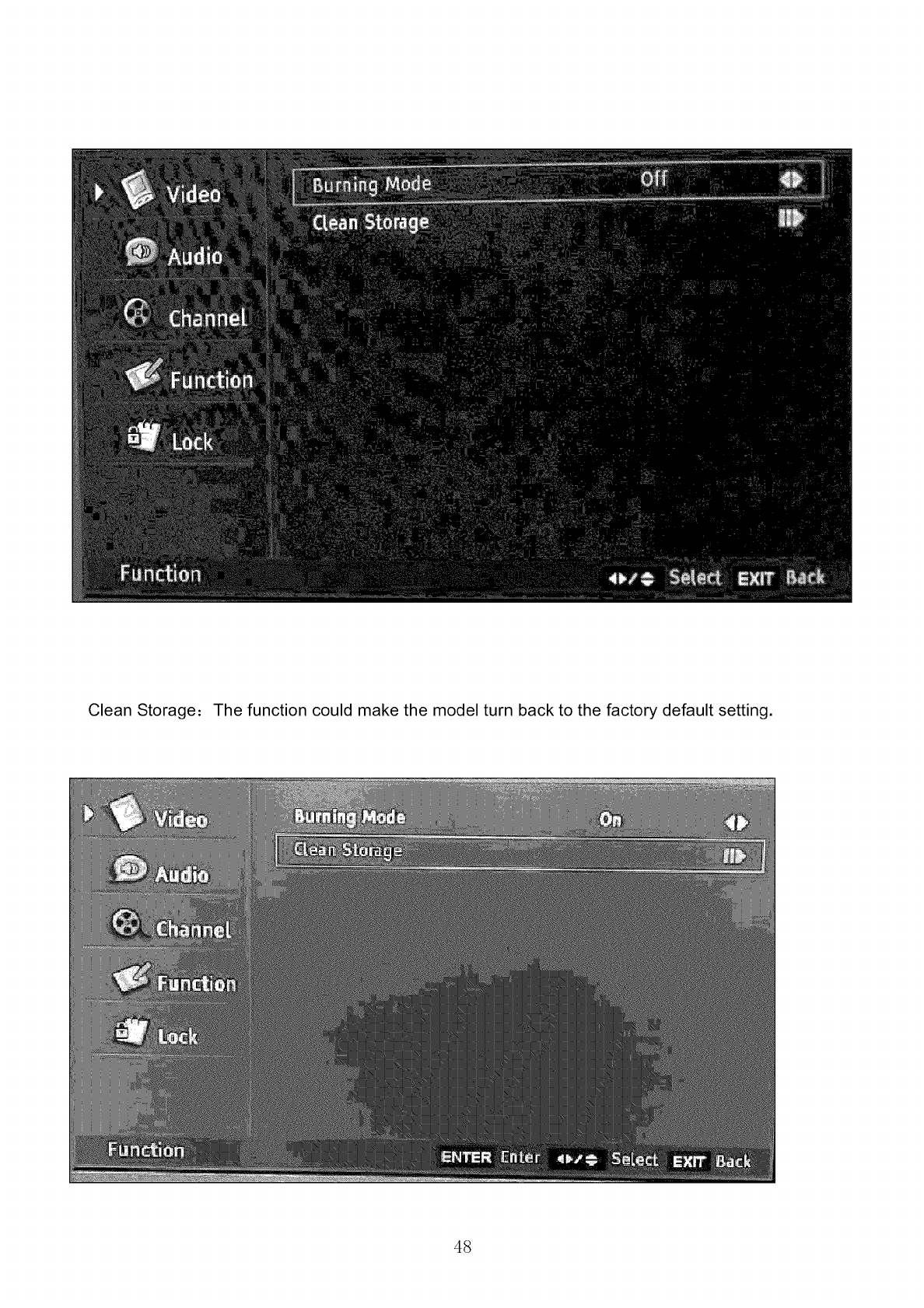
CleanStorage. Thefunctioncouldmakethe modelturnbackto the factorydefaultsetting.
48
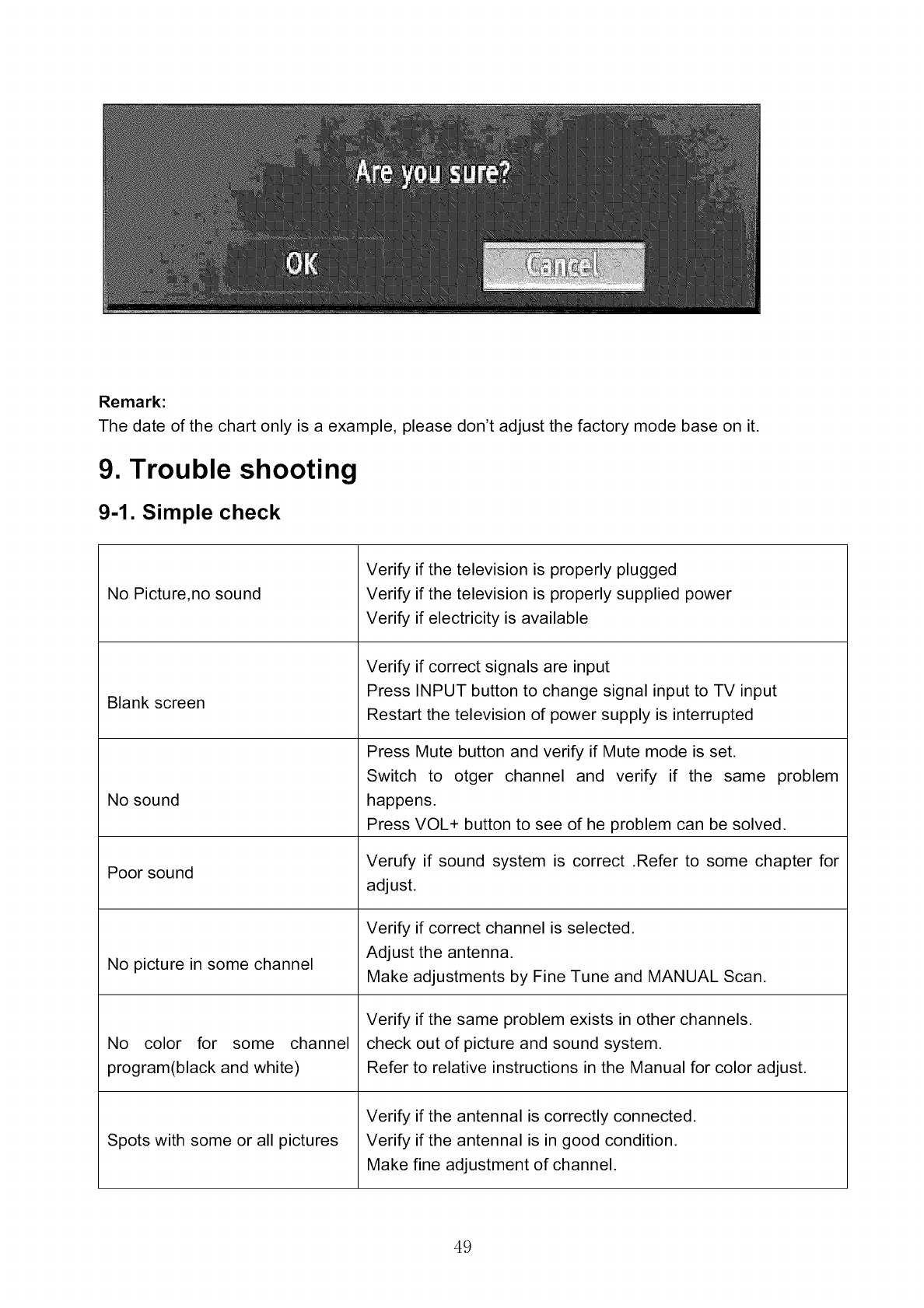
Remark:
Thedateofthe chartonlyis a example,pleasedon'tadjustthefactorymodebaseon it.
9. Trouble shooting
9-1. Simple check
No Picture,no sound
Blank screen
No sound
Poor sound
No picture in some channel
No color for some channel
program(black and white)
Spots with some or all pictures
Verify if the television is properly plugged
Verify if the television is properly supplied power
Verify if electricity is available
Verify if correct signals are input
Press INPUT button to change signal input to TV input
Restart the television of power supply is interrupted
Press Mute button and verify if Mute mode is set.
Switch to otger channel and verify if the same problem
happens.
Press VOL+ button to see of he problem can be solved.
Verufy if sound system is correct .Refer to some chapter for
adjust.
Verify if correct channel is selected.
Adjust the antenna.
Make adjustments by Fine Tune and MANUAL Scan.
Verify if the same problem exists in other channels.
check out of picture and sound system.
Refer to relative instructions in the Manual for color adjust.
Verify if the antennal is correctly connected.
Verify if the antennal is in good condition.
Make fine adjustment of channel.
49
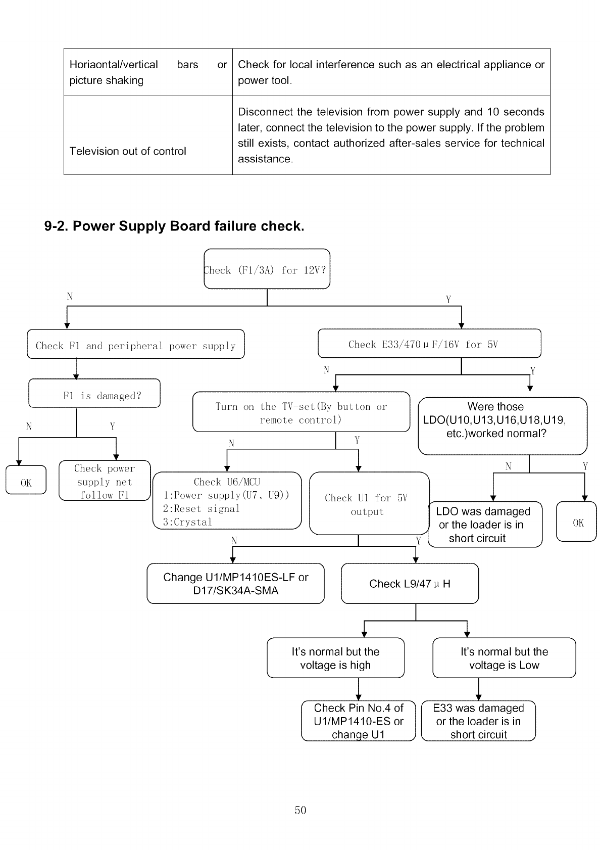
Horiaontal/vertical
pictureshaking
Televisionoutof control
bars or Check for local interference such as an electrical appliance or
power tool.
Disconnect the television from power supply and 10 seconds
later, connect the television to the power supply. If the problem
still exists, contact authorized after-sales service for technical
assistance.
9-2. Power Supply Board failure check.
heck (F1/3A) fo:F 12V'.71
I
N
Check FI and peripheral power supply
F1 is damaged? ] I
N Y
[ Check p!wez"
supp[y net
fol low FI
N
Y
Check E33/470 p F/16V for 5V
Tu:Fn on the TV set(By button o:F
:['emote cont:Fol)
I Y
Check U6/MCU
1'Power supply(U7, U9))
2'Reset signal
3' Crystal x I
Change U1/MP1410ES-LF or
D 17/S K34A-S MA
Check U1 fo:F 5V
output yt
]i check. ,47
I
It's normal but the 1 Ivoltage is high
I CheckPinN°'4°f II
U1/MP1410-ES or
change U1
I]
(Were those 1
I LDO(U10,U13,U16,U18,U19,
_ etc.)worked normal?
_ J Y
LDO was damaged J
or the loader is in
short circuit
It's normal but the
voltage is Low
E33 was damaged "}
or the loader is in J
short circuit
]
50
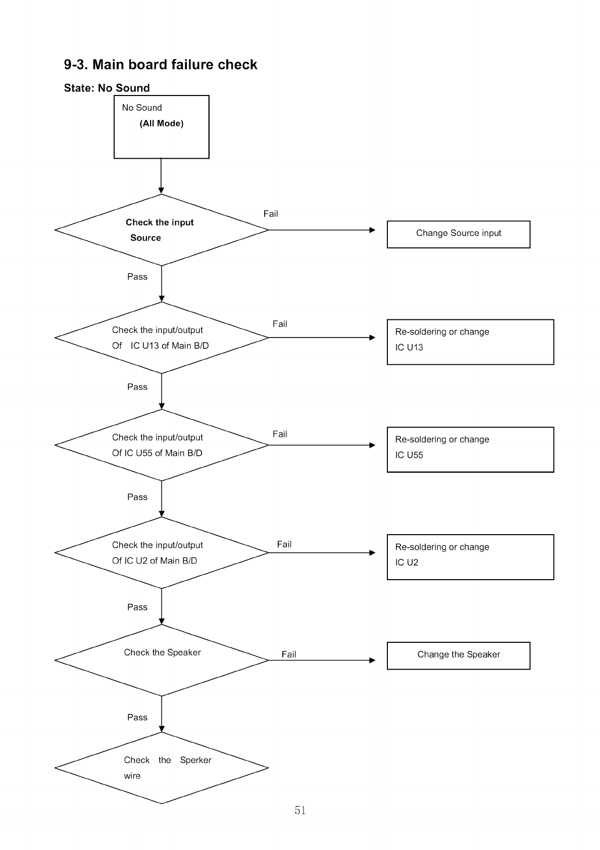
9-3. Main board failure check
State: No Sound
No Sound
(All Mode)
1
ail
_Fail
Fail
Fail
Fail
51
I
I
Change Source input
Re-soldering or change
IC U13
Re-soldering or change
IC U55
Re-soldering or change
IC U2
Change the Speaker
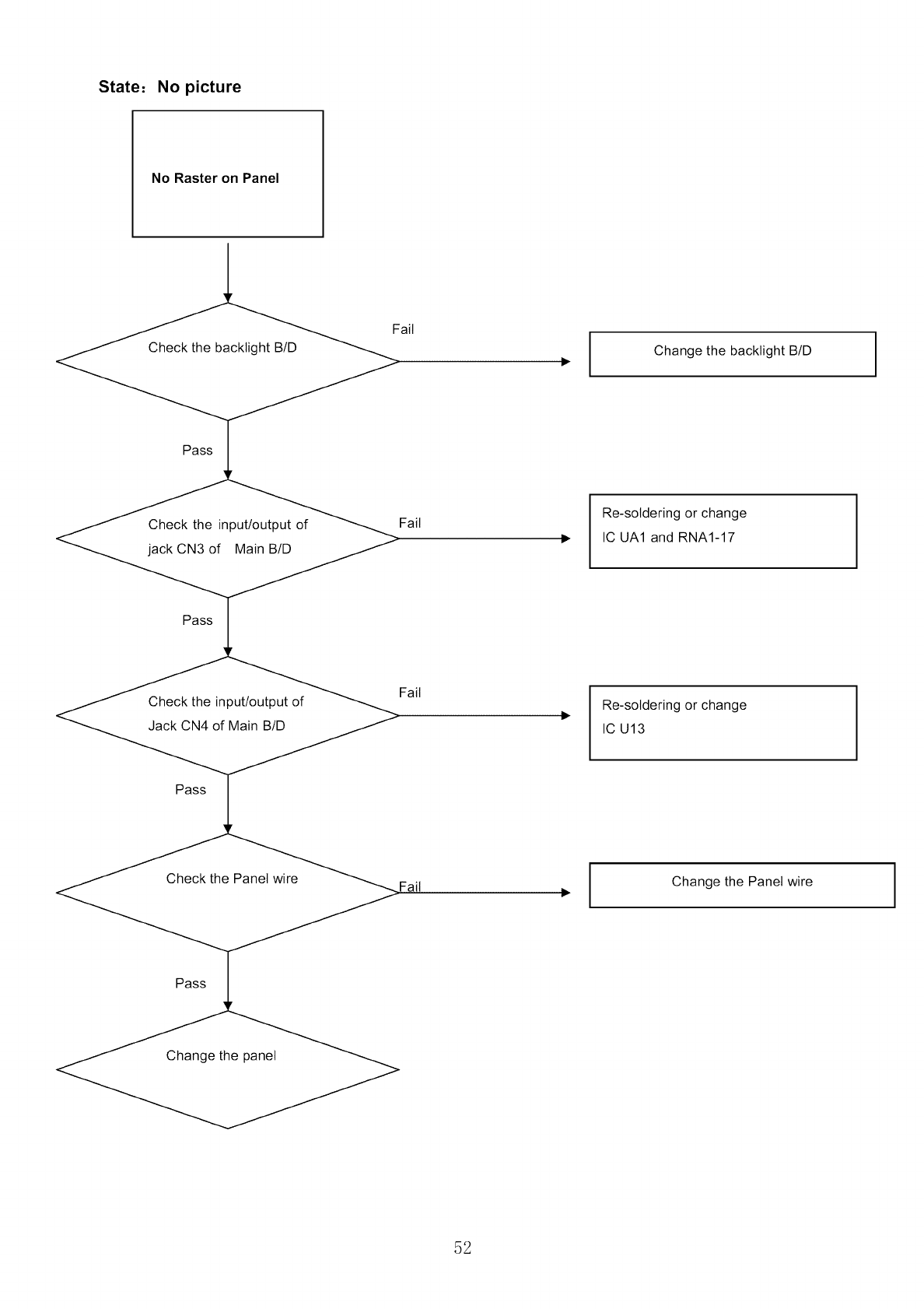
State= No picture
No Raster on Panel
ail
Fail
Fail
Fail
t,.
v
Change the backlight B/D
Re-soldering or change
IC UA1 and RNA1-17
Re-soldering or change
IC U13
Change the Panel wire
I
52
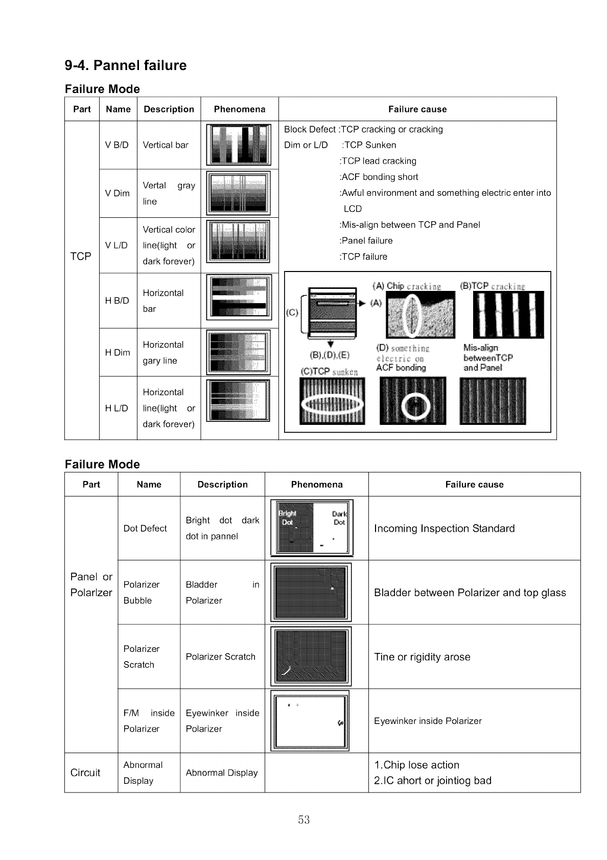
9-4. Pannel failure
Failure Mode
Part
TCP
Name
V B/D
V Dim
V L/D
H B/D
H Dim
H L/D
Description
Vertical bar
Vertat gray
line
Vertical color
line(light or
dark forever)
Horizontal
bar
Horizontal
gary line
Horizontal
line(light or
dark forever)
Failure cause
Block Defect :TCP cracking or cracking
Dim or L/D :TCP Sunken
:TCP lead cracking
:ACF bonding short
:Awful environment and something electric enter into
LCD
:Mis-align between TCP and Panel
:Panel failure
:TCP failure
Phenomena
(C)
ACF bnding _nd P_
Failure Mode
Part Name Description Phenomena Failure cause
Panel or
Polarizer
Dot Defect
Polarizer
Bubble
Polarizer
Scratch
F/M inside
Polarizer
Bright dot dark
dot in pannel
Bladder in
Polarizer
Polarizer Scratch
Eyewinker inside
Polarizer
D_k
Dot Incoming Inspection Standard
Bladder between Polarizer and top glass
Tine or rigidity arose
Eyewinker inside Polarizer
Abnormal 1 .Chip lose action
Circuit Abnormal Display
Display 2.1C ahort or jointiog bad
53
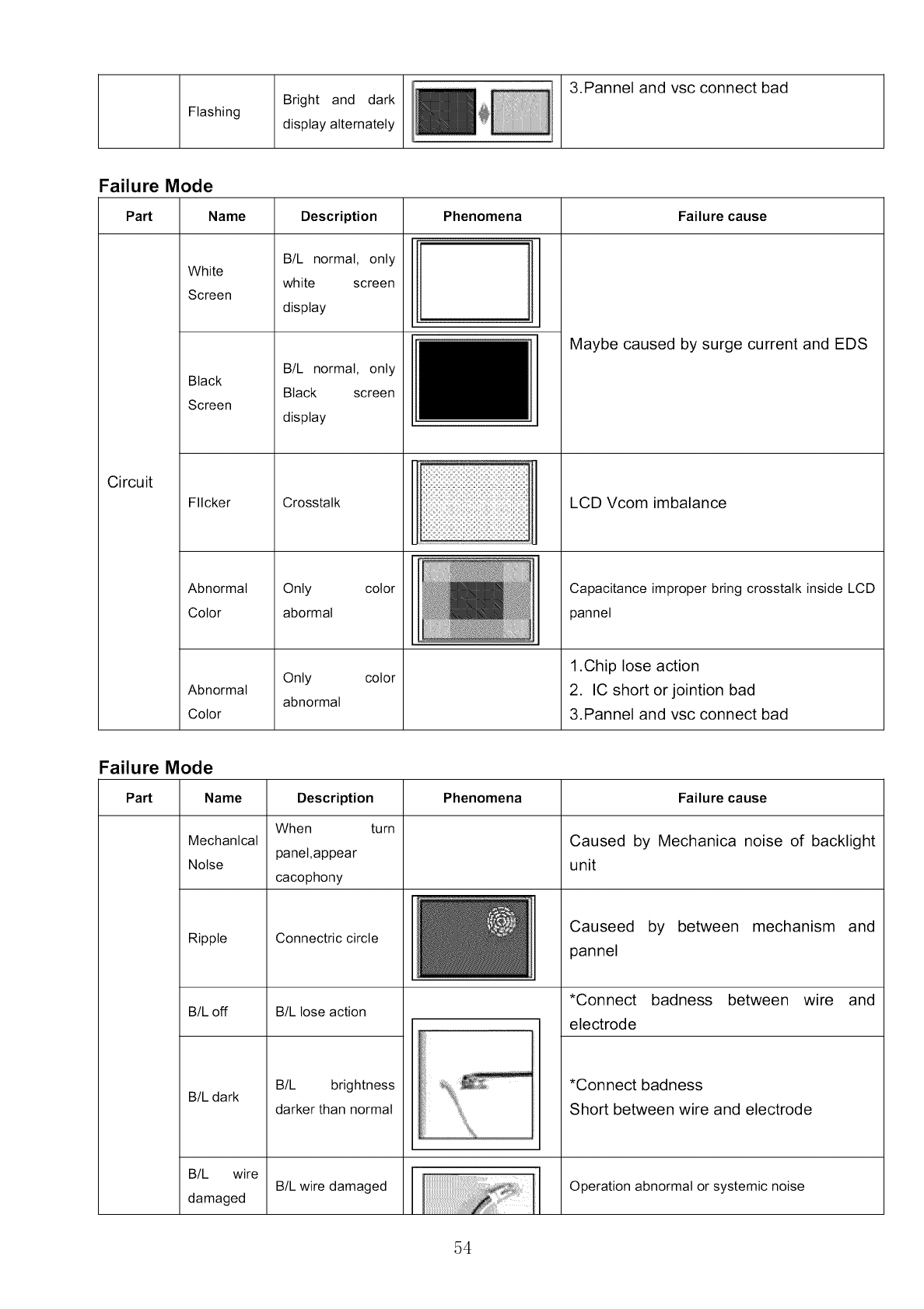
Flashing Bright and dark
display alternately
3.Pannel and vsc connect bad
Failure Mode
Part Name
White
Screen
Black
Screen
Circuit
Flicker
Abnormal
Color
Abnormal
Color
Description
B/L normal, only
white screen
display
B/L normal, only
Black screen
display
Crosstatk
Only color
abormal
Only color
abnormal
Phenomena
!Failure cause
Maybe caused by surge current and EDS
LCD Vcom imbalance
Capacitance improper bring crosstalk inside LCD
pannel
1.Chip lose action
2. IC short or jointion bad
3.Pannel and vsc connect bad
Failure Mode
Part Name Description Phenomena Failure cause
When turn
Mechanical Caused by Mechanica noise of backlight
panel,appear
Noise unit
cacophony
Ripple
B/L off
B/L dark
B/L wire
damaged
Connectric circle
B/L lose action
B/L brightness
darker than normal
B/L wire damaged
Causeed by between mechanism and
pannel
*Connect badness between
electrode
*Connectbadness
Shortbetween wire and electrode
Operation abnormal or systemic noise
wire and
54
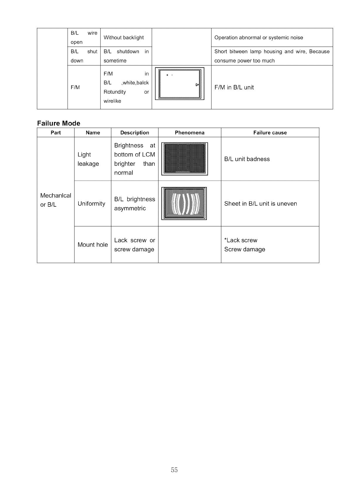
B/L
open
B/L
down
F/M
wire
shut
Without backlight
B/L shutdown
sometime
F/M in
B/L ,white,batck
Rotundity or
wirelike
Operation abnormal or systemic noise
Short bitween lamp housing and wire, Because
consume power too much
F/M in B/L unit
Failure Mode
Part Name Description Phenomena Failure cause
Mechanical
or B/L
Light
leakage
Uniformity
Mount hole
Brightness at
bottom of LCM
brighter than
normal
B/L brightness
asymmetric
Lack screw or
screw damage
B/L unit badness
Sheet in B/L unit is uneven
*Lack screw
Screw damage
55

Sincere Forever
56
