Hangzhou Gubei Electronics Technology 3303-SBSL Wifi Module User Manual
Hangzhou Gubei Electronics Technology Co.,Ltd Wifi Module
User Manual
User Manual
Model:3303-SBSL

Module Features
A. Support IEEE802.11b/g/n wirelessstandards
B. SupportWEP、WPAandWPA2 encryption
C. SupportUART\PWM\ADC\GPIO\I2C Interface
D. Support STA\AP\AP+STA mode,etc.
E. Support a key function Configuration
F.Support TLS\SSL protocol andmDNS
G.Support PCB antenna
H. 3.3Vpower supply
I. Size 17.7mm*31mm*3.6mm(with shield)
1. Product Overview (Hardware)
WT2SBSLadopts MTK IOT scheme , is a support 802.11b/g/nWiFi module is ,can
communicate with other device via UART port。Module integrates RF transceiver ,MAC,
Base-Band , all WIFI protocol and configuration information and network protocol stack , can
be widely used in fields such as intelligent home device , remote monitoring equipment ,
medicine and other fields .
Module integrated ARM Cortex-M4F processor , high primary frequencycan reach
192MHz , SRAM 352KB , and built-in 2MB Flash .
1.1 Module basic parameter
1.1.1 Wlan parameter
Frequency Range 2.412 GHz - 2.462 GHz
Wireless Standard IEEE 802.11 b/g/n
RF Power
Antenna Built-in:PCB antnna
Extenrnal:not support
Receiving Sensitivity
802.11b<-91dBm@1Mbps
802.11b<-81dBm@11Mbps
802.11g<-86dBm@6Mbps
802.11g<-69dBm@54Mbps
Protocol Stack IPv4, TCP/UDP/FTP/HTTP/HTTPS/TLS/mDNS
Data Rate(max)11M@802.11b, 54M@802.11g, MCS7@802.11n
Security Support
Encryption Standard:WEP/WEPA/WPA2
Encryption Algorithm:
WEP64/WEP128/TKIP/AES
Network Type STA/AP/STA+AP/WIFI Direct
802.11 b: 15.2-15.72dBm; 802.11 g:12.36-13.20dBm
802.11 n20: 11.23-12.27dBm; 802.11 n40:9.63-9.71dBm

1.1.2 Absolute Maximum Ratings
Symbol Description Min. Max. Units
Ts Storage temperature -40 125 ℃
TAAmbient operating
temperature
0 70 ℃
Vdd Supply voltage 3.0 3.6 V
Vio Voltage on IO pin 0 3.3 V
ESD ESD protection (HBM) 2000 V
1.1.3 DC Voltage and current
Specifications Min. Typ. Max. Units
VDD 3 3.3 3.6 V
VIL(input low voltage) 0 0.8 V
VIH(input high voltage) 2 3.6 V
VOL(output low voltage) 0 0.4 V
VOH(output high voltage) 2.4 3.6 V
Io 4 16 mA
RPU (Pullup Resistance) 40 190 kΩ
RPD(Pulldown Resistance) 10 50 kΩ
Standby 110 mA
pulse current @TX
11b @18dBm 11Mbps
320 335 mA
pulse current @TX
11g @16dBm 54Mbps
280 290 mA
1.1.4 IEEE802.11b mode
ITEM Specification
Modulation Type DSSS / CCK
Frequency range 2412MHz~2462MHz
Channel CH1 to CH11
Data rate 1, 2, 5.5, 11Mbps
TX Characteristics Min Typical Max. Unit
Transmitter Output Power
11bTarget Power 16 dBm
Frequency Error -10 +10 ppm
Constellation Error( peak EVM)@ target power
1~11Mbps -40
RX Characteristics Min Typical Max. Unit

Minimum Input Level Sensitivity
1Mbps (FER≦8%) -94 -91 dBm
11Mbps (FER≦8%) -84 -81 dBm
Maximum Input Level
(FER≦8%)
-10 dBm
1.1.5 IEEE802.11g mode
ITEM Specification
Modulation Type OFDM
Frequency range 2412MHz~2462MHz
Channel CH1 to CH11
Data rate 6, 9, 12, 18, 24, 36, 48, 54Mbps
TX Characteristics Min Typical Max. Unit
Transmitter Output Power
11gTarget Power 13.5 dBm
Frequency Error -10 +10 ppm
Constellation Error( peak EVM)@ target power
6Mbps -26 dB
54Mbps -33 dB
Transmit spectrum mask
@11MHz -20 dBr
@20MHz -28 dBr
@30MHz -40 dBr
RX Characteristics Min Typical Max. Unit
Minimum Input Level Sensitivity
6Mbps -90 -86 dBm
54Mbps -71 -69 dBm
Maximum Input Level
(FER≦10%)
-20 dBm

1.1.6 IEEE802.11n 40MHz bandwidth mode
ITEM Specification
Modulation Type OFDM
Frequency range 2422MHz~2452MHz
Channel CH3 to CH11
Data rate MCS0/1/2/3/4/5/6/7
TX Characteristics Min Typical Max. Unit
Transmitter Output Power
11n HT40 Target Power 10 dBm
Frequency Error -10 +10 ppm
Constellation Error( peak EVM)@ target power
MCS0 -26 dB
MCS7 -33 dB
Transmit spectrum mask
@11MHz -20 dBr
@20MHz -28 dBr
@30MHz -40 dBr
RX Characteristics Min Typical Max. Unit
Minimum Input Level Sensitivity
MCS0 -90 -86 dBm
MCS7 -71 -69 dBm
Maximum Input Level
(FER≦10%)
-20 dBm

1.1.6 IEEE802.11n 20MHz bandwidth mode
ITEM Specification
Modulation Type OFDM
Frequency range 2412MHz~2462MHz
Channel CH1 to CH11
Data rate MCS0/1/2/3/4/5/6/7
TX Characteristics Min Typical Max. Unit
Transmitter Output Power
11n HT20 Target Power 12.5 dBm
Frequency Error -10 +10 ppm
Constellation Error( peak EVM)@ target power
MCS0 -26 dB
MCS7 -33 dB
Transmit spectrum mask
@11MHz -20 dBr
@20MHz -28 dBr
@30MHz -40 dBr
RX Characteristics Min Typical Max. Unit
Minimum Input Level Sensitivity
MCS0 -90 -86 dBm
MCS7 -71 -69 dBm
Maximum Input Level
(FER≦10%)
-20 dBm

IEEE802.11n 40MHz bandwidth mode
ITEM Specification
Modulation Type OFDM
Frequency range 2422MHz~2452MHz
Channel CH3 to CH9
Data rate MCS0/1/2/3/4/5/6/7
TX Characteristics Min Typical Max. Unit
Transmitter Output Power
11n HT40 Target Power 10 dBm
Frequency Error -10 +10 ppm
Constellation Error( peak EVM)@ target power
MCS0 -26 dB
MCS7 -33 dB
Transmit spectrum mask
@11MHz -20 dBr
@20MHz -28 dBr
@30MHz -40 dBr
RX Characteristics Min Typical Max. Unit
Minimum Input Level Sensitivity
MCS0 -90 -86 dBm
MCS7 -71 -69 dBm
Maximum Input Level
(FER≦10%)
-20 dBm
1.1.7
1.2 Hardware Description
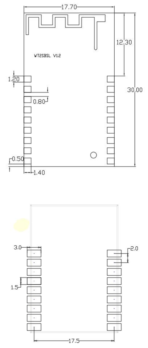
1.2.1 Mechanical Dimensions
1.2.2 Recommend package dimension
(unit:mm)
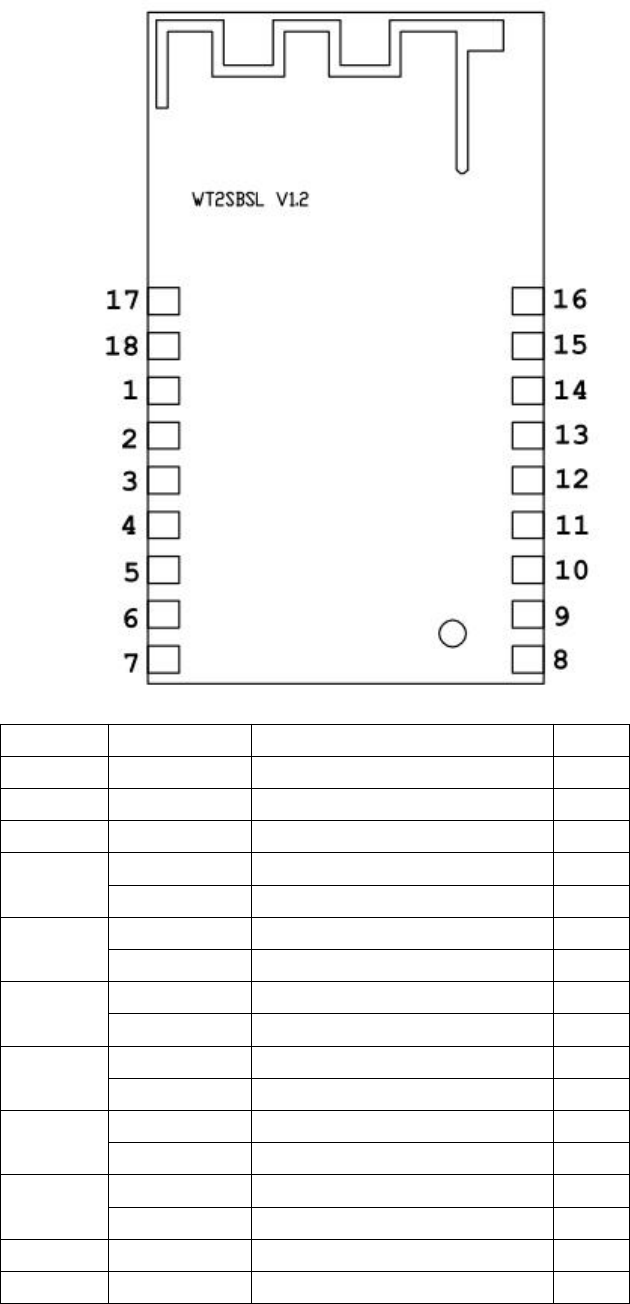
1.2.3Interface definition
pin
net
description
type
1
GND
GND
POWER
2
VDD
3.3V
POWER
3
NRST
Hardware reset(restart)
I
4
TX0
UART0 TX
O
GPIO3
I/O
5
RX0
UART0 RX
I
GPIO2
I/O
6
TX1
UART1 TX
O
GPIO37
I/O
7
RX1
UART1 RX
I
GPIO36
I/O
8
RX1
UART1 RX
I
GPIO36
I/O
9
TX1
UART1 TX
O
GPIO37
I/O
10
GPIO39
I/O
11
GPIO35
I/O

12
GPIO33
I/O
13
VDD
3.3V
POWER
14
GND
GND
POWER
15
GPIO57
I/O
ADC_IN0
ADC Input0
I
16
GPIO58
I/O
ADC_IN1
ADC Input1
I
17
I2C1_SCL
I/O
GPIO24
I/O
18
I2C1_SDA
I/O
GPIO25
I/O
Note:
1. UART 0 is used for general transparent transmission , and UART1 is used for the
output of debug information,and the serial ports output level is described with
reference to DC characteristics,by default.
2. NRST is that module hardware resets ,and low level is effective ,restars after
module resets,adn keeps original configuration information. The inner existing
RC electrify restoration circuit of module itself.
3. Under the default situations,PIN 12 (GPIO33) is the network light pin,is used for
external LED,the configuring condition of indicating module.
4. Under the default situations,PIN11 (GPIO35) is the module software reset pin,and
high level is effective,and former configuration information of the back module
that resets is eliminated similar factory reset.
5. All GPIO all support PWM output.
6. TX and RX are used for communicating with the ppu of 3V power supply among
the UART0,and the serial ports output level is described with reference to
3.3joint DC characteristics.
7. Unsettled processing is done in the GPIO suggestion that is not used,and forbids
on the circuit that to GPIO35,GPIO37 does and draws processing.
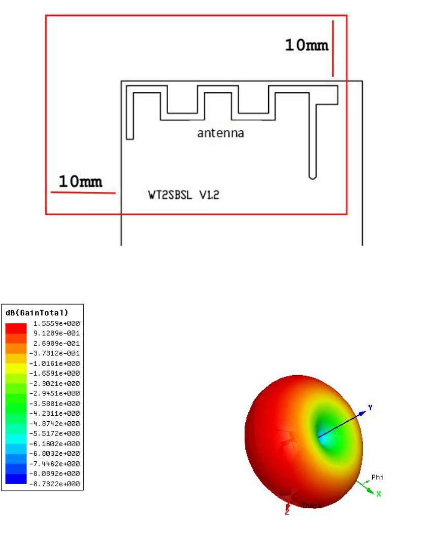
1.2.3 Built-in Antenna
The support of this module selects PCB board to carry antenna,and in 2.4G~2.5G
frequency range,antenna port S11 is less than -10dB,the about 1.5dB of antenna gain.
antnna gain emulation rediation diagram
The antnna port S11simulation curve
When selecting the PCB antnna,the module in place should pay attention to the
following points when :
1. Components and parts and floor files can not be placed in user PCB base plate and
module antenna corresponding region,preferably can be with PCB hollow out that
should the zone.
2. Do not place any components and parts in the suggestion module antenna area
10mm,the module base plate is also avoided cabling as for as possible in this
zone,forbids applying copper
3. Use in the mould that module is not placed on metal-back or has metal to spray
paint.
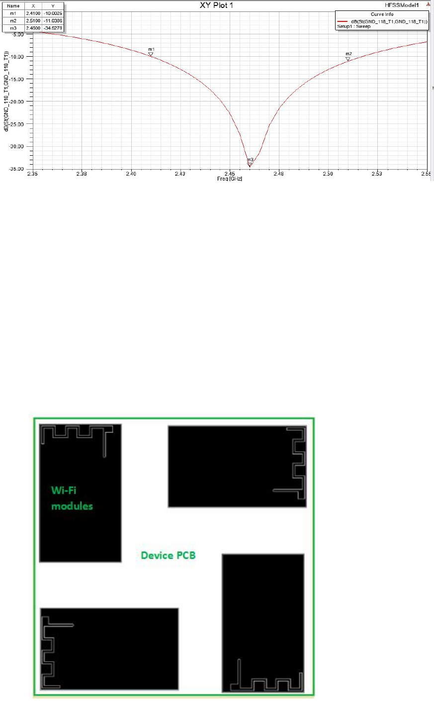
4. The user is when the pcb board layout in suggestion,as far as possible with the
antnna of wifi module near bottom edge,be shown in the following figure,to
guarantee the good performance of antnna.
1.3The Hardware Reference Design
1.3.1 The UART Interface Design
For the equipment of 3.3V power supply,can equipment of serial and module serial
ports directly be linked to each other by the diagram circuit and accomplish
communication;
If the 5V power supply unit can or design the associated level change-over circuit
voluntarity with reference to following circuit,resistance value can be adjusted
according to side circuit.
1.3.2 Power Reguirements
Give module for power supply if produce 3.3V voltage through LDO, then the
capacitance of C1 can be considered with 10u ~ 22u;Give module for power supply if
produce 3.3V through the DCDC power supply, the electric capacity of C1 can be
considered with 47u or bigger alminium electrolytic condenser。
Please guarantee that power supply can provide enough big electric current, power
down occur to avoid module when sending data, the maximum input current of
suggestion module is greater than 330mA
Module leaves two 3.3Vpin, both can select a pin to module voltage to be provided
arbitrarily, also can supply power simultaneously by two pin

Maintenance
1.Power rating: Input DC3.3V
2.Declaration of Conformity
Hangzhou Gubei Electronics Technology Co., Ltd. hereby declares that this Wifi
Module is in compliance with the essential requirements and other relevant provisions
of Directive 1999/5/EC.a copy of the original declaration of conformity may be found or
obtained at https://shop1413998575180.1688.com/
FCC Caution.
This device complies with part 15 of the FCC Rules. Operation is subject to the
following two conditions: (1) This device may not cause harmful interference, and (2)
this device must accept any interference received, including interference that may
cause undesired operation.
Any Changes or modifications not expressly approved by the party responsible for
compliance could void the user's authority to operate the equipment.
Note: This equipment has been tested and found to comply with the limits for a Class B
digital device, pursuant to part 15 of the FCC Rules. These limits are designed to
provide reasonable protection against harmful interference in a residential installation.
This equipment generates uses and can radiate radio frequency energy and, if not
installed and used in accordance with the instructions, may cause harmful interference
to radio communications. However, there is no guarantee that interference will not
occur in a particular installation. If this equipment does cause harmful interference to
radio or television reception, which can be determined by turning the equipment off
and on, the user is encouraged to try to correct the interference by one or more of the
following measures:
-Reorient or relocate the receiving antenna.
-Increase the separation between the equipment and receiver.
-Connect the equipment into an outlet on a circuit different from that to which the
receiver is connected.
-Consult the dealer or an experienced radio/TV technician for help.
The distance between user and device should be no less than 20cm.
The Wifi module is designed to comply with the FCC statement. FCC ID is
2ACDZ-3303-SBSL. The host system using Wifi module, should have label
indicated it contain modular FCC ID: 2ACDZ-3303-SBSL