Hetronic RXMFS-AC16R RX_MFS-AC16 User Manual RX MFS AC16R User s Manual Rev 5
Hetronic International Inc RX_MFS-AC16 RX MFS AC16R User s Manual Rev 5
Hetronic >
Users Manual Rev 5

User’s Manual
RX_MFS-AC16R

Research and Development
Technical Documentation
Revision Project: Page
5 Description: RX_MFS-AC16R 2 of 14
1. TABLE OF CONTENTS
1.TABLE OF CONTENTS ................................................................................................................................ 2
2.CPU PROJECT DESCRIPTION .................................................................................................................... 3
3.CPU TECHNICAL SPECIFICATION ........................................................................................................... 4
4.CPU CONNECTION DIAGRAM .................................................................................................................. 5
5.CPU ASSEMBLY DESCRIPTION ................................................................................................................ 6
6.PWR PROJECT DESCRIPTION .................................................................................................................... 9
7.PWR TECHNICAL SPECIFICATION ........................................................................................................ 10
8.PWR CONNECTION DIAGRAM ............................................................................................................... 11
9.PWR ASSEMBLY DESCRIPTION ............................................................................................................. 12

Research and Development
Technical Documentation
Revision Project: Page
5 Description: RX_MFS-AC16R 3 of 14
2. CPU PROJECT DESCRIPTION
RX_MFS-AC16_CPU is a 2.4GHz Receiver / Controller board with 15 programmable output channels.
Two Controllers are used for Redundant Main Contact cross-checking with dedicated DK31 outputs for
enhanced Safety. Two isolated digital inputs are provided for monitoring external processes. Can be
stacked with a RX MFS-AC16R PWR board to make a complete receiver. Fits the CHR-2 housing.
The RX_MFS-AC16-2G4 uses a 2.4GHz transceiver for RF reception and transmission. The transceiver
uses OQPSK-DSSS modulation. The 2 operation channels (primary and secondary) can be set to 2 of 16
available channels. Additionally, this unit always sends a feedback telegram upon data reception.
The RX_MFS-AC16-2G4 includes a repeater option which can be used to extend the operation range of
a complete 2.4GHz remote control system. This option can only be enabled via H-Link.
All programmable options are configurable by 2.4GHz equipped H-Link units.
FCC ID: LW9-RXMFS-AC16R
IC ID: 2119B-RXMFSAC16R
Note: Operation is subject to the following two conditions: (1) this device may not cause interference,
and (2) this device must accept any interference, including interference that may cause undesired
operation of the device.
Note: The user is cautioned that changes or modifications not expressly approved by the party
responsible for compliance could void the user’s authority to operate the equipment.
Note: The antenna(s) used for this transmitter must be installed to provide a separation distance of at
least 20cm from all persons. The antenna(s) used for this transmitter must not transmit
simultaneously with any other antenna or transmitter, except in accordance with FCC and IC multi-
transmitter product procedures.
Remarque : L'opération est soumis à deux conditions suivantes: (1) ce dispositif ne peut pas causer de
brouillage, et (2) ce dispositif doit accepter toute interférence, y compris le brouillage qui peut causer
intempestif de fonctionnement du dispositif.
Remarque : L'utilisateur est averti que les changements ou modifications non expressément
approuvées par la partie responsable de la conformité pouvaient annuler l'autorisation l'utilisateur à
faire fonctionner l'équipement.
Remarque : L'utilisation utilisée pour cet émetteur doit être installée pour fournir une distance de
séparation d'au moins 20 cm de toutes les personnes. L'utilisation utilisée pour cet émetteur ne doit
pas transmettre simultanément avec une autre antenne ou émetteur, sauf conformément aux
procédures de produits multi-transmitter de FAC et IC.
Research and Development
Technical Documentation
Revision Project: Page
5 Description: RX_MFS-AC16R 4 of 14
3. CPU TECHNICAL SPECIFICATION
Temperature Range -25o to +70o Celsius
Supply Voltage Range 6 to 14Vdc
Supply Current <90mA at 12Vdc input
Outputs RF: Feedback/H-Link Data
15 Digital Outputs
2 DK 32 Logic Level
2 DK31 Open-Collector
Buzzer: Open-Collector 50mA to Vcc
Inputs RF: Control/H-Link Data
ISO Digital - Common to Input1 or Input2: 8 to 240Vdc, 20 to 240Vac
ISO Digital (Common1 LV to Input1 LV) 1 to 5Vdc
ISO Digital (Common2 LV to Input2 LV) 1 to 5Vdc
NOT ISO Analog (Ground to Analog IN1 or Analog IN2) 0 to 5Vdc
Jumpers J1 through J4: Custom configurations.
J5 Open (default): Closed = un-modulated R.F. Transmit Test Mode
J5 and J1 closed for modulated R.F. Transmit Test Mode
J5 and J1 and J2 closed for R.F. Receive Test Mode
Research and Development
Technical Documentation
Revision Project: Page
5 Description: RX_MFS-AC16R 5 of 14
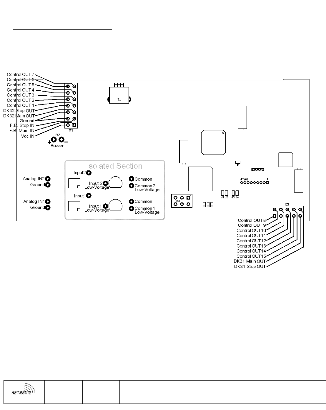
4. CPU CONNECTION DIAGRAM
The following items may be omitted or expanded upon as required.
4.1. Internal Connections
Research and Development
Technical Documentation
Revision Project: Page
5 Description: RX_MFS-AC16R 6 of 14
5. CPU ASSEMBLY DESCRIPTION
5.1. Test / Programming Jumper Configuration
J5 closed for un-modulated R.F. Transmit test mode
J5 and J1 closed for modulated R.F. Transmit test mode
J5 and J1 and J2 closed for R.F. Receive test mode.
5.2. Operational Jumper Configuration
All Jumpers Open = Default
J1 through J4 allow for custom configurations.
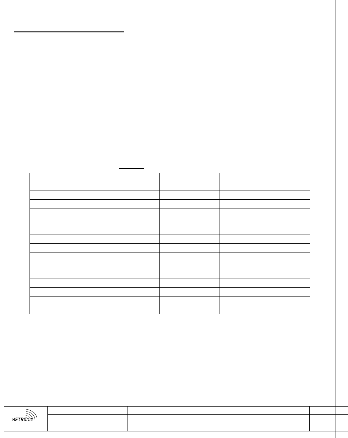
5.3. Wiring
Default wiring configuration includes Buzzer.
Default wiring configuration does not include connections to Digital Inputs.
Function Pad Name Connector Pin-out
Buzzer Positive BZ + Internal
Buzzer Negative BZ - Internal
Digi. IN Common W2A and W2B 22 Isolated- Pads are connected
Digi. IN 1 W1 23 Isolated
Digi. IN 2 W3 24 Isolated
Digi. IN 1 LV Common W5 option Isolated
Digi. IN 2 LV Common W7 option Isolated
Digi IN 1 LV W4 option Isolated
Digi IN 2 LV W6 option Isolated
Analog IN 1 W9 option Warning!! Not isolated
Analog IN 1 Ground W10 option Warning!! Not isolated
Analog IN 2 W11 option Warning!! Not isolated
Analog IN 2 Ground W12 option Warning!! Not isolated
Research and Development
Technical Documentation
Revision Project: Page
5 Description: RX_MFS-AC16R 7 of 14
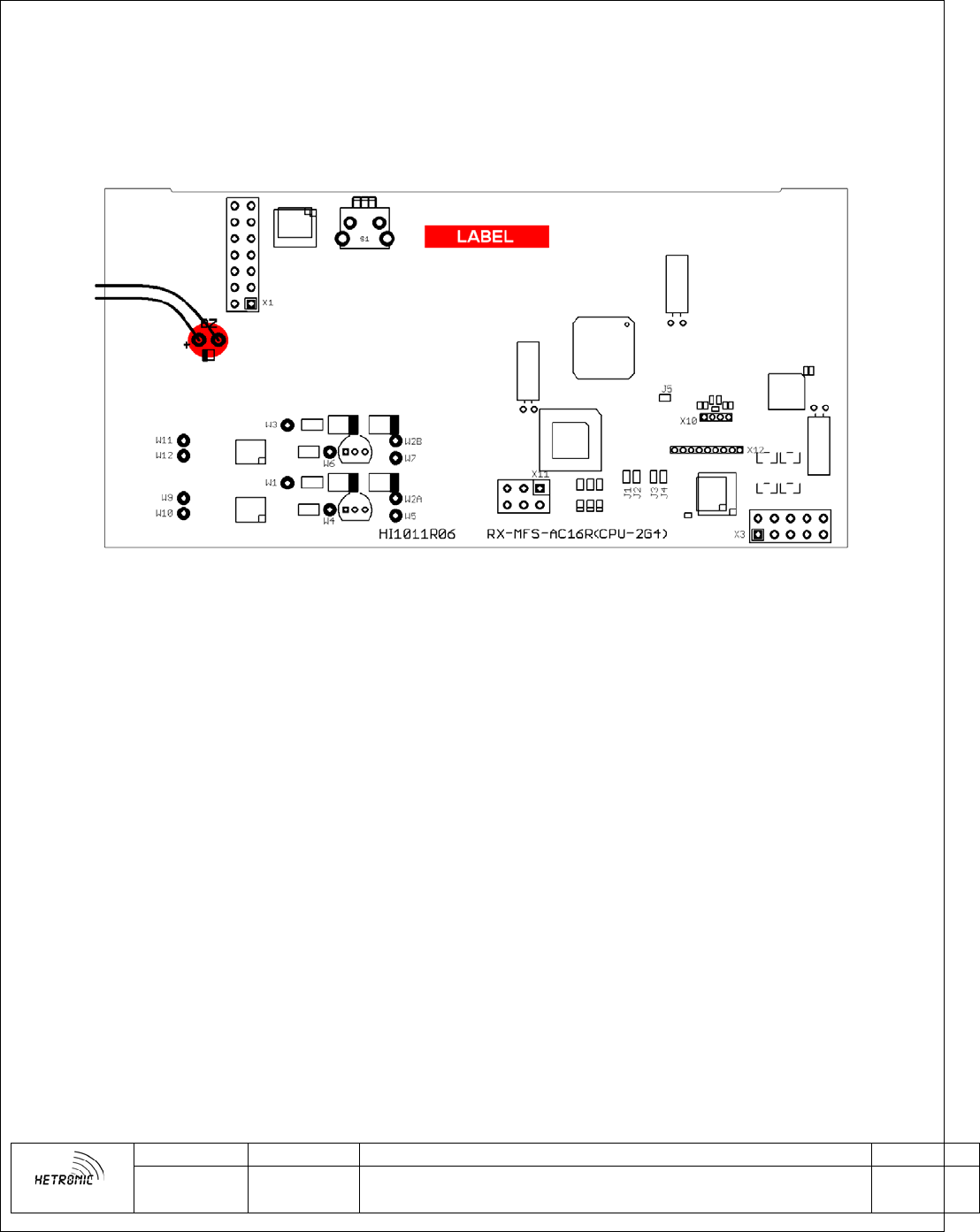
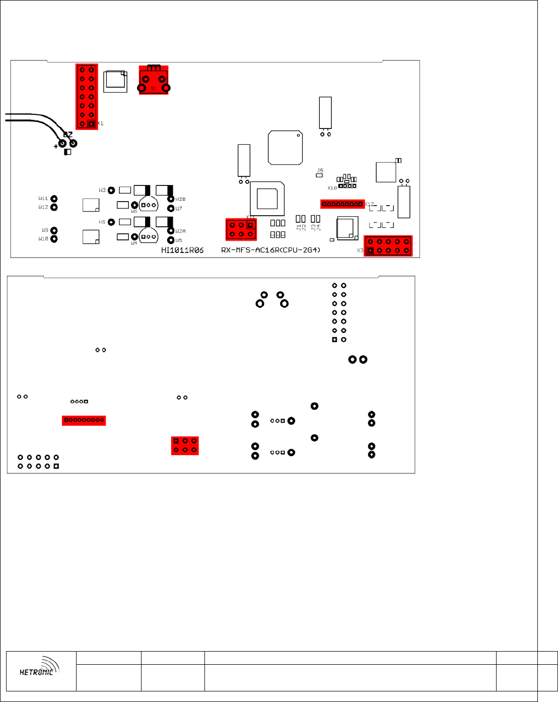
5.4. Glue and Lacquer Masks
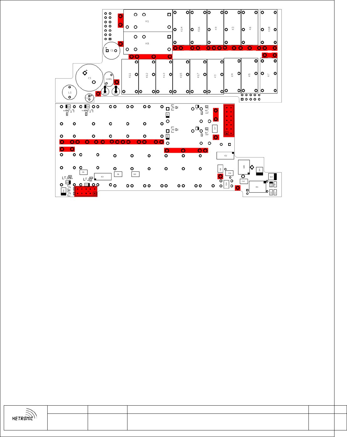
Glue Placement:
Glue Horn wires to CPU board as shown.
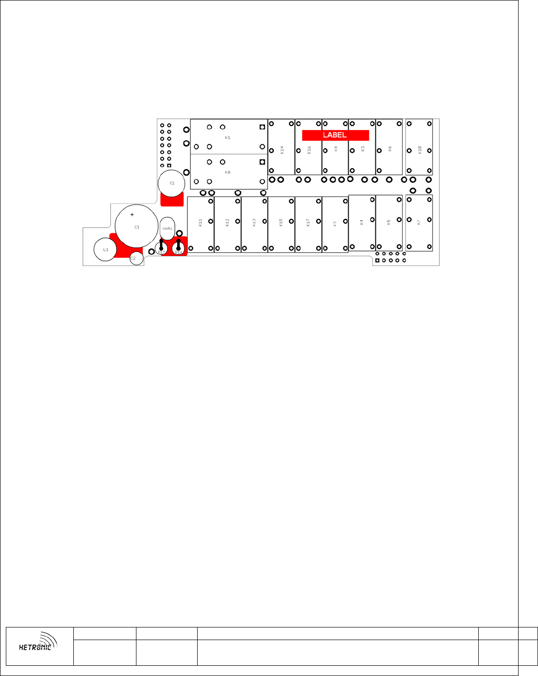
Label Placement:
Place label as shown.
Research and Development
Technical Documentation
Revision Project: Page
5 Description: RX_MFS-AC16R 8 of 14
Lacquer Mask:
Cover the marked areas of the board assembly before lacquering.
Use only Hetronic approved lacquer.

Research and Development
Technical Documentation
Revision Project: Page
5 Description: RX_MFS-AC16R 9 of 14
6. PWR PROJECT DESCRIPTION
RX_MFS-AC16_PWR is a Relay Board with 16 Outputs. Includes two Safety Relays with feedback
signals for redundant, cross-checking Main Contacts, 13 SPST relays and two DPST relays. Coil supply
voltage is switched using AND logic. RX_MFS-AC16_PWR can be stacked with a RX MFS-AC16R
CPU control board to make a complete receiver. Fits CHR-2 housing.
Research and Development
Technical Documentation
Revision Project: Page
5 Description: RX_MFS-AC16R 10 of 14
7. PWR TECHNICAL SPECIFICATION
Temperature Range -25o to +70o Celsius
Supply Voltage Range 40-240 VAC
Power Supply 10.5Vdc ±20%
Jumpers J1,2 Fuse Bypass (default open)
J3 DK32 Combined (default closed)
Outputs Vdd = Supply for Relay Coils and CPU board
15 Relay Outputs (5A max each)
Two Main Contact (8A Max) with available break-out connection.
Main Contact Feedback signals for each Safety Relay
Inputs Two DK32 – Switched High from Logic
Two DK31 – Switched Low from Open-Collector
UB1: for Outputs 1 through 8, 40-240 VAC
UB2: for Outputs 9 through 11, 40-240 VAC
UB3: for Outputs 12 through 15, 40-240 VAC
Research and Development
Technical Documentation
Revision Project: Page
5 Description: RX_MFS-AC16R 11 of 14
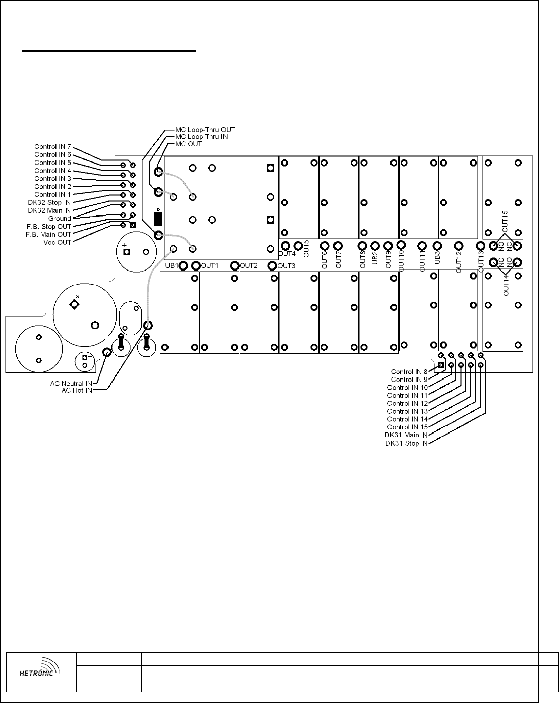
8. PWR CONNECTION DIAGRAM
8.1. Internal Connections
Research and Development
Technical Documentation
Revision Project: Page
5 Description: RX_MFS-AC16R 12 of 14
9. PWR ASSEMBLY DESCRIPTION
9.1. Operational Jumper Configuration
J3 Closed = Default
J3 Open = Combined DK32 Switched Output enable.
9.2. Wiring
Function Pad Name Connector Pinout
AC IN (N) W1 1
AC IN (L1) W2 2
MC OUT W3 3
UB1 W4 4
K1 W5 5
K2 W6 6
K3 W7 7
K4 W8 8
K5 W9 9
K6 W10 10
K7 W11 11
K8 W12 12
UB2 W13 13
K9 W14 14
K10 W15 15
K11 W16 16
UB3 W17 17
K12 W18 18
K13 W19 19
K14 N.O. W20 20
K15 N.O. W21 21
MC Loop-Thru W22 Internal or Break-Out
MC Loop-Thru W22A Internal or Break-Out
Digi. IN Common CPU Brd. 22
Digi. IN1 CPU Brd. 23
K14 N.C. W20A option
Digi. IN 2 CPU Brd. 24
K15 N.C. W21A option
Research and Development
Technical Documentation
Revision Project: Page
5 Description: RX_MFS-AC16R 13 of 14
9.3. Glue and Lacquer Masks
Glue Placement:
Glue tall components to board as shown.
Label Placement:
Place label as shown.
Lacquer Mask:
Cover the marked areas of the board assembly before lacquering.
Use only Hetronic approved lacquer.
Research and Development
Technical Documentation
Revision Project: Page
5 Description: RX_MFS-AC16R 14 of 14
Trim Relay lead length to 1.5mm or less: