Hitachi Kokusai Electric America AT7400 400W UHF ATSC Transmitter - Advanced TV User Manual OwnerManualGABRIELA
Hitachi Kokusai Electric America LTD 400W UHF ATSC Transmitter - Advanced TV OwnerManualGABRIELA
Exhibit D Users Manual Part 1 per 2 1033 c3

AT7400 Owner Manual Rev. 2.0 – October 2006-10-23 1/1 1
ADVANCED TV
LINE
Model AT7400
400W ATSC UHF Transmitter
OWNERS MANUAL
Linear Industries Incorporation
www.linear-tv.com
Made in USA

AT7400 Owner Manual Rev. 2.0 – October 2006-10-23 1/1 1
AT7400
400W ATSC DTV TRANSMITTER
ADVANCED TV LINE
Owner Manual
Table of Contents
Section 1: Technical Specifications
Typical Final Test Report
Section 2: Master Control Unit
Section 3: Exciter Drawer
Section 4: Intermediate Directional Coupler
Section 5: 220W UHF Power Amplifier
Section 6: Output Directional Coupler, and Filtering
Section 7: Energy Distribution and Control
Annex A: Schematics Diagrams

AT7400 Owner Manual Rev. 2.0 – October 2006-10-23 1/3
User Notices and WARNINGS
USER NOTICES
IT IS VERY IMPORTANT TO READ THE FOLLOWING MANUAL SECTIONS PRIOR TO
OPERATION OF THIS TRANSMITTER!
Notice 1
The transmitter main operating voltage setting is marked on the rear of the AT7250 chassis.
Notice 2
The transmitter operating frequency is set from the factory.
Notice 3
For adjusting the RF output power setting a qualified technician should always employ the use of an
RF Wattmeter and a calibrated dummy load.
Notice 4
Should accident or injury occur to the personnel engaged in the installation, operation, or service of
the equipment should seek proper medical attention. It is advisable that such personnel have
familiarity with first-aid practices.
Notice 5
To call our technical support center or for other customer service issues at Linear Inc, refer to the
following number: 630 346 6698.
Notice 6
If you experience some specific difficulty and the technical information available in this manual is
not enough to help you, do not hesitate to call LINEAR technical support center.
Notice 7
The technical information presented on this manual is sole intellectual propriety of LINEAR
INDUSTRIES Inc. Reproduction of this document in full or partial is prohibiting with out written
authorization. This document is legally protected by the copy rights laws.

AT7400 Owner Manual Rev. 2.0 – October 2006-10-23 2/3
WARNING!
THE VOLTAGES AND CURRENTS IN THIS EQUIPMENT ARE DANGEROUS. PERSONEL
MUST, AT ALL TIMES, OBSERVE SAFETY WARNINGS, INSTRUCTIONS, AND ANY
REGULATIONS.
THIS OWNER’S MANUAL IS INTENDED AS A GENERAL GUIDE FOR TRAINED AND
QUALIFIED PERSONNEL WHO ARE AWARE OF THE DANGERS THAT ARE INHERENT IN THE
HANDLING AND OPERATION OF POTENTIALLY HAZARDOUS ELECTRICAL AND
ELECTRONIC CIRCUITS. IT IS NOT THE INTENT OF THIS MANUAL TO PROVIDE A
COMPLETE SET OF SAFETY INSTRUCTIONS OR PRECAUTIONS THAT SHOULD ALREADY
BE UNDERSTOOD BY TRAINED OR EXPERIENCED PERSONNEL IN USING THIS OR OTHER
TYPES OF ELECTRONIC EQUIPMENT.
THE INSTALLATION, OPERATION, AND MAINTENANCE OF THIS EQUIPMENT INVOLVE
RISKS TO PERSONNEL AND ALSO TO THE EQUIPMENT. LINEAR, INC. SHALL NOT BE
RESPONSIBLE FOR INJURY OR DAMAGE THAT IS THE RESULT OF IMPROPER
PROCEDURES OR USE BY PERSONS IMPROPERLY TRAINED OR LACKING THE
KNOWLEDGE TO PERFORM ASSOCIATED TASKS.
ALL LOCAL CODES FOR BUILDING, SAFETY, FIRE, OR RELATED STANDARDS MUST BE
OBSERVED. CONSULT LOCAL AUTHORITIES FOR THE STANDARDS FOR THE AREA OR
REGION WHERE THE EQUIPMENT WILL BE INSTALLED AND PUT IN USE.
WARNING!
AT ALL TIMES DISCONECT AC/MAINS POWER BEFORE OPENING COVERS, DOORS,
ENCLOSURES, PANELS, OR PROTECTIVE SHIELDS THAT EXPOSE LIVE CIRCUITS. NEVER
PERFORM MAINTENANCE, MAKE ADJUSTMENTS, OR SERVICE THE EQUIPMENT WHEN
ALONE OR FATIGUED.
WARNING!
IF ELECTROLYTIC OR OIL FILLED CAPACITORS ARE UTILIZED IN THE EQUIPMENT AND
THE COMPONENT APPEARS LEAKY, OR IS BULGING, OR IF THE CASE OR COVERING OF
THE COMPONENT APPEARS DAMAGED OR DISTRESSED ALLOW SUFFICIENT TIME FOR
THE UNIT TO COOL OR FULLY DISCHARGE BEFORE SERVICING. SERVICING HOT OR
LEAKY CAPACITORS CAN CAUSE A RUPTURE OF THE CASE AND POSSIBLE INJURY.

AT7400 Owner Manual Rev. 2.0 – October 2006-10-23 3/3
Returns and Exchanges
Equipment (Damaged or undamaged) should not be returned unless written approval and a
Merchandise Return Authorization (MRA Number) is received from your Linear Sales representative
or Linear Customer Service. Special shipping instruction will be provided which will assure proper
handling. The circumstances and reasons for the return must be included in the request for return.
Equipment that is special or “custom” ordered may be not returnable. In situations where return or
exchange is at the request of the customer a restocking fee may be charged. All returns must be
sent freight prepaid and properly insured by customer. When communicating with Linear please
refer to your Order or Invoice Number.
Unpacking
Use care when unpacking the equipment. First perform a visual inspection of the item(s) to
determine if any damage occurred during shipment. Be sure to retain all the shipping materials
(crates and boxes or cartons) until such time that it has been determined that the received
equipment arrived undamaged. Find all PACKING LISTS and keep them to assist in locating and
identifying any components or assemblies that may have been removed for shipping and might
need to be reinstalled in the equipment. Make sure that all shipping straps, supports and packing
materials are completely removed from the equipment prior to initialization and use.
AT7400 Owner Manual Rev. 2.0 – October 2006-10-23 Section 1 - 1/7 1
Section 1 – AT7400 Technical Specifications
1. Introduction
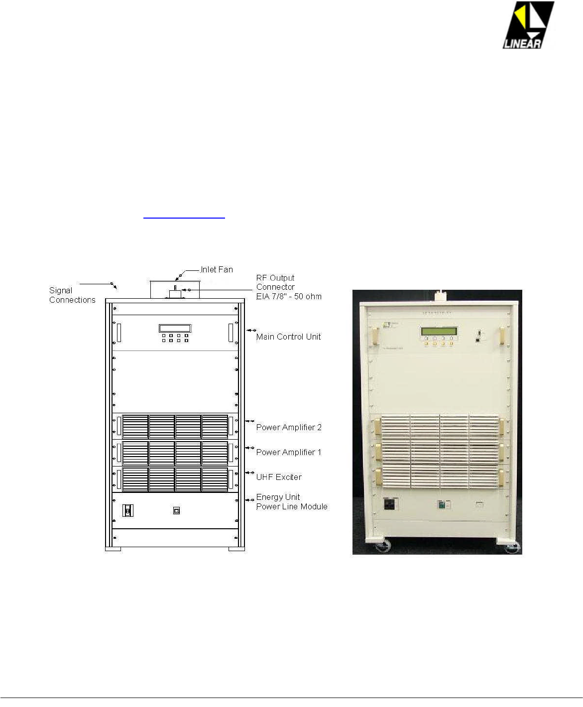
The AT7400 is a 400W UHF ATSC/8VSB transmitter assembled and tested in United States by LINEAR
INDUSTRIES INC. (www.linear-tv.com).
Fig1.1: AT7400 Front View, cabinet wheels are optional.
AT7400 Owner Manual Rev. 2.0 – October 2006-10-23 Section 1 - 2/7 2
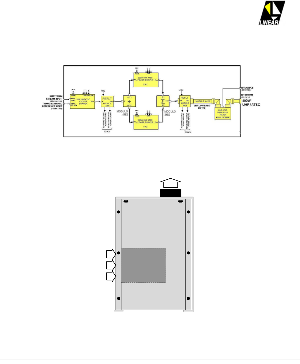
2. AT7400 RF line Up
3. AT7400 Cabinet Air Flux: 0.25m3/sec. - 21ft3/sec.
Fig. 1.4: Air flux path at AT4700 cabinet, (lateral view). Darker area denotes the internal heat source, or the RF drawers,
(1) Exciter and (2) PA’s.
Cold Air Inlet
Air Outlet
AT7400 Owner Manual Rev. 2.0 – October 2006-10-23 Section 1 - 3/7 3
4. AT7400 – 400W UHF ATSC/8VSB Transmitter - Technical Specifications
Electrical
Main 220/240 VAC, bi phase, 50-60 Hz. 3w.
Consumption 3200W.
PFC Included
Signal Input
Transport Stream Input ATSC/MPEG2, compliant to SMPTE310M
Input Data Rate 19.39 Mbps
External Reference Signal 10MHz. (0 to +10 dBm).
Input Connector 75ȍ(BNC),
Reference Input Connector 50ȍ(BNC),
RF
RF Output Power 400w (rms)
Modulation Mode 8VSB. All-Digital Complex IF modulation
IF 18.833916 MHz.
Channel Bandwidth 6MHz.
Test Signal PRBS. Pseudo Random Bit Sequence
Frequency Range UHF. Ch14 to Ch69, (4 bands).
Frequency Step 1 Hz. ± 220kHz
Symbol Rate 10.76 MSymbol/sec.
Digital/Analog Converter 16 bit
All –Digital Linear. Pre-Correction Included
Pilot frequency stability overall ± 0.3 ppm.
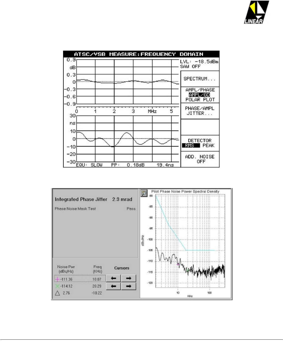
Peak to peak frequency response 0.15 dB.
Peak to peak group delay response 15 ns.
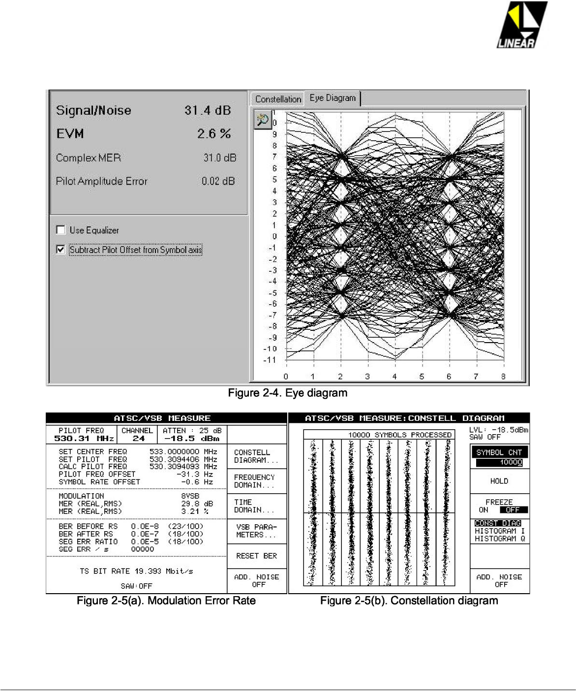
Phase noise -104 dBc/Hz @ 20kHz offset.
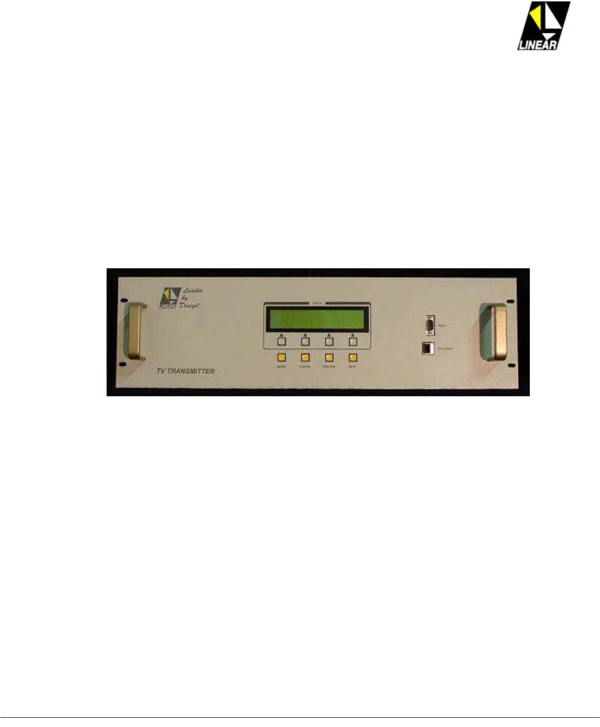
Conducted spurious and harmonics < -60 dBc, FCC 47 Part 74.
Radiated spourious and harmonics < -80 dBc, FCC 47 Part 74.
39dB (modulator output) typical.
39 dB (exciter output) typical.
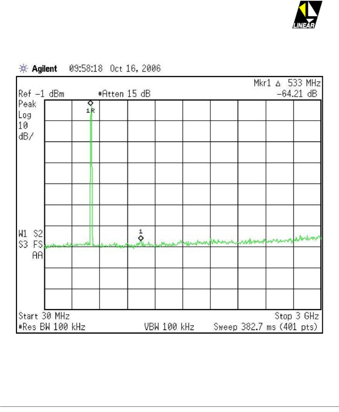
MER (Modulation Error Rate)
29 dB (transmitter output) typical.
RF output connector EIA 7/8” Flanged.
Output sample connector N
Remote Control
RS-232 Dial-up network interface via hyper-terminal
Ethernet SNMP. IP network interface via Web Browser.
Mechanical
Internal drawer’s air speed: 400 ft/minute.
Air Refrigeration Overall Air flow: 21ft3/sec.
Dimensions 58”(H), 28”(W), 43”(D)
Weight Gross: 286.7 Kg NET: 236.70 Kg
Foot print 28”(W), 7’(D)
AT7400 Owner Manual Rev. 2.0 – October 2006-10-23 Section 1 - 4/7 4
5. AT4700 Available Models and Options
Models
AMono-phase; 220Vac.
B3-phase; 220Vac – 380Vac; 3 wires.
C3-phase; 220Vac – 380Vac; 4 wires.
Options:
01 Integrated GPS receiver
02 Adaptive digital pre-correction
03 Dual Exciter
04 Analog Transmission Mode
05 Cabinet 4 wheels
6. AT7400 Typical Test Report
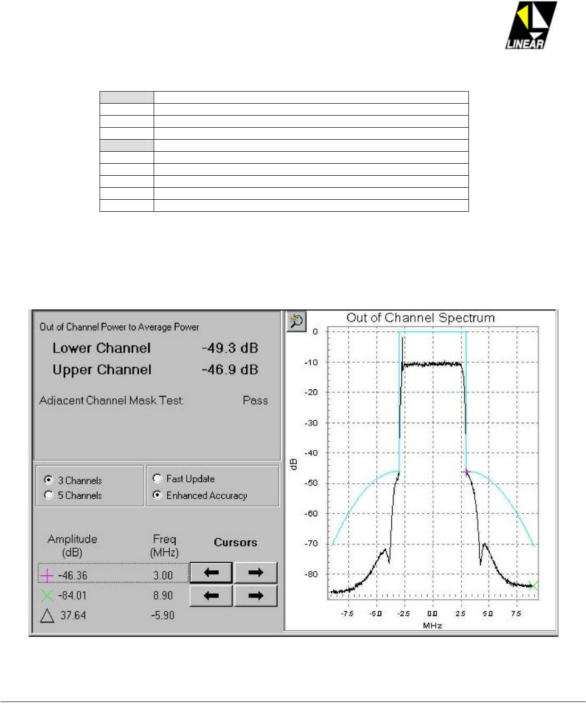
6.1.Out of Channel Emissions
AT7400 Owner Manual Rev. 2.0 – October 2006-10-23 Section 1 - 5/7 5
6.2.Frequency Response and Group Delay
6.3.Carrier Phase Noise
AT7400 Owner Manual Rev. 2.0 – October 2006-10-23 Section 1 - 6/7 6
6.4.Digital Modulation Error Rate
AT7400 Owner Manual Rev. 2.0 – October 2006-10-23 Section 1 - 7/7 7
6.5.Conducted Spurious Emissions
AT7400 Owner Manual Rev. 2.0 – October 2006-10-23 Section 2 - 1/9 1
Section 2 – Master Control Unit
Module 4459
1. General Description
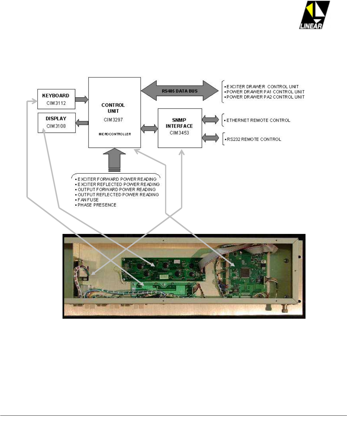
The main control unit, MCU, is the logical master unit acting all over the transmitter operational functions. The
MCU is constantly connected and exchanging information via RS485 with the UHF power amplifiers units and the
UHF exciter unit. External keyboard allows local changing on parameters and monitoring, displayed on a LCD
screen. Via a RS232, it is also possible to implement telemetry using either the Windows Hype Terminal, or via
Ethernet Web Server.
Fig.2.1: – Front View MCU module 4459
2. Following, the main functions of MCU
2.1. Monitor and display the alarm status on each of the transmitter units.
2.2. Monitor the direct and reverse RF power, out from the intermediate directional coupler, module 4488,
avoiding a potential over driver to the power amplifiers.
2.3. Monitor the direct and reverse RF power, out from the output directional coupler, module 4429, and
inhibiting excessive RF power level on either direction.
2.4. Send to the exciter driver local control unit, via RS485 protocol, the set of programmed software instructions
related with the broadcasting channel, and the associated power level.
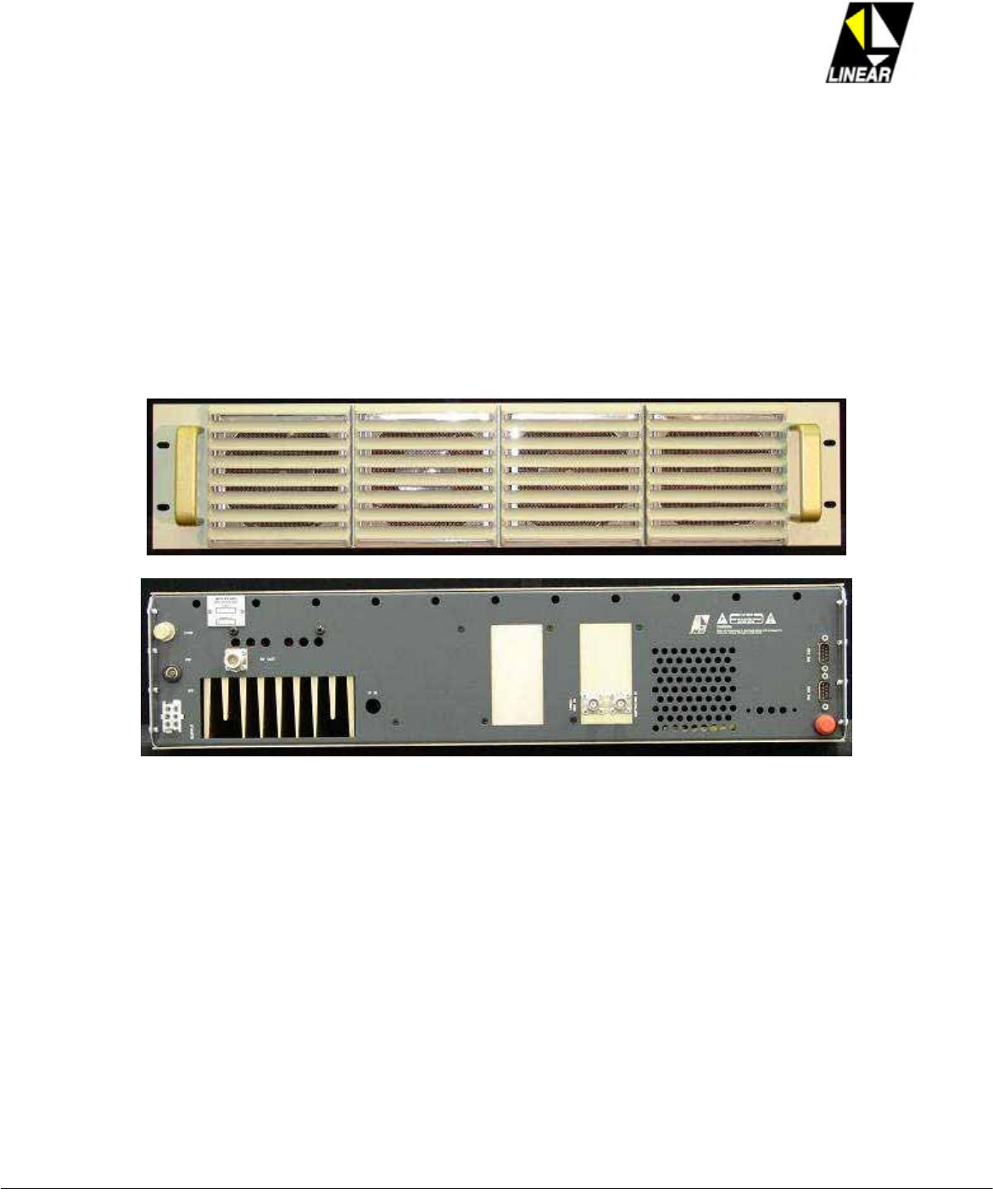
2.5. MCU is composed by the following printed circuit boards:
2.5.1. 01 control unit; CIM3297.
2.5.2. 01 SNMP interface; CIM3453.
2.5.3. 01 Keyboard; CIM3112.
2.5.4. 01 LCD Display; CIM3108.
AT7400 Owner Manual Rev. 2.0 – October 2006-10-23 Section 2 - 2/9 2
2.6.Module 4459 Block Diagram
Fig.2.2: – Module 4459 block diagram and PCBs displacement.
AT7400 Owner Manual Rev. 2.0 – October 2006-10-23 Section 2 - 3/9 3
2.7.Unit Control Board CIM3297 at Module 4459
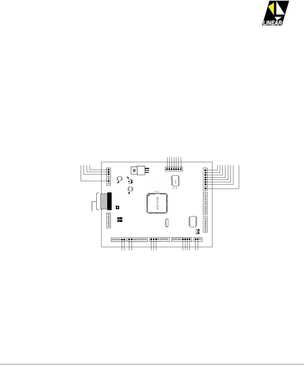
This is the principal board on the MCU module. See Fig.2.5 for the PCB CIM3297 connections. The logic functions
performed by the PCB CIM3297 are as follows:
(YL) BLACK L IGHT DISPLAY ? POI NTA –LC D DISPLAY – CIM3 10 8
(GR) +8V ?PIN7–P1
(WH)GNDTODISPLAY? POINT B – LCD DI S PL AY– CIM 31 08
(BL) +15V ?PIN8–P1
( GY) OUTPUT REF LECT ED POWER READING ?PIN5–P1
( RD) OUT PU TF ORWARD PO WER READING ?PIN6–P1
( VL) 12 V BATTER Y READING ?PIN6–P2
( BR) +8 V DC/DC CO NVERTER READING ?PIN4–P2
( BL) + 15V DC /DC CO NVERT ER READING ?PIN3–P2
( YL) EXCITER F ORWARD PO WER READING ? PIN1–P1
(OR) EXC ITER REFLECTED POWER READING ?PIN2–P1
(WH) GND ?PIN9–P2
(B R) ? PIN4–CON1–KEYBOARD–CIM3112
( RD) ? PI N 3 – CON 1 – KEYBOARD – CIM 31 12
(BL) ? PI N 2 – CON 1 –KEYBOIARD – CIM 3112
( BK) ? PI N 1 – CON 1 – KEYBOARD – CIM 31 12
(O R) ? PIN 6 – C ON 1 – CIM31 12 – KEYB OARD
(GY) ? PIN 5 – C ON 1 – CIM31 12 – KEYBOARD
(Y L) C O AXI AL RELAY COMMANDER ( OPTIO NAL DOUBLE EXC ITER) ?PIN1–P2
(BR) PHASE DETECTOR ?PIN4–P1
( GR) FAN FUSE 1 DETECT OR ?PIN8–P1
( OR) FAN FUSE 2 DETECT OR ? PIN7–P1
FL AT CABLE 14 VIAS ? CON1– LCD DISPLAY –CIM3108
CO N - 1
BL
7
CON-2
1991
3
6CON-7 CON- 8 CO N - 9
1
GND
VCC
DA1
DA2
+15V
IRQ
CON- 3
1
6
CON-4
8
CON-5
8
1
CON-6
8
1
PA 21
PA3 1
PA41
PA51
PA61
PA71
1
PA02
PA12
PA2 2
PA32
PA42
PA52
PA62
PA72
PB01
PB11
PB21
PB31
PB 41
PB51
PB61
PB71
PB 72
PB62
PB 52
PB42
PB3 2
PB22
PB12
PB02
GND
TX
RX
PC6
PC5
GND
A16
A15
A14
A13
A12
A11
A10
A09
GND
A08
A07
A06
A05
A04
A03
A02
A01
CI-7
LM7805
CI -1
123
TPO-1
AJUSTE
LU M . DISPLAY
XTAL1
1
14
SCL
SDA
PM4
PM3
PJ1
PJ0
16MHzDTR
CTS
RX
TX
GND
RTS
DC D
CO N -1 1
1
6
CON-10
1
7
J1 VM
BDM I N
M C 34 06 4
LM358
-
Q1
BCX 5 3
CON-12
1
1
.
DS2 29
..
RS2 32
RS48 5
J4
J5
.
DS22 9
CI -6
CI-2
.
CI-3
.
( BL ) CTR SNMP ? PIN3–CON-1–CI M3 453 – SNM P INTERFACE
(BL) RS485 A ?PIN8–P3 A
B
GND
(GY) RS485B ?PIN7–P3
( BK) DTR SN MP ? PIN7–CON-1–CIM3453–SNMPINTERFACE
( OR) DCD SN MP ? PIN4–CON-1–CIM3453–SNMPINTERFACE
( GR) RTS SNMP ? PIN5–CON-1–CIM3453–SNMPINTERFACE
( YL) CTS SNMP ? PIN6–CON-1–CIM3453–SNMPINTERFACE
( RD) RXD SNMP ? PIN8– CON-1– CIM3453– SNMP INTERFACE
(VL) TXD SN MP ? PI N 9 – CON- 1 – CIM345 3 – SNMP I NTERFACE
(W H) GND SNMP ?PIN2–CON-1 –CIM3453 –SNMPINTERFACE
(YL) BL ACK L IGHT DISPL AY ? POI NTA – LC D DISPLAY – CIM3 10 8
(GR) +8V ?PIN7–P1
(WH)GNDTODISPLAY? POINT B – LCD DI SPL AY– CIM 31 08
(BL) +15V ?PIN8–P1
( GY) OUTPUT REF LECTED POWER READING ?PIN5–P1
( RD) OUT PU TF ORWARD PO WER READING ?PIN6–P1
( VL) 12 V BATTER Y READING ?PIN6–P2
( BR) +8 V DC/DC CO NVERTER READING ?PIN4–P2
( BL) + 15V DC /DC CO NVERT ER READING ?PIN3–P2
( YL) EXCITER F ORWARD PO WER READING ? PIN1–P1
(OR) EXC ITER REFLECTED POWER READING ?PIN2–P1
(WH) GND ?PIN9–P2
(B R) ? PIN4–CON1–KEYBOARD–CIM3112
( RD) ? PI N 3 – CON 1 – KEYBOARD – CIM 31 12
(BL) ? PI N 2 – CON 1 –KEYBOIARD – CIM 3112
( BK) ? PI N 1 – CON 1 – KEYBOARD – CIM 31 12
(O R) ? PIN 6 – C ON 1 – CIM31 12 – KEYB OARD
(GY) ? PIN 5 – C ON 1 – CIM31 12 – KEYBOARD
(Y L) C O AXI AL RELAY COMMANDER ( OPTIO NAL DOUBLE EXC ITER) ?PIN1–P2
(BR) PHASE DETECTOR ?PIN4–P1
( GR) FAN FUSE 1 DETECT OR ?PIN8–P1
( OR) FAN FUSE 2 DETECT OR ? PIN7–P1
FL AT CABLE 14 VIAS ? CON1– LCD DISPLAY –CIM3108
CO N - 1
BL
7
CON-2
1991
3
6CON-7 CON- 8 CO N - 9
1
GND
VCC
DA1
DA2
+15V
IRQ
CON- 3
1
6
CON-4
8
CON-5
8
1
CON-6
8
1
PA 21
PA3 1
PA41
PA51
PA61
PA71
1
PA02
PA12
PA2 2
PA32
PA42
PA52
PA62
PA72
PB01
PB11
PB21
PB31
PB 41
PB51
PB61
PB71
PB 72
PB62
PB 52
PB42
PB3 2
PB22
PB12
PB02
GND
TX
RX
PC6
PC5
GND
A16
A15
A14
A13
A12
A11
A10
A09
GND
A08
A07
A06
A05
A04
A03
A02
A01
CI-7
LM7805
CI -1
123
TPO-1
AJUSTE
LU M . DISPLAY
XTAL1
1
14
SCL
SDA
PM4
PM3
PJ1
PJ0
16MHz16MHzDTR
CTS
RX
TX
GND
RTS
DC D
CO N - 1 1
1
6
CON-10
1
7
J1 VM
BDM I N
M C 34 06 4
LM358
--
MC9S 12A128B
Q1
BCX 5 3
CON-12
1
1
.
DS2 29
.
DS2 29
....
RS2 32
RS48 5
J4
J5
.
DS22 9
.
DS22 9
CI -6
CI-2
.
CI-2
.
CI-3
.
CI-3
.
( BL ) CTR SNMP ? PIN3–CON-1–CI M3 453 – SNM P INTERFACE
(BL) RS485 A ?PIN8–P3 A
B
GND
(GY) RS485B ?PIN7–P3
( BK) DTR SN MP ? PIN7–CON-1–CIM3453–SNMPINTERFACE
( OR) DCD SN MP ? PIN4–CON-1–CIM3453–SNMPINTERFACE
( GR) RTS SNMP ? PIN5–CON-1–CIM3453–SNMPINTERFACE
( YL) CTS SNMP ? PIN6–CON-1–CIM3453–SNMPINTERFACE
( RD) RXD SNMP ? PIN8– CON-1– CIM3453– SNMP INTERFACE
(VL) TXD SN MP ? PI N 9 – CON- 1 – CIM345 3 – SNMP I NTERFACE
(W H) GND SNMP ?PIN2–CON-1 –CIM3453 –SNMPINTERFACE
Fig. 2.3: - Module 4459 connection diagram for PCB CIM3297.
AT7400 Owner Manual Rev. 2.0 – October 2006-10-23 Section 2 - 4/9 4
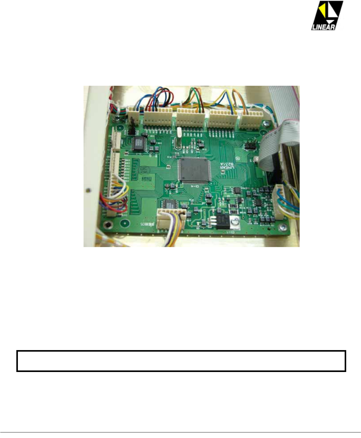
Fig.2.4: – Module 4459, CIM 3297 the transmitter main microcontroller.
2.7.1. Digital Control
oThe integrated circuit CI-4 (A128) is a 16 bit microcontroller, programmed on assembler language. This
integrated circuit controls this module, 4459, and also the entire transmitter. This IC carries a controlled software
version, and is programmed on factory.
oIn case of substitution of the CI-4 or even the entire PCB CIM3297, it is mandatory to inform the factory
prior replacement, the programming identification number that is clearly indicated at the CI-4 body.
AT7400 Owner Manual Rev. 2.0 – October 2006-10-23 Section 2 - 5/9 5
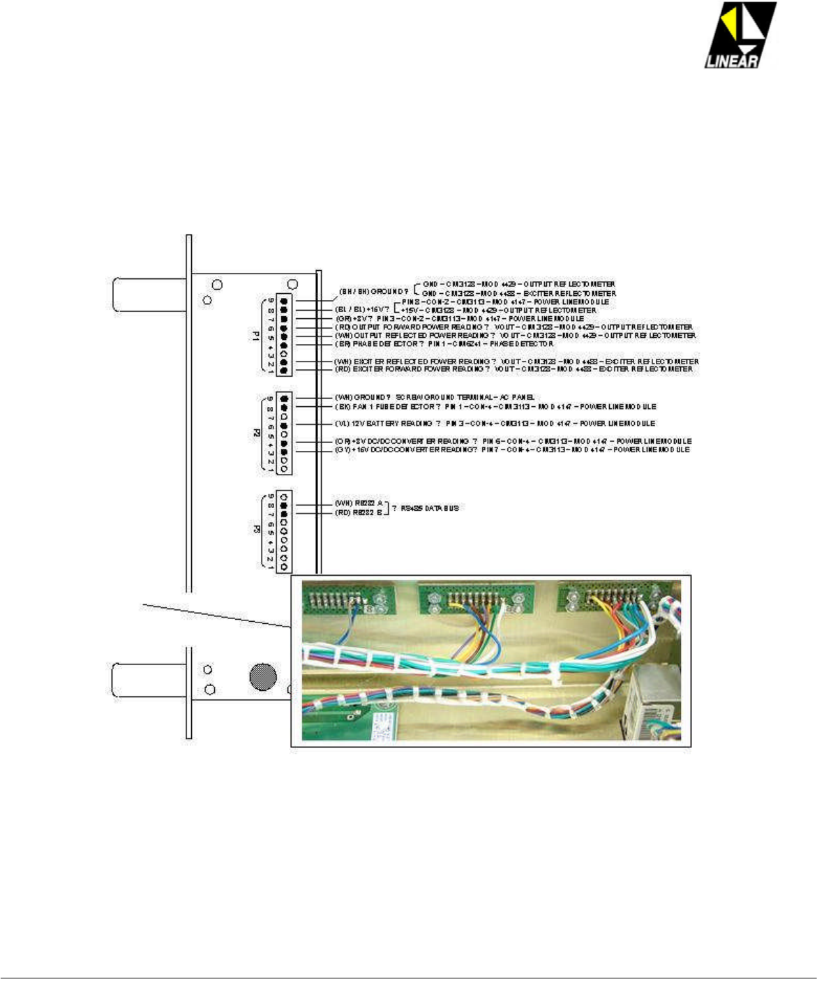
2.7.2. Analog Readings
Information on analog format is available at the connectors P1 and P2 on the module 4459’s panel, which are
routed to CON-9 at the PCB CIM3297. On P1-P2 connectors are available the following analog reading from
external measurements:
Fig. 2.5: - Module 4459 external connections and internal connections view.

AT7400 Owner Manual Rev. 2.0 – October 2006-10-23 Section 2 - 6/9 6
2.7.2.1 Direct RF power, and reverse RF power. From the RF output directional coupler, module 4429.
2.7.2.2 Direct RF driver power, and reverse RF driver power. From the RF intermediate directional coupler,
module 4429.
2.7.2.3 +8V, from the DC/DC converter; module 4147.
2.7.2.4 +15V, from the DC/DC converter; module 4147.
2.7.2.5 The 12V/7Ah battery voltage.
From the connector CON-9 these readings feed the microcontroller CI-4, from where those are digitalized and
processed. By software decision, the microcontroller sets the nominal value for these readings always +4V,
meaning, to all nominal values the +4V will be assigned, and will be available at the CON-9. These values are
transferred to the main LCD display on the MCU.
On the intermediate and final directional couplers, module 4488 and 4429, as well on the mains module, 4147,
there are test points where the +4V nominal reference voltage are set. For instance:
Once on operation and at the time the transmitter is set for its nominal RF output
power, the trim pot TP01 at PCB CIM3128A located at the module 4429 should be
adjust on such way that the +4V is measured at pin 8, on the connector CON-9 located
at PCB CIM3297. More details will be shown on specific sections of this manual.
2.7.3. Alarm Detection
The system alarms are routed to MCU module 4459 via P1 and P2 connectors. These alarms are routed to CON-
5 at PCB CIM3297. These alarms are:
2.7.3.1 Lack of AC phase on mains, detected at module 4147.
2.7.3.2 Open fuse for fan #1, detected at module 4147.
2.7.3.3 Open fuse for fan #2, detected at module 4147. (For 2 racks systems only).
At the time when the system is on normal operation, no alarms, a +5V voltage is sent to the CON-5 via P1-P2
connectors. When an abnormal condition happens, that requires attention and generates an alarm status; a
lower voltage is than sent, usually 0V. When a lower voltage is detected by the microcontroller, the transmission
is halted.
2.7.3.4 The alarm status is shown at the LCD screen on the front panel of the MCU. The alarms events are
classified in two categories regarding the time line occurrence:
2.7.3.4.1. On going alarm situation, noted by the sign “!”.
2.7.3.4.2. Old alarm situation, noted by the sign “#”.
At the time when an alarm source cease, the transmission is reestablished, and the “!” sign is switched to a “#”
sign, and registered. Old records can be manually erased by pressing the key “CLEAR” on the MCU front panel
keyboard.
AT7400 Owner Manual Rev. 2.0 – October 2006-10-23 Section 2 - 7/9 7
2.7.4. RS485 Communication bus
On the PCB CIM3297, pin 1 and pin 2, at the CON-12 perform the RS485 communication link among the MCU,
the UHF exciter driver drawer and the UHF power amplifier drawers.
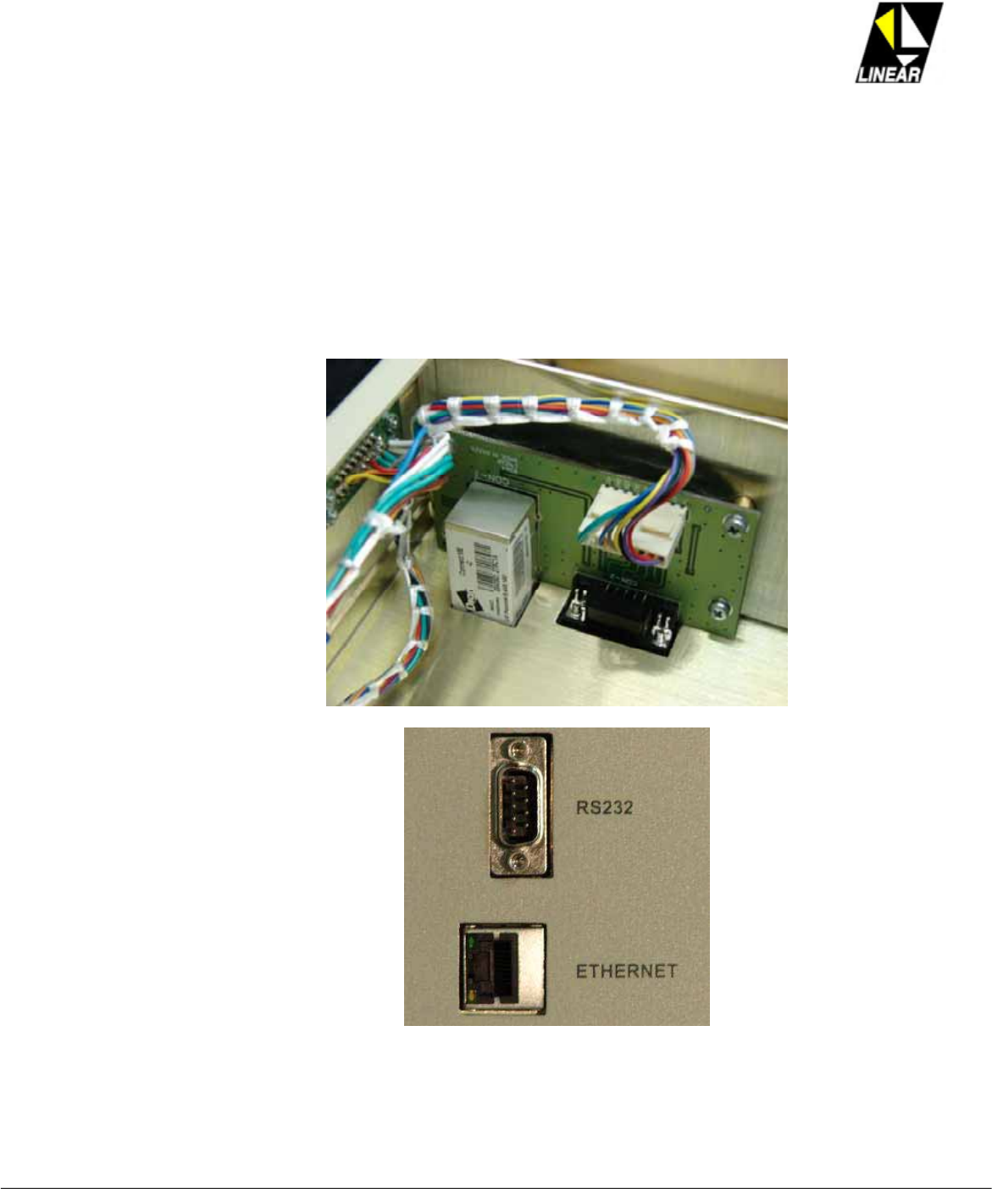
2.7.5. Interface SNMP
The interface SNMP is the PCB CIM3453. The connectors CON-4 and CON-10 located at the PCB CIM 3297
links the 2 PCBs.
Fig. 2.6: - Module 4459 SNPM interface, PCB CIM3453, internal and external view.
AT7400 Owner Manual Rev. 2.0 – October 2006-10-23 Section 2 - 8/9 8
2.7.6. Displaying the Exciter and Power Amplifier Drawers Alarms
Each drawer has its own local control units. The local processed data is link to the MCU via RS485 protocol. The
MCU unit analyze, command actions and display at the LCD, the overall system status.
Alarms from the drawers, are displayed as drawers alarms, followed by one of each signs “!”, or “#”. Any alarm
originated on any internal module belonging to the UHF exciter drawer, that is followed by the sign “!”, (on going
alarm), will cease the transmission. On other hand, any alarm originated on the UHF power amplifier drawer, also
followed by the sign “!”, will cause a proportional RF power reduction, implemented by the MCU logic control.
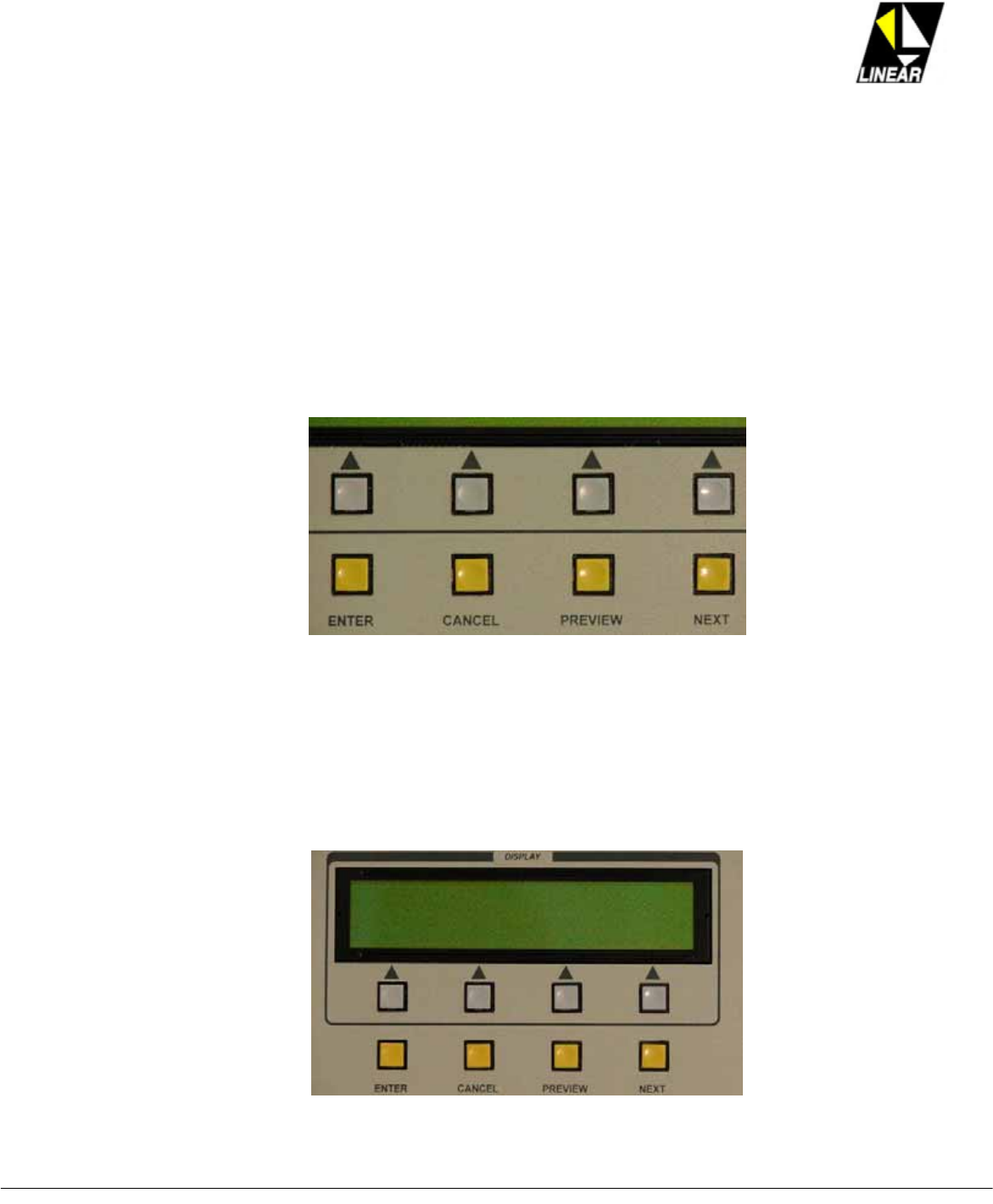
2.7.7. Keyboard, PCB CIM3112
This PCB holds the 8 key pads, which externally allows local manual interface with the transmitter MCU. This
PCB is a switch matrix. CON-1 transfers the CH1-CH8 keyboard ON/OFF operations to the MCU main board.
Fig. 2.7: - Module 4459 local command keyboard, external view.
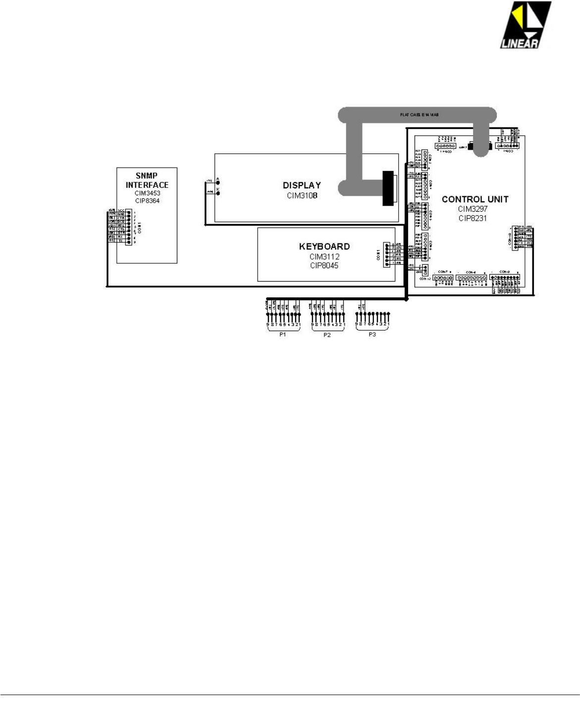
2.7.8. LCD board, PCB CIM3108
This board is 4 rows, 40 columns liquid crystal display, LCD. The board is DC powered by the PCB CIM 3297, a
+5V feed into the point A, (yellow wire) and ground at point K (white wire). A multi-via connector receive a pin-
to-pin data out from CON-2 at PCB CIM 3297, exception for the pin 13 and pin 14 that have each other
exchanged its positions by the flat cable.
Fig. 2.8: - Module 4459 local command keyboard and LCD panel external view.
AT7400 Owner Manual Rev. 2.0 – October 2006-10-23 Section 2 - 9/9 9
2.7.9. Module 4459 Internal Wiring
Fig. 29: - Module 4459 wiring diagram.
2.7.10. Module 4459 Schematic Diagrams: SEE ANNEX A
2.7.10.1 - PCB CIM3297
2.7.10.2 - PCB CIM3112
2.7.10.3 - PCB CIM3108
2.7.10.4 - PCB CIM3453
AT7400 Owner Manual Rev. 2.0 – October 2006-10-23 Section 3 - 1/39
Section 3 – 20W UHF ATSC Exciter
Unit/Drawer GAV4452
1.General Description
The 20W UHF ATSC exciter drawer performs several important functions, as follows:
a. The 8VSB modulation. Incoming SMPTE310 data stream, over an IF carrier, 21.52MHz.
b. Insert the pre-distortion function over the modulated IF signal.
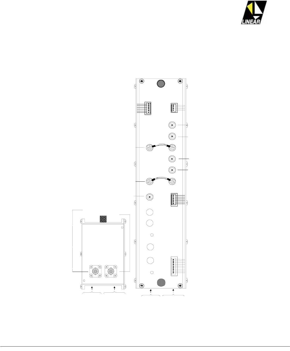
Fig.3.1: Top GAV4452 front view, bottom GAV4452 rear view.
c. Up-convert the IF signal on UHF ATSC broadcast channel.
d. The output RF power control.
e. Generates the 172MHz Master Clock signal, out from a 10MHz stable reference internally originated,
OCXO/0.3ppm oscillator, or externally originated like a GPS source. Automatically switch from INT/EXT
master clock signal source in presence or absence or the EXT signal.
f. Via a DDS circuitry, generates 1Hz steps over the UHF channel frequency.
g. Generates DC voltages for all internal modules, and the +32V externally to the DC/DC converter,
module 4147.
h. The 30W/47dB gain UHF/ATSC power amplifier.
AT7400 Owner Manual Rev. 2.0 – October 2006-10-23 Section 3 - 2/39
The modules assembled into the GAV4452 are:
x01 Module 4454 - 8VSB Modulator and MASTER Clock Generator
x01 Module 4453 - IF/UHF Up-Converter
x01 Module 4466 - DDS
x01 Module 4464 - 20W UHF / ATSC
x01 Module 4456 - Power Supply
x01 Subordinate Control Unit (SCU) – CIM3297
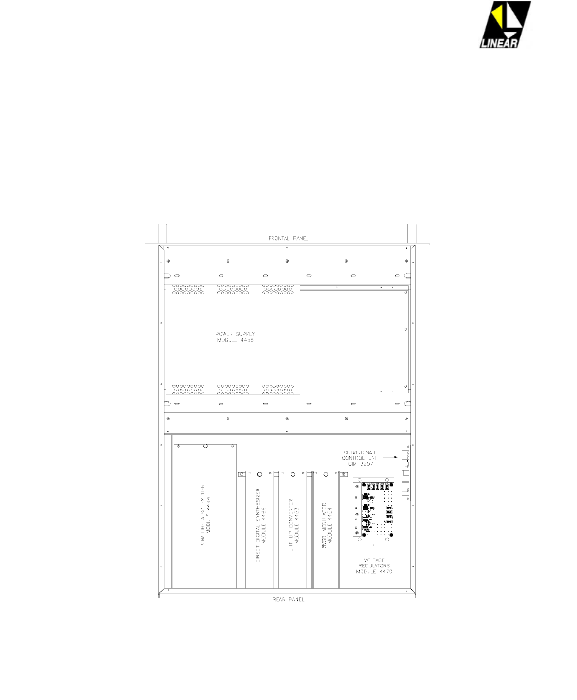
Fig.3.2: GAV4452 modules displacement, top view.
AT7400 Owner Manual Rev. 2.0 – October 2006-10-23 Section 3 - 3/39
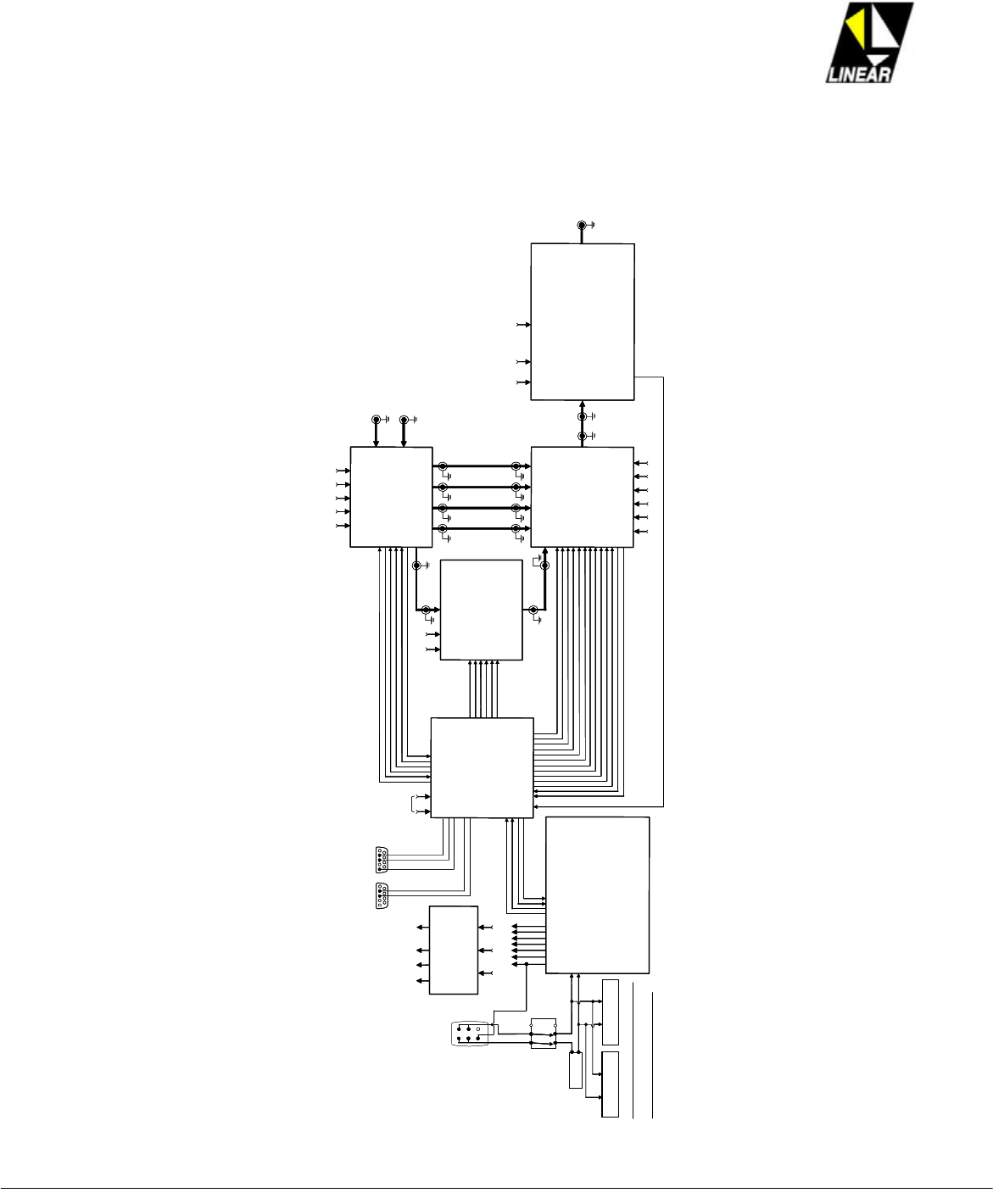
2.GAV4452 – 30W UHF/ATSC Exciter – Block Diagram
+3 2 V
RESTARTED
RFOUT
30W UHF ATSC EXCITER
MO DULE 4455
+12V+5V
SUBORDINATE
CONTROL UNIT
(SCU)
CIM3 297
532
R S 232
32
RS48 5
DAT AI N – DA TAOUT
DATAO UT– DATAIN
MODULATORCLOCK
MODULATORENABLE
MODULATORREAD
LOCK CLO CKALARM
ALC (POWER CONTRO L)
VCO1 C ONT ROL
VCO2 CONTROL
VCO3 C ONT ROL
VCO4 CONTROL
DIV0
DIV1
DIV2
DIV3
DIV4
DIV5
NO IFAL ARM
L OCK DE TEC TOR AL ARM
UHF
UPCO NVERTER
MO DULE 4453
IO RESET
SEND IO
SEND CL OCK
IO UPDAT EC LOCK
MAST ER RESET
SERIALDAT A OUT
DIRECT DIGITAL
SYNTHESIZER
(D DS )
MOD ULE 4 466
8VSB
MODULATOR
AN D M A STE R
CLOCK
MO DULE 4454
II’ QQ’
172MHz
14MHz
+15V
DIRECT
PO WER SU P PL Y
MODU LE 4 456
10AFUSE
+32V REST.
+32V
+32V
+15V DIR.
+15V
SUPPLY
FAN 1
63
52
41
ON/OFF
SWITCH
12
PHA S E 2
O R NE UT RAL
3
PHASE1
4
FA N 2
PHASE 1
PHASE2
ORNEUTRAL
+5V
+2.5V
+ 32 V OUT PUT CURR ENT RE ADI NG
32V O UTPUT VOLTAGE READING
POW ER SUPP L Y RECONNECT I ON
POW ERS UPP L YS HUT DO WN
EXCITER T EMPERATURE ALARM
+15V +5 V
RS232RX
RS2 32 TX
RS2 32 GND
RS485B
RS485A
SM PT E I N
10MHz REFIN
20 8V AC
20 8V MO NOPHAS IC AND 36 0 V TRI PHAS IC EQUI PAME NTS :
•
PHASE 1: 20 8 V
AC
•NE UTRAL
20 8V BI PHAS IC AND 2 08 VT RI PHASI C E QUIPAMENT S:
•
PHASE 1/ PHASE 2:120V
AC
-15V
UHF ATSC
CHANN ELTV
+15V+1.2V -15V+3.3V +5V
+32V+15V+5V -15V+3 . 3V + 12 V
+15V
MO DULE 4470
VO LTAGE
REGULATORS
+5V +2 . 5V
+1 . 2V+3.3V+8V+12V
+3 2 V
RESTARTED
RFOUT
30W UHF ATSC EXCITER
MO DULE 4455
+12V+5V
SUBORDINATE
CONTROL UNIT
(SCU)
CIM3 297
532
R S 232
32
RS48 5
DAT AI N – DA TAOUT
DATAO UT– DATAIN
MODULATORCLOCK
MODULATORENABLE
MODULATORREAD
LOCK CLO CKALARM
ALC (POWER CONTRO L)
VCO1 C ONT ROL
VCO2 CONTROL
VCO3 C ONT ROL
VCO4 CONTROL
DIV0
DIV1
DIV2
DIV3
DIV4
DIV5
NO IFAL ARM
L OCK DE TEC TOR AL ARM
UHF
UPCO NVERTER
MO DULE 4453
IO RESET
SEND IO
SEND CL OCK
IO UPDAT EC LOCK
MAST ER RESET
SERIALDAT A OUT
DIRECT DIGITAL
SYNTHESIZER
(D DS )
MOD ULE 4 466
8VSB
MODULATOR
AN D M A STE R
CLOCK
MO DULE 4454
8VSB
MODULATOR
AN D M A STE R
CLOCK
MO DULE 4454
II’ QQ’
172MHz
14MHz
+15V
DIRECT
PO WER SU P PL Y
MODU LE 4 456
10AFUSE
+32V REST.
+32V
+32V
+15V DIR.
+15V
SUPPLY
FAN 1
63
52
41
ON/OFF
SWITCH
12
PHA S E 2
O R NE UT RAL
3
PHASE1
4
FA N 2
PHASE 1
PHASE2
ORNEUTRAL
+5V
+2.5V
+ 32 V OUT PUT CURR ENT RE ADI NG
32V O UTPUT VOLTAGE READING
POW ER SUPP L Y RECONNECT I ON
POW ERS UPP L YS HUT DO WN
EXCITER T EMPERATURE ALARM
+15V +5 V
RS232RX
RS2 32 TX
RS2 32 GND
RS485B
RS485A
SM PT E I N
10MHz REFIN
20 8V AC
20 8V MO NOPHAS IC AND 36 0 V TRI PHAS IC EQUI PAME NTS :
•
PHASE 1: 20 8 V
AC
•NE UTRAL
20 8V BI PHAS IC AND 2 08 VT RI PHASI C E QUIPAMENT S:
•
PHASE 1/ PHASE 2:120V
AC
-15V
UHF ATSC
CHANN ELTV
+15V+1.2V -15V+3.3V +5V
+32V+15V+5V -15V+3 . 3V + 12 V + 32 V+15V+5V -15V+3 . 3V + 12 V
+15V
MO DULE 4470
VO LTAGE
REGULATORS
+5V +2 . 5V
+1 . 2V+3.3V+8V+12V
AT7400 Owner Manual Rev. 2.0 – October 2006-10-23 Section 3 - 4/39
3.GAV4452 - Module 4454 – 8VSB Modulators and Master Clock
3.1. General Functional Description
The module 4454 can be break down in 2 printed circuit boards. These boards are physically located as the
figure below:
(YL) MODULATOR CLOCK ? PIN3–CON-3–CIM3297–SCU
1
2
3
4
5
6
(BK) DATA IN – DATA OUT ? PIN2–CON-3–CIM3297–SCU
(BL) DATA OUT – DATA IN ? PIN1–CON-6–CIM3297–SCU
(GR) MODULATOR ENABLE ? PIN4–CON-3–CIM3297–SCU
(OR) M ODU LATOR READ ? PIN5–CON-3–CIM3297–SCU
(OR) + 3.3V ? CON-8 – CIM 3458 – MOD.44 70 – VOLTAGE REGULATORS
5
6
7
8
9
(WH) GROUND ? C ON-5 – CIM 345 8 – MOD.44 7 0 – VOL TAGE REGU LATOR S
(OR) + 3.3V ? CON-8 – CIM 3458 – MOD.44 70 – VOLTAGE REGULATORS
(OR) +3.3V ? CON-8 – CIM3458 – MOD.4470 – VOLTAGEREGULATORS
(WH) GROUND ? C ON-5 – CIM 345 8 – MOD.44 7 0 – VOL TAGE REGU LATOR S
(WH) GROUND ? C ON-5 – CIM 345 8 – MOD.44 7 0 – VOL TAGE REGU LATOR S
1
2
3
4
(YL) +1 . 2 V ? CON-9 – CIM3458 – MOD.4470 – VOLTAGEREGULATORS
(YL) +1 . 2 V ? CON-9 – CIM3458 – MOD.4470 – VOLTAGEREGULATORS
(YL) +1 . 2 V ? CON-9 – CIM3458 – MOD.4470 – VOLTAGEREGULATORS
CON-10
CON-11
2
1
6
5
4
3
(BK) -1 5V ? CON-3 – CIM3461 – MOD. 4456 – POWER SUPPL Y
(WH) GROUND ? CON-5–CIM3458–MOD.4470–VOLTAGEREGULATORS
(BR) +5 V ? CON-2–CIM3459–MOD.4456–POWERSUPPLY
(BL) + 15 V ? CON-2–CIM3461–MOD.4456–POWERSUPPLY
(OR) +3.3V ? CON-8–CIM3458–MOD.4470–VOLTAGEREGULATORS
(GY) LOCK CLOCK A LAR M ? PIN4–CON-6–CIM3297–SCU
CON-7
CON-7
CON-6
CON-5
172MH z MASTER CLOCK
CON-5
CON-3
(50O BELDEN CABLE) I +
SIGN AL ? CON-1 – CIM34 42 – M OD.4453 – UHF UPCONVERTER
(50O BELDEN CABLE) I –SI GNA L ? CON-2 – CIM3442 – MOD.44 53 – UH F UPCONVERTER
(50 O BELDEN CA BLE) Q+SIGNAL? CON-4–CIM3442–MOD.4453–UHFUPCONVERTER
(50O BELDEN CABLE) Q–SIGNAL ? CON-5 – CIM3442 – MOD.4453 – UHF UPCONVERTER
(50O BELDEN CABLE) 172MHz MASTER CLOCK ? CON-1 – CIM3456 – MOD.4466 – DDS
172MH z MASTER CLOCK
MA STER CLOCK
CIM3445
8VSB MODULATOR
CIM3444
SMPTE IN
1 0 M H z EXT ER N AL R EFE R ENC E I N
MASTER CLOCK
CIM3445
8VSB MODULATOR
CIM3444
CON-4
CON-3
CON-9
CON-4
(WH) GROUND ? CON-5–CIM3458–MOD.4470–VOLTAGEREGULATORS
1
2
3
4
(WH) GROUND ? C ON-5 – CIM 345 8 – MOD.44 7 0 – VOL TAGE REGU LATOR S
(WH) GROUND ? C ON-5 – CIM 345 8 – MOD.44 7 0 – VOL TAGE REGU LATOR S
(OR) + 3.3V ? CON-8 – CIM 3458 – MOD.44 70 – VOLTAGE REGULATORS
(OR) + 3.3V ? CON-8 – CIM 3458 – MOD.44 70 – VOLTAGE REGULATORS
Fig.3.3: Module 4454 – Left: Front View, Right: Top View.
AT7400 Owner Manual Rev. 2.0 – October 2006-10-23 Section 3 - 5/39
8VSB Modulator
&
pre-distortion
Master Clock
172.16MHz
I
I'
Q
Q'
CIP8357
CIP8358
Sub-module 4454
External
Reference
10MHz
SMPTE 310
Mixer & ALC
PLL + DDS
4xVCO/offset
CIP8355
CIP8356
Sub-module 4453
RF UHF
-2.3dBm
Fig.3.4: Module 4454- 8VSB Modulation and IF/UHF up-conversion structure
3.1.1. Module 4454 - PCB CIM3444: 8VSB Modulator/Pre-Corrector
The PCB CIM3444, is part of the Module 4454. It is the modulator that process the transport stream (TS) that
carries up to 4 broadcast programming including, audio, video and data. All information compressed and
multiplexedinaMPEG2format
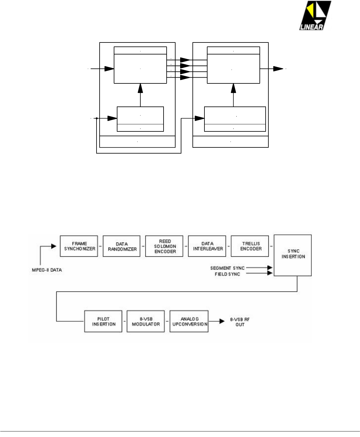
Fig.3.5: CIM3444 – Block Diagram
The 8VSB channel modulator inserts the forward error correction, (FEC), into the transport stream MPEG2. The
modulator follows the ATSC standard A/53 annex D.

AT7400 Owner Manual Rev. 2.0 – October 2006-10-23 Section 3 - 6/39
3.1.1.1 PCB CIM3444 – General Functional Description
The ADVANCE TV series is designed to receive as input signal, programming stream, standard
SMPTE310M,with 19.39M bps, amplitude of 800 mVpp, @75ȍ. The input BNC connector is located on the top
cover of the transmitter rack.
First the circuit to recover the clock rate used to perform the protocol interface. After that there is a rate
equalization of the transport stream, TS, performed by the insertion or delete of the null packets, at the end the
symbol rate is ready to be stabilized and locked with a external/local reference of 10MHz and no longer with the
TS stream that is limited to 2.8ppm accuracy. During this processing is also used the re-stamping for multiple
programs, termed as PCR.
After the data processing as described below, the data stream is ready to receive the channel coding, that is
break down on the following steps:
3.1.1.1.1. Frame Synchronization
For each 188 bytes on the MPEG2 package, this circuit identifies and removes the 47h byte.
3.1.1.1.2. Randomizer
This circuit equally spread the modulated signal energy over the channel band. The final energy density is similar
to a AWGN noise, with this technique, it is possible to achieve a higher bandwidth usage efficiency.
3.1.1.1.3. Reed-Solomom
Reed-Solomon is a block coder, (207,187) that adds 20 redundant bytes on each 187 bytes of the MPEG2
package. With this method it is possible to correct on the reception site, some possible data errors that may had
occurred during the transmission of the RF signal.
3.1.1.1.4. Interleaving
The interleaving technique helps to spread the errors around the time line, making them even less susceptible to
burst errors.
3.1.1.1.5. Trellis Code
Trellis code is closely related to the channel modulation. It is a convolution coder using 2/3 rate, meaning for each
2 bits at the input, there are 3 coded bits at the output creating the 8 symbols used on the 8VSB modulation
process, (-7, -5, -3, -1, +1, +3, +5, +7), having as ultimate goal improve the threshold on the signal-to-noise ratio
of the system.
3.1.1.1.6. Synchronism Insertion
The synchronism insertion built the symbol overall structure, creating the fields and frames as specified on the
A/53E standard.
AT7400 Owner Manual Rev. 2.0 – October 2006-10-23 Section 3 - 7/39
3.1.1.1.7. Pilot Insertion
This part of the circuit adds a small DC level into the carrier to allow a safer and robust reception of the signal.
This DC level is equivalent to 1.25 CU (Constellation Units).
The entire modulation process is digital. This process includes the FIR filters, and do not uses SAW filters to
create the VSB band. Digital modulation increase the quality of the modulated signal measured via a proportional
increase of the MER, (Modulation Error Rate). The modulation process generates 2 identical but orthogonal
signals, termed signals; I and Q. The frequency of the IF carrier is 21.52MHz, and the center of the channel is
18.8MHz.
The value for the system when working with 2 orthogonal carriers is because it is possible to implement
corrections on non-linear distortions, or simply implement digital pre-distortion. The digital pre-correction is
possible using LUT, (Look up Tables). This table synthesizes inverted responses regarding the RF power
amplifier transfer function, reducing the IMD products.
The digital processing generates I and Q distorted, and these 2 signals are than converted to the analog format
via a 16 bits DAC, with 2 balanced outputs, on a total of 4 output analog signals. These signals are termed; I, I’, Q
and Q’, and are respectively present at the CN9, CN8, CN6, and CN5 connectors at CIM3444. These 4 signals
will become the UHF Up-Converter input signals, Module 4453.
3.1.2. Module 4454 - PCB CIM3445: Master Clock
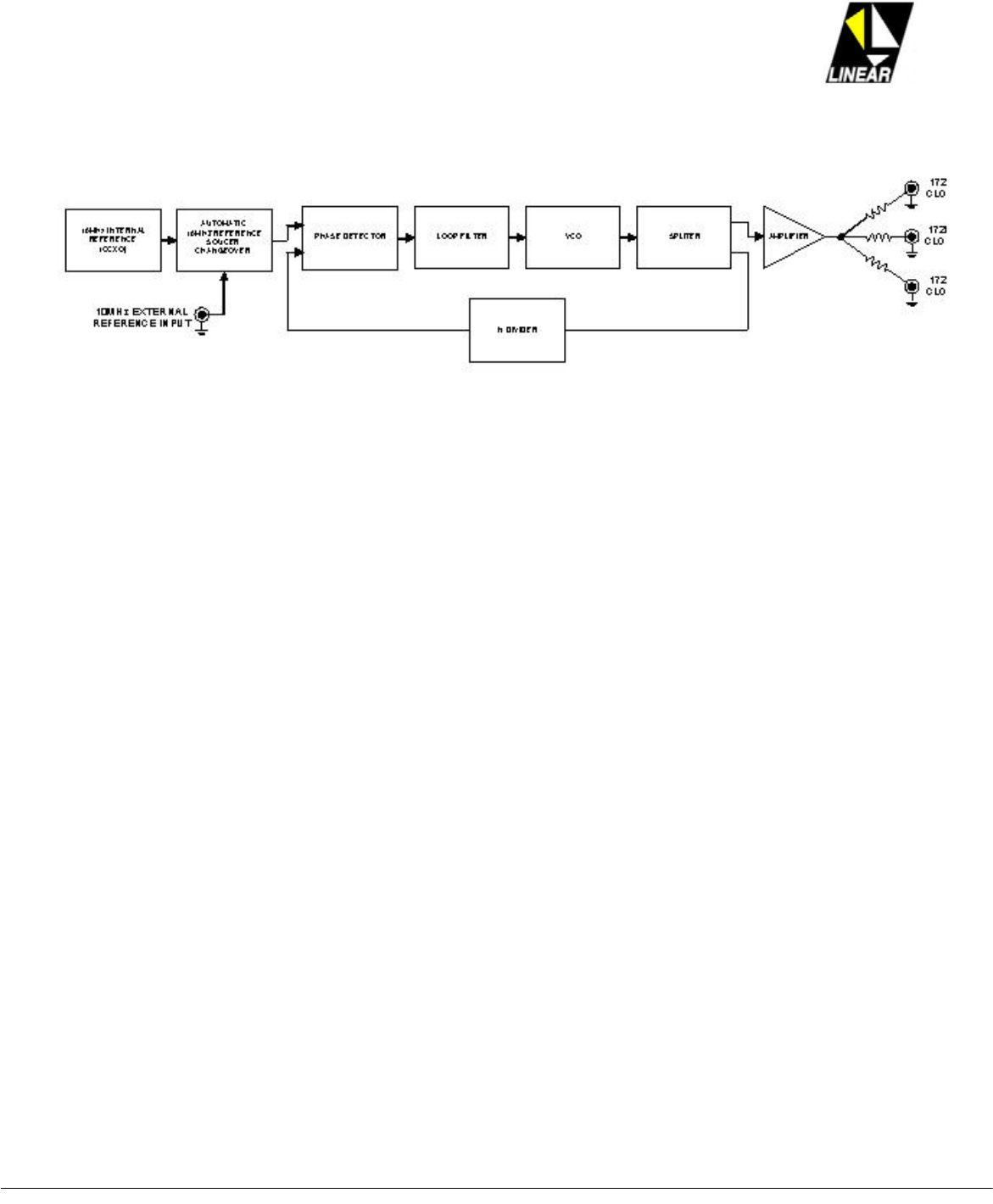
Fig.3.6: External Reference input BNC connector
The Master Clock PCB CIM3445, embedded into the module 4454, out
from a 10MHz internal/external reference signal, synthesizes a
172.16MHz oscillator that represents 16 times the symbol rate of the
modulator 8VSB
This oscillator signal is squared by a schimitt trigger circuit with amplitude
equal to 0-3.3 volts. This square wave type signal is the master clock
signal that will synchronizes all the digital circuits on this equipment
except the control signals.
AT7400 Owner Manual Rev. 2.0 – October 2006-10-23 Section 3 - 8/39
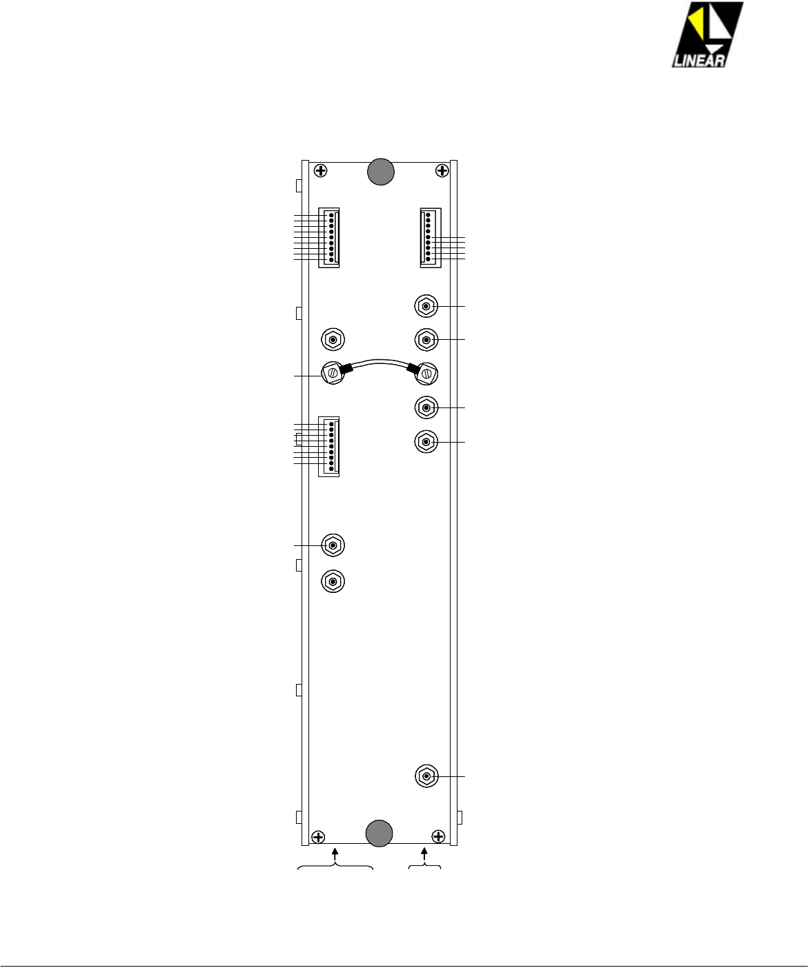
3.1.3. PCB CIM3445 – Master Clock - Block Diagram
3.1.4. PCB CIM3445 – General Functional Description
The 172.16MHz frequency is synthesized via a PLL, a VCO and a DDS circuit. The 10MHz reference is one out of
the two inputs of the phase comparator. This signal comes to CIP8358 via a SMB connector, CON-2. The second
one is also a 10MHz generated by the DDS circuit out from the free running 172.16MHz oscillator.
The loop filter performs the integration of the phase comparator output, generating the error signal that is feed
back to the VCO. On this way the VCO is locked to the reference signal.
The oscillator signal is delivery via 3 connectors. Two of those are routed to the 8VSB Modulator, PCB CIM3444,
and the third one is routed to the DDS circuit, module 4456.
3.2. Module 4453 - UHF ATSC Up-Converter
The Up-Converter module is composed by the mixer circuitry, PCB CIM3442, and a local oscillator, PCB
CIM3443.
AT7400 Owner Manual Rev. 2.0 – October 2006-10-23 Section 3 - 9/39
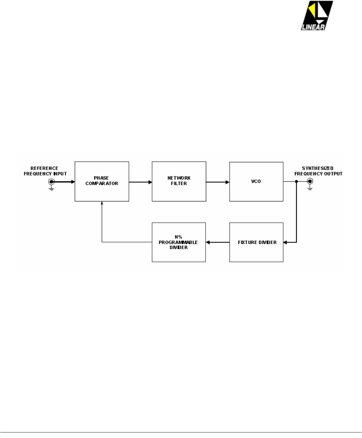
3.2.1. Module 4453 - External Connections
LOCAL OSCILATOR
CIM3443
MIXER
CIM 3442
(BK) NO IF ALARM ? PIN5- CON-6–CIM3297 –SCU
5
6
7
8
9
(GY) +12V? CON-6–CIM3458–MOD.4470–VOLTAGEREGULATORS
(BR) +5V? CON-2–CIM3459–MOD.4456–POWERSUPPLY
(WH / RD) ALC (POWER CONTROL) ? PIN 4 – CON-1 – CIM329 7 – SCU
(SH) GROUND ? PIN2 –CON-1–CIM3297 –SCU
1
2
3
4
CON-7
CON-1
CON-2
CON-3
CON-4
CON-5
CON- 6
LO OUTPUT
CON-6
CON-3
(50ȍBELDEN CABLE ) I+SIGN AL ? CON-9–CIM3444–MOD.4454 –8VSBMODULATOR
(50ȍBELDEN CABLE) I–SIG NAL ? CON-8 – CIM3444 – MOD.4454 – 8VSB MODULATOR
(50ȍBELDEN CABLE ) Q+SIG NAL ? CON- 6 – CIM3444 – MOD.4454 – 8VSB MODULATOR
(50ȍBELDEN CABLE) Q–SIG NAL ? CON- 6 – CIM3444 – MOD.4454 – 8VSB MODUL ATOR
(50ȍBE LDEN CABLE ) 14M Hz REFERENCE ? CON-2–CIM3456–MOD.4466 –DDS
2
1
6
5
4
3
(BK) -15V ? CON-3–CIM3461–MOD.4456–POWERSUPPLY
(WH) GROUND ? CON- 5 – CIM3458 – MOD.4470 – VOLTAGE REGUL ATORS
(OR) +3.3 V ?CON-8–CIM3458–MOD.4470–VOLTAGEREGULATORS
(BL) +15V ? CON-2–CIM3461–MOD.4456–POWERSUPPLY
(VM) +32 V ? CON- 10– CIM3447 – MOD.4456 – POWER SUPPLY
(OR) VCO4 CONTROL ? PIN8 –CON-4–CIM3297 –SCU
CON-2
7
8
9
(VL) VCO3 CONTROL ? PIN6 –CON-4–CIM3297–SCU
(GY) VCO2 CONTROL ? PIN2 –CON-4–CIM3297 –SCU
(BR) VCO1 CONTROL ? PIN6 –CON-3–CIM3297–SCU
2
1
6
5
4
3
(BR) DIV1 ? PIN5–CON-5–CIM3297–SCU
(WH) GROUND ? CON- 5 – CIM3458 – MOD.4470 – VOLTAGE REGUL ATORS
(CZ) DIV0 ? PIN 6 – CON-5 – CIM3297 – SCU
(OR) DIV2 ? PIN 4 – CO N-5 – CIM3297 – SCU
(BK) DIV3 ? PIN 3 – CON-5 – CIM3297 – SCU
(VL) DIV4 ? PIN2–CON-5–CIM3297–SCU
CON-1
7
8
9
(VM ) DIV5 ? PIN1–CON-5–CIM3297–SCU
(GR) LOCK DETEC TOR ALARM ? PIN3 –CON-6–CIM3297 –SCU
(50ȍBELDEN C ABLE) UHF / ATSC CHANNEL TV ? CON -1 – CIM3446 – MOD.4455 – 30W UHF EXCITER
CON-4
CON-5
AT7400 Owner Manual Rev. 2.0 – October 2006-10-23 Section 3 - 10/39
3.2.2. PCB CIM3443 – Local Oscillator
The local oscillator is designed based on a PLL circuit. This oscillator is able to synthesize frequencies within the
band from 450MHz up to 900MHz. To guarantee a high quality signal generation out from the local oscillator, 4
VCO’s (voltage controlled oscillator) were implemented with a shift frequency range of 125MHz each. Just one
VCO works at the time to avoid interferences. On this arrangement, a 102dBc@20Hz phase noise is achieved.
The synthesizer on the feedback loop select the desired frequency inside the choose VCO band.
The VCO’s signal outputs are isolated among them via a sum and inverted circuits. The reference frequency
generated by a DDS circuitry complete the Up-conversion frequency process. The output local oscillator signal
power is +5dBm.
3.2.3. PCB CIM3443 – Local Oscillator – Block Diagram
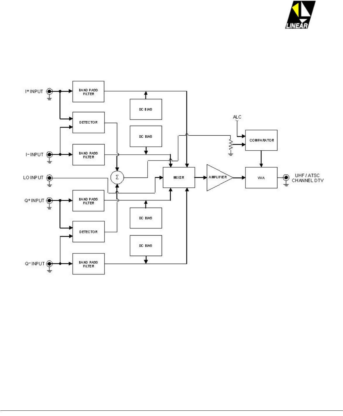
3.3. PCB CIM3442 – UHF Mixer
The mixing operation translates the IF modulated signal frequency up to the assigned UHF broadcasting channel,
the operation utilizes the complex approach considering the orthogonal pair of signals (I-, I+) and (Q-,Q+) allowing
rejection of one side band, and the oscillator itself. The rejection is around 40dB, facilitating the post filtering
steps.
Right after the mixing operation, the now RF signal is 10dB broadband (VHF and UHF) amplified under a typical
2dB roll-off characteristic. The RF output pass through a 25dB dynamic range variable attenuator. The control of
this attenuator is related with the DC level generated by the ALC (Automatic Level Control). In case of absence of
a IF signal or valid IF signal (locked via PLL) of any of the 4 possible IF signals, the attenuator assumes it higher
level of attenuation, and shutting down the RF chain of amplification.
AT7400 Owner Manual Rev. 2.0 – October 2006-10-23 Section 3 - 11/39
3.3.1. PCB CIM3442 – UHF Mixer – Block Diagram
AT7400 Owner Manual Rev. 2.0 – October 2006-10-23 Section 3 - 12/39
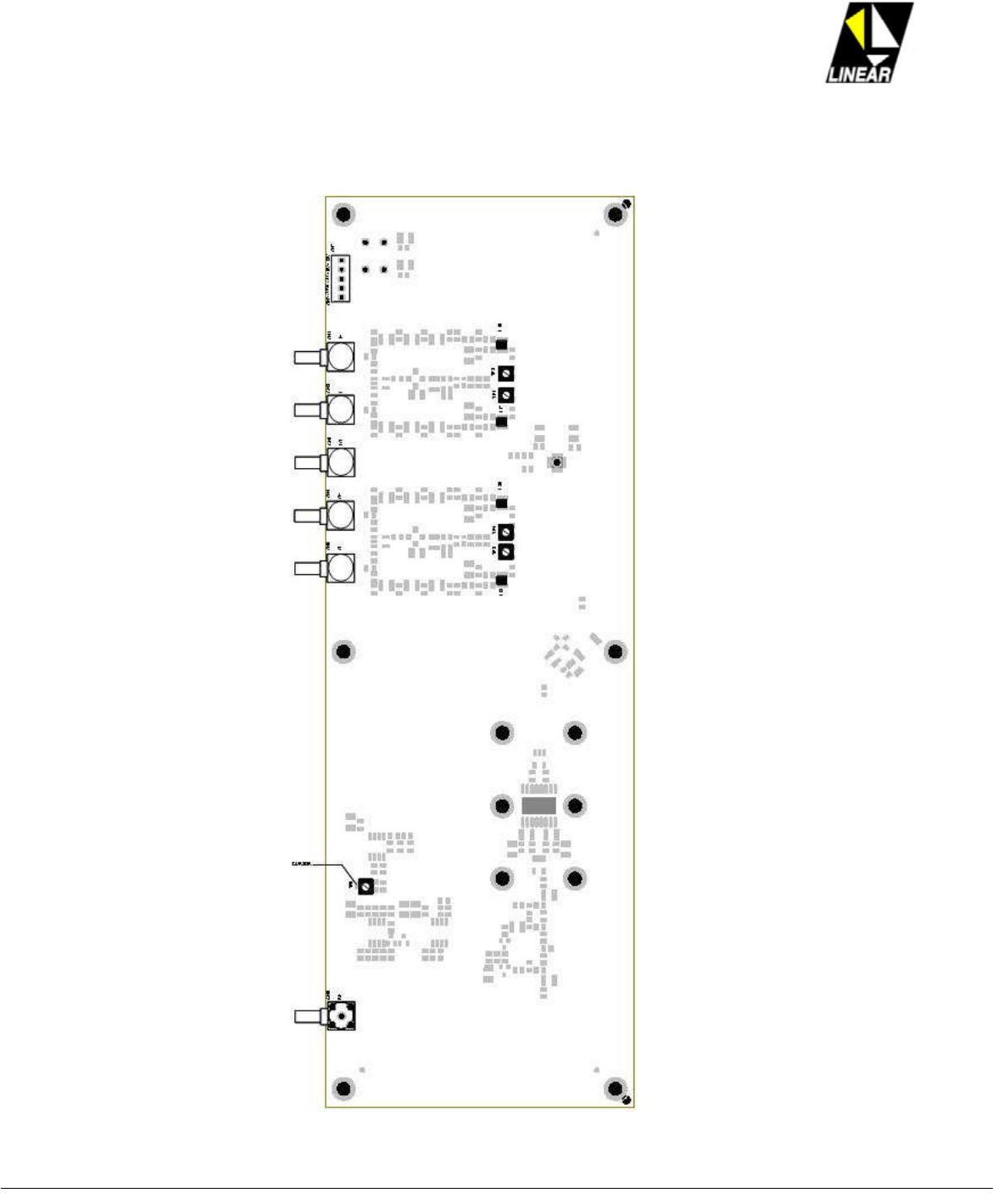
3.3.2. PCB CIM3442 – UHF Mixer – Test Points Diagram

AT7400 Owner Manual Rev. 2.0 – October 2006-10-23 Section 3 - 13/39
3.3.3. PCB CIM3442 – UHF Mixer – Adjustment Procedures
The mixer-ALC circuitries have 2 types of adjustments. The first one is a DC level that polarizes each branch of
the input of the complex mixer. Each one of the DC levels must be adjusted seeking for the max rejection on the
un-desired vestigial side band, in conjunction with the LO rejection as well. The level adjustments are performed
by the trim pots: TPO-1, TPO-2, TPO-3, and TPO-4. Voltage range of +1.4V to +1.6V should be present on the
following test points.
xTPO-1: readings on L17
xTPO-2: readings on L18
xTPO-3: readings on L19
xTPO-4: readings on L20
The second set of adjustments follows the first one. Once the first set is completed, the fine tuning adjustment
should be performed. It is necessary to connect the spectrum analyzer to the UHF RF output of the sub-module
4453. At this point, either the LO signal, as the superior RF spectral image of the UHF/ATSC RF channel, must be
attenuated by 40dBc.
40dBc
UHF / ATSC
CHANNEL DTV
(BELOW MIXING)
LOCAL OSCILATOR
SIG NAL
UHF / ATSC
CHANNEL DTV
(ABOVE MIXING)
40dBc
UHF / ATSC
CHANNEL DTV
(BELOW MIXING)
LOCAL OSCILATOR
SIG NAL
UHF / ATSC
CHANNEL DTV
(ABOVE MIXING)
Fig.3.7: Level references for mixer-ALC fine tuning
The second adjust detects the protection signal at the center of the band. In absence of 1 out of 4 controls IF
signals, this DC level exceed the min threshold and shut down the RF output signal. The DC threshold adjust is
performed by TPO-5, and should be set for +2.5V.
3.4. Module 4466 – Direct Digital Synthesizer (DDS)
The module 4466 is a signal reference generator based on a DDS circuit. This module is able to synthesize
frequencies up to 50MHz under mHertz precision range. The signal is used as PLL reference on the UHF Up-
Converter module 4453 – PCB CIM3442. The RF channel 10kHz off-set if necessary, is pre-set on the DDS
circuitry. The phase noise on the reference signal generated on this module is better than 110dBc/Hz.
The SCU unit – PCB CIM3297 – configures the DDS’s circuitry parameters via a serial communication port. The
DDS module receives a signal out from the master clock module 4454 - PCB CIM3445; perform the programming
operation for the RF output channel as required under mHertz precision. At the end, is expected a frequency error
around 1Hz max., when measured at the output of the UHF mixer circuit. Before leaves the module, the DDS
signal is amplified and filtered.
AT7400 Owner Manual Rev. 2.0 – October 2006-10-23 Section 3 - 14/39
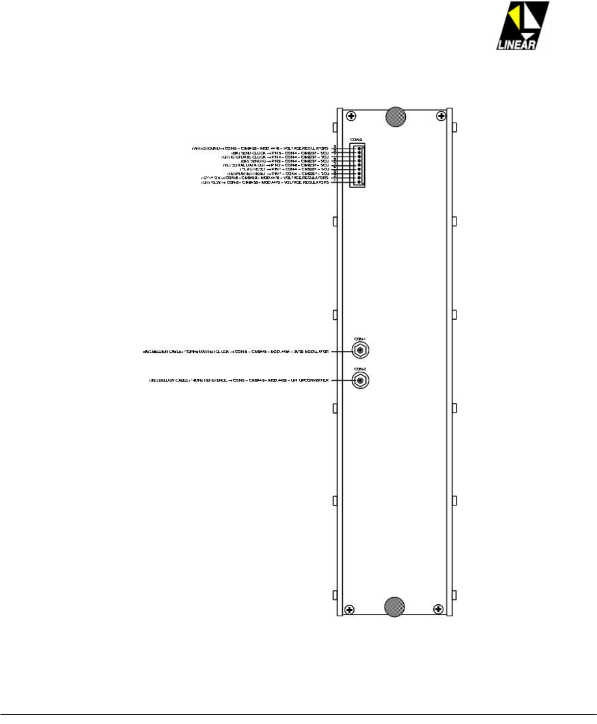
3.5. Module 4466 – External Connections
AT7400 Owner Manual Rev. 2.0 – October 2006-10-23 Section 3 - 15/39
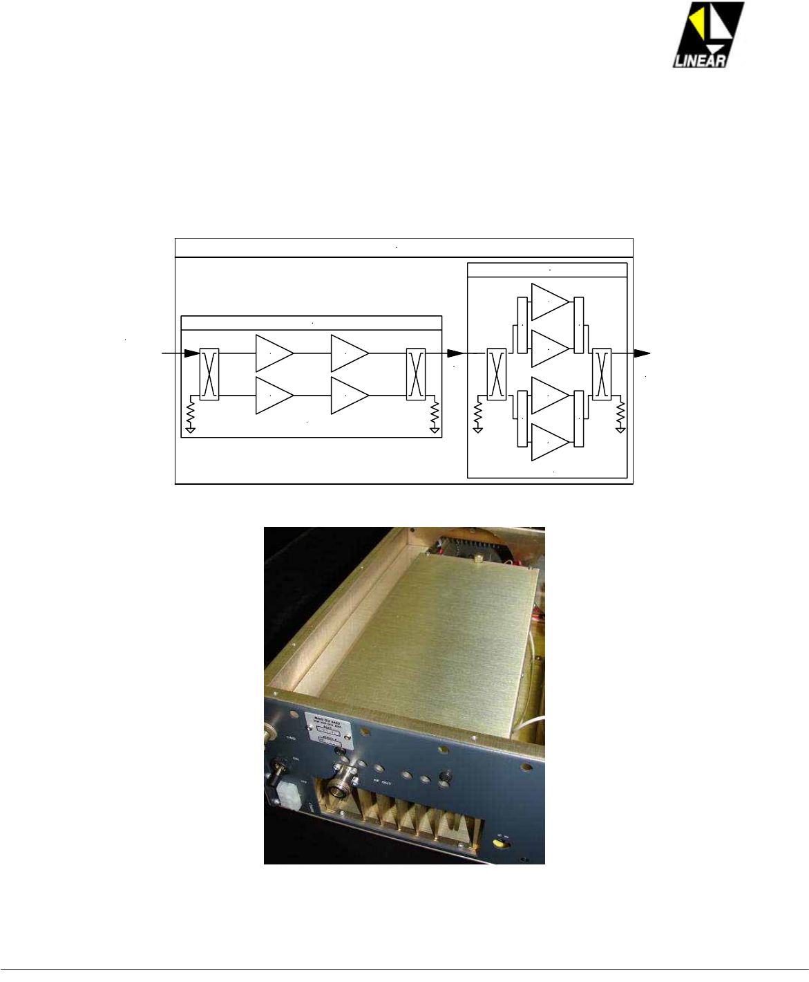
3.6. Module 4464 – 20W UHF ATSC Power Amplifier
The RF/UHF signal, already set to the assigned channel, is than power amplified up to 20W. The RF amplifier is
type class AB. LDMOS transistors are also used on this amplification stage. Fig.:3.2; illustrates the RF chain of
the module 4464.
RF UHF
-2.3dBm
Printed Circuit Board CIM 3446
SG9289 BLF1822
BLF1822SG9289
G = 16dB
G = 32dB
Printed Circuit Board CIM 3440
H
H H
H
RF UHF
20W
RF UHF
0.5W
Module 4455: 20W power amplifier
BLF861A
BLF861A
BLF861A
BLF861A
Fig.3.8: UHF 48dB gain RF amplification chain, simplified block diagram
Fig.3.9: Module 20W UHF ATSC power amplifier – module 4464
AT7400 Owner Manual Rev. 2.0 – October 2006-10-23 Section 3 - 16/39
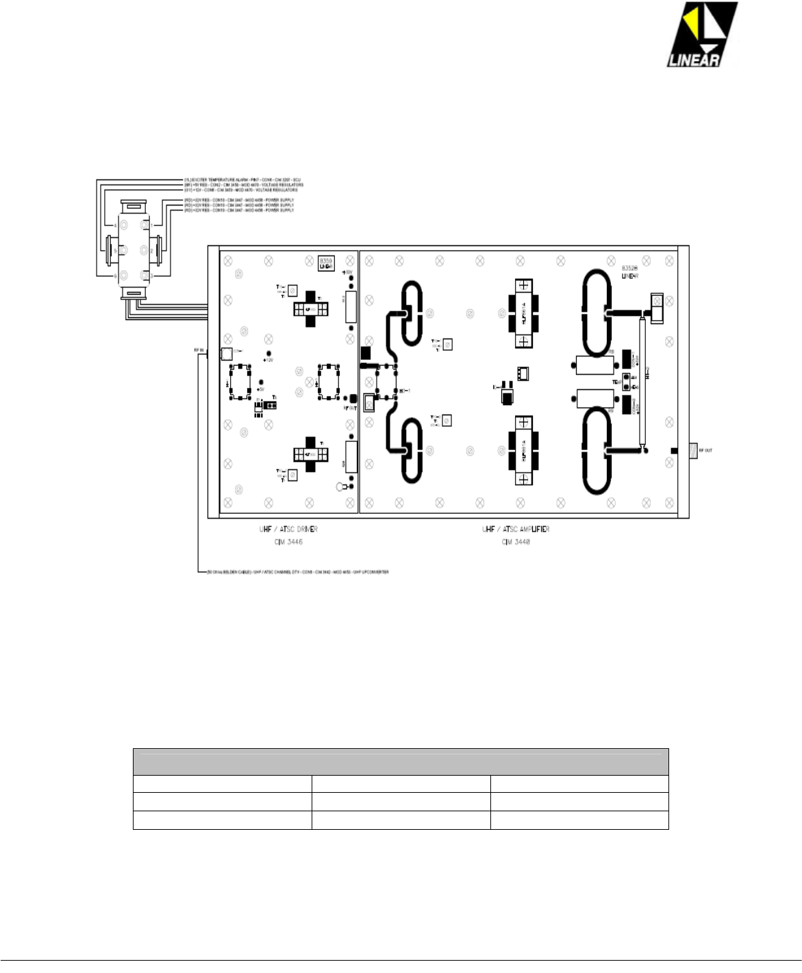
3.1.3.1 General Functional Description
The PCB CIM 3390 delivers is the output nominal ATSC UHF 20W output power for the module 4455 –
intermediate directional coupler. Despite the amplifier being designed as a broadband amplifier, due optimization
reasons, the amplifier is built in 4 frequency operational bands, as follows:
xchannel 14 to 25 (B1) - channel 26 to 38 (B2) - channel 39 to 53 (B3) - channel 54 to 69 (B4)
Despite the different bands, the PCB remains the same, as indicated on the table below:
20W UHF / ATSC EXCITER - MODULE 4464
CIRCUIT CIM CIP
DRIVER 3446 8359
FINAL STAGE 3440 8352
Table 3.1: Module- 4464 PCB assembles references.
NOTE: CIM stands for the PCB version, and CIP stands for the bill of material version.
AT7400 Owner Manual Rev. 2.0 – October 2006-10-23 Section 3 - 17/39
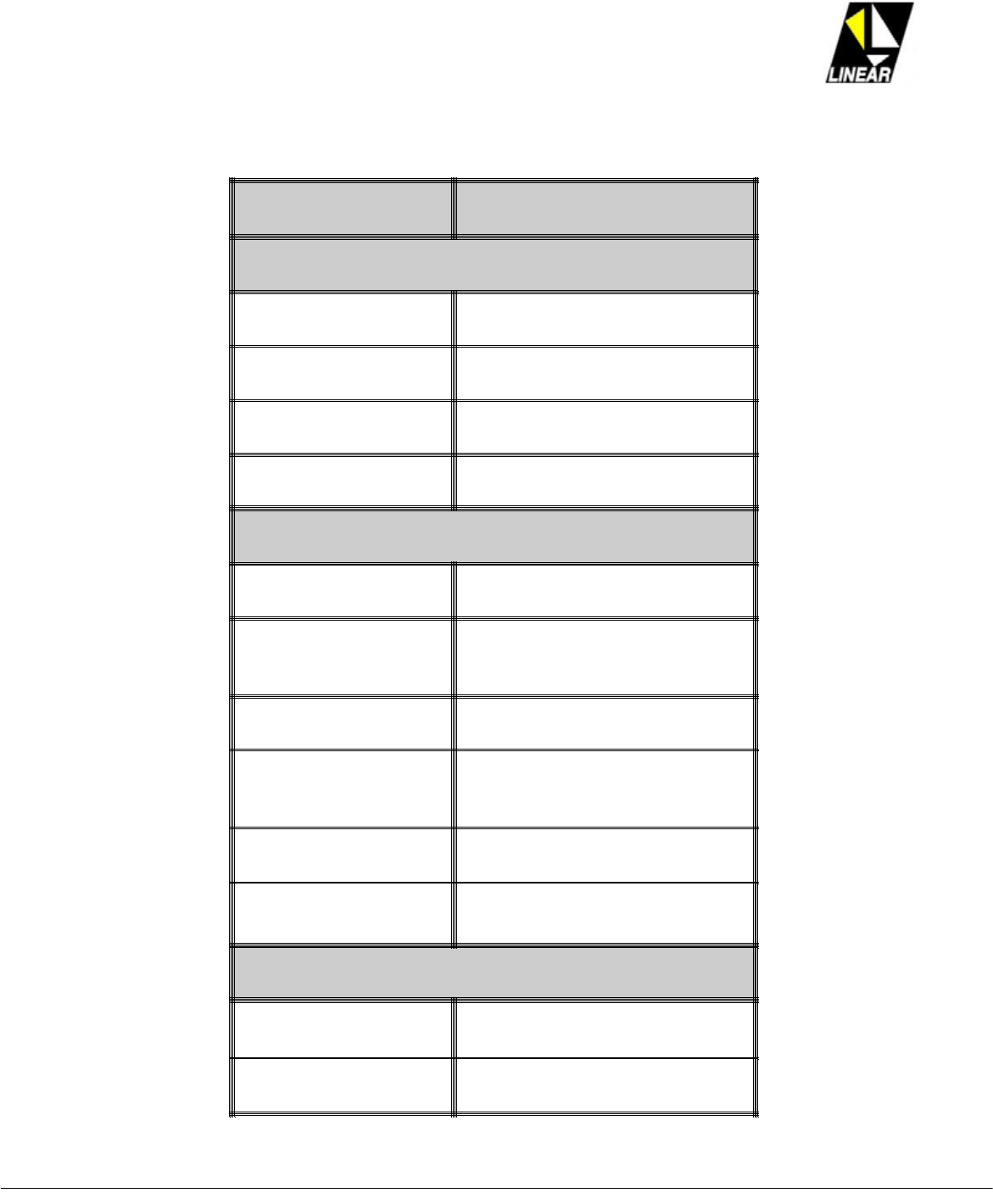
3.9.1. Module 4464 – Technical Specifications
CHARACTERISTIC SPECIFICATION
SMPTE310M INPUT
FREQUENCY 470 - 862MHz
IM P E D A NC E 7 5 Ohm s
CONNECTOR BNC FEMALE
RETURN LOSS ³22dB
RF OUTPUT
GAIN FROM 45 TO 48dB
ATSC
AVERAGE POWER UNTIL 20W
HARMONICS £ -60dB
SPURIOUS
EMISSION < -54dB
INTERMODULATION < -52dB
CONECTOR N FEMALE
GENERAL
POWER SUPPLY +32V / +12V / +5V
CONSUMPTION 14A (AB CLASS)
AT7400 Owner Manual Rev. 2.0 – October 2006-10-23 Section 3 - 18/39
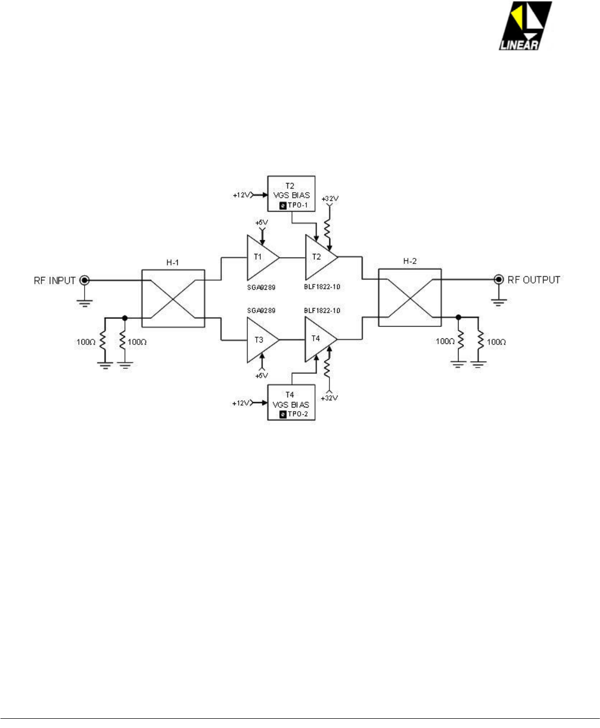
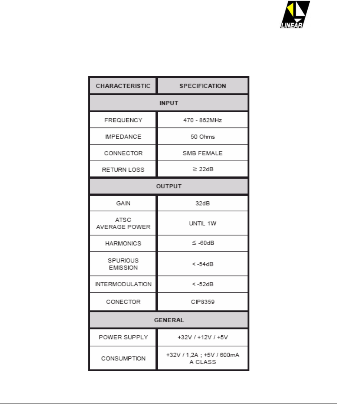
3.9.2. Module 4464 – PCB CIM3446 – 32dB Gain Driver 0.5w Amplifier
The PCB CIM 3446 is the driver amplifier for the 20W final amplifier. This circuit is 2 parallels cells, type class A
polarization, 90 degree out of phase, able to delivery up to 1W of power usable for DTV/ATSC standard over the
470MHz – 806MHz UHF band.
Fig.3.9: Module 4464 – CIM3446 – block diagram
Each amplification cell is composed first by a BJT transistor followed by a LDMOS transistor. The serial
connection of these 2 devices delivery 500mW.The parallel combination of these 2 cells via H-2 hybrid, is able
than to delivery 1W of RF power.
AT7400 Owner Manual Rev. 2.0 – October 2006-10-23 Section 3 - 19/39
3.9.3. Module 4464 – CIM 3446 – Technical Specifications
AT7400 Owner Manual Rev. 2.0 – October 2006-10-23 Section 3 - 20/39
3.9.4. Module 4464 – PCB 3446 – Adjustment Procedures
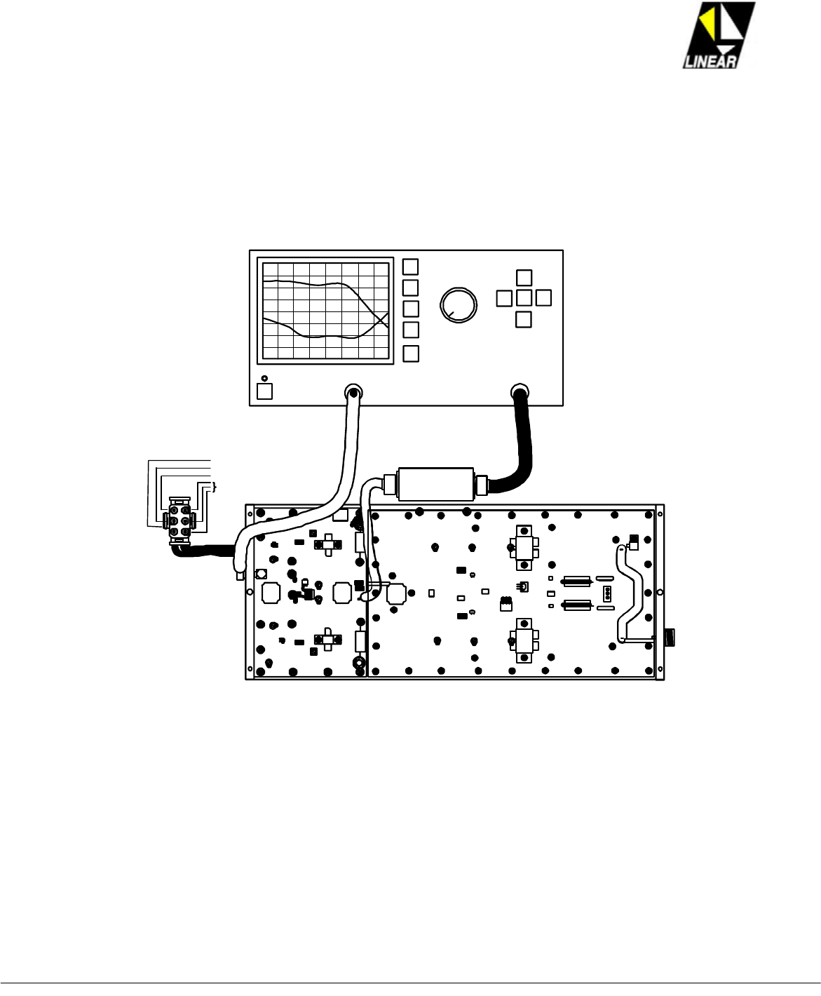
The PCB CIM3446 can be adjusted either locally, meaning inside of the equipment, (recommended for simplicity)
or outside of the equipment. On either situation, one MUST always use a 50ȍload connected at the RF output.
RF IN
+32V / 2A VOLTAGE
SUPPLY
3
2
1
6
5
4
RF IN
RFOUT
NETW ORK ANALYZER
+12V / 1A VOLTAGE
SUPPLY
+5V / 1A VOLTAGE
SUPPLY
+32V
T2
T4
R1 3R28
TP O-2
VGST4
HI -2
HI-1
CON -1
T3
T1
C41
C4
TPO -1
VGS T2
C13
+12V
+5V
R7
R23
R14
R15
.
BLF1822
BLF1 822
(GY )
(BR)
(RD)
(RD)
83 5 9
LI N E A R
MODULE 4464
30dB / 50W
ATTENUATO
R
6
5
.
.
C5
C9
C13
T1
C3 5
C3 9
T2
CI-4
CI-2
TP O-2
T2
VGS ADJ
TPO-1
VGSADJ
T1
CI -1
HC-1
R9
R10 +32V
CON-2
CON-2
+32V
CON- 3
ID1
ID2
TE MP
R11
BLF861A
.
CI -3
S1
.
CI -5
.
CI-7
.
CI-8
T4
T3
BLF 861A
+32V / 2A
EXCITER TEMPERATURE
ALARM
3.9.4.1 Drain Current, (ID) - Adjust for T2 and T4
No RF signal should be present at the RF input of the module 4464. Turn the module ON and wait for 3 minutes
for thermal stabilization of the circuit. Use a good quality multi-meter able to read mVdc, avoid to used auto-range
multi-meters.

AT7400 Owner Manual Rev. 2.0 – October 2006-10-23 Section 3 - 21/39
3.9.4.1.1. Transistor T2
1 – Turn TPO-1’s knob all way counter clock wise, no T2-ID will be present.
2 – Connect the multi-meter over the terminals of R13, the T2-drain resistor.
3 – Slowly start to turn TPO-1 knob clock wise up to the point that T2 starts to conduct, meaning few mili-volts will
be read at the multi-meter. Continue it up to a 3Vdc reading be shown over R13.
3.9.4.1.2. Transistor T4
1 – Turn TPO-2’s knob all way counter clock wise, no T4-ID will be present.
2 – Connect the multi-meter over the terminals of R28, the T4-drain resistor.
3 – Slowly start to turn TPO-2’s knob clock wise up to the point that T4 starts to conduct, meaning few mili-volts
will be read at the multi-meter. Continue it up to a 3Vdc reading be shown over R28.
IMPORTANT: The amplifiers at CIM3446 are type class A; the drain currents are independent of the presence, or
not of the RF input signal.
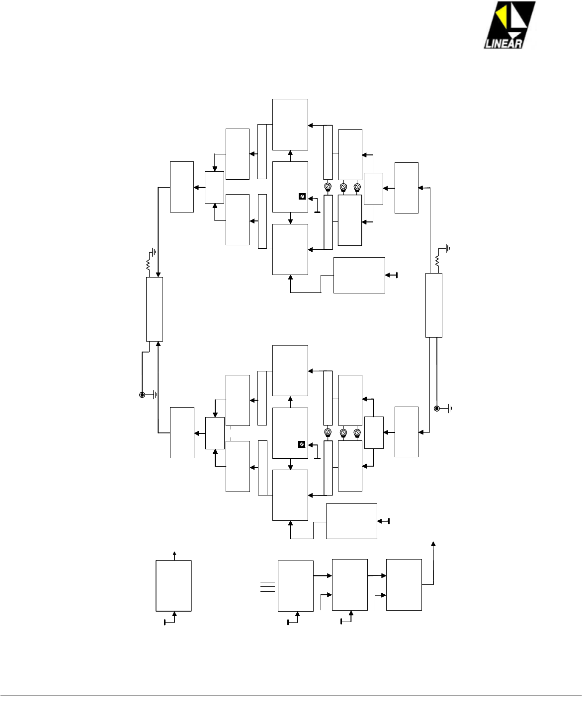
3.9.5. Module 4464 – PCB CIM3440 -16dB gain final 20W amplifier
This stage is built with 4 LDMOS transistors distributed in 2 cells of amplification. These 2 cells were designed on
push-pull class AB configuration, and than combined. The optimization process by band is also implemented.
The same PCB hardware is used for all 4 bands, the CIP8053. The nominal RF output power of each cell is
12.5W, totaling 20W following the output combiner. The overall gain of this stage is between 13dB and 16dB
depending on the assigned channel 6MHz UHF band.
AT7400 Owner Manual Rev. 2.0 – October 2006-10-23 Section 3 - 22/39
According with the Fig. 3.2: block diagram:
AMP LI FIER
A1 OU TPUT
(T1)
AMPLIFIER
A2 OUT PUT
(T1)
T1 GATE BIAS
(T P O - 1 )
FILTER
(L5)(C27)
(C22-C25)
+32V (VA)
AMPLIFIER
B1 OUT PUT
(T2 )
AMP L IF IE R
B2 OUT PUT
(T2)
T2GATE BIAS
(TPO-2)
RF I NP UT
FI LT ER
(L 10 )(C 57 )
(C53-C55)
+32V (VB)
INPUT
MATCHER
C9
C5 IN PUT
MATCHER
R F HYBR ID 50ȍ/10W
(R1 // R 2)
BALUN
DC BLOCKER
(C1)
RF O UTPUT
50ȍ/ 60W
(R11)
+ 12V
REGULATOR
(CI-4 )
+1 2V
+ 32V (VA)
DC
AMPLIFIER
(CI-3 )
THERMAL
SENSOR
(S1)
HISTERES E
COMPAR ATO R
(CI-3)
3dB C O UPL IN G
+12 V
+1 2V
+ 15V
+12 V
TEMPER ATU RE READI NG
OU T P UT
MATCHER
OU T P UT
MATC HER
OUT PUT
MATCHER
OUTP UT
MATCHE R
C13
IN PUT
MATCHER
C39
C35 INPUT
MATC HER
C43
TPO-1
T 1 ID ADJUST CURRENT : 60m V R39/ /R35
wi tho ut R F sig nal in put – AB cl ass
TPO-2
T 2 ID ADJUST CURRE NT : 60mV R36/ /R37
witho ut RF sig nal inp ut – AB cl ass
+1 2V +1 2V
(H C - 1 )
BA LUN
DC BL O C KE R
(C31)
BALUN
DC
BLOCKER
(C26)
BALUN
DC BLOCKER
(C56)
AMP LI FIER
A1 OU TPUT
(T1)
AMPLIFIER
A2 OUT PUT
(T1)
T1 GATE BIAS
(T P O - 1 )
FILTER
(L5)(C27)
(C22-C25)
FILTER
(L5)(C27)
(C22-C25)
+32V (VA)
AMPLIFIER
B1 OUT PUT
(T2 )
AMP L IF IE R
B2 OUT PUT
(T2)
T2GATE BIAS
(TPO-2)
RF I NP UT
FI LT ER
(L 10 )(C 57 )
(C53-C55)
+32V (VB)
INPUT
MATCHER
C9
C5 IN PUT
MATCHER
R F HYBR ID 50ȍ/10W
(R1 // R 2)
BALUN
DC BLOCKER
(C1)
BALUN
DC BLOCKER
(C1)
RF O UTPUT
50ȍ/ 60W
(R11)
+ 12V
REGULATOR
(CI-4 )
+1 2V
+ 32V (VA)
DC
AMPLIFIER
(CI-3 )
THERMAL
SENSOR
(S1)
HISTERES E
COMPAR ATO R
(CI-3)
3dB C O UPL IN G3dB C O UPL IN G
+12 V
+1 2V
+ 15V
+12 V
TEMPER ATU RE READI NG
OU T P UT
MATCHER
OU T P UT
MATC HER
OUT PUT
MATCHER
OUTP UT
MATCHE R
C13
IN PUT
MATCHER
C39
C35 INPUT
MATC HER
C43
TPO-1
T 1 ID ADJUST CURRENT : 60m V R39/ /R35
wi tho ut R F sig nal in put – AB cl ass
TPO-2
T 2 ID ADJUST CURRE NT : 60mV R36/ /R37
witho ut RF sig nal inp ut – AB cl ass
+1 2V +1 2V
(H C - 1 )
BA LUN
DC BL O C KE R
(C31)
BA LUN
DC BL O C KE R
(C31)
BALUN
DC
BLOCKER
(C26)
BALUN
DC
BLOCKER
(C26)
BALUN
DC BLOCKER
(C56)
BALUN
DC BLOCKER
(C56)
AT7400 Owner Manual Rev. 2.0 – October 2006-10-23 Section 3 - 23/39
3.9.5.1 RF Hybrid Input
This hybrid equally splits the incoming RF signal, keeping the input impedance at 50ȍlevel on an eventual
amplification cell malfunction. This hybrid is built out of 2 coupled transmission lines. In one end of the first
transmission line is connected the RF input signal, and on the other end a 50ȍ/10W (R1 parallel with R2) resistive
termination. On the ends of the second transmission line the coupled RF signal feeds the 2 amplification cells.
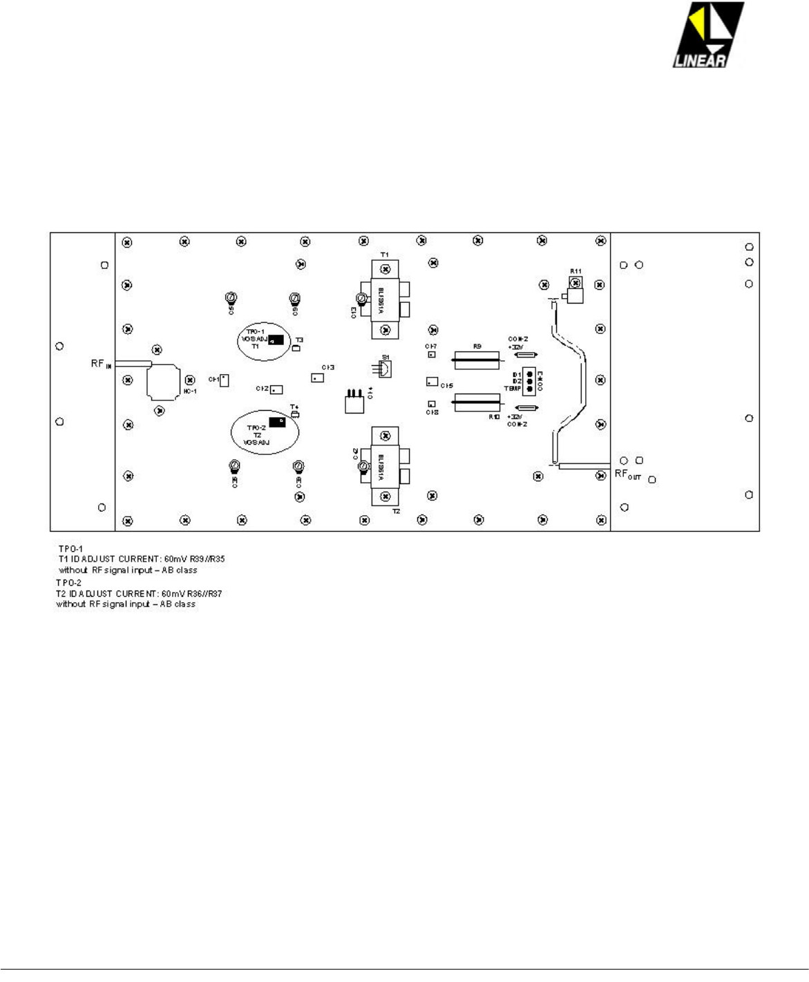
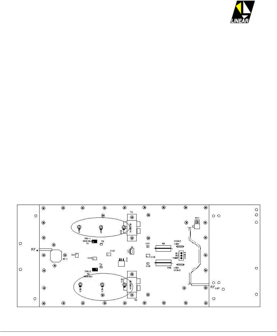
Fig.3.10: ID current adjust trim-pots location on PCB CIM 3440
3.9.5.2 UHF 12.5W Drive Amplifier – Cell A, Transistor T1
On this cell, the trim-pot TPO-1 at the same time adjusts the VGS1 voltage for T1, and the drained current ID.
Trimmers C5, C9 and C13, tunes and adjusts the input impedance. A combination among the trimmers’ physical
position and transmission lines’ length determines the bandwidth behavior. At the input, the capacitor C1 is a
input DC de-coupling, and at the output C26 as well.

AT7400 Owner Manual Rev. 2.0 – October 2006-10-23 Section 3 - 24/39
3.9.5.3 UHF 12.5W Driver Amplifier – Cell B, Transistor 2
On this cell, the trim-pot TPO-3 at the same time adjusts the VGS2 voltage for T2, and the drained current ID.
The trimmers C35, C39 and C43, tunes and adjusts the input impedance. A combination among the trimmers’
physical position and transmission lines’ length determines the bandwidth behavior. At the input, the capacitor
C31 is a input DC de-coupling, and at the output C56 as well.
3.9.5.4 Output Combiner
The 12.5W RF signals at the output of cells A and B are combined. The combination circuit is completed with the
absorber load, R11 (50ȍ/60W). R11 dissipates the extra power in case of failure of one cell, not disturbing the
output impedance on the cell that did not fail.
3.9.5.5 Temperature Alarm
The module 4464 is protected against high temperature levels. In case the internal temperature reaches or
exceeds 149°F, (65°C). The alarm circuitry is located at PCB CIM3440, and is composed by an thermal sensor
S1, by an integrated circuit CI-3. The temperature readings are DC converted and can be measure. This DC
voltage is routed directly to the pin #7 at the CON-6 at SCU (PCB CIM3297). If the module temperature exceeds
the limits on the module 4464, as consequence, the SCU will send a command to the sub-module 4456 that
disrupts the +32V to the module 4464.
AT7400 Owner Manual Rev. 2.0 – October 2006-10-23 Section 3 - 25/39
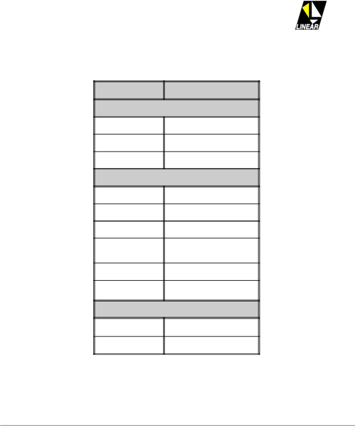
3.9.6. Module 4464 – PCB CIM3440 – Technical Specifications
FEATURE SPECIFICATION
INPUT
FREQUENCY 470 - 862MHz
IMPEDANCE 50 Ohms
RETURN LOSS ³22dB
OUTPUT
GAIN 13 TO 16dB
RF POWER UNTIL 20WRMS
HARMONICS £ -60dB
SPURIOUS
EMISSION < -54dB
INTERMODULATION < -46dB
IMPEDANCE 50 Ohms
GENERAL
VOLTAGE SUPPLY +32V
CONSUMPTION 12A (AB CLASS)
3.9.7. Module 4464 – PCB CIM3440- Adjustment Procedures
Always proceed to adjustment with the CIM3440 terminated by a 50ȍRF load, and make sure that there is no RF
signal present at the input of the module during the ID current adjustments.
AT7400 Owner Manual Rev. 2.0 – October 2006-10-23 Section 3 - 26/39
3.9.7.1 Drain Current ID, Adjustment
Turn the unit ON and wait 3 minutes for thermal stability. Use a good quality multi-meter able to read mVdc, avoid
to used auto-range multi-meters.
3.9.7.1.1. Transistor T1
1 - Set the trim-pot TPO-1 all way counterclockwise. On this condition no current flow over the transistor.
2 – Measure the voltage drop over R9. Set the multi-meter for 100mVdc full scale.
3 – Slowly start to turn the TPO-1 trim-pot clockwise up to the point one read 60mVdc over R9.
3.9.7.1.2. Transistor T2
1 – Set the trim-pot TPO-1 all way counterclockwise. On this condition no current flow over the transistor.
2 – Measure the voltage drop over R10. Set the multi-meter for 100mVdc full scale.
3 – Slowly start to turn the TPO-1 trim-pot clockwise up to the point one read 60mVdc over R10.
IMPORTANT: The amplifiers at CIM3440 are type class AB; the drain currents are dependent of the presence, or
not of the RF input signal. Higher the RF input signal, higher the ID current will be.
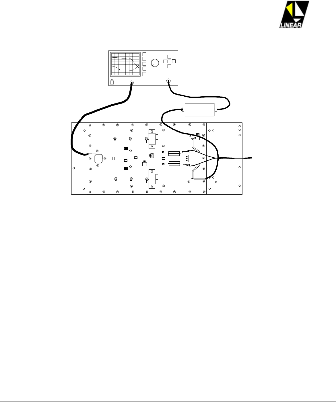
3.9.7.2 Module 4464 – PCB CIM3440 – Curve Response Adjustment
The module 4464 is a broadband UHF amplifier. The curve response is however optimized by band, ch14 to
ch25, ch25 to ch38, ch39 to ch53, and ch54 to ch69. The curve response optimization is factory performed and
should remain valid even an eventual LDMOS transistor replacement.
The cap trimmers are tuning point for the PCB, they should be tune seeking for best curve/gain response.
Fig.3.11: Cap trimmers location on PCB CIM 3440
AT7400 Owner Manual Rev. 2.0 – October 2006-10-23 Section 3 - 27/39
RF
OUT
.
.
C5
C9
C13
T1
C3 5
C42
C3 9
T2
CI
-
4
CI-2
TPO-2
T2
VG S ADJ
TPO-1
VG S ADJ
T1
CI-1
HC-1
R9
R10 +32V
CON-2
CON-2
+32V
CON
-
3
ID1
ID2
TEMP
R11
BLF861A
.
CI-3
S1
.
CI-5
.
CI-7
.
CI-8
T4
T3
RFIN
BLF861A
RF
IN
RF
OUT
NETWORK ANALYZER
30dB / 50W
ATTENU ATOR
+32V / 2A +32V / 2A
RF
OUT
.
.
C5
C9
C1 3
T1
C3 5
C42
C3 9
T2
CI
-
4
CI-2
TPO-2
T2
VG S ADJ
TPO-1
VG S ADJ
T1
CI-1
HC-1
R9
R10 +32V
CON-2
CON-2
+32V
CON
-
3
ID1
ID2
TEMP
R11
BLF861A
.
CI-3
S1
.
CI-5
.
CI-7
.
CI-8
T4
T3
RFIN
BLF861A
RF
OUT
..
..
C5
C9
C1 3
T1
C3 5
C4 2
C3 9
T2
CI
-
4
CI-2
TPO-2
T2
VG S ADJ
TPO-1
VG S ADJ
T1
CI-1
HC-1
R9R9
R10 +32V
CON-2
CON-2
+32V
CON
-
3
ID1
ID2
TEMP
R11
BLF861ABLF861A
..
CI-3
S1
..
CI-5
..
CI-7
..
CI-8
T4
T3
RFIN
BLF8 61A
BLF861A
RF
IN
RF
OUT
NETWORK ANALYZER
30dB / 50W
ATTENU ATOR
+32V / 2A +32V / 2A
MODULE 4464
Fig. 3.12: Suggested gain and curve response evaluation for PCB CIM3440
The network analyzer level should be set upfront for -20dBm at the assigned UHF channel band. Monitor the
results at the output of the PCB CIM3440. Tune the cap trimmers for best curve response, flat shape inside the
band. Watch the gain according with the indication below:
x16dB – Band 1: ch14 to ch25.
x15dB – Band 2: ch26 to ch38.
x15dB – Band 3: ch39 to ch53.
x14dB – Band 4: ch54 to ch69.
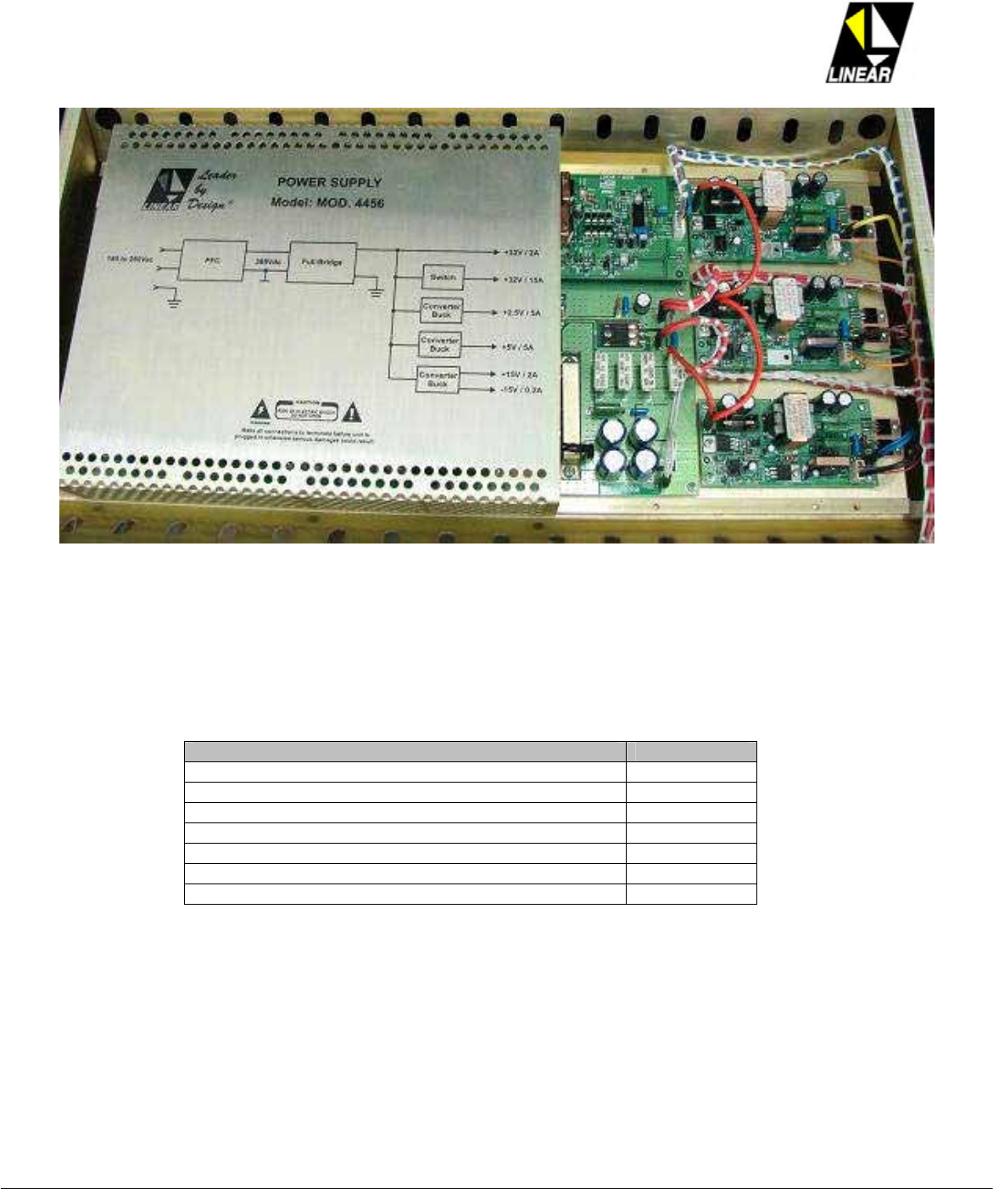
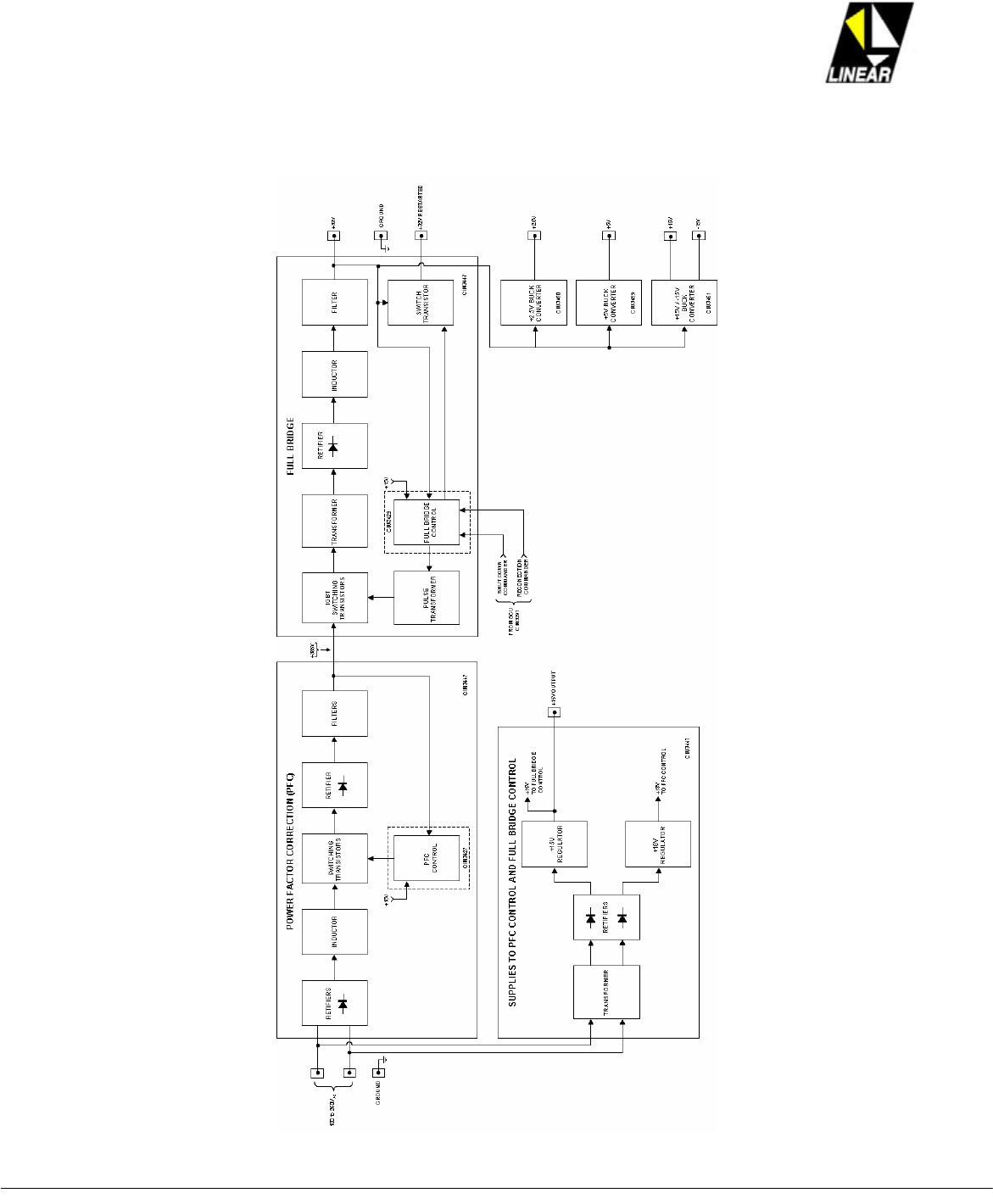
3.10. Module 4456 – 60A Multiple Power Supply
In the ADVANCED TV line all DC power supplies uses a switching technology, type full-bridge powered by 208 up
to 240 Vac, showing overall efficiency above 80%. As part of the power supply design, there is a power factor
corrector, PFC, circuit. Besides correct the power factor to close to 1, this circuit also contributes to reduce the
harmonic content returning from the unit into the AC mains.
AT7400 Owner Manual Rev. 2.0 – October 2006-10-23 Section 3 - 28/39
Fig. 3.13: Module 4456 – 60A multiple power supply
The module 4456 generates the following voltage values for this drawer internal use only:
Voltage Current
+32V Fixed 2A
+32V ON/OFF according to command. 15A
+15V Direct 1A
+15V 2A
-15V 200 mA
+5V 5 A
+2.5V 5 A
Table 2 - Module 4456: Listing of Voltage and current, per each power supply.
The multiple power supply module 4456 is composed by the following PCB’s:
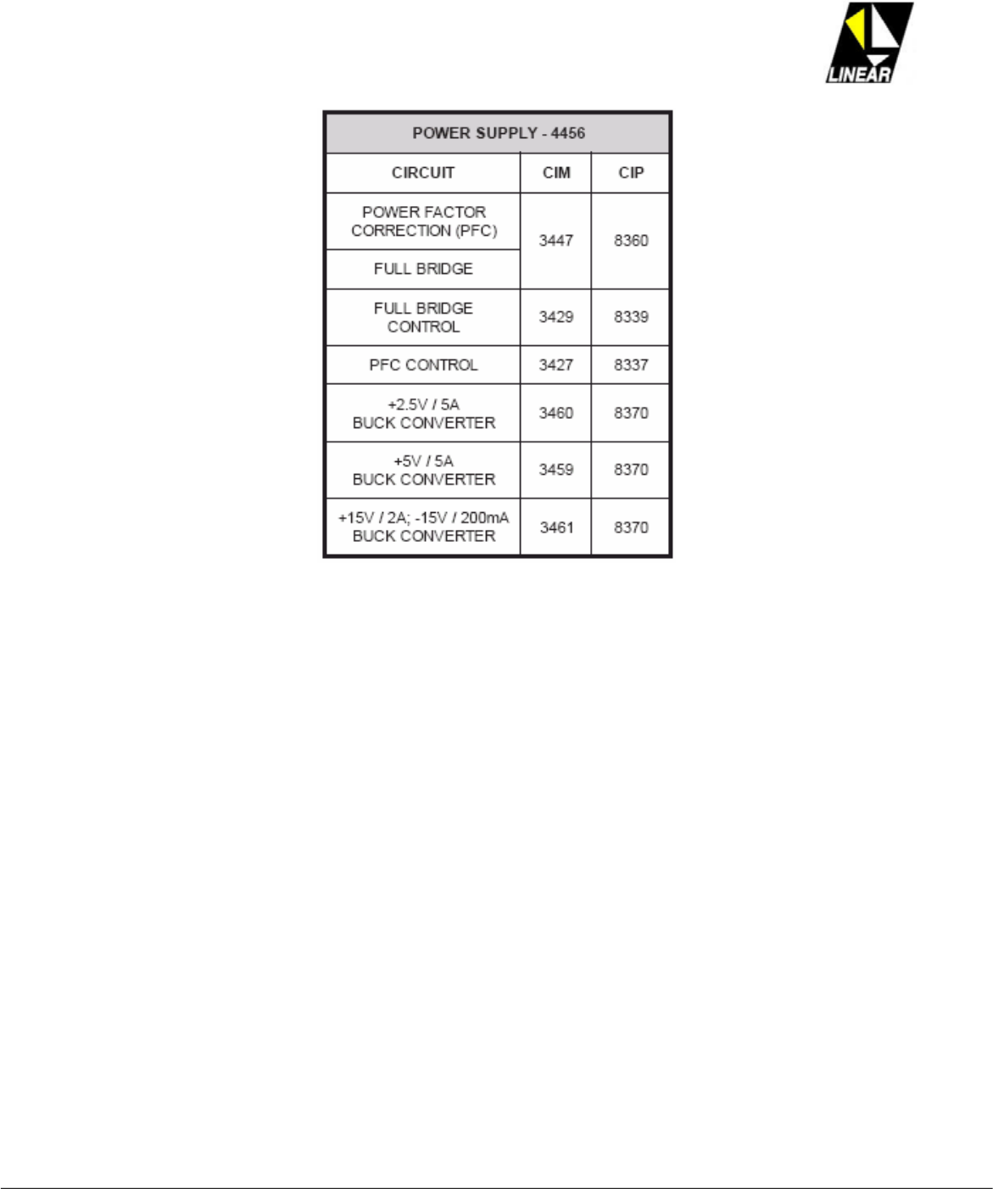
AT7400 Owner Manual Rev. 2.0 – October 2006-10-23 Section 3 - 29/39
Fig. 3.13: Module 4456 - Circuit functions: electrical schematic diagram, (CIM), and printed circuit board, (CIP).
AT7400 Owner Manual Rev. 2.0 – October 2006-10-23 Section 3 - 30/39
3.10.1. Module 4456 – Block Diagram