Hitachi Nji 350B Users Manual HIDIC MICRO EH APPLICATION
NJI-350B micro-EH-MA-NJI350BX-W
NJI-350B to the manual b0c219f7-c5b8-45bc-99ca-fbfc487bf68c
2015-01-24
: Hitachi Hitachi-Nji-350B-Users-Manual-314269 hitachi-nji-350b-users-manual-314269 hitachi pdf
Open the PDF directly: View PDF ![]() .
.
Page Count: 319 [warning: Documents this large are best viewed by clicking the View PDF Link!]
- HIDIC MICRO-EH
- About a guarantee
- Safety Precautions
- Revision History
- Table of Contents
- Chapter 1 Features
- Chapter 2 System Overview
- Chapter 3 Function and Performance Specifications
- 3.1 General Specifications
- 3.2 Function Specifications
- 3.3 Performance Specifications
- 3.3.1 Calculation Specifications
- 3.3.2 Input Specifications
- 3.3.3 Output Specifications
- 3.3.4 High-Speed Counter Specifications
- 3.3.5 PWM Output/Pulse Array Output Specifications
- 3.3.6 Analogue Input Specifications
- 3.3.7 Analogue Output Specifications
- 3.3.8 Potentiometer Analogue Input Specifications
- 3.3.9 Interrupt Input Specifications
- 3.3.10 Backup
- 3.3.11 Expansion
- 3.3.12 Clock Function
- 3.3.13 Power Supply for Sensor
- Chapter 4 Product lineup and wiring
- Chapter 5 Instruction Specifications
- Chapter 6 I/O Specifications
- Chapter 7 Programming
- Chapter 8 High-speed counter, PWM / Pulse train output and Analogue I/O
- Chapter 9 PLC operation
- Chapter 10 PLC Installation, Mounting, Wiring
- Chapter 11 Communication Specifications
- Chapter 12 Error Code List and Special Internal Outputs
- Chapter 13 Troubleshooting
- Chapter 14 Operation Examples
- Chapter 15 Daily and Periodic Inspections
- Appendix 1 H-Series Instruction Support Comparison Chart
- Appendix 2 Standards

HITACHI PROGRAMMABLE CONTROLLER
APPLICATION MANUAL
NJI-350B (X)

WARNING
To ensure that the equipment described by this manual. As well as all equipment connected to and used
with it, operate satisfactorily and safely, all applicable local and national codes that apply to installing and
operating the equipment must be followed. Since codes can vary geographically and can change with
time, it is the user’s responsibility to determine which standard and codes apply, and to comply with
them.
FAILURE TO COMPLY WITH APPLICABLE CODES AND STANDARDS CAN RESULT IN
DAMAGE TO EQUIPMENT AND / OR SERIOUS INJURY TO PERSONNEL.
INSTALL EMERGENCY POWER STOP SWITCH WHICH OPERATES INDEPENDENTLY OF
THE PROGRAMMABLE CONTROLLER TO PROTECT THE EQUIPMENT AND / OR
PERSONNEL IN CASE OF THE CONTROLLER MALFUNCTION.
Personnel who are to install and operate the equipment should carefully study this manual and any
others referred to by it prior to installation and / or operation of the equipment. Hitachi, Ltd. constantly
strives to improve its products, and the equipment and the manual(s) that describe it may be different
from those already in your possession.
If you have any questions regarding the installation and operation of the equipment, or if more
information is desired, contact your local Authorized Distributor or Hitachi, Ltd.
IMPORTANT
THIS EQUIPMENT GENERATES, USES, AND CAN RADIATE RADIO FREQUENCY ENERGY AND, IF
NOT INSTALLED AND USED IN ACCORDANCE WITH THE INSTRUCTION MANUAL, MAY CAUSE
INTERFERENCE TO RADIO COMMUNICATIONS. AS TEMPORARILY PERMITTED BY REGULATION,
IT HAS NOT BEEN TESTED FOR COMPLIANCE WITH THE LIMITS FOR CLASS A COMPUTING
DEVICES PURSUANT TO SUBPART J OF PART 15 OF FCC RULES, WHICH ARE DESIGNED TO
PROVIDE REASONABLE PROTECTION AGAINST SUCH INTERFERENCE.
OPERATION OF THIS EQUIPMENT IN A RESIDENTIAL AREA IS LIKELY TO CAUSE INTERFERENCE
IN WHICH CASE THE USER, AT HIS OWN EXPENSE, WILL BE REQUIRED TO TAKE WHATEVER
MEASURES MAY BE REQUIRED TO CORRECT THE INTERFERENCE.

LIMITED WARRANTY AND IMITATION OF LIABILITY
Hitachi, Ltd. (Hitachi) warrants to the original purchaser that the programmable controller (PLC)
manufactured by Hitachi is free from defects in material and workmanship under normal use and
service. The obligation of Hitachi under this warranty shall be limited to the repair or exchange of any
part or parts which may prove defective under normal use and service within eighteen (18) months from
the date of manufacture or twelve (12) months from the date of installation by the original purchaser
which ever occurs first, such defect to be disclosed to the satisfaction of Hitachi after examination by
Hitachi of the allegedly defective part or parts. This warranty in expressly in lieu of all other warranties
expressed or implied including the warranties of merchantability and fitness for use and of all other
obligations or liabilities and Hitachi neither assumes, nor authorizes any other person to assume for
Hitachi, any other liability in connection with the sale of this PLC. This warranty shall not apply to this
PLC or any part hereof which has been subject to accident, negligence, alteration, abuse, or misuse.
Hitachi makes no warranty whatsoever in respect to accessories or parts not supplied by Hitachi. The
term "original purchaser", as used in this warranty, shall be deemed to mean that person for whom the
PLC in originally installed.
In no event, whether as a result of breach of contract, warranty, tort (including negligence) or otherwise,
shall Hitachi or its suppliers be liable for any special, consequential, incidental or penal damages
Including, but not limited to, loss of profit or revenues, loss of use of the products or any associated
equipment, damage to associated equipment, cost of capital, cost of substitute products, facilities,
services or replacement power, down time costs, or claims of original purchaser’s customers for such
damages.
To obtain warranty service, return the product to your distributor, or send it with a description of the
problem, proof of purchase, post paid, insured, and in a suitable package to:
Quality Assurance Dep.
Hitachi Industrial Equipment Systems Co., Ltd.
46-1, Ooaza-Tomioka Nakajo-machi
Kitakanbara-gun, Niigata-ken
959-2608 JAPAN
Copyright 2000 by Hitachi Industrial Equipment Systems Co., Ltd.
All Rights reserved - Printed in Japan
The information and/or drawings set forth in this document and all rights in and to inventions disclosed herein and
patents which might be granted thereon disclosing or employing and the materials, techniques or apparatus described
herein are the exclusive property of Hitachi, Ltd.
No copies of the information or drawings shall be made without the prior consent of Hitachi, Ltd.
Hitachi, Ltd. provides customer assistance in varied technical areas. Since Hitachi does not posses full access to data
concerning all of the uses and applications of customer‘s products, responsibility is assumed by Hitachi neither for
customer product design nor for any infringements of patents or rights of others which may result from Hitachi
assistance.
The specifications and descriptions contained in this manual were accurate at the time they were approved for printing.
Since Hitachi, Ltd. Incorporated constantly strives to improve all its products, we reserve the right to make changes to
equipment and/or manuals at any time without notice and without incurring any obligation other than as noted in this
manual.
Hitachi, Ltd. assumes no responsibility for errors that may appear in this manual.
As the product works with user program and Hitachi, Ltd. cannot test all combination of user program components, it is
assumed that a bug or bugs may happen unintentionally. If it is happened: please inform the fact to Hitachi, Ltd. or its
representative. Hitachi will try to find the reason as much as possible and inform the countermeasure when obtained.
Nevertheless Hitachi, Ltd. intends to make products with enough reliability, the product has possibility to be damaged at
any time. Therefore personnel who are to install and operate the equipment has to prepare with the counter-measure such
as power off switch can be operated independently of the controller. Otherwise, it can result in damage to equipment
and/or serious injury to personnel.
Safety Precautions
Read this manual and attached documents thoroughly before installing and operating this unit, and performing
maintenance or inspection of this unit in order to use the unit correctly. Be sure to use this unit after acquiring adequate
knowledge of the unit, all safety information, and all precautionary information. Also, be sure to deliver this manual to
the person in charge of maintenance.
Safety caution items are classified as “Danger” and “Caution” in this document.
DANGER : Cases in which, if handled incorrectly, a dangerous situation may occur, resulting in
possible death or severe injury.
CAUTION : Cases in which, if handled incorrectly, a dangerous situation may occur, resulting in
possible minor to medium injury to the body, or only mechanical failure.
However, depending on the situation, items marked with may result in major accidents.
Both of these items contain important safety information, so be sure to follow them closely.
Icons for prohibited items and required items are shown below:
: Indicates a prohibited item (item that cannot be performed). For example, when open flames are prohibited,
is shown.
: Indicates a required item (item that must be performed). For example, when grounding must be performed,
is shown.
1. Installation
CAUTION
•Use this product in an environment as described in the catalogue and this document.
If this product is used in an environment subject to high temperature, high humidity, excessive dust, corrosive
gases, vibration or shock, it may result in an electric shock, fire or malfunction.
•Installation this product according to the instructions in this manual.
If installation is not performed correctly, it may result in falling, malfunction, or an operational error of the unit.
•Never allow foreign objects such as wire chips to enter the unit.
They may cause a fire, malfunction, or failure.
CAUTION
2. Wiring
REQUIRED
•Always perform grounding (FE terminal).
If grounding is not performed, there is a risk of an electric shock or malfunction.
CAUTION
•Connect a power supply that meets the rating.
If a power supply that does not meet the rating is connected, it may result in a fire.
•Any wiring operation should only be performed by a qualified technician.
If wiring is performed incorrectly, it may result in a fire, failure, or electric shock.
3. Precautions When Using the Unit
DANGER
•Never touch the terminals while the power is on.
There is a risk of an electric shock.
•Configure the emergency stop circuit, interlock circuit and other related circuits external to the programmable
controller (referred to as the PLC in this document).
Otherwise, a failure in the PLC may damage the equipment or result in a serious accident.
Never interlock the unit with the external load via the relay drive power supply of the relay output module.
CAUTION
•Before performing program change, forced output, run, stop and other operations while the unit is in operation, be
sure to check the validity of the applicable operation and safety.
An operation error may damage the equipment or result in a serious accident.
•Be sure to power on the unit according to the designated power-on sequence.
Otherwise, an erroneous operation may damage the equipment or result in a serious accident.

4. Maintenance
DANGER
•Never connect the and of the battery in reverse. Also, never charge, disassemble, heat, place in fire, or
short circuit the battery.
There is a risk of an explosion or fire.
PROHIBITED
•Never disassemble or modify the unit.
These actions may result in a fire, malfunction, or failure.
CAUTION
•Be sure to turn off the power supply before removing or attaching the module/unit.
Otherwise, it may result in an electric shock, malfunction, or failure.

Revision History
No. Description of Revision Date of Revision Manual Number
1 Appendix-1 Instruction Support
FUN92 to 96 of H-4010 { -> ×.
Appendix-2 Task code H28
Corrected explanation of Timer counter number.
2000/11 NJI-350 (X)
2 Postscript of battery error detection. (3.2 chapters item
number 26, 15 chapters (4) )
Correct a description of digital filter . (8.7 chapters)
Addition of appendix 3.
2000/12 NJI-350A (X)
3 28 points expansion units added.
Analog expansion module added.
Circuit diagram added in chapter 3
FUN 5, TRNS/RECV command added in chapter 5.
2003/10 NJI-350B (X)

Table of Contents
Chapter 1 Features ..................................................................................................................................... 1-1 to 1-2
Chapter 2 System Overview....................................................................................................................... 2-1 to 2-2
Chapter 3 Function and Performance Specifications ............................................................................... 3-1 to 3-14
3.1 General Specifications ............................................................................................................. 3-1
3.2 Function Specifications............................................................................................................ 3-2
3.3 Performance Specifications...................................................................................................... 3-6
3.3.1 Calculation Specifications ............................................................................................ 3-6
3.3.2 Input Specifications ...................................................................................................... 3-7
3.3.3 Output Specifications.................................................................................................... 3-8
3.3.4 High-Speed Counter Specifications ............................................................................ 3-12
3.3.5 PWM Output/Pulse Train Output Specifications........................................................ 3-12
3.3.6 Analogue Input Specifications .................................................................................... 3-12
3.3.7 Analogue Output Specifications ................................................................................. 3-13
3.3.8 Potentiometer Analogue Input Specifications............................................................. 3-14
3.3.9 Interrupt Input Specifications ..................................................................................... 3-14
3.3.10 Backup........................................................................................................................ 3-14
3.3.11 Expansion ................................................................................................................... 3-14
3.3.12 Clock Function............................................................................................................3-15
3.3.13 Power Supply for Sensor ............................................................................................ 3-16
Chapter 4 Product lineup and wiring ....................................................................................................... 4-1 to 4-18
4.1 Product lineup.......................................................................................................................... 4-1
4.2 10-Point Basic Unit.................................................................................................................. 4-3
4.3 14-Point Basic Unit.................................................................................................................. 4-4
4.4 23-Point and 28-Point Basic Unit ............................................................................................ 4-5
4.5 Expansion Unit......................................................................................................................... 4-6
4.6 Terminal Layout and Wiring.................................................................................................... 4-7
4.7 Weights and Power Consumption .......................................................................................... 4-16
4.8 Exterior Dimensions .............................................................................................................. 4-17
Chapter 5 Instruction Specifications......................................................................................................5-1 to 5-146
5.1 Instruction Classifications ........................................................................................................ 5-1
5.2 List of Instructions ................................................................................................................... 5-2
5.3 Instruction Specification Details ............................................................................................5-13
Chapter 6 I/O Specifications...................................................................................................................... 6-1 to 6-6
6.1 I/O Assignment ........................................................................................................................ 6-2
6.2 External I/O Numbers .............................................................................................................. 6-3
6.3 Internal Output Numbers.......................................................................................................... 6-6

Chapter 7 Programming............................................................................................................................. 7-1 to 7-8
7.1 Memory Size and Memory Assignment ................................................................................... 7-1
7.2 Programming Devices.............................................................................................................. 7-2
7.3 Programming Methods............................................................................................................. 7-3
7.4 Program Transfer ..................................................................................................................... 7-7
Chapter 8 High speed counter, PWM/Pulse train output and Analogue I/O............................................ 8-1 to 8-22
8.1 Input/Output Function.............................................................................................................. 8-1
8.1.1 Initial Setting for Input/Output Function ...................................................................... 8-1
8.1.2 Operation Mode............................................................................................................ 8-2
8.1.3 Input/Output Setting .................................................................................................... 8-3
8.1.4 Input/Output Setting (Mode 10) ................................................................................... 8-4
8.1.5 Special Output Operation in CPU STOP Status ........................................................... 8-5
8.1.6 Pulse / PWM Output adjustment................................................................................... 8-5
8.2 High-Speed Counter (Single-Phase) ........................................................................................ 8-6
8.2.1 Operation of Single-Phase Counter............................................................................... 8-6
8.2.2 Setting of Single-Phase Counter ................................................................................... 8-8
8.3 High-Speed Counter (Two-Phase Counter)............................................................................ 8-10
8.3.1 Operation of the Two-Phase Counters........................................................................ 8-10
8.3.2 Setting of Two-Phase Counter .................................................................................... 8-13
8.4 PWM Output.......................................................................................................................... 8-15
8.4.1 Operation of PWM Output ......................................................................................... 8-15
8.4.2 Setting of PWM Output .............................................................................................. 8-16
8.5 Pulse Train Output ................................................................................................................. 8-18
8.5.1 Operation of Pulse Output .......................................................................................... 8-18
8.5.2 Setting of Pulse Output ............................................................................................... 8-19
8.6 Interrupt Input ........................................................................................................................ 8-21
8.7 Digital Filter........................................................................................................................... 8-21
8.8 Potentiometers........................................................................................................................ 8-22
8.9 Analogue Input....................................................................................................................... 8-23
8.10 Analogue Output .................................................................................................................... 8-23
8.11 Analogue Expansion unit ....................................................................................................... 8-24
Chapter 9 PLC Operation ........................................................................................................................ 9-1 to 9-12
9.1 RUN Start ................................................................................................................................ 9-2
9.1.1 Normal Scan ................................................................................................................. 9-3
9.1.2 Periodical Scan ............................................................................................................. 9-5
9.1.3 Interrupt scan ................................................................................................................ 9-6
9.1.4 Relationship of Each Scan Type................................................................................... 9-8
9.2 Online Change in RUN ............................................................................................................ 9-9
9.3 Instantaneous Power Failure ..................................................................................................9-10
9.4 Operation Parameter .............................................................................................................. 9-11
9.5 Test Operation........................................................................................................................ 9-12
9.6 Forced Set/Reset .................................................................................................................... 9-12
9.7 Forced Output ........................................................................................................................ 9-12

Chapter 10 PLC Installation, Mounting, Wiring...................................................................................... 10-1 to 10-8
10.1 Installation ............................................................................................................................. 10-1
10.2 Wiring .................................................................................................................................... 10-3
Chapter 11 Communication Specifications............................................................................................ 11-1 to 11-10
11.1 Port function .......................................................................................................................... 11-1
11.2 Port 1...................................................................................................................................... 11-1
11.3 Port 2...................................................................................................................................... 11-3
11.4 General purpose port (Port 1,2) ............................................................................................. 11-4
11.5 Modem Control Function....................................................................................................... 11-5
11.5.1 Configuration.............................................................................................................. 11-5
11.5.2 AT Commands............................................................................................................ 11-5
11.6 Connecting to the Ports .......................................................................................................... 11-8
11.6.1 Port 1 .......................................................................................................................... 11-8
11.6.2 Port 2 .......................................................................................................................... 11-9
Chapter 12 Error Code List and Special Internal Outputs ..................................................................... 12-1 to 12-14
12.1 Error Codes............................................................................................................................ 12-1
12.2 Syntax and Assembler Error Codes........................................................................................ 12-3
12.3 Operation Error Codes ........................................................................................................... 12-4
12.4 Bit Special Internal Output Area............................................................................................ 12-5
12.5 Word Special Internal Output Area........................................................................................ 12-9
Chapter 13 Troubleshooting .................................................................................................................. 13-1 to 13-16
13.1 Error Display and Actions...................................................................................................... 13-1
13.2 Checklist when Abnormality Occurred .................................................................................. 13-5
13.3 Procedures to Solve Abnormality .......................................................................................... 13-6
Chapter 14 Operation Examples ............................................................................................................ 14-1 to 14-16
Chapter 15 Daily and Periodic Inspections.............................................................................................. 15-1 to 15-2
Appendix 1 H-Series Instruction Support Comparison Chart.................................................................................A-1
Appendix 2 Standards...........................................................................................................................................A-11
MEMO

Chapter 1 Features
1-1
Chapter 1 Features
1. Multifunctional all-in-one type PLC
The MICRO-EH is a multifunctional all-in-one type PLC that contains all necessary parts—a power supply and
CPU parts as well as I/O units--within one unit.
Three sizes of PLCs are available: 10, 14, and 28 points. A type with 23 points plus three points of analog I/O
having the same size as the 28-point PLC is also available. Moreover, for PLCs with more than 14 points, it is
possible to install additional 14 or 28 point expansion units up to four units. Thus, the MICRO-EH can control a
wide range of systems from small to medium size.
2. Simplified positioning by counter inputs and pulse train outputs
The function of inputs/outputs can be selected from four modes. By selecting a mode, inputs/outputs that are used as
normal inputs/outputs can be set as counter inputs and pulse train outputs. Through a combination of these special
inputs/outputs, it is possible to control positioning without using special modules.
3. Simplified instrument system by analog integration
For the 23-point PLC, there are two points of analog input and one point of analog output for which both current
and voltage can be selected. High performance analog channels, with a resolution of 12 bits and an overall accuracy
of ±1 % or less, can be used without requiring special settings of the channels; thus, a simplified instrument system
can easily be implemented.
4. Superior upward compatibility
The MICRO-EH has been developed as a part of the EH/H series family.
Debugging and programming can be performed using the same concept as for the EH/H series.
In addition, the MICRO-EH software property can effectively be applied to the EH/H series for future system
expansion.
5. Easy maintenance through removable terminal blocks and installation on a DIN rail
All models of the MICRO-EH series support the DIN rail so that the PLC can easily be mounted and dismounted. In
addition, the I/O section of the 14-point PLC or more utilizes a removable terminal block. Thus, erroneous and
faulty wiring that may occur when connecting to external devices can be reduced.
6. Remote maintenance through modem connection
Communication with remote sites can be performed via dial-up line by connecting a modem to port 1 on the 14-
point PLC or more of the MICRO-EH series. It is possible to monitor and manage remote systems from an office or
monitor room.
7. Easily adjustable potentiometer
The 14-point PLC or more of the MICRO-EH series supports two potentiometers.
By using these potentiometers, it is possible to rewrite internal output values in real-time by one driver without using
peripheral devices. Since the resolution of the potentiometer is 10 bits, it is possible to set any value from 0 to 3FFH.
To obtain stable analog values of the potentiometers, it is possible to sample 1 to 40 analog values of the
potentiometers and average them.
8. Maintaining programs without a battery
It is possible to retain user programs in case of out-of battery or no battery, since FLASH memory is used as the
backup memory for the user programs. However, a battery is necessary for data memory backup. (See the Notes in
Chapter 7.1 for a list of precautionary details.)
9. Support for various programming languages
The MICRO-EH supports “Pro-H,” the programming software that allows creating programs in five programming
languages regulated in IEC1131-3. This means that customers who have learned languages other than Ladder can
easily create programs with this programming software.
10. Compliant with overseas specifications as standard
All types of MICRO-EH PLCs have obtained the CE mark, C-TICK and UL. Therefore, systems in which these
PLCs are installed can be exported without requiring any modification.

Chapter 1 Features
1-2
MEMO
Chapter 2 System Overview
2-1
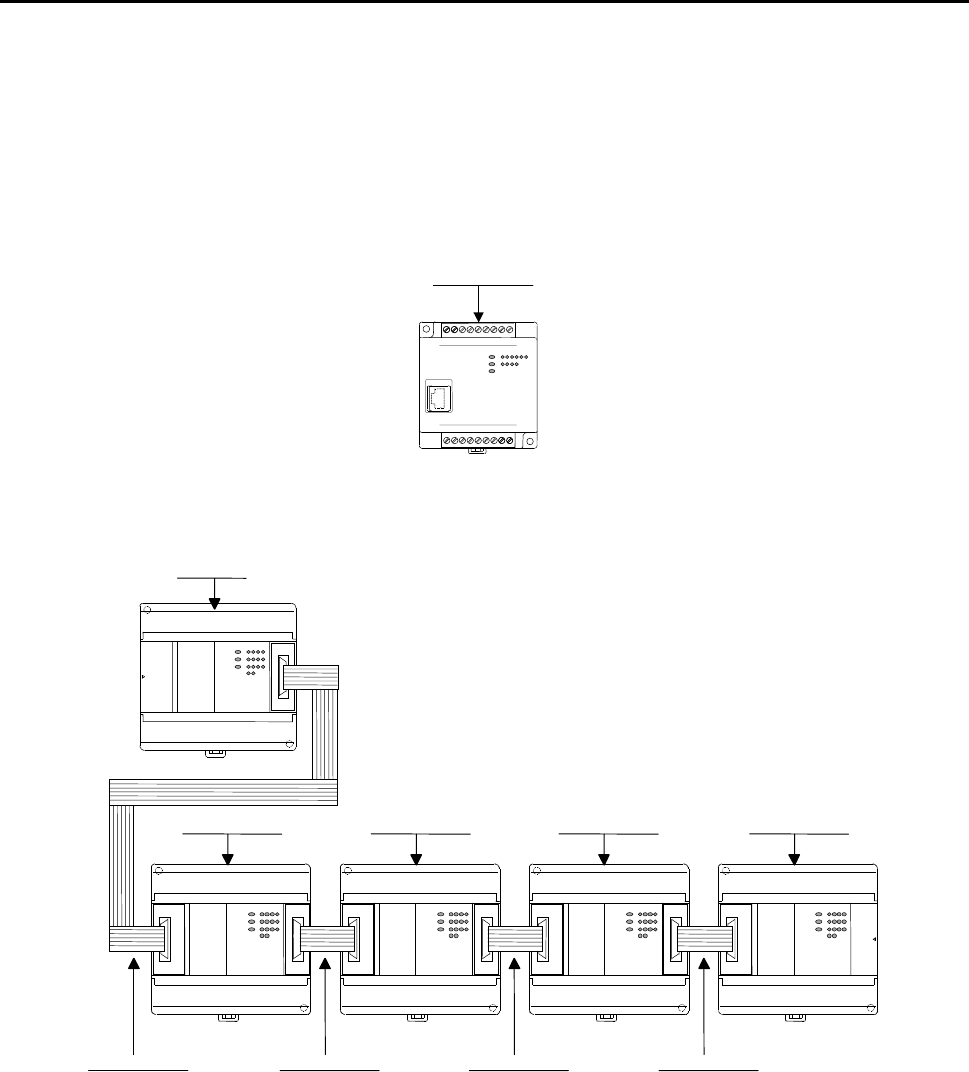
Chapter 2 System Overview
This chapter describes the system configuration of the MICRO-EH.
The MICRO-EH is an all-in-one type programmable controller, and has the following system configuration.
Figure 2.1 10-point type system configuration diagram
Figure 2.2 14-point type system configuration diagram
1] Basic unit
1] Basic unit
3] Expansion cable3] Expansion cable3] Expansion cable3] Expansion cable
2] Expansion unit2] Expansion unit2] Expansion unit2] Expansion unit
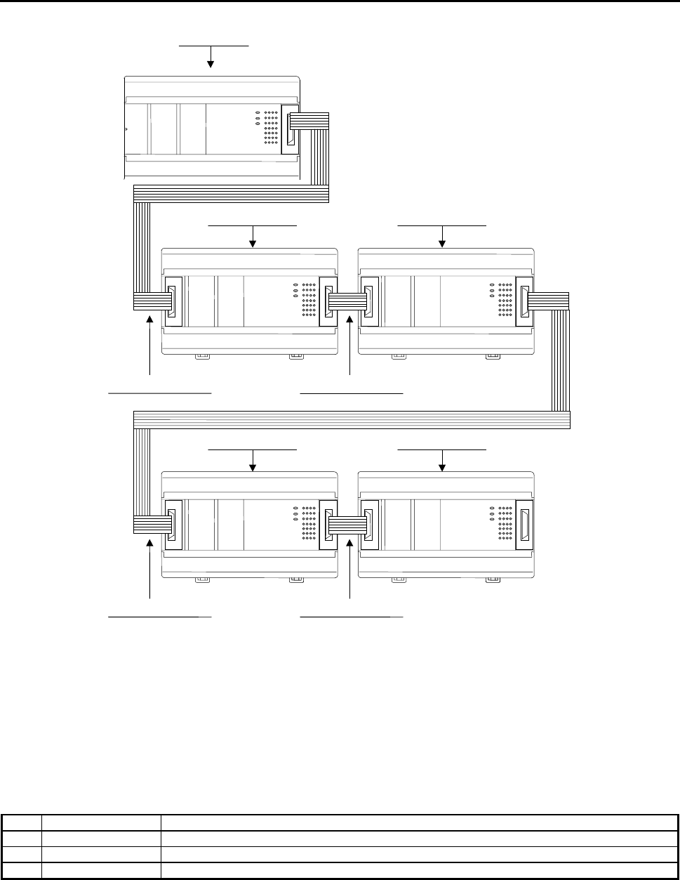
Chapter 2 System Overview
2-2
[1] Basic unit
[2] Expansion unit
[3] Expansion cable
[2] Expansion unit
[2] Expansion unit [2] Expansion unit
[3] Expansion cable
[3] Expansion cable [3] Expansion cable
Figure 2.3 23,28-point type system configuration diagram
No restriction for combination of 14,23,28 points, and basic/expansion unit.
14 points basic unit can handle any type of expansion units, and 23/28 points basic unit as well.
No. Device name Description
1] Basic unit Calculates, imports inputs, and controls outputs according to the contents of user programs.
2] Expansion unit 14 points digital unit, 4 in/2 out analog unit
3] Expansion cable Cable for connecting the basic unit and expansion unit, or between expansion units.

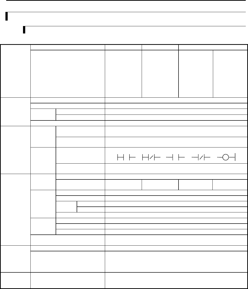
Chapter 3 Function and Performance Specifications
3-1
Chapter 3 Function and Performance
Specifications
3.1 General Specifications
Item Specification
Power supply type AC DC
Power voltage 100/110/120 V AC (50/60 Hz),
200/220/240 V AC (50/60 Hz)
24 V DC
Power voltage fluctuation
range
85 to 264 V AC wide range 19.2 to 30 V DC
Current consumption Please refer to 4.7, “Weights and Power Consumption.”
Allowable momentary power
failure
85 to 100 V AC: For a momentary power
failure of less than 10 ms,
operation continues
100 to 264 V AC: For a momentary power
failure of less than 20 ms,
operation continues
19.2 to 30 V DC: For a momentary power
failure of less than 10 ms,
operation continues
Operating ambient temp. 0 to 55 °C
Storage ambient temp. -10 to 75 °C
Operating ambient humidity 5 to 95 % RH (no condensation)
Storage ambient humidity 5 to 95 % RH (no condensation)
Vibration proof Conforms to JIS C 0911
Noise resistance {Noise voltage 1,500 Vpp Noise pulse width 100 ns, 1 µs
(Noise created by the noise simulator is applied across the power supply module's input
terminals. This is determined by our measuring method.)
{Based on NEMA ICS 3-304
{Static noise: 3,000 V at metal exposed area
{Conforms with EN50081-2 and EN50082-2
Supported standards Conforms with UL, CE markings and C-TICK
Insulation resistance 20 MΩ or more between the AC external terminal and the protection earth (PE) terminal (based
on 500 V DC mega)
Dielectric withstand voltage 1,500 V AC for one minute between the AC external terminal and the protection earth (PE)
terminal
Grounding Class D dedicated grounding (grounded by a power supply module)
Environment used No corrosive gases and no excessive dirt
Structure Attached on an open wall
Cooling Natural air cooling

Chapter 3 Function and Performance Specifications
3-2
3.2 Function Specifications
The functions available in the MICRO-EH are described in the table below.
No. Item Description
1 Basic functions The following functions can be executed when constructing a system using the PLC.
1] An input signal is received from the control object, operations are performed according to
the contents of the program created by the user and the results are output as an output signal.
Also, operation results and progress information can be retained in the internal output area.
2] Power is supplied to the main module, system starts to run, and the operation described
above is performed continuously until the power is shut down or the system stops running.
3] The information retained internally can be extracted by a device connected externally or can
be set in other information. Also, this information is initialized at the time the system starts
running, but it can also be retained depending on the user settings.
4] Operating status can be confirmed with the LED display of each unit or with an external
device that has been connected.
2 Setting and display The following have been provided for the user to set or confirm various types of operation
status:
1] DIP switch (basic unit)
This specifies the CPU communication function setting and operation mode, etc. (except for
10-point type)
2] RUN switch (basic unit)
It can instruct to run and stop. (external input for 10-point type)
3] LED display (basic unit and expansion unit)
Indicates the power system status, operating status and I/O operation status.
4] Communication connector (basic unit)
This can connect external devices using RS-232C, RS-485, RS-422. (only the 23-point and
28-point types with RS-485, RS-422)
5] Expansion connector (basic unit and expansion unit)
This allows installation of additional input/output. (except for 10-point type)
6] Terminal block (basic unit and expansion unit)
This performs the connections for supplying power, and for handling signals with the
control object.
3 Number of I/O points The number of points that can be controlled with respect to the control object is as follows:
1] External inputs/outputs
The number of points that can be use for external inputs/outputs differs depending on the
basic unit. The 10-point type cannot expand the inputs/outputs. For the 14-point, 23-point
and 28-point types, a maximum of 4 expansion units can be connected. The I/O numbers for
inputs are indicated by X, WX, DX and outputs are indicated by Y, WY, DY.
2] Internal outputs
These are areas for temporarily storing information. The I/O numbers include M, WM, DM,
R, WR, DR.
3] A timer counter is provided internally.
4] Array (corresponding to a substitution statement only)
An array of I/O numbers can be expressed by enclosing by parentheses.
4 User program
memory
The program in which the control contents have been described can be stored. This FLASH
memory resides in the basic unit.
1] The contents of this memory will be maintained even if the power is shut off. Because of
this, it is necessary to initialize the memory since it may have undefined after the unit is
purchased.
2] Programming is done using peripheral units such as programming software (LADDER
EDITOR) for the H-series programmable controllers.
3] The instructions that can be used are those designated by the H-series ladder. See the list of
instructions for details.
4] A battery is not required to retain the contents of the user program. Always save the created
programs to a floppy disk just in case an unexpected problem occurs.

Chapter 3 Function and Performance Specifications
3-3
No. Item Description
5 Control method With the PLC, the user programs are converted in batch at operation startup, and the programs
after conversion will be executed in order as they are read one by one.
1] The method used for data I/O is that after the I/O data (information) is scanned (execution
from the head of the program to the end), it is updated in group. If refresh of external I/O is
required during scanning (refresh method), use the refresh instruction.
2] Apart from the program that will be normally executed, a periodic scan program which
interrupts the normal program at a fixed time intervals and is executed, can be created. The
time intervals are 10 ms, 20 ms and 40 ms.
3] The user programs are executed from the head of the program to the end, and are once again
repeated after performing the system processing that updates the lapsed timer value,
refreshes I/O, and performs communication with peripheral units.
6 Run/stop control Running and stopping the PLC is normally performed by the user.
1] Turn on the RUN switch to start operation for the 14-point type or higher. Turn this switch
off to stop operation.
For the 10-point type, turn on the RUN input terminal to start operation. Turn it off to stop
operation.
2] The start and stop operations can be performed with designated external inputs or internal
outputs by designating the operation control inputs with a programming unit.
3] Apart from the operation described above, if a malfunction is detected in the system while it
is running, operation stops and the outputs are aborted (OFF).
4] If the power is shut off and then turned back on while the system is running, operation starts.
When the power shuts off, turn off the power to the PLC, then shut off the external input
power. When turning the power back on, turn on the external input power before turning on
the power to the PLC.
5] When starting operation, do so after clearing internal information which is not designated
for storage during power failure. When stopping operation, leave the internal information as
is, turn off the outputs and then stop the operation.
6] When the power has been cut off for longer than the time allowed for the momentary power
failure, then depending on the system load status, either operation continues or the system
perceives that a power shut off has occurred and restarts operation. To resume operation
securely, have the power remain off for 1 minute or longer.
7 Operation parameters Each type of condition for operating the PLC can be set. The possible settings for operation
when an error occurs are provided below.
1] Operation may be continued when I/O information does not match.
2] Overload check time can be set. The initial value is 100 ms and the module stops when the
time for one scan takes longer than the set overload check time. (overload error)
3] Operation may be continued when an overload error occurs.
4] When a power failure (power shutoff) occurs, the internal output area for retaining
information and the timer counter range can be designated.
And, the setting below is possible.
1] The name of the user program can be registered.
2] A password can be set up so that the third party cannot reference the program.
3] It is necessary to register the type of I/O module used as an I/O assignment table. In order to
create this I/O assignment table, the types of I/O modules that are connected can be read.
8 Change while in
operation
A part of a program can be modified during operation.
1] If a modification is made with a programming unit and a change is performed while in
operation, the user program in the CPU is changed and the altered program is switched
internally at the end of scanning, and operation continues with the new program.
2] When a control instruction is included in the modification to the program, make the changes
after first performing the control instruction change procedure in the programming unit to
check for safety.
3] Until operation starts to continue with the new program, a pause [halt period] occurs when
the module does not run. External input information is not being received during this time,
so leave a sufficient time for executing a change while in operation.

Chapter 3 Function and Performance Specifications
3-4
No. Item Description
9 Forced set/reset Forced set and forced reset of the designated I/O can be performed from the programming unit
connected to the CPU module.
10 Forced output Output can be forced with respect to the designated I/O number from the programming unit
connected to the CPU module. For I/O that is not designated, outputs are shut off.
11 Calendar clock
function
(only for 23- and 28-
point types)
23-point and 28-point types have the calendar clock function.
1] The year, month, date, day of the week, hour, minute and second can be set.
2] There is a function for making adjustments in 30-second units.
3] When a battery is not installed, the calendar clock information is not retained when power
goes off. The calendar clock must be reset. (The battery is an optional. Purchase separately.)
12 Dedicated port This is a communication port with dedicated protocol for the H-series. The communication
command called the task code is defined in the port.
1] A programming unit can be connected. (However, the command language programmer
PGM-CHH and the portable graph programmer PGM-GPH cannot be used.)
2] Port 1 and port 2 can be used as dedicated ports. Transmission speed, etc. can be switched
using the DIP switch. (Port 2 is supported only by the 23-point and 28-point type models.)
13 General purpose port General purpose port function is supported from software version H0130 (WRF051=H0130) or
newer. This function enables serial communication to any standard devices like bar code reader
by using TRNS/RECV command in user program.
14 Modem control A modem can be used to connect externally. It becomes operable when data receives from the
external media, and task code communication can afterward be performed.
Port 1 can be assigned for this function by switching the DIP switch. (The 10-point type is not
supported.)
15 Self-diagnosis Self-diagnostic tests for the following items are performed:
1] Microcomputer check
2] System program area check
3] Memory check
4] User program check
5] Internal output area check
6] Mounted I/O check
16 Abnormal handling When a problem occurs, the error code that indicates the error description is output to special
internal output WRF000 as a hexadecimal value. Also, errors are notified to the external devices
through the OK LED. If the error level is high, the CPU stops operation, but depending on the
error, the operation may be continued using the user settings.
If multiple errors occur, the error code with higher error severity is set. The detailed information
is also set to the special internal output. Also, this information is always recorded in the power
failure memory, so the information can be referenced even after the power is cut off. (However,
a battery is required.) The clearing of the error information can be conducted by turning on
R7EC.
17 Task code By combining individual task codes, the following functions can be achieved by the programs in
the host computer:
1] CPU control (RUN/STOP control of CPU, occupy/release, CPU status read, etc.)
2] I/O control (various types of monitoring)
3] Memory write (all clear, batch transfer, etc.)
4] Memory read (reading of programs, etc.)
5] Response (various responses from CPU)
18 Instruction Programming can be performed for various purposes and usage by combining Ladder and the
instruction language.
19 High-speed counter The external input of the basic unit can be used as a high-speed counter by specifying it as a
counter input. The following can be set.
1] Single-phase counter, 2 channels
2] Single-phase counter, 4 channels (For the 10-point type, it is single-phase, 3 channels.)
3] Two-phase counter 1 channel, single-phase counter 1 channel (For the 10-point type, it is
two-phase, 1 channel.)
The functions include a count operation (up/down, leading/trailing), coincidence output control,
preset by preloaded input, and count value reading by strobe input.

Chapter 3 Function and Performance Specifications
3-5
No. Item Description
20 Interrupt input The external input of the basic unit can be specified for interrupt input. With the interrupt input,
the corresponding interrupt program can be executed.
21 PWM output The external output of the basic unit can be specified for pulse width modulated output. In this
case, pulses are output at the specified frequency with a duty between 0 and 100 %. A maximum
of 4 points, including the pulse array output, can be set.
22 Pulse train output The external output of the basic unit can be specified for pulse output. In this case, pulses are
output at the specified frequency with a duty between 30 and 70 %. A maximum of four points,
including the pulse output, can be set.
23 Analogue input The analogue input function is available in the 23-point type and analog exp. unit. The
resolution is 12 bits and it can be used by either selecting a current input between 0 and 20 mA
or a voltage input between 0 and 10 V.
24 Analogue output The analogue output function is available in the 23-point type and analog exp. unit. The
resolution is 12 bits and it can be used by either selecting a current output between 0 and 20 mA
or a voltage output between 0 and 10 V.
25 Potentiometer 14-point, 23-point, and 28-point types have two potentiometers, with which setting values etc.
can be changed without using the programming units.
26 Battery A dedicated battery can be installed in the 23-point and 28-point types so that data in the data
memory can be maintained even when the power supply to the main unit is shut off. In addition,
the data of the calendar clock in the 23-point and 28-poins types can be maintained. The battery
is an optional (model EH-MBAT).
Please refer to Chapter 15 (4) Life of the battery.
Note: There are functions supported by H series that are not supported by this PLC (debug, trace, force, and simulation functions).
Chapter 3 Function and Performance Specifications
3-6
3.3 Performance Specifications
3.3.1 Calculation Specifications
The calculation specifications of the PLC are described below.
Model Name 10-point type 14-point type 23/28-point type
Type EH-D10DT
EH-D10DTP
EH-D10DR
EH-D14DT
EH-D14DTP
EH-A14DR
EH-D14DR
EH-A14AS
EH-A23DRP
EH-A23DRT
EH-D23DRP
EH-D28DT
EH-D28DTP
EH-A28DRP
EH-A28DRT
EH-A28DR
EH-D28DRP
EH-D28DRT
EH-D28DR
EH-A28AS
CPU 32-bit RISC processor
Processing system Stored program cyclic system
Basic instructions 0.9 µs / instruction
Control
specifications
Processing
speed Application instructions Several 10 µs / instruction
User program memory 3 k steps max. (FLASH memory)
Instruction
language
Basic instructions 39 types such as LD, LDI, AND, ANI, OR, ORI, ANB, ORB, OUT, MPS,
MRD, MPP, etc.
Operation
processing
specifications Arithmetic instructions
Application instructions
62 types (arithmetic, application, control, FUN command etc.)
Ladder Basic instructions 39 types, such as
Arithmetic instructions
Application instructions
62 types (arithmetic, application, control, FUN command etc.)
I/O processing system Refresh processing
I/O
processing
specifications
External
I/O Maximum number of
points 10 points 126 points 135 points 140 points
Bit 1,984 points (R0 to R7BF)
Internal
output Word 4,096 words (WR0 to WRFFF)
Bit 64 points (R7C0 to R7FF)
Special
Word 512 words (WRF000 to WRF1FF)
Bit/word shared 16,384 points, 1,024 words (M0 to M3FFF, WM0 to WM3FF)
Number of points 256 points (TD + CU) *1
Timer
counter Timer set value 0 to 65,535, timer base 0.01 s, 0.1 s, 1 s (0.01s has maximum 64 points *2)
Counter set value 1 to 65,535 times
Edge detection 512 points (DIF0 to DIF511: Decimal)
+ 512 points (DFN0 to DFN511: Decimal)
Program system Instruction language, ladder diagram
Peripheral
equipment Peripheral unit Programming software
(LADDER EDITOR DOS version/Windows® version, Pro-H)
Instruction language programmer and form graphic display programmer cannot
be used.
Maintenance
functions
Self-diagnosis PLC error (LED display): Microcomputer error, watchdog timer error, memory
error, program error, system ROM/RAM error, scan time monitoring, battery
voltage low detection, etc.
*1: The same numbers cannot be used with the timer counter.
*2: Only timers numbered 0 to 63 can use 0.01 s for their timer base.
Chapter 3 Function and Performance Specifications
3-7
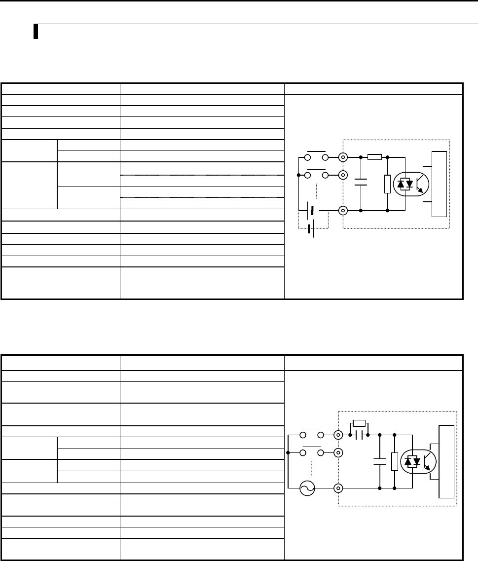
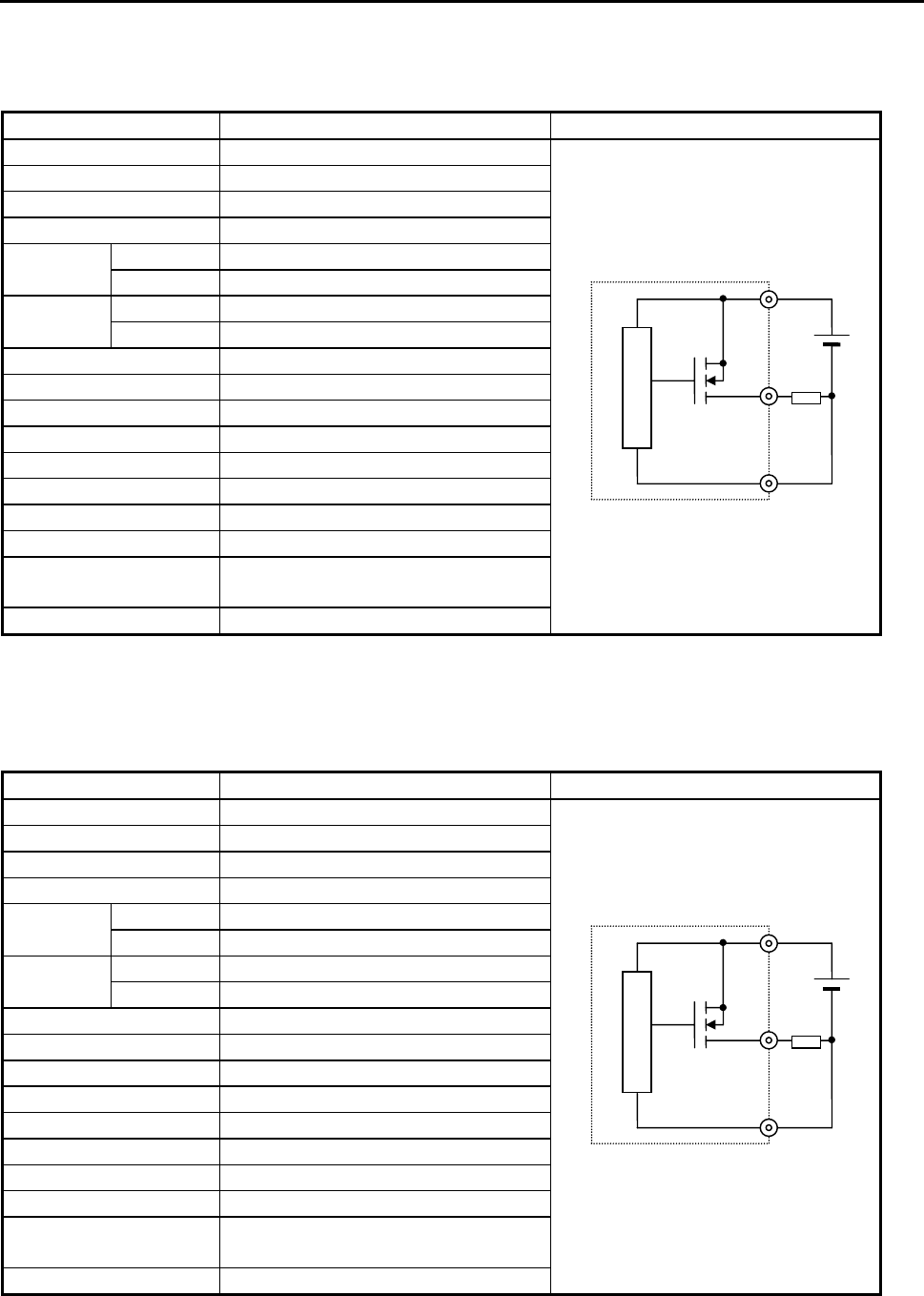
3.3.2 Input Specifications
The input circuit consists of DC input and AC input, with the following specifications.
(1) DC input
Item Specification Circuit diagram
Input voltage 24 V DC
Allowable input voltage range 0 to 30 V DC
Input impedance Approx. 2.8 kΩ
Input current 7.5 mA typical
ON voltage 15 V DC (min) / 4.5 mA (max)Operating
voltage OFF voltage 5 V DC (max) / 1.5 mA (max)
Basic unit : 0.5 to 20 ms (configurable)
OFF → ON Exp. unit : 0.5 ms or less
Basic unit : 0.5 to 20 ms (configurable)
Input lag
ON → OFF Exp. unit : 0.5 ms or less
Number of input points See Chapter 4
Number of common See Chapter 4
Polarity None
Insulation system Photocoupler insulation
Input display LED (green)
External connection 10-point type: fixed type terminal block
14-, 23-, 28-point types: Removable type
screw terminal block (M3)
*1: Common terminals are separated each other.
(2) AC input
Item Specification Circuit diagram
Input voltage 100 to 120 V AC
Allowable input voltage range 85 to 132 V AC
50 -5 % to 60 +5 % Hz
Input impedance Approx. 14.6 kΩ (60 Hz)
Approx. 17.6 kΩ (50 Hz)
Input current Approx. 7 mA RMS (100 V AC/60 Hz)
ON voltage 80 V AC (min.) 4.5 mAOperating
voltage OFF voltage 30 V AC (max.) 2 mA
OFF → ON 25 ms (max.) *1
Input lag
ON → OFF 30 ms (max.) *1
Number of input points See Chapter 4.
Number of common See Chapter 4.
Polarity None
Insulation system Photocoupler insulation
Input display LED (green)
External connection 14-, 28-point types: Removable type screw
terminal block (M3)
*1: Delay by hardware only. Delay by digital filter (software filter) 0.5 to 20 ms is not included.
*2: Common terminals are separated each other.
Internal circuit
0
1
C
Internal circuit
0
1
C
Chapter 3 Function and Performance Specifications
3-8
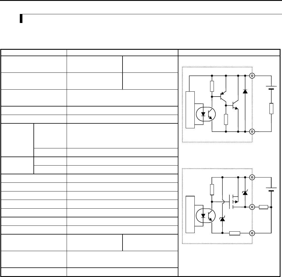
3.3.3 Output Specifications
(1) DC output
(Y100 of EH-*23DRP/A23DRT/*28DRP/*28DRT)
Item Specification Circuit diagram
Type EH-A23DRT
EH-*28DRT
EH-*23DRP
EH-*28DRP
Y100 output specifications Transistor output
(sink type)
Transistor output
(source type)
Rated load voltage 24 / 12 / 5 V DC
24 V DC +20 %, -80 %
Minimum switching current 1 mA
Leak current 0.1 mA (max)
1 circuit 0.75 A 24 V DC
0.5 A 12 V DC
0.25 A 5 V DC
Maximum
load current
1 common 0.75 A
OFF → ON 0.1 ms (max) 24 V DC 0.2 AOutput
response time ON → OFF 0.1 ms (max) 24 V DC 0.2 A
Number of output points 1
Number of common 1
Surge removing circuit None
Fuse None
Insulation system Photocoupler insulation
Output display LED (green)
External connection Removable type screw terminal block (M3)
External power supply *1
to V terminal
Not necessary 30 to 16 V DC
Insulation 1500 V or more (external-internal)
500 V or more (external-external)
Output voltage drop 0.3 V DC (max)
*1: It is necessary to supply 16 to 30 V DC between the V and C terminals externally for the source type.
The sink type operates by load power supply only. See “4.6 Terminal Layout and Wiring” for the details.
Sink type (23/28DRT)
Source type (23/28DRP)
0
C0
Internal circuit
V0
0
C0
Internal circuit
Chapter 3 Function and Performance Specifications
3-9
(2) DC output: LCDC-Low Current
(All points of EH-D10DT/DTP, Y102-Y105 of EH-D14DT/DTP, Y102-Y109 of EH-D28DT/DTP,
Y*018-Y*021 of EH-D14EDT/D14EDTP)
Item Specification Circuit diagram
Output specification Transistor output
Rated load voltage 24/12 V DC (+10 %, -15 %)
Minimum switching current 1 mA
Leak current 0.1 mA (max)
1 circuit 0.75 A 24 V DC
0.5 A 12 V DC
Maximum
load current
1 common 3 A
OFF → ON 0.1 ms (max) 24 V DC 0.2AOutput
response time ON → OFF 0.1 ms (max) 24 V DC 0.2A
Number of output points See Chapter 4.
Number of common See Chapter 4.
Surge removing circuit None
Fuse None
Insulation system Photocoupler insulation
Output display LED (green)
External connection Removable type screw terminal block (M3)
Externally supplied power *1 30 to 12 V DC
Insulation 1500 V or more (external-internal)
500 V or more (external-external)
Output voltage drop 0.3 V DC (max)
*1: It is necessary to supply 12 to 30 V DC between the V and C terminals externally. See “4.6 Terminal Layout and Wiring.”
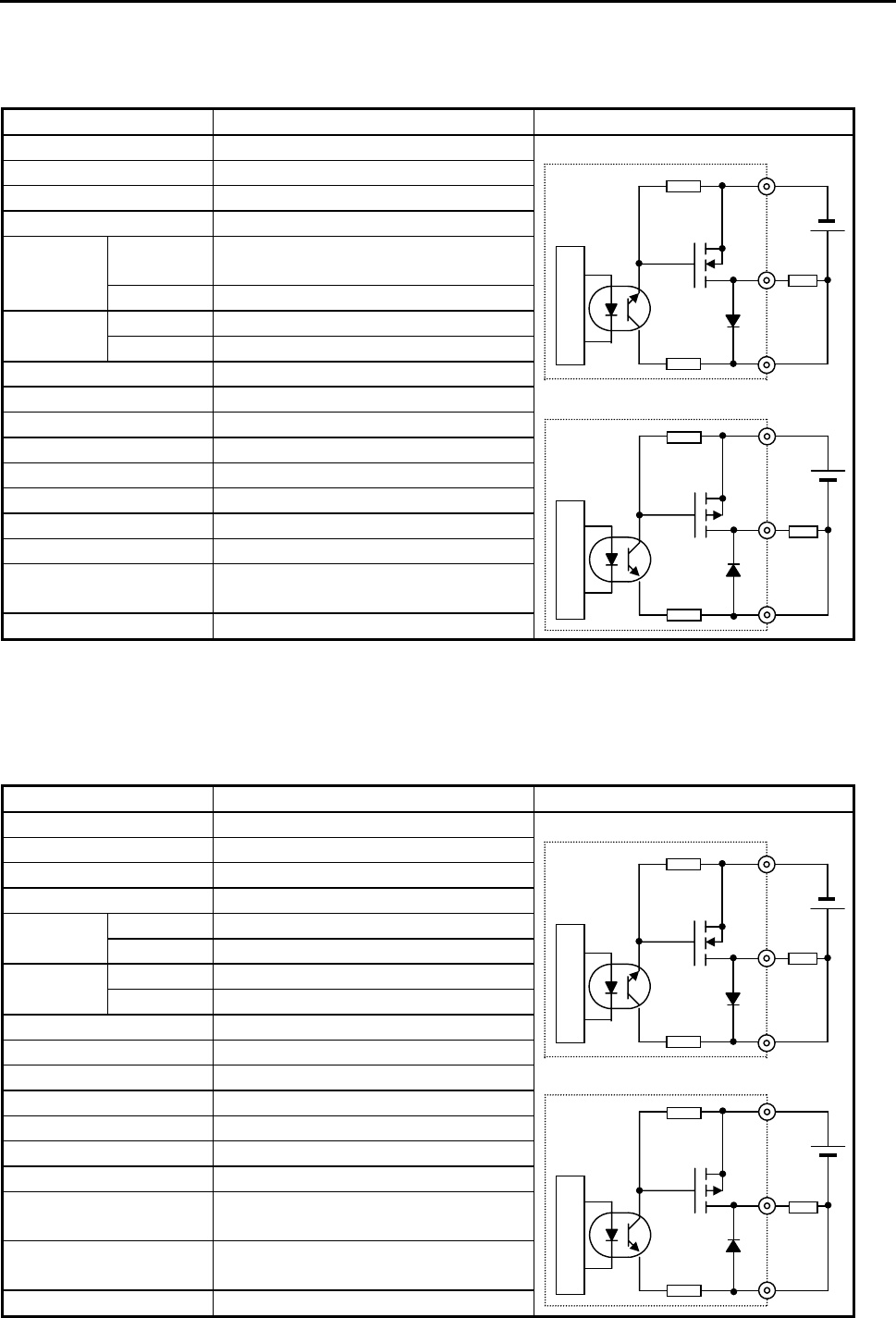
(3) DC output: HCDC-High Current
(Y100,Y101 of EH-D14DT/DTP, Y100, Y101, Y110, and Y111 of EH-D28DT/DTP,
Y*016, Y*017 of EH-D14EDT/D14EDTP)
Item Specification Circuit diagram
Output specification Transistor output
Rated load voltage 24/12 V DC (+10 %, -15 %)
Minimum switching current 1 mA
Leak current 0.1 mA (max)
1 circuit 1A 24 V DCMaximum
load current 1 common 3 A
OFF → ON 0.1 ms (max) 24 V DC 0.2AOutput
response time ON → OFF 0.1 ms (max) 24 V DC 0.2A
Number of output points See Chapter 4.
Number of common See Chapter 4.
Surge removing circuit None
Fuse None
Insulation system Photocoupler insulation
Output display LED (green)
External connection Removable type screw terminal block (M3)
Externally supplied power *1 30 to 12 V DC
Insulation 1500 V or more (external-internal)
500 V or more (external-external)
Output voltage drop 0.3 V DC (max)
*1: It is necessary to supply 12 to 30 V DC between the V and C terminals externally. See “4.6 Terminal Layout and Wiring.”
Internal circuit
V0
0
C0
Source type (EH-D**DTP)
Sink type (EH-D**DT)
V0
0
C0
Internal circuit Internal circuit
V0
0
C0
Source type (EH-D**DTP)
Sink type (EH-D**DT)
V0
0
C0
Internal circuit
Chapter 3 Function and Performance Specifications
3-10
(4) DC output (ESCP type): HCDC-High Current
(Y100,Y101 of EH-D14DTPS, Y100-Y103 of D28DTPS)
Y*016,Y*017 of EH-EDTPS, Y*016-Y*019 of EH-D28EDTPS)
Item Specification Circuit diagram
Output specification Transistor output
Rated load voltage 24/12 V DC (+10 %, -15 %)
Minimum switching current 10 mA
Leak current 0.1 mA (max)
1 circuit 1 AMaximum
load current 1 common 3 A
OFF → ON 0.05 ms (max) 24 V DC 0.2AOutput
response time ON → OFF 0.05 ms (max) 24 V DC 0.2A
Number of output points See Chapter 4.
Number of common See Chapter 4.
Surge removing circuit None
Fuse None
Insulation system Photocoupler insulation
Output display LED (green)
External connection Removable type screw terminal block (M3)
Externally supplied power *1 30 to 12 V DC
Insulation 1500 V or more (external-internal)
500 V or more (external-external)
Output voltage drop 0.3 V DC (max)
*1: It is necessary to supply 12 to 30 V DC between the V and C terminals externally. See “4.6 Terminal Layout and Wiring.”
(5) DC output (ESCP type): LCDC-Low Current
(Y102-Y105 of EH-D14DTPS, Y104-Y111 of EH-D28DTPS
Y*018-Y*021 of EH-D14EDTPS, Y*020-Y*027 of EH-D28EDTPS)
Item Specification Circuit diagram
Output specification Transistor output
Rated load voltage 24/12 V DC (+10 %, -15 %)
Minimum switching current 10 mA
Leak current 0.1 mA (max)
1 circuit 0.7 AMaximum
load current 1 common 3 A
OFF → ON 0.5 ms (max) 24 V DC 0.2AOutput
response time ON → OFF 0.5 ms (max) 24 V DC 0.2A
Number of output points See Chapter 4.
Number of common See Chapter 4.
Surge removing circuit None
Fuse None
Insulation system Photocoupler insulation
Output display LED (green)
External connection Removable type screw terminal block (M3)
Externally supplied power *1 30 to 12 V DC
Insulation 1500 V or more (external-internal)
500 V or more (external-external)
Output voltage drop 0.3 V DC (max)
*1: It is necessary to supply 12 to 30 V DC between the V and C terminals externally. See “4.6 Terminal Layout and Wiring.”
V0
0
C0
Source type (EH-D**DTPS)
Internal circuit
V0
0
C0
Source type (EH-D**DTPS)
Internal circuit
Chapter 3 Function and Performance Specifications
3-11
(6) Relay output
Item Specification Circuit diagram
Rated load voltage 5 to 250 V AC, 5 to 30 V DC
Minimum switching current 1 mA
1 circuit 2 A (24 V DC, 240 V AC)Maximum
load current 1 common 5 A
OFF → ON 15 ms (max)
Output
response time ON → OFF 15 ms (max)
Number of output points See Chapter 4.
Number of common See Chapter 4.
Surge removing circuit None
Fuse None
Insulation system Relay insulation
Output display LED (green)
External connection Removable type screw terminal block (M3)
Externally supplied power
(for driving the relays)
Not necessary
Contact life *1 20,000,000 times (mechanical)
200,000 times (electrical: 2 A)
Insulation 1500 V or more (external-internal)
500 V or more (external-external)
*1: Refer to the Life curve of relay contacts in Chapter 10 for the details.
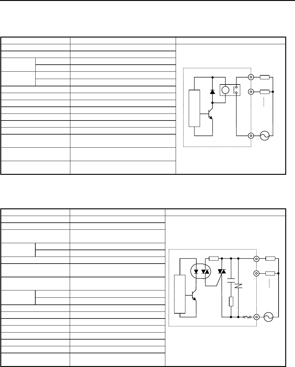
(7) AC output (SSR)
Item Specification Circuit diagram
Output specification Triac output
Rated voltage 100/240 V AC
Output voltage 100 –15 % to 240 +10 % V AC
50 –5 % to 60 +5 % Hz
1 circuit 0.5 A 240 V ACMaximum
load current 1 common 2 A
Minimum load current 100 mA
Maximum leakage current 1.8 mA 115 V AC(max)
3.5 mA 230 V AC(max)
Maximum inrush current 5 A (at 1 cycle or less)/point
10 A (at 1 cycle or less)/common
Off → On 1 ms or less
Maximum
delay time On → Off 1 ms + 1/2 cycle or less
Output common See Chapter 4.
Polarity See Chapter 4.
Insulation system Phototriac insulation
Fuse *2 Used
Surge removing circuit Sunabar circuit + varistor
External connection Removable terminal block
Voltage drop 1.5 V RMS (max)
Insulation 1500 V or more (external-internal)
500 V or more (external-external)
*2: It is necessary to repair the module if the load short-circuits and causes the fuse to melt.
Note that the fuse cannot be replaced by users.
0
1
C
Internal circuit
0
1
C
Internal circuit

Chapter 3 Function and Performance Specifications
3-12
3.3.4 High-Speed Counter Specifications
Single phase Two phase
Available input X0, X2, X4, X6 X0 and X2 in pair
Input voltage ON 15 V
OFF 5 V
Count pulse width 100 µs
Maximum count frequency 10 kHz each channel
Count register 16 bits
Coincidence output Allowed
On/Off-preset Allowed
Upper/lower limit setting Not allowed
Preload/strobe Allowed
Since 10 points type does not have input X6, counter channel is up to 3 ch.
3.3.5 PWM Output/Pulse Train Output Specifications
23-point and 28-point type
Relay Output
10/14/28-point
Transistor Output
Available outputs Y100 (optional) Y100-Y103 (optional)
Load voltage 5/12/24 V 12/24 V
Minimum load current 1 mA
PWM max. output frequency *1 2 kHz total channels
Pulse train max. output frequency *1 5 kHz total channels
Pulse acceleration/deceleration By FUN 151.
*1: Relay outputs cannot keep up with high frequencies; these outputs should be used at the operating frequency upon confirmation.
3.3.6 Analogue Input Specifications
Module type 23 points module Analog exp. unit
Input channel WX30, WX31 WX u01 - WX u04
(u : unit number)
0-10 V (10.24V max.) 0-10V (10.24V max.)
-10 to +10V (±10.24V max.)
0-20 mA (20.48 mA max.) 0-20 mA (20.48 mA max.)
Input range
- 4-20 mA (20.38 mA max.)
Resolution 12 bits
Accuracy ±1 % of full scale
Linearity Max. +/-3 units
Current input impedance Approx. 249 Ω
Voltage input impedance Approx. 100 kΩApprox. 200 kΩ
Input delay time 20 ms
Channel to internal circuit insulation Not insulated Insulated
Channel-to-channel insulation Not insulated
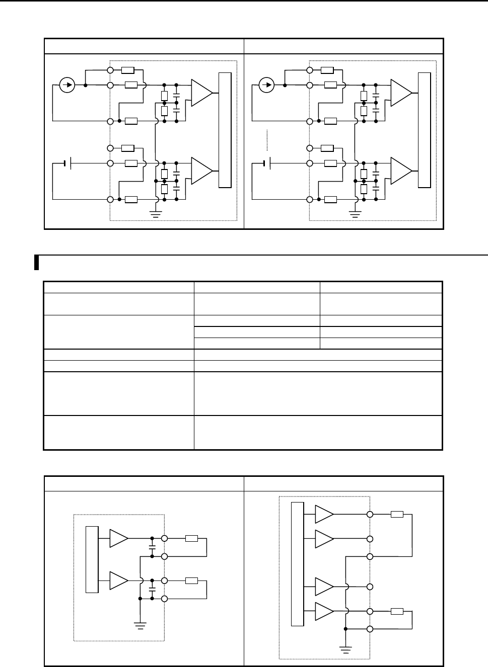
Chapter 3 Function and Performance Specifications
3-13
Circuit diagram (23 points type) Circuit diagram (Analog expansion unit)
3.3.7 Analogue Output Specifications
Module type 23 points type module Analog exp. unit
Output channel WY40 WY u06, WY u07
(u : unit number)
0-10V (10.24V max.) 0-10V (10.24V max.)
0-20mA (20.48mA max.) 0-20mA (20.48mA max.)
Output range
4-20mA (20.38mA max.)
Resolution 12 bits
Accuracy ±1 % of full scale
Current output
Allowable load
Output allowable capacity
Output allowable inductance
10 to 500 Ω
Maximum 2000 pF
Maximum 1 H
Voltage output
Allowable load
Output allowable impedance
Maximum 10 kΩ
Maximum 1 µF
Circuit diagram (23 points type) Circuit diagram (Analog expansion unit)
VO7
IO7
OC7
VO6
IO6
OC6
Voltage
Current
Internal circuit
Voltage
Current
IN2JP
IN2+
IN2-
IN1JP
IN1+
IN1-
Internal circuit
Current
Voltage
IN4JP
IN4+
IN4-
IN1JP
IN1+
IN1-
Internal circuit
VO
VC
IO
IC
Internal circuit
Voltage
Current
Chapter 3 Function and Performance Specifications
3-14
3.3.8 Potentiometer Analogue Input Specifications
Number of potentiometer inputs 2
Stored in Ch.1 : WRF03E, Ch.2 WRF03F
Input range 0-1023 (H0-H3FF)
Resolution 10 bits
Input filter By user settings
3.3.9 Interrupt Input Specifications
Input that can be used X1, X3, X5, X7 (by user settings)
ON 15 VInput voltage
OFF 5 V
3.3.10 Backup
(1) Battery
Data memory (retentive area) can be kept by EH-MBAT battery as below.
Battery life time (total power off time) [Hr] *
Guaranteed value (Min.) @55°C Actual value (Max.) @25°C
9,000 18,000
* Battery life time has been changed since Oct. 2002 production (MFG NO.02Jxx) due to hardware modification.
Battery can be mounted inside of front cover.
Battery is available only for 23-point and 28-point types.
If the calendar clock function is used with the 23-point or 28-point type, be sure to use the battery.
(2) Capacitor
14-point type: Data can be kept for 72 hours (at 25 °C) by the capacitor.
23 and 28-point types: Data can be kept for 24 hours (at 25 °C) by the capacitor.
Please note that data memory of 10 point type cannot be retained.
3.3.11 Expansion
•Up to 4 times of expansion units can be installed.
•14 points and 28 points digital units, and 4ch. input / 2 ch. output analog expansion units available.
•A cable with a length of up to 1 m can be used to connect between units.
•The total extension cable length can be up to 2 m (from the basic unit to the expansion unit at the end).
•The 10-point type unit cannot be expanded.

Chapter 3 Function and Performance Specifications
3-15
3.3.12 Clock Function
23-point and 28-point types have calendar function. This can be operated either by internal output area or task code.
* 10-point and 14-point types do not have this function.
(1) Reading the clock data
By turning on the read request (R7F8), the clock data is read out in the reading value area (WRF01B to WRF01F).
(2) Writing the clock data
By turning on the write request (R7F9), the clock data stored in writing value area (WRF01B to WRF01F) is written
to the current data area (WRF00B to WRF00F). If the data is wrong, error flag (R7BF) will turn on. If data is right,
clock data will be written and writing flag R7FB will turn off.
(3) Adjusting the clock data ± 30 seconds
By turning on the ± 30 seconds adjustment request (R7FA), one of the following operations is performed depending
on the second value:
•If the second digits are 00 to 29, the second digits are set to 00.
•If the second digits are 30 to 59, the minute is incremented by 1 and the second digits are set to 00.
(4) Special internal output definitions
•Operation bits
I/O number Name Description
R7F8 Request to read calendar and
clock data
Calendar and clock data is read out to
WRF01B-F01F.
R7F9 Request to write calendar and
clock data
Calendar and clock data in WRF01B-F01F is
written to the current data in WRF00B-F00F.
R7FA Clock ± 30 seconds adjustment
request
Sets the second digits of the RTC to 00.
R7FB Calendar and clock setting data
error
Turns on when the setting data is abnormal.
•Current data monitor area : Current data of the clock given always (all BCD data).
I/O number Name Description
WRF00B Year 4-digit year [yyyy]
WRF00C Month and date [mmdd]
WRF00D Day of the week 0 to 6 : Sunday to Saturday
WRF00E Hour and minute [hhmm] (24-hour system).
WRF00F Second [00ss]
•Reading/writing area : Clock data to be read or written.
(All BCD data)
I/O number Name Description
WRF01B Year 4-digit year [yyyy]
WRF01C Month and date [mmdd]
WRF01D Day of the week 0 to 6 : Sunday to Saturday
WRF01E Hour and minute [hhmm] (24-hour system).
WRF01F Second [00ss]
Note 1: The day of the week data is expressed as follows.
0: Sunday, 1: Monday, 2: Tuesday, 3: Wednesday, 4: Thursday, 5: Friday, 6: Saturday

Chapter 3 Function and Performance Specifications
3-16
3.3.13 Power Supply for Sensor
The 24 V terminal at the input terminal part can supply current to external equipment (not for all units).
If this terminal is used as the power supply for the input part of this unit, the remaining can be used as power supply for the
sensors.
The following current (I) can be supplied as power supply for the sensors.
(1) EH-*14*** (14-point type basic unit)
EH-*14E*** (14-point type extension unit)
I = 350 mA – (7.5 mA x number of input points that are turned on at the same time)
(2) EH-A28DR* (28-point type basic unit)
EH-A23DR*** (23-point type basic unit)
I = 280 mA – (7.5 mA x number of input points that are turned on at the same time)

Chapter 4 Product lineup and wiring
4-1
Chapter 4 Product lineup and wiring
4.1 Product lineup
(1) Basic units
Table 4.1 Product lineup list
Type Specifications I/O assignment
symbol
EH-D10DT DC power, DC input × 6, Transistor (sink) output × 4 X48/Y32/empty16
EH-D10DTP DC power, DC input × 6, Transistor (source) output × 4 X48/Y32/empty16
EH-D10DR DC power, DC input × 6, Relay output × 4 X48/Y32/empty16
EH-D14DT DC power, DC input × 8, Transistor (sink) output × 6 X48/Y32/empty16
EH-D14DTP DC power, DC input × 8, Transistor (source) output × 6 X48/Y32/empty16
EH-A14DR AC power, DC input × 8, Relay output × 6 X48/Y32/empty16
EH-D14DR DC power, DC input × 8, Relay output × 6 X48/Y32/empty16
EH-A14AS AC power, AC input × 8, SSR output × 6 X48/Y32/empty16
EH-D23DRP DC power, DC input × 13, Relay output × 9, Transistor output (source) × 1,
Analog input × 2, Analog output × 1
X48/Y32/
empty16/WX4/WY4
EH-A23DRT AC power, DC input × 13, Relay output × 9, Transistor output (sink) × 1,
Analog input × 2, Analog output × 1
X48/Y32/
empty16/WX4/WY4
EH-A23DRP AC power, DC input × 13, Relay output × 9, Transistor output (source) × 1,
Analog input × 2, Analog output × 1
X48/Y32/
empty16/WX4/WY4
EH-D28DT DC power, DC input × 16, Transistor (sink) output × 12 X48/Y32/empty16
EH-D28DTP DC power, DC input × 16, Transistor (source) output × 12 X48/Y32/empty16
EH-D28DTPS DC power, DC input × 16, Transistor (source) output (ESCP) × 12 X48/Y32/empty16
EH-D28DRT DC power, DC input × 16, Relay output × 11, Transistor output (sink) × 1 X48/Y32/empty16
EH-D28DRP DC power, DC input × 16, Relay output × 11, Transistor output (source) × 1 X48/Y32/empty16
EH-A28DRT AC power, DC input × 16, Relay output × 11, Transistor output (sink) × 1 X48/Y32/empty16
EH-A28DRP AC power, DC input × 16, Relay output × 11, Transistor output (source) × 1 X48/Y32/empty16
EH-A28DR AC power, DC input × 16, Relay output × 12 X48/Y32/empty16
EH-A28AS AC power, AC input × 16, SSR output × 12 X48/Y32/empty16
EH-D14EDT Expansion unit, DC power, DC input × 8, Transistor (sink) output × 6 B1/1
EH-D14EDTP Expansion unit, DC power, DC input × 8, Transistor (source) output × 6 B1/1
EH-D14EDTPS Expansion unit, DC power, DC input × 8, Transistor (source) output (ESCP) × 6 B1/1
EH-D14EDR Expansion unit, DC power, DC input × 8, Relay output × 6 B1/1
EH-A14EDR Expansion unit, AC power, DC input × 8, Relay output × 6 B1/1
EH-D28EDT Expansion unit, DC power, DC input × 16, Transistor (sink) output × 12 B1/1
EH-D28EDTPS Expansion unit, DC power, DC input × 16, Transistor (source) output (ESCP) × 12 B1/1
EH-D28EDR Expansion unit, DC power, DC input × 16, Relay output × 12 B1/1
EH-A28EDR Expansion unit, AC power, DC input × 16, Relay output × 12 B1/1
EH-D6EAN Expansion unit, DC power, Analog input × 4, Analog output × 2 FUN 0
EH-A6EAN Expansion unit, AC power, Analog input × 4, Analog output × 2 FUN 0
Each digit in the type name has the following meaning:
EH - D 28 D T P
[None]: Sink, T: Sink, P: Source (except in the cases of relay output and SSR output)
R: Relay output, T: Transistor (DC) output, S: SSR (AC) output
D: DC input, A: AC input
[None]: Basic unit, E: Expansion unit
10: 10-point type, 14: 14-point type, 23: 23-point type, 28: 28-point type
A: AC power supply type, D: DC power supply type
Chapter 4 Product lineup and wiring
4-2
(2) Peripheral Units
Table 4.2 List of peripheral units
Product Form Specification Remarks
HL-GPCL Ladder diagram/Instruction language editor LADDER EDITOR (for GPCL)
HL-PC3 Ladder diagram/Instruction language editor LADDER EDITOR (for PC98
series) with CPU connection cable
HL-AT3E Ladder diagram/Instruction language editor LADDER EDITOR (for PC/AT
compatible personal computer)
Graphic input
device support
software
HLW-PC3 Ladder diagram/Instruction language editor LADDER EDITOR (for Windows®
95/NT 4.0)
HLW-PC3E Ladder diagram/Instruction language editor LADDER EDITOR (for Windows®
95/98/NT 4.0)
Pro-H HITACHI H-series PLC Programming Software According to IEC 61131-3 (for
Windows® 95/98/NT 4.0)
Note: HI-LADDER (attached to the GPCL01H) may also be used.
However, HL-GPCL and HI-LADDER cannot be used for the 10-point type.
(3) Connection Cables
Table 4.3 List of connection cables
Product Form Specification Remarks
EH-MCB10 Length: 1 m (basic unit–exp. unit, exp. unit - exp. unit) Total 2 mCable for connecting basic unit
and expansion unit EH-MCB05 Length: 0.5 m (basic unit–exp. unit, exp. unit - exp. unit) Total 2 m
EH-MCB01 Length: 0.1 m (basic unit–exp. unit, exp. unit - exp. unit) Total 2 m
Conversion cable for
connecting peripheral units
EH-RS05 Length: 0.5 m *
Peripheral equipment GPCB02H Length: 2 m, between CPU and graphic input unit
GPCB05H Length: 5 m, between CPU and graphic input unit
GPCB15H Length: 15 m, between CPU and graphic input unit
CBPGB Length: 2 m, between graphic input unit and printer
LP100 Length: 2 m, between graphic input unit and kanji printer
KBADPTH Length: 15 m, between graphic input unit and JIS keyboard
PCCB02H Length: 2 m, between CPU and PC98 series **
WPCB02H Length: 2 m, between CPU and PC98 series (25-pin) **
WVCB02H Length: 2 m, between CPU and DOS/V (9-pin) **
EH-VCB02 Length: 2 m, between CPU (8P modular terminal) and DOS/V
(9-pin)
*: Required when connecting the MICRO-EH with PC98, IBM PC/AT compatible PC or other system using one of the cables
marked with **.
(4) Others
Model Usage Remarks
EH-MBAT Lithium battery
Chapter 4 Product lineup and wiring
4-3
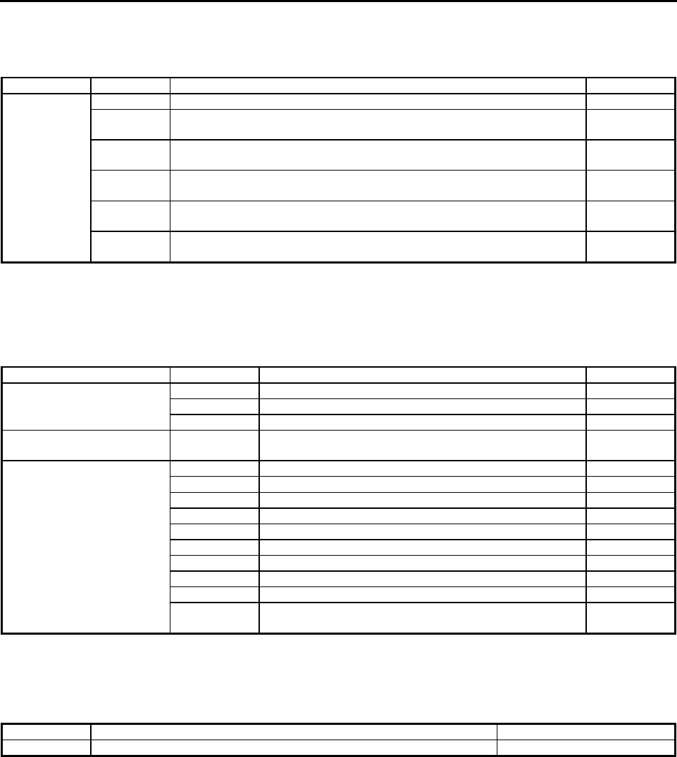
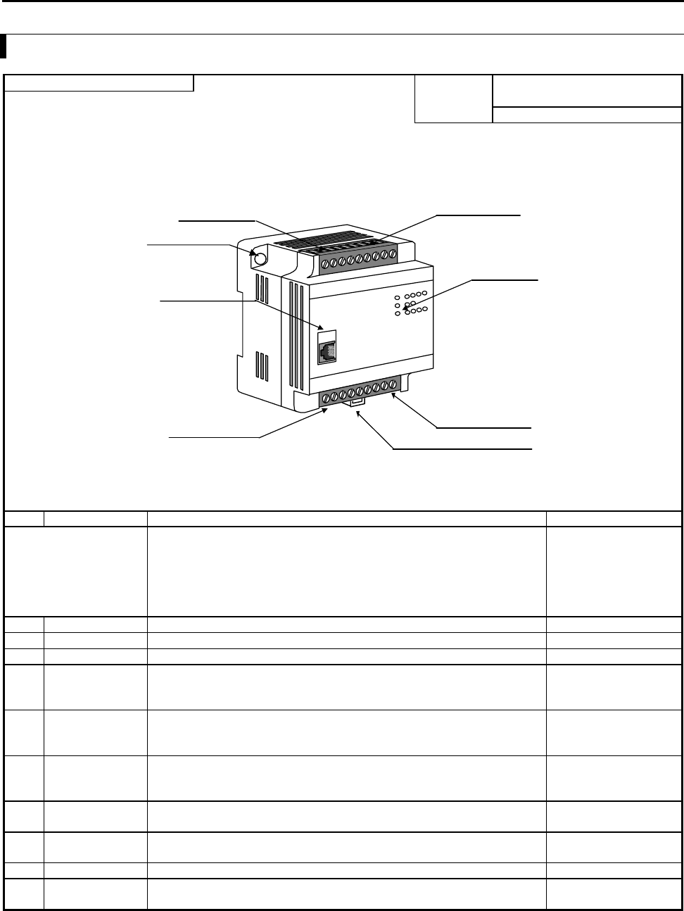
4.2 10-Point Basic Unit
Name and function of each part Type EH-D10DT, EH-D10DTP, EH-
D10DR
1] POW LED
2] OK LED
3] RUN LED
4] Serial port
5] RUN input
9] Mounting hole
8] Power terminal
7] Output terminals
10] DIN rail installation clip
6] Input terminals
No. Item Detailed explanation Remarks
Explanation of operation Operations are performed according to the contents of the program created
by the user.
The programming unit connected to the CPU module communication port
writes and reads the user programs.
Memory is installed inside the CPU module in which the user programs and
internal output information are stored.
1] POW LED Lighting when the power is supplied.
2] OK LED Lighting at normal operation. See Chapter 12.
3] RUN LED Lighting at RUN status.
4] Serial port 1 Serial port for connecting the peripheral units. Communication speed is
fixed as 4800 bps.
The communication specification is set to port 1.
See Chapter 11.
5] RUN input External input to control the PLC’s RUN/STOP.
When 24 V DC is loaded to the RUN terminal and common terminal (C),
the PLC is set to the RUN state.
See Chapter 10.
6] Input terminals Terminals for wiring the external input units.
One piece of AWG14 to AWG22 (2.1 to 0.36 mm2) or two pieces of
AWG16 to AWG22 (1.3 to 0.36 mm2) per terminal may be wired.
See Chapter 10.
7] Output terminals Terminals for connecting the external load. The wiring specification is the
same as for the input terminals.
See Chapter 10.
8] Power terminal Terminal for connecting the power supply. The wiring specification is the
same as for the input terminals.
See Chapter 10.
9] Mounting hole Used when installing the PLC directly on a board with screws See Chapter 10.
10] DIN rail
installation clip
Used when installing the PLC on a DIN rail See Chapter 10.
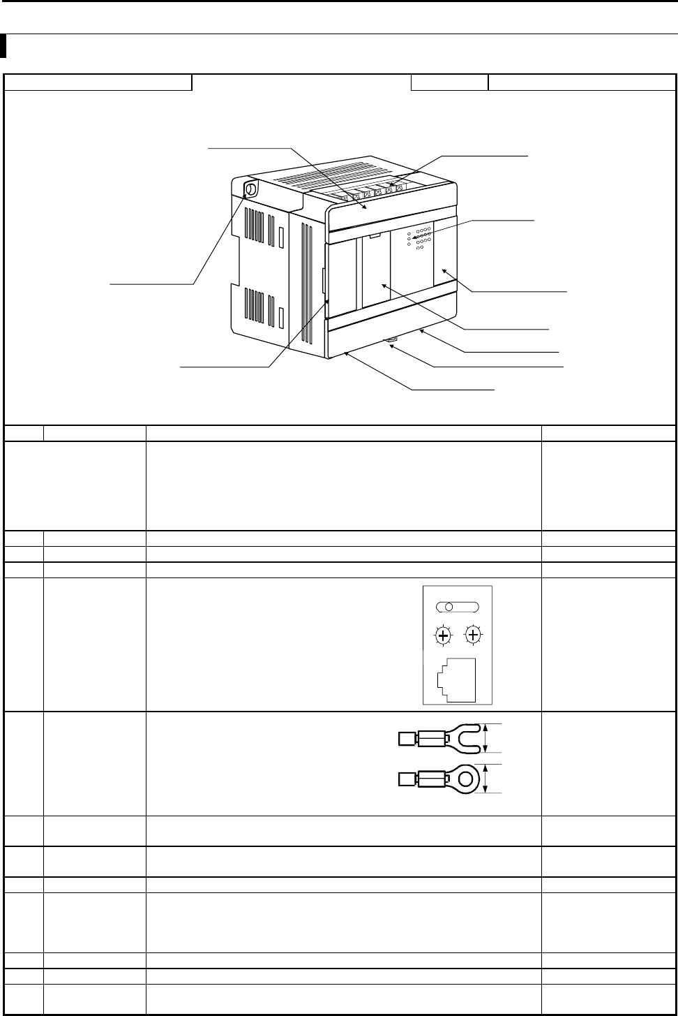
Chapter 4 Product lineup and wiring
4-4
4.3 14-Point Basic Unit
Name and function of each part Type EH-*14***
1] POW LED
2] OK LED
3] RUN LED
10] Terminal cover
4] Serial port cover
11] Mounting hole
5] Input terminals
8] Expansion
connector cover
9] DIP SW cover
6] Output terminals
12] DIN rail installation clip
7] Power terminal
No. Item Detailed explanation Remarks
Explanation of operation Operations are performed according to the contents of the program created
by the user.
The programming unit connected to the CPU module communication port
writes and reads the user programs.
Memory is installed inside the CPU module in which the user programs and
internal output information are stored.
1] POW LED Lighting when the power is supplied.
2] OK LED Lighting at normal operation. See Chapter 12.
3] RUN LED Lighting at RUN status.
4] Serial port cover Cover for the connector for connecting
peripheral units and the RUN switch.
When the cover is opened, the RUN switch,
potentiometers (VR), and RS-232C serial port 1
(PORT 1) can be used.
The communication specification is set to port 1.
See Chapters 8 and 11.
5] Input terminals Terminals for wiring the external input units.
Recommended terminals are shown in the
figure to the right.
One piece of AWG14 to AWG22 (2.1 to
0.36 mm2) or two pieces of AWG16 to
AWG22 (1.3 to 0.36 mm2) per terminal may
be wired.
See Chapter 10.
(Make sure that the terminals will not
disengage due to loose screws.)
(Recommended)
6] Output terminals Terminals for connecting the external load.
The wiring specification is the same as for the input terminals.
See Chapter 10.
7] Power terminal Terminal for connecting the power supply.
The wiring specification is the same as for the input terminals.
See Chapter 10.
8] Expansion cover Cover for the expansion connector See Chapter 10.
9] DIP SW cover Cover for the DIP switches
When the cover is opened, the DIP switches are exposed. These DIP
switches are used to set the communication speed of serial port 1 and the
modem connection.
See Chapter 11.
10] Terminal cover Cover for terminals
11] Mounting hole Used when installing the PLC with screws See Chapter 10.
12] DIN rail
installation clip
Used when installing the PLC on a DIN rail See Chapter 10.
STOP RUN
VR1 VR2
PORT1
6
6
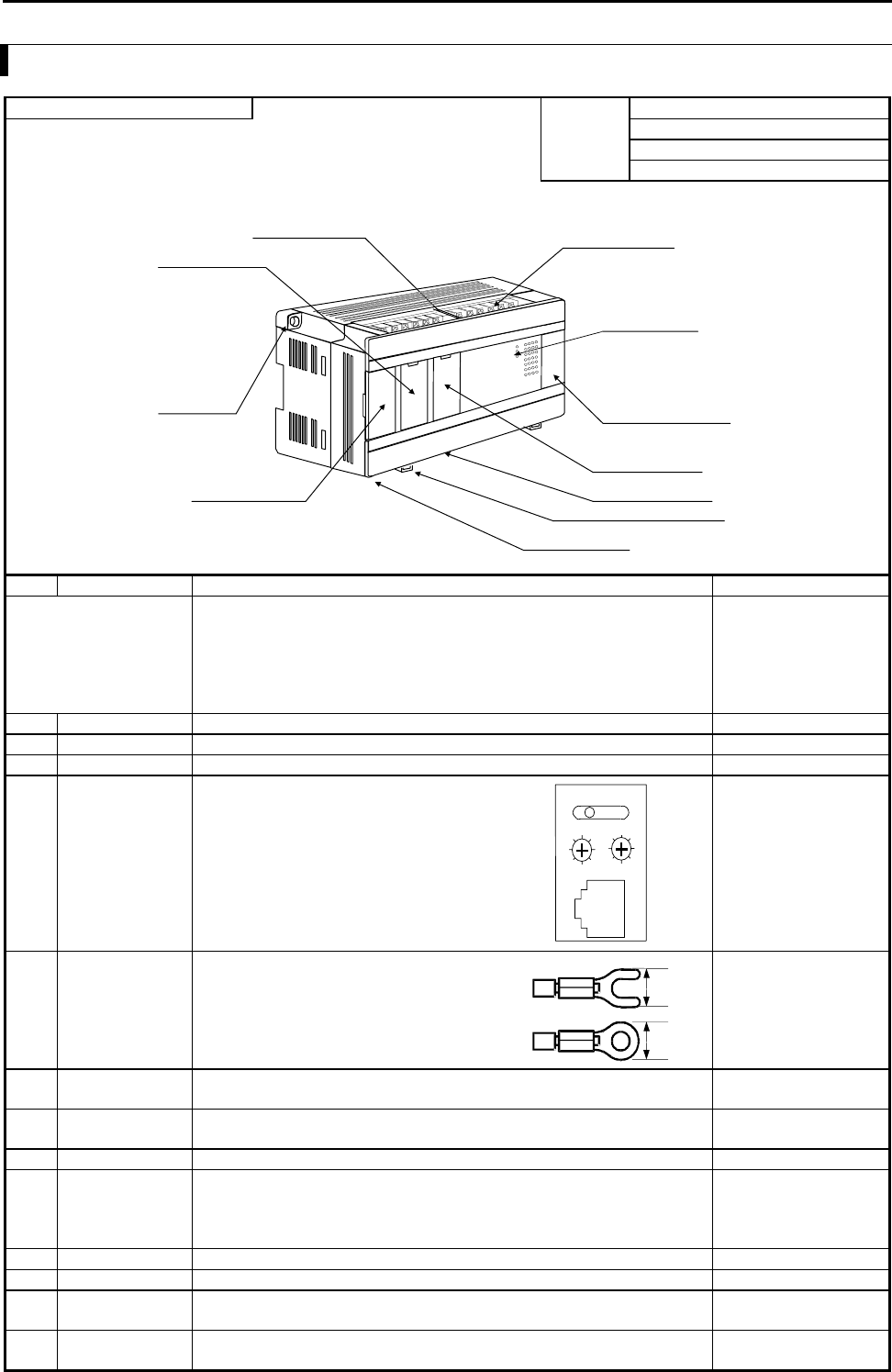
Chapter 4 Product lineup and wiring
4-5
4.4 23-Point and 28-Point Basic Unit
Name and function of each part EH-*23***
EH-*28***
Type
1] POW LED
2] OK LED
3] RUN LED
10] Terminal cover
13] RS-485 port cover
11] Mounting
hole
4] Serial port cover
5] Input terminals
8] Expansion
connector cover
9] DIP SW cover
6] Output terminals
12] DIN rail installation clip
7] Power terminal
No. Item Detailed explanation Remarks
Explanation of operation Operations are performed according to the contents of the program created
by the user.
The programming unit connected to the CPU module communication port
writes and reads the user programs.
Memory is installed inside the CPU module in which the user programs and
internal output information are stored.
1] POW LED Lighting when the power is supplied.
2] OK LED Lighting at normal operation. See Chapter 12.
3] RUN LED Lighting at RUN status.
4] Serial port cover Cover for the connector for connecting
peripheral units and the RUN switch.
When the cover is opened, the RUN switch,
potentiometers (VR), and RS-232C serial port 1
(PORT 1) can be used.
The communication specification is set to port 1.
See Chapters 8 and 11.
5] Input terminals Terminals for wiring the external input units.
Recommended terminals are shown in the figure
to the right.
One piece of AWG14 to AWG22 (2.1 to 0.36
mm2) or two pieces of AWG16 to AWG22 (1.3
to 0.36 mm2) per terminal may be wired.
See Chapter 10.
(Make sure that the terminals will not
disengage due to loose screws.)
(Recommended)
6] Output terminals Terminals for connecting the external load.
The wiring specification is the same as for the input terminals.
See Chapter 10.
7] Power terminal Terminal for connecting the power supply.
The wiring specification is the same as for the input terminals.
See Chapter 10.
8] Expansion cover Cover for the expansion connector See Chapter 10.
9] DIP SW cover Cover for the DIP switches and the backup battery storage unit.
When the cover is opened, the DIP switches are exposed. These DIP
switches are used to set the communication speed of serial port 1 and the
modem connection.
See Chapter 11.
10] Terminal cover Cover for terminals
11] Mounting hole Used when installing the PLC with screws See Chapter 10.
12] DIN rail
installation clip
Used when installing the PLC on a DIN rail See Chapter 10.
13] RS-485 port cover Cover for RS-485 port. It is connected with a D sub 15-pin female
connector. The communication specification is set to port 2.
See Chapter 11.
STOP RUN
VR1 VR2
PORT1
6
6
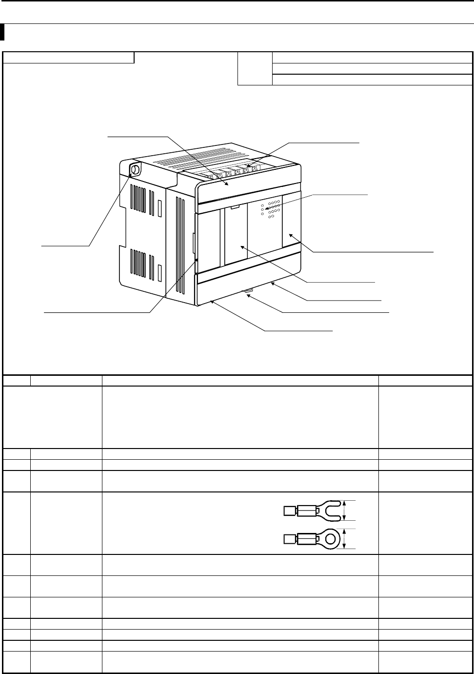
Chapter 4 Product lineup and wiring
4-6
4.5 Expansion Unit
Name and function of each part Type EH-*14ED** (same dimension as 14 pts. basic unit)
EH-*28ED** (same dimension as 28 pts. basic unit)
EH-*6EAN (same dimension as 14 pts. basic unit)
1] POW LED
2] OK LED
3] Expansion connector cover
(left side)
9] Terminal cover
10] Mounting
hole
4] Input terminals
7] Expansion connector cover
(right side)
8] Dummy cover
5] Output terminals
11] DIN rail installation clip
6] Power terminal
Above picture is 14 points module
No. Item Detailed explanation Remarks
Explanation of operation Operations are performed according to the contents of the program created
by the user.
The programming unit connected to the CPU module communication port
writes and reads the user program.
Memory is installed inside the CPU module in which the user program and
internal output information are stored.
1] POW LED Lighting when the power is supplied.
2] OK LED Lighting at normal operation.
3] Expansion cover
(Left side)
Cover for expansion connector
Used when connecting to the expansion cable from the front unit.
See Chapter 10.
4] Input terminals Terminals for wiring the external input units.
Recommended terminals are shown in the figure
to the right.
One piece of AWG14 to AWG22 (2.1 to 0.36
mm2) or two pieces of AWG16 to AWG22 (1.3
to 0.36 mm2) per terminal may be wired.
See Chapter 10.
(Make sure that the terminals will not
disengage due to loose screws.)
(Recommended)
5] Output terminals Terminals for connecting the external load. The wiring specification is the
same as for the input terminals.
See Chapter 10.
6] Power terminal Terminal for connecting the power supply. The wiring specification is the
same as for the input terminals.
See Chapter 10.
7] Expansion cover
(Right side)
Cover for expansion connector
Used when connecting to the next unit.
See Chapter 10.
8] Dummy cover Cover used as a dummy.
9] Terminal cover Cover for terminals
10] Mounting hole Used when installing the PLC with screws See Chapter 10.
11] DIN rail
installation clip
Used when installing the PLC on a DIN rail See Chapter 10.
6
6
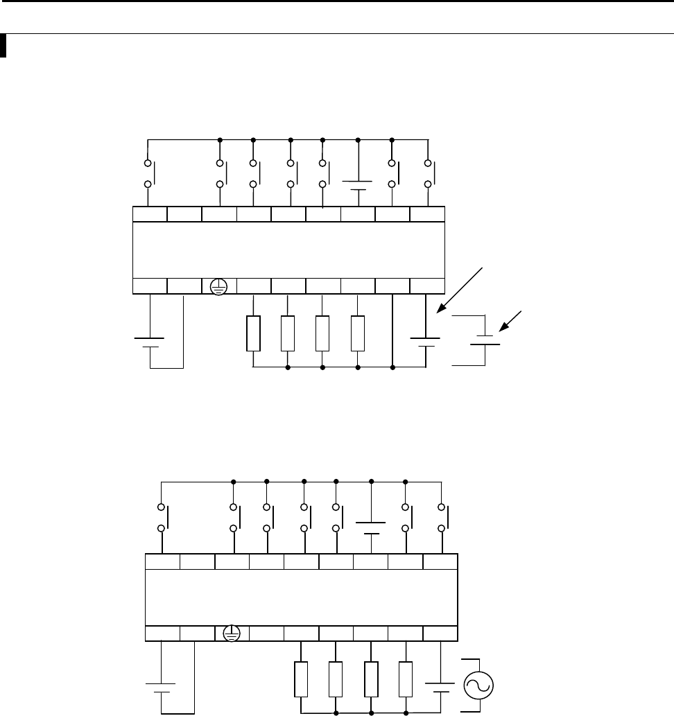
Chapter 4 Product lineup and wiring
4-7
4.6 Terminal Layout and Wiring
10-point type
EH-D10DT, EH-D10DTP
* Since the DC input is bidirectional, it is possible to reverse the polarity of the power supply.
EH-D10DR
* Since the DC input is bidirectional, it is possible to reverse the polarity of the power supply.
54C032RUN 10NC
V0C032124 V 00 V
Load power supply
12/24V DC
Power supply
24V DC
Input power supply
24 V DC
Power supply
24V DC
Load power supply
24V DC
100-240V AC
Input power supply
24V DC
In case of EH-D10DTP
In case of EH-D10DT
54C032RUN 10NC
C0321024V NC0V
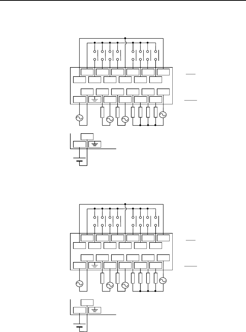
Chapter 4 Product lineup and wiring
4-8
14-point type
EH-A14DR, EH-D14DR
* Since the DC input is bidirectional, it is possible to reverse the polarity of the power supply.
EH-A14EDR, EH-D14EDR
* Since the DC input is bidirectional, it is possible to reverse the polarity of the power supply.
AC power supply
100-240V AC
Input power supply
24V DC
DC power supply
24V DC
Load power supply
24V DC,
100-240V AC
0
24+
0V 2
1
C0
3
5
4
7
6C1
AC
AC C0
0
C1
1
3
2
5
4C2
Input
Output
0V
24V
AC power supply
100-240V AC
Input power supply
24V DC
DC power supply
24V DC
Load power supply
24V DC,
100-240V AC
0
24+
0V 2
1
C0
3
5
4
7
6C1
AC
AC C0
16
C1
17
19
18
21
20 C2
Input
Output
0V
24V
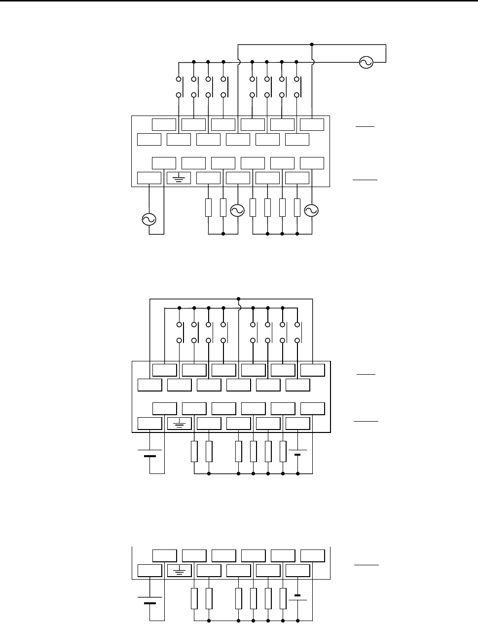
Chapter 4 Product lineup and wiring
4-9
EH-A14AS
EH-D14DTP
* Since the DC input is bidirectional, it is possible to reverse the polarity of the power supply.
EH-D14DT
(The input wiring is the same as EH-D14DTP.)
Load power supply
100-240V AC
Power supply for input
100-115V AC
Power supply
100-240V AC
0
24+
0V 2
1
C0
3
5
4
7
6C1
AC
AC 0
NC
C0
1
3
2
5
4C1
Input
Output
Load power supply
12/24V DC
Power supply for input
24V DC
Power supply
24V DC
00V 2
1
C0
3
5
4
7
6C1
0V
24V 1
0
2
NC
4
3
V0
5C0
24+ Input
Output
Load power supply
12/24V DC
Power supply
24V DC
0V
24V 1
0
2
NC
4
3
V0
5C0 Output
Chapter 4 Product lineup and wiring
4-10
EH-D14EDTP
* Since the DC input is bidirectional, it is possible to reverse the polarity of the power supply.
EH-D14EDT
(The input wiring is the same as EH-D14EDTP.)
Load power supply
12/24V DC
Power supply
24V DC
0V
24V 17
16
18
NC
20
19
V0
21 C0
Load power supply
12/24V DC
Power supply
24V DC
0
24+
0V 2
1
C0
3
5
4
7
6C1
0V
24V 17
16
18
NC
20
19
V0
21 C0
Input
Output
Output
Chapter 4 Product lineup and wiring
4-11
23-point type
EH-A23DRP
* Since the DC input is bidirectional, it is possible to reverse the polarity of the power supply.
EH-A23DRT EH-D23DRP
(The input wiring is the same as EH-A23DRP.)
TR output power supply
16-30V DC
Power supply
100-240V AC
Power supply for
input, 24V DC
Load power supply
24V DC,
100-240V AC
Power supply
100-240V AC
In case of analog current input, please set
the following value in WRF06E.
WRF06E ch-0 ch-1
H0000 Voltage Voltage
H4000 Voltage Current
H8000 Current Voltage
HC000 Current Current
Please refer to Chapter 8-9.
+
-
0
24+
0V 2
1
C0
3
5
4
7
6C1
AC
AC C0
0
1
V0
3
2
C1
4 5
C3
6
C2 C4
7
9
8
IC VC
IO VO
9
8
C2 11
10
IN1-
12
IN1JP
IN1+
IN2+
IN2- IN2JP
C5
Input
Output
AC
AC C0
0
1
NC 2Output 0V
24V
0
1
V0 2Output
C0
TR output power supply
16-30V DC
TR output power supply
16-30V DC
Analog output
Analog voltage input
IN1- IN1JP
IN1+
IN2+
IN2- IN2JP
Analog current input
IN1- IN1JP
IN1+
IN2+
IN2- IN2JP
Chapter 4 Product lineup and wiring
4-12
28-point type
EH-A28DRP
* Since the DC input is bidirectional, it is possible to reverse the polarity of the power supply.
EH-A28DRT
(The input wiring is the same as EH-A28DRP.)
EH-D28DRP
(The input wiring is the same as EH-A28DRP.)
EH-D28DRT
(The input wiring is the same as EH-A28DRP.)
TR output power supply
16-30V DC
Load power supply
24V DC, 100-240V AC
Power supply
100-240V AC
Power supply
for input 24V DC
TR output power supply
16-30V DC
Power supply
24V DC
Power supply
100-240V AC
0
24+
0V 2
1
C0
3
5
4
7
6C1
AC 0
1
V0
3
2
C1
4 5
C3
6
C2 C4
7
C5
8
10 C6
11 C6
10
9
8C2
11
12
C2
14
13
C3
15 C3
9
AC C0
Input
Output
AC
AC C0
0
1
NC 2
Output
0V
24V C0
0
1
V0 2
0V
24V C0
0
1
NC 2
Output
Power supply
24V DC
Output
Chapter 4 Product lineup and wiring
4-13
EH-A28AS
EH-D28DTP
* Since the DC input is bidirectional, it is possible to reverse the polarity of the power supply.
EH-D28DT
(The input wiring is the same as EH-D28DTP.)
Load power supply
100-240V AC
Power supply for input
100-115V AC
Power supply
100-240V AC
Power supply for
input, 24V DC
Load power supply
12/24V DC
Power supply
24V DC
Power supply
24V DC
0
NC
NC 2
1
C0
3
5
4
7
6C1
AC NC
C0
1
3
2
5
4C1
C2
NC
NC 6
C2
C3
7
810
911
8
C2
C2 10
9
C3
11
12
C3 13
C3
AC 0
14
15 Input
Output
0
24+
0V 2
1
C0
3
5
4
7
6C1
0V 0
2
NC
4
3
V0
5C0
C1
C1
NC V1
V1
7
6
910
NC 11
10
9
8C2
11
12
C2
14
13
C3
15 C3
8
24V 1
Input
Output
0V 0
2
NC
4
3
V0
5C0
24V 1C1
C1
NC V1
V1
7
6
910
NC 118
Output
Load power supply
12/24V DC
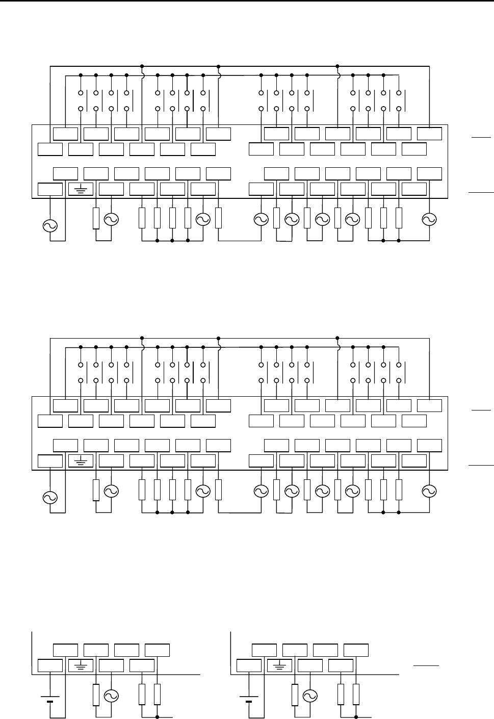
Chapter 4 Product lineup and wiring
4-14
EH-A28DR
* Since the DC input is bidirectional, it is possible to reverse the polarity of the power supply.
EH-A28EDR
* Since the DC input is bidirectional, it is possible to reverse the polarity of the power supply.
EH-D28DR EH-D28EDR
0
24+
0V 2
1
C0
3
5
4
7
6C1
AC 0
1
NC
3
2
C1
4 5
C3
6
C2 C4
7
C5
8
10 C6
11 C6
10
9
8C2
11
12
C2
14
13
C3
15 C3
9
AC C0
Input
Output
Load power supply
24V DC, 100-240V AC
Power supply
100-240V AC
Power supply
for in
p
ut 24V DC
0
24+
0V 2
1
C0
3
5
4
7
6C1
AC 16
17
NC
19
18
C1
20 21
C3
22
C2 C4
23
C5
24
26 C6
27 C6
10
9
8C2
11
12
C2
14
13
C3
15 C3
25
AC C0
Input
Output
Load power supply
24V DC, 100-240V AC
Power supply
100-240V AC
Power supply
for in
p
ut 24V DC
0V
24V C0
0
1
NC 20V
24V C0
16
17
NC 18
Output
Chapter 4 Product lineup and wiring
4-15
Analog expansion unit
EH-A6EAN (Example of voltage input and voltage output)
EH-D6EAN (Example of current input and current output)
Input and output can be configured
as voltage or current independently.
Power supply
100-240V AC
IN1JP
IN1+
IN1- IN2+
IN2-
IN3-
IN2JP
IN3JP
IN3+
IN4+
IN4- IN4JP
AC
AC OC6
NC
VO6
IO6
IO7
OC7
NC
VO7 NC
+
_+
_
Volta
g
e in
p
ut × 4
Volta
g
e out
p
ut × 2
Power supply
24V DC
IN1JP
IN1+
IN1- IN2+
IN2-
IN3-
IN2JP
IN3JP
IN3+
IN4+
IN4- IN4JP
0V
24V OC6
NC
VO6
IO6
IO7
OC7
NC
VO7 NC
Input and output can be configured
as voltage or current independently.
Current in
p
ut × 4
Current out
p
ut × 2

Chapter 4 Product lineup and wiring
4-16
4.7 Weights and Power Consumption
Power consumption (A) Remarks
100V AC 264V AC 24V DC
Type Weight
(g) Normal Rush Normal Rush Normal Rush
EH-D10DT/DTP/DR 200----0.120.6
EH-D14DT/DTP/DTPS300----0.160.6
EH-A14DR 400 0.1 15 0.06 40 - -
EH-D14DR 300----
0.16 0.6
EH-A14AS 380 0.1 15 0.06 40 - -
EH-A23DRP/DRT 600 0.2 15 0.06 40 - -
EH-D23DRP 500----
0.2 0.6
EH-D28DT/DTP/DTPS500----
0.2 0.6
EH-A28DRP/DRT 600 0.1 15 0.06 40 - -
EH-A28DR 600 0.2 15 0.06 40 - -
EH-D28DRP/DRT 500----
0.3 0.6
EH-D28DR 500----
0.3 0.6
EH-A28AS 600 0.2 15 0.06 40 - -
EH-D14EDT/EDTP/EDTPS 300 - - - - 0.16 0.6
EH-A14EDR 400 0.1 15 0.06 40 - -
EH-D14EDR 300 - - - - 0.16 0.6
EH-D28EDT/EDTPS 500 - - - - 0.2 0.6
EH-A28EDR 600 0.2 15 0.06 40 - -
EH-D28EDR 500 - - - - 0.3 0.6
EH-A6EAN 400 0.1 15 0.06 40 - -
EH-D6EAN 300 - - - - 0.16 0.6
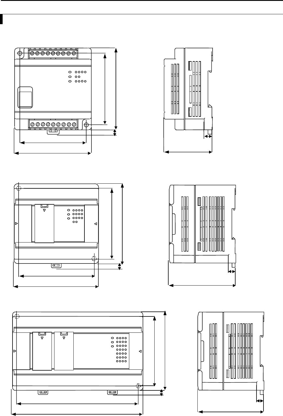
Chapter 4 Product lineup and wiring
4-17
4.8 Exterior Dimensions
(1) 10-point type
(Unit : mm)
(2) 14-point type, 14-point expansion unit, Analog expansion unit
(3) 23-point, 28-point types and 28-point expansion
75
65
47
70 80
4.4
8
95
85
80 90
76
4.8
8.4
150
140
80 90
76
4.8
8.4

Chapter 4 Product lineup and wiring
4-18
MEMO
Chapter 5 Instruction Specifications
5-1
Chapter 5 Instruction Specifications
5.1 Instruction Classifications
The instructions used with the MICRO-EH are classified as shown in the following table.
Table 5.1 Instruction classification table
No. Instruction classification Description Type
1 Basic instructions Sequence 21
Timer/counter 6
Relational box 8
2 Arithmetic instructions Substitution (array variable) 1
Mathematical operations 10
Logical operations 3
Relational expression 8
3 Application instructions Bit operation 3
Shift/rotate 8
Transfer 3
Negation/Two's complement/Sign 3
Conversion 4
Application: BCU, SWAP, UNIT, DIST 4
4 Control instructions END, JMP, CAL, FOR, NEXT, RTS, RTI, LBL, SB,
INT, CEND, CJMP
12
5 Transfer instructions TRNS 0, RECV 0 2
6 FUN instructions Refresh, high-speed counter, PMW, pulse, comments 18
5.2 List of Instructions
[Legend]
Condition codes
DER Data error (special internal output R7F4)
Set to “1” as a data error when the I/O number is exceeded or when the BCD was abnormal data, etc.
When there is no data error, it is set to “0.”
ERR Error (special internal output R7F3)
Set to “1” when an error is generated when a control instruction and a special instruction are executed.
The error code is set in WRF015. When there are no errors, the previous status is maintained.
SD Shift data (special internal output R7F2)
Performs shift-in of the contents of SD by the SHR or SHL instruction.
V Over flow (special internal output R7F1)
Indicates that a digit overflow has occurred and the signed data range is exceeded as a result of signed
data operations.
C Carry (special internal output R7F0)
Indicates the contents of digit increase due to addition, digit decrease due to subtraction, and shift-out
due to shifting.
zMaintains the previous status.
1] Set to “1” when there is an error in operation results. The previous status is maintained if there is no
error.
↕Changes according to the operation result.
Processing time This indicates the instruction processing time.
The displayed value is an average. It varies depending on the parameter and data count with the
instructions used.
See the details on the instruction specifications for details.
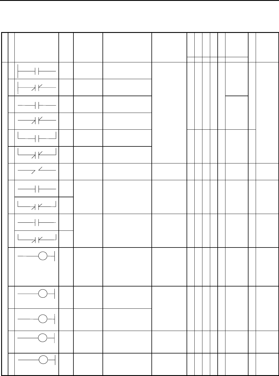
Chapter 5 Instruction Specifications
5-2
The following lists the instructions.
1. Basic instructions (sequence instructions)
R7F4
R7F3
R7F2
R7F1
R7F0
Process
time
(µs)
Classification
Item number
Ladder symbol
Instruction
symbol
Instruction
name Process descriptions I/O types used
DER ERR SD V C MICRO-EH
Steps
Remarks
1 LD Logical
operation start
Indicates the
commencement of a-
contact operation.
zzzzz 0.9 1
2 LDI Logical
negation
operation start
Indicates the
commencement of b-
contact operation.
Sequence instructions
3 AND Logical AND Indicates a-contact series
connection.
X, Y
R0 to R7BF
M0 to M3FFF
TD, SS, CU, CT
Timer: 0 to 255
Counter: 0 to 255
DIF0 to DIF511
DFN0 to
DFN511
0.8
4 ANI Logical
NAND
Indicates b-contact series
connection.
5 OR Logical OR Indicates a-contact
parallel connection.
zzzzz 0.9 2
6 ORI Logical NOR Indicates b-contact
parallel connection.
7 NOT Logical NOT Reverses all operation
results up to that point.
None zzzzz 0.8 2
8DIFAND
DIF
Leading edge
detection
Indicates detection of the
input rise.
DIF0 to DIF511
(Decimal)
zzzzz 1.0 3
4
Number
overlap not
allowed
DIF OR
DIF
9DFNAND
DFN
Trailing edge
detection
Indicates detection of the
input fall.
DFN0 to
DFN511
(Decimal)
zzzzz 1.2 3
4
Number
overlap not
allowed
DFN OR
DFN
10 OUT I/O output Indicates an output coil. X, Y
R0 to R7BF
M0 to M3FFF
TD, SS, CU,
CTU, CTD, CL
Timer: 0 to 255
Counter: 0 to 255
zzzzz 1.0 1
11
SET
SET I/O set Indicates set output. X, Y
R0 to R7BF
M0 to M3FFF
zzzzz 0.9 1
12
RES
RES I/O reset Indicates reset output.
13
MCS
MCS Set master
control
Indicates master control
set operation.
MCS0 to MCS49 zzzzz 0.7 3 Number
overlap
allowed
14
MCR
MCR Reset master
control
Indicates master control
reset operation.
MCR0 to
MCR49
zzzzz 0.7 2 Number
overlap
allowed
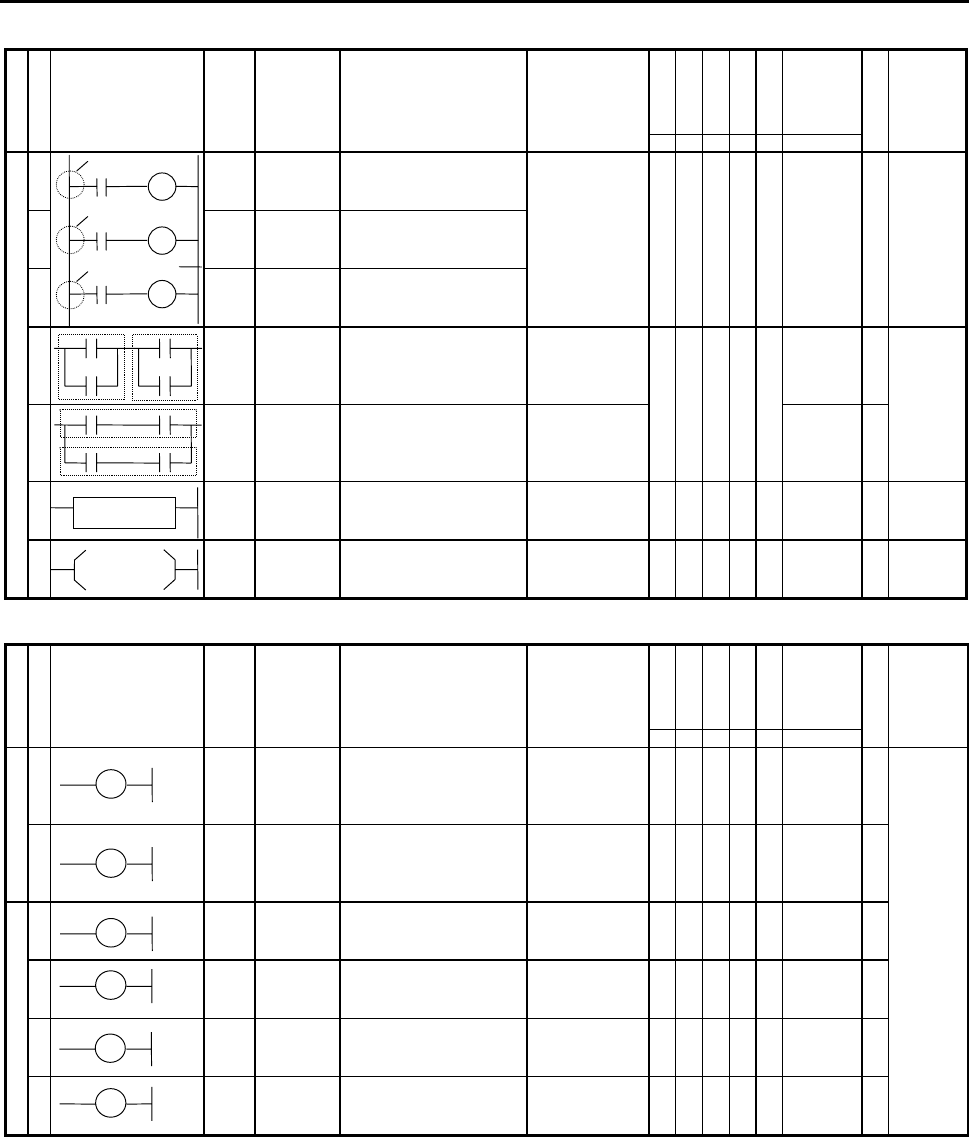
Chapter 5 Instruction Specifications
5-3
R7F4
R7F3
R7F2
R7F1
R7F0
Process
time
(µ s)
Classification
Item number
Ladder symbol
Instruction
symbol
Instruction
name Process descriptions I/O types used
DER ERR SD V C MICRO-EH
Steps
Remarks
15 MPS MPS Operation
result push
Stores the previous
operation result.
None zzzzz —0
16 MRD MRD Operation
result read
Reads the stored operation
result and continues
operation.
17 MPP MPP Operation
result pull
Reads the stored operation
result, continues operation
and clears the stored result.
Sequence instructions
18 ANB Logical
block serial
connection
Indicates serial connection
between two logical blocks.
None zzzzz —0
19 ORB Logical
block
parallel
connection
Indicates parallel
connection between two
logical blocks.
None 0.7 1
20 [ ] Processing
box start
and end
Indicates start and end of a
process box.
None zzzzz 0.6 3
21 ( ) Relational
box start
and end
Indicates start and end of a
comparison box.
None zzzzz 0.8 0
2. Basic instructions (timer, counter)
R7F4
R7F3
R7F2
R7F1
R7F0
Process
time
(µ s)
Classification
Item number
Ladder symbol
Instruction
symbol
Instruction
name Process descriptions I/O types used
DER ERR SD V C MICRO-EH
Steps
Remarks
Timer
22
TD
OUT
TD
On delay
timer
Indicates an on delay timer
operation.
TD0 to TD255
When 0.01 s, it is
possible to use
until 0 to 63.
zzzzz 1.4 5 Number
overlap not
allowed
23
SS
OUT
SS
Single shot Indicates a single shot
operation.
SS0 to SS255
When 0.01 s, it is
possible to use 0
to 63.
zzzzz 1.4 5
24
CU
OUT
CU
Counter Indicates a counter
operation.
CU0 to CU255 zzzzz 1.4 5
25
CTU
OUT
CTU
Up of
up/down
counter
Indicates an up operation of
up-down counter.
CTU0 to
CTU255
zzzzz 1.4 5
Counter
26
CTD
OUT
CTD
Down of
up/down
counter
Indicates a down operation
of up-down counter.
CTD0 to
CTD255
zzzzz 1.4 3
27
CL
OUT
CL
Counter
clear
Indicates a clear operation
for CU, RCU, CTU, CTD
and WDT.
CL0 to CL255 zzzzz 0.9 1
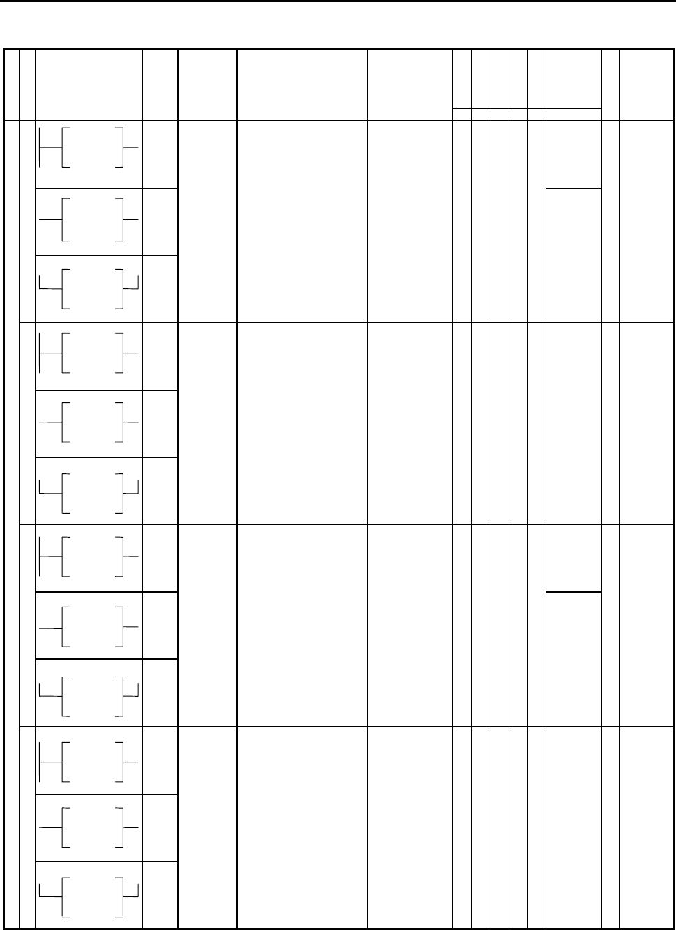
Chapter 5 Instruction Specifications
5-4
3. Basic instructions (relational box)
R7F4
R7F3
R7F2
R7F1
R7F0
Process
time
(µ s)
Classification
Item number
Ladder symbol
Instruction
symbol
Instruction
name Process descriptions I/O types used
DER ERR SD V C MICRO-EH
Steps
Remarks
Relational box
28 LD
(s1==
s2)
= Relational
box
When s1 = s2: Continuity
When s1 ≠ s2:
Noncontinuity
zzzzz 27 5
6
7
8
*1
*2
Upper
case: W
AND
(s1==
s2)
[Word]
WX, WY, WR,
WM,
Timer Counter
[Double word]
DX, DY, DR,
DM
Constant
35 Lower
case: DW
OR
(s1==
s2)
29 LD
(s1
S==
s2)
Signed =
Relational
box
When s1 = s2: Continuity
When s1 ≠ s2:
Noncontinuity
s1 and s2 are compared as
signed 32-bit binary.
DX, DY, DR,
DM
Constant
zzzzz 35 5
6
7
8
*2
AND
(s1
S==
s2)
OR
(s1
S==
s2)
30 LD
(s1<
>s2)
<>
Relational
box
When s1 = s2:
Noncontinuity
When s1 ≠ s2: Continuity
zzzzz 26.8 5
6
7
8
*1
*2
Upper
case: W
AND
(s1<
>s2)
[Word]
WX, WY, WR,
WM,
Timer Counter
[Double word]
DX, DY, DR,
DM
Constant
34.5 Lower
case: DW
OR
(s1<
>s2)
31 LD
(s1
S<>
s2)
Signed <>
Relational
box
When s1 = s2:
Noncontinuity
When s1 ≠ s2: Continuity
s1 and s2 are compared as
signed 32-bit binary.
DX, DY, DR,
DM
Constant
zzzzz 34.5 5
6
7
8
*2
AND
(s1
S<>
s2)
OR
(s1
S<>
s2)
*1: In the case of word, it requires five steps for LD (s1s2) and AND (s1s2), and six steps for OR (s1s2).
*2: In the case of double word, for LD (s1s2) and AND (s1s2), it requires five steps when the combination of s1 and s2 is I/O
and I/O, six steps when the combination is either I/O and constant or constant and I/O, and seven steps when the combination
is constant and constant. For OR (s1s2), one step is added respectively.
s1
<>
s2
s1
<>
s2
s1
<>
s2
s1
==
s2
s1
==
s2
s1
==
s2
s1
S==
s2
s1
S==
s2
s1
S==
s2
s1
S<>
s2
s1
S<>
s2
s1
S<>
s2
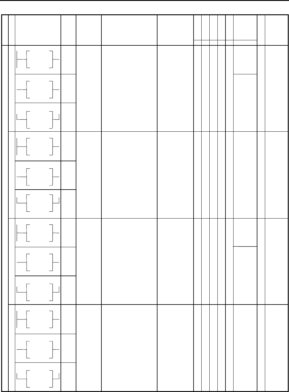
Chapter 5 Instruction Specifications
5-5
R7F4
R7F3
R7F2
R7F1
R7F0
Process
time
(µ s)
Classification
Item number
Ladder symbol
Instruction
symbol
Instruction
name Process descriptions I/O types used
DER ERR SD V C MICRO-EH
Steps
Remarks
32 LD
(s1<
s2)
< Relational
box
When s1 < s2: Continuity
When s1 ≥ s2:
Noncontinuity
zzzzz 26.8 5
6
7
8
*1
*2
Upper
case: W
Relational box
AND
(s1<
s2)
[Word]
WX, WY, WR,
WM,
Timer Counter
[Double word]
DX, DY, DR,
DM
Constant
37.5 Lower
case: DW
OR
(s1<
s2)
33 LD
(s1
S<
s2)
Signed <
Relational
box
When s1 < s2: Continuity
When s1 ≥ s2:
Noncontinuity
s1 and s2 are compared as
signed 32-bit binary.
DX, DY, DR,
DM
Constant
zzzzz 37.5 5
6
7
8
*2
AND
(s1
S<
s2)
OR
(s1
S<
s2)
34 LD
(s1
<=
s2)
<=
Relational
box
When s1 ≤ s2:
Noncontinuity
When s1 > s2: Continuity
zzzzz 26.8 5
6
7
8
*1
*2
Upper
case: W
AND
(s1
<=
s2)
[Word]
WX, WY, WR,
WM,
Timer Counter
[Double word]
DX, DY, DR,
DM
Constant
42 Lower
case: DW
OR
(s1
<=
s2)
35 LD
(s1
S<=
s2)
Signed <=
Relational
box
When s1 ≤ s2: Continuity
When s1 > s2:
Noncontinuity
s1 and s2 are compared as
signed 32-bit binary.
DX, DY, DR,
DM
Constant
zzzzz 37.5 5
6
7
8
*2
AND
(s1
S<=
s2)
OR
(s1
S<=
s2)
*1: In the case of word, it requires five steps for LD (s1s2) and AND (s1s2), and six steps for OR (s1s2).
*2: In the case of double word, for LD (s1s2) and AND (s1s2), it requires five steps when the combination of s1 and s2 is I/O
and I/O, six steps when the combination is either I/O and constant or constant and I/O, and seven steps when the combination
is constant and constant. For OR (s1s2), one step is added respectively.
s1
<
s2
s1
<
s2
s1
<
s2
s1
<=
s2
s1
<=
s2
s1
<=
s2
s1
S<
s2
s1
S<
s2
s1
S<
s2
s1
S<=
s2
s1
S<=
s2
s1
S<=
s2

Chapter 5 Instruction Specifications
5-6
4. Arithmetic instructions
R7F4
R7F3
R7F2
R7F1
R7F0
Process
time
(µ s)
Classification
Item number
Ladder symbol
Instruction
symbol
Instruction
name Process descriptions I/O types used
DER ERR SD V C MICRO-EH
Steps
Remarks
1 d=s Substitution d ← s [Bit] ↕zzzz 32 3 I/O: I/O
statement d: Y, R, M 74 4 I/O: Array
s: X, Y, R, M, 52 4 Array: I/O
Constant 92 5 Array:
Array
[Word] ↕zzzz 27 3 I/O: I/O
d: WY, WR, 66 4 I/O: Array
WM, Timer ·
Counter 53 4 Array: I/O
Substitution statement
s: WX, WY, WR,
WM, Timer · 99 5 Array:
Counter,
Constant
Array
[Double word] ↕zzzz 35 4 I/O: I/O
d: DY, DR, 86 4 I/O: Array
DM
s: DX, DY, DR, 71 5 Array: I/O
DM, Constant
* Array variables
can be used.
120 5 Array:
Array
2 d=s1+s2 Binary
addition
d ← s1+s2 zzz ↕↕ 45
61
4
6
Upper
case: W
Lower
case: DW
3d=s1 B+ s2 BCD
addition
d ← s1+s2 ↕zzz ↕115
177
4
6
Upper
case: W
Lower
case: DW
Mathematical operation
4 d=s1 - s2 Binary
subtraction
d ← s1 - s2 zzz ↕↕ 41
58
4
6
Upper
case: W
Lower
case: DW
5d=s1 B - s2 BCD
subtraction
d ← s1 - s2
[Word]
d: WY, WR, WM
s1, s2: WX, WY,
WR, WM, Timer
Counter,
Constant
[Double word]
d: DY, DR, DM
s1, s2: DX, DY,
DR, DM,
Constant
↕zzz ↕104
163
4
6
Upper
case: W
Lower
case: DW
6d=s1 x s2 Binary
multiplication
d ← s1 x s2 ↕zzzz 43
112
4
6
Upper
case: W
Lower
case: DW
7d=s1 B x s2 BCD
multiplication
d ← s1 x s2 ↕zzzz 164
447
4
6
Upper
case: W
Lower
case: DW
8d=s1 S x s2 Signed binary
multiplication
d ← s1 x s2 [Double word]
d: DY, DR, DM
s1, s2: DX, DY,
DR, DM,
Constant
↕zzzz 143 6
9 d=s1 / s2 Binary
division
[Word]
d ← s1 / s2
WRF016 ← s1 mod s2
[Word]
d: WY, WR, WM
s1, s2: WX, WY,
WR, WM,
↕zzzz 55
110
4
6
Upper
case: W
Lower
case: DW
10 d=s1 B/ s2 BCD
division
[Double word]
d ← s1 / s2
DRF016 ← s1 mod s2
Timer Counter,
Constant
[Double word]
d: DY, DR,, DM
s1, s2: DX, DY,
DR, DM,
Constant
152
253
4
6
Upper
case: W
Lower
case: DW
11 d=s1 S/ s2 Signed
binary
division
[Double word]
d: DY, DR, DM
s1, s2: DX, DY,
DR, DM,
Constant
↕zz ↕z101 6

Chapter 5 Instruction Specifications
5-7
R7F4
R7F3
R7F2
R7F1
R7F0
Process
time
(µ s)
Classification
Item number
Ladder symbol
Instruction
symbol
Instruction
name Process descriptions I/O types used
DER ERR SD V C MICRO-EH
Steps
Remarks
Logic operation
12 d=s1 OR s2 Logical OR d ← s1+s2 zzzzz 62
33
86
4
4
6
Upper
case: B
Middle
case: W
Lower
case: DW
13 d=s1 AND s2 Logical
AND
d ← s1 x s2 zzzzz 46
36
49
4
4
6
Upper
case: B
Middle
case: W
Lower
case: DW
14 d=s1 XOR s2 Exclusive
OR
d ← s1 ⊕ s2
[Bit]
d: Y, R, M
s1, s2: X, Y, R,
M
[Word]
d: WY, WR,
WM,
Timer Counter
s1, s2: WX, WY,
WR, WM, Timer
Counter, Constant
[Double word]
d: DY, DR, DM
s1, s2: DX, DY,
DR, DM,
Constant
zzzzz 42
33
66
4
4
6
Upper
case: B
Middle
case: W
Lower
case: DW
Relational expression
15 d=s1 == s2 = Relational
expression
When s1 = s2, d ← 1
When s1 ≠ s2, d ← 0
[Word]
d: Y, R, M
s1, s2: WX, WY,
WR, WM, Timer
Counter, Constant
[Double word]
d: Y, R, M
s1, s2: DX, DY,
DR, DM,
Constant
zzzzz 60
48
4
6
Upper
case: W
Lower
case: DW
16 d=s1 S== s2 Signed =
Relational
expression
When s1 = s2, d ← 1
When s1 ≠ s2, d ← 0
s1 and s2 are compared as
signed 32-bit binary.
[Double word]
d: Y, R, M
s1, s2: DX, DY,
DR, DM,
Constant
108 6
17 d=s1<>s2 <>
Relational
expression
When s1 = s2, d ← 0
When s1 ≠ s2, d ← 1
[Word]
d: Y, R, M
s1, s2: WX, WY,
WR, WM, Timer ·
Counter, Constant
[Double word]
d: Y, R, M
s1, s2: DX, DY,
DR, DM,
Constant
zzzzz 60
46
4
6
Upper
case: W
Lower
case: DW
18 d=s1 S<> s2 Signed <>
Relational
expression
When s1 = s2, d ← 0
When s1 ≠ s2, d ← 1
s1 and s2 are compared as
signed 32-bit binary.
[Double word]
d: Y, R, M
s1, s2: DX, DY,
DR, DM,
Constant
48 6
19 d=s1<s2 < Relational
expression
When s1 < s2, d ← 1
When s1 ≥ s2, d ← 0
[Word]
d: Y, R, M
s1, s2: WX, WY,
WR, WM, Timer
Counter, Constant
[Double word]
d: Y, R, M
s1, s2: DX, DY,
DR, DM,
Constant
zzzzz 40
70
4
6
Upper
case: W
Lower
case: DW
20 d=s1 S< s2 Signed <
Relational
expression
When s1 < s2, d ← 1
When s1 ≥ s2, d ← 0
s1 and s2 are compared as
signed 32-bit binary.
[Double word]
d: Y, R, M
s1, s2: DX, DY,
DR, DM,
Constant
50 6
Chapter 5 Instruction Specifications
5-8
R7F4
R7F3
R7F2
R7F1
R7F0
Process
time
(µ s)
Classification
Item number
Ladder symbol
Instruction
symbol
Instruction
name Process descriptions I/O types used
DER ERR SD V C MICRO-EH
Steps
Remarks
Relational expression
21 d=s1 <= s2 ≤ Relational
expression
When s1 < s2, d ← 1
When s1 ≥ s2, d ← 0
[Word]
d: Y, R, M
s1, s2: WX, WY,
WR, WM, Timer
Counter,
Constant
[Double word]
d: Y, R, M
s1, s2: DX, DY,
DR, DM,
Constant
zzzzz 40
71
4
6
Upper
case: W
Lower
case: DW
22 d=s1 S<= s2 Signed ≤
Relational
expression
When s1 ≤ s2, d ← 1
When s1 > s2, d ← 0
s1 and s2 are compared as
signed 32-bit binary.
[Double word]
d: Y, R, M
s1, s2: DX, DY,
DR, DM,
Constant
50 6
5. Application instructions
R7F4
R7F3
R7F2
R7F1
R7F0
Process
time
(µ s)
Classification
Item number
Ladder symbol
Instruction
symbol
Instruction
name Process descriptions I/O types used
DER ERR SD V C MICRO-EH
Steps
Remarks
1 BSET(d, n) Bit set n 0
d
Sets 1 to bit n.
zzzzz 26
35
3
3
Upper
case: W
Lower
case: DW
2 BRES(d, n) Bit reset n 0
d
Sets 0 to bit n.
zzzzz 29
38
3
3
Upper
case: W
Lower
case: DW
Bit operations
3BTS(d, n) Bit test n 0
d
Acquires the value in bit n
to C (R7F0).
[Word]
d: WY, WR,
WM, TC
n(0-15): WX,
WY, WR, WM,
TC,
Constant
[Double word]
d: DY, DR, DM
n(0-31): WX,
WY, WR, WM,
TC,
Constant
zzzz ↕31
38
3
3
Upper
case: W
Lower
case: DW
4 SHR(d, n) Shift right
Shifts right by n bits.
zzzz ↕38
46
3
3
Upper
case: W
Lower
case: DW
Shift/rotate
5 SHL(d, n) Shift left
Shifts left by n bits.
[Word]
d: WY, WR,
WM, TC
n: WX, WY, WR,
WM, TC,
Constant
zzzz ↕38
46
3
3
Upper
case: W
Lower
case: DW
6 ROR(d, n) Rotate right
Rotates right by n bits.
[Double word]
d: DY, DR, DM
n: WX, WY, WR,
WM, TC,
Constant
zzzz ↕47
75
3
3
Upper
case: W
Lower
case: DW
7 ROL(d, n) Rotate left
Rotates left by n bits.
*C: R7F0
SD: R7F2
zzzz ↕46
54
3
3
Upper
case: W
Lower
case: DW
8 LSR(d, n) Logical
shift right
Shifts right by n bits.
zzzz ↕36
45
3
3
Upper
case: W
Lower
case: DW
9 LSL(d, n) Logical
shift left
Shifts left by n bits.
zzzz ↕36
45
3
3
Upper
case: W
Lower
case: DW
0
C
C
d→
Cd
←
0C
d→→
0
Cd
←←
1
SD C
d→→
CSD
d←←
Chapter 5 Instruction Specifications
5-9
R7F4
R7F3
R7F2
R7F1
R7F0
Process
time
(µ s)
Classification
Item number
Ladder symbol
Instruction
symbol
Instruction
name Process descriptions I/O types used
DER ERR SD V C MICRO-EH
Steps
Remarks
Shift/rotate
10 BSR(d, n) BCD shift
right
Shifts BCD to right by n
digits.
[Word]
d: WY, WR, WM,
TC
n: WX, WY, WR,
WM, TC,
Constant
zzzzz 32
40
3
3
Upper
case: W
Lower
case: DW
11 BSL(d, n) BCD shift
left
Shifts BCD to left by n
digits.
[Double word]
d: DY, DR, DM
n: WX, WY, WR,
WM, TC,
constant
zzzzz 32
39
3
3
Upper
case: W
Lower
case: DW
Transfer
12 MOV(d, s, n) Block
transfer
Transfers (copies) n bits (or
words) of data from I/O
number s to the n bit (or
word) range from I/O
number s.
[Bit]
d, s: R, M
n(0-255): WX,
WY, WR, WM,
TC, Constant
↕zzzz 153 4 *3
Upper
case: B
[Word]
d, s: WR, WM
n(0-255):WX,
WY, WR, WM,
TC, Constant
124 4 Lower
case: W
13 COPY(d, s, n) Copy Copies the bit (or word)
data of I/O number s to the
n bit (or word) range from
I/O number d.
[Bit]
d: R, M
s: X, Y, R, M,
Constant
n(0-255): WX,
WY, WR, WM,
TC, Constant
↕zzzz 80 4 *3
Upper
case: B
[Word]
d: WR, WM
s, n(0-255): WX,
WY, WR, WM,
TC, Constant
73 4 Lower
case: W
14 XCG(d1, d2, n) Block
exchange
Exchanges the n bit (or
word) range from I/O
number d1 and the n bit (or
word) range from I/O
number d2.
[Bit]
d1, d2: R, M
n(0-255): WX,
WY, WR, WM,
TC, Constant
↕zzzz 139 4 *3
Upper
case: B
[Word]
d: WR, WM
n(0-255): WX,
WY, WR, WM,
TC,
Constant
120 4 Lower
case: W
15 NOT(d) Reverse Reverses the bit for the I/O
number d value.
[Bit]
Y, R, M
zzzzz 27 2 Upper
case: B
[Word]
WY, WR, WM
22 2 Middle
case: W
Negation / Two's complement / Sign
[Double word]
DY, DR, DM
28 2 Lower
case: DW
16 NEG(d) Two's
complement
Stores two's complement of
the value stored in I/O
number d, in d.
[Word]
WY, WR, WM
zzzzz 22 2 Upper
case: W
[Double word]
DY, DR, DM
29 2 Lower
case: DW
17 ABS(d, s) Absolute
value
zzzz ↕30 3 Upper
case: W
Stores the absolute value of
s in d, and the sign value of
s in carry (R7F0).
(0: Positive, 1: Negative)
41 4 Lower
case: DW
[Word]
d: WY, WR, WM
s: WX, WY, WR,
WM, TC,
Constant
[Double word]
d: DY, DR, DM
s: DX, DY, DR,
DM, Constant
d
0→
d
←0

Chapter 5 Instruction Specifications
5-10
R7F4
R7F3
R7F2
R7F1
R7F0
Process
time
(µ s)
Classification
Item number
Ladder symbol
Instruction
symbol
Instruction
name Process descriptions I/O types used
DER ERR SD V C MICRO-EH
Steps
Remarks
Conversion
18 BCD(d, s) Binary →
BCD
conversion
Converts the value of s into
BCD and stores it in I/O
number d. If the value of s
is an error, DER (R 7F4) =
1 is set.
[Word]
d: WY, WR, WM
s: WX, WY, WR,
WM, TC,
Constant
↕zzzz 79
89
3
4
Upper
case: W
Lower
case: DW
19 BIN(d, s) BCD →
Binary
conversion
Converts the value of s into
binary and stores it in I/O
number d. If the value of s
is an error, DER (R 7F4) =
1 is set.
[Double word]
d: DY, DR, DM
s: DX, DY, DR,
DM, Constant
↕zzzz 49
75
3
4
Upper
case: W
Lower
case: DW
20 DECO(d, s, n) Decode Decodes the value indicated
by the least significant n
bits of s, and sets the bit
that corresponds to the
decoding result of the bit
row starting from I/O
number d, to 1.
d: R, M
s: WX, WY, WR,
WM, TC,
Constant
n: Constant(1-8)
↕zzzz 105 4 *3
21 ENCO(d, s, n) Encode Encodes the bit location in
which 1 is set within the bit
row, which starts with I/O
number s and lasts for the
amount of nth power of 2,
and stores it in I/O number
d. If multiple bits that
contain 1 exist, the one
with the upper bit locations
will be encoded.
d: WY, WR, WM
s: R, M
n: Constant(1-8)
↕zzz ↕128 4 *3
*3: Processing time when n=1.
R7F4
R7F3
R7F2
R7F1
R7F0
Process
time
(µ s)
Classification
Item number
Ladder symbol
Instruction
symbol
Instruction
name Process descriptions I/O types used
DER ERR SD V C MICRO-EH
Steps
Remarks
22 BCU(d, s) Bit count Among the contents of s
(word, double-word), stores
the number of bits that are
set to 1 in I/O number d.
[Word]
d: WY, WR, WM
s: WX, WY, WR,
WM, TC,
Constant
zzzzz 33 3 Upper
case: W
[Double word]
d: WY, WR, WM
s: DX, DY, DR,
DM, Constant
42 4 Lower
case: DW
Application instruction
23 SWAP(d) Swap Swaps the upper 8 bits and
the lower 8 bits of the value
(word) for I/O number d.
d: WY, WR, WM zzzzz 25 2
24 UNIT(d, s, n) Unit Stores the lower 4 bit
values of the n words
starting with s in the lower
4 bits each of d (word).
d: WY, WR, WM
s: WR, WM
n: Constant(0-4)
↕zzzz 100 4 *4
25 DIST(d, s, n) Distribute Extracts the value of s
(word) in 4 bit units from
the least significant bits,
and sets them in the lower 4
bits of each word starting
with I/O number d (word).
The upper bits are set to 0.
d: WR, WM
s: WX, WY, WR,
WM, TC,
Constant
n: Constant(0-4)
↕zzzz 87 4 *4
*4: Processing time when n = 1

Chapter 5 Instruction Specifications
5-11
6. Control instructions
R7F4
R7F3
R7F2
R7F1
R7F0
Process
time
(µ s)
Classification
Item number
Ladder symbol
Instruction
symbol
Instruction
name Process descriptions I/O types used
DER ERR SD V C MICRO-EH
Steps
Remarks
1END Normal
scan end
Indicates the end of a
normal scan.
None zzzzz 714 1
Control
2 CEND(s) Scan
conditional
end
Re-executes normal scan
from the beginning of the
normal scan when s=1,
while the next instruction is
executed when s=0.
s: X, Y, R, M zzzzz
3 JMP n Unconditio-
nal jump
Jumps to LBL n of the
same No. n.
n: Constant(0-
255)
z1] zzz
5
707
32
2
2
*5
*6
4 CJMP n (s) Conditional
jump
When s=1, jumps to the
LBL n of the same No.;
when s=0, executes the next
instruction.
n: Constant(0-
255)
s: X, Y, R, M
z1] zzz 3
32
3*5
*6
5 LBL n Label Indicates the jump
destination of JMP or
CJMP of the same No.
n: Constant(0-
255)
zzzzz 0.5 1
6 FOR n (s) FOR When s=0, jumps to the
location after the NEXT n
of the same No.; when s is
not 0, executes the next
instruction.
n: Constant(0-49)
s: WY, WR, WM
z1] zzz 33 3
7 NEXT n NEXT Subtracts 1 from the s value
of the FOR n of the same
No. and jumps to FOR n.
n: Constant(0-49) z1] zzz 38 2
8CAL n Call
subroutine
Executes the SB n
subroutine of the same No.
n.
n: Constant(0-99) z1] zzz 24 2
9SB n Start
subroutine
Indicates the start of No. n
subroutine.
n: Constant(0-99) z1] zzz 0.5 1
10 RTS RETURN
SUBROUTIN
Returns from subroutine. None zzzzz 25 1
11 INT n Start
interrupt
scan
Indicates the start of No. n
interrupt scan.
n: Constant(0-2,
16-19, 20-27)
zzzzz 0.5 1
12 RTI RETURN
INTERRUPT
Returns from interrupt
scan.
None zzzzz 0.5 1
7. Transfer instructions
R7F4
R7F3
R7F2
R7F1
R7F0
Process
time
(µ s)
Classification
Item number
Ladder symbol
Instruction
symbol
Instruction
name Process descriptions I/O types used
DER ERR SD V C MICRO-EH
Steps
Remarks
1 TRNS 0 Data sending and receiving
(optional)
d: WY10
s: WR, WM
t: R, M
↕zzzz 80 3
Transfer inst.
2RECV 0
General
purpose
port
communica
-tion
command
Data receiving and sending
(optional)
d: WX0
s: WR, WM
t: R, M
↕zzzz 80 3
8. FUN instructions
R7F4
R7F3
R7F2
R7F1
R7F0
Process
time
(µ s)
Classification
Item number
Ladder symbol
Instruction
symbol
Instruction
name Process descriptions I/O types used
DER ERR SD V C MICRO-EH
Steps
Remarks
1 FUN 5 (s) General
purpose
port
switching
Port type switching from
dedicated port to general
purpose port
s: WR,WM ↕zzzz 114 3
2 FUN 80 (s)
(ALREF (s))
I/O refresh
(all points)
Refreshes all external I/O
ranges.
s: WR,WM ↕zzzz 432 3
FUN instructions
3 FUN 81 (s)
(IOREF (s))
I/O refresh
(I/O /link
designation
)
Refreshes only the input
range, output range or link
range.
s: WR,WM ↕zzzz 244 3

Chapter 5 Instruction Specifications
5-12
R7F4
R7F3
R7F2
R7F1
R7F0
Process
time
(µ s)
Classification
Item number
Ladder symbol
Instruction
symbol
Instruction
name Process descriptions I/O types used
DER ERR SD V C MICRO-EH
Steps
Remarks
4 FUN 82 (s)
(SLREF (s))
I/O refresh
(any slot)
Refreshes the I/O at the
designated slot.
s: WR, WM ↕zzzz 311 3
5 FUN 140 (s) High-speed
counter
operation
control
Performs the starting and
stopping of the count
operation of the specified
counter.
s: WR, WM ↕zzzz 147 3
FUN instructions
6 FUN 141 (s) High-speed
counter
coincidence
output
control
Performs the enabling and
disabling of the coincidence
output of the specified
counter.
s: WR, WM ↕zzzz 138 3
7 FUN 142 (s) High-speed
counter up-
count /
down-count
control
This controls the up-
count/down-count of the
specified counter. (Single-
phase counters only)
s: WR, WM ↕zzzz 156 3
8 FUN 143 (s) High-speed
counter
current value
replacement
The counter value of the
specified counter number
will be replaced by the data
stored in the replacement
value storage area.
s: WR, WM
s+1: WR, WM
↕zzzz 175 3
9 FUN 144 (s) High-speed
counter
current
value
reading
This function reads the
count value of the specified
counter number and writes
it to the current value
storage range
s: WR, WM
s+1: WR, WM
↕zzzz 132 3
10 FUN 145 (s) High-speed
counter
current
value clear
Clears the count value of the
specified counter number.
s: WR, WM ↕zzzz 157 3
11 FUN 146 (s) High-speed
counter
preset
The on-preset value and
off-preset value will be set
according to the preset
specifications in respect to
the specified counter
number.
s: WR, WM
s+1: WR, WM
s+2: WR, WM
↕zzzz 162 3
12 FUN 147 (s) PWM
operation
control
Starts PWM output of the
specified PWM output
number.
s: WR, WM ↕zzzz 135 3
13 FUN 148 (s) PWM
Frequency
on-duty
changes
Sets the frequency value
and the on-duty value of the
PWM output number
specified by the on-duty
value and the specified
frequency value.
s: WR, WM
s+1: WR, WM
s+2: WR, WM
↕zzzz 173 3
14 FUN 149 (s) Pulse
output
control
Starts pulse output of the
specified pulse number and
the output is stopped when
the specified number of
pulses are output.
s: WR, WM ↕zzzz 149 3
15 FUN 150 (s) Pulse
frequency
output
setting
changes
Pulse output is commenced
at the specified frequency.
Output is stopped when the
number of pulses specified
have been output.
s: WR, WM
s+1: WR, WM
s+2: WR, WM
↕zzzz 217 3
16 FUN 151 (s) Pulse output
with
acceleration
/
deceleration
Divides the time band and
frequency into 10 levels
and performs
acceleration/deceleration.
s: WR, WM
s+1: WR, WM
s+2: WR, WM
s+3: WR, WM
s+4: WR, WM
↕zzzz 919 3
17 FUN 254 (s)
(BOXC (s))
BOX
comment
No processing is performed
in the CPU.
s: WR, WM zzzzz —3
18 FUN 255 (s)
(MEMC (s))
Memo
comment
No processing is performed
in the CPU.
zzzzz —3

Chapter 5 Instruction Specifications
5-13
5.3 Instruction Specification Details
(1) Basic instructions
(2) Arithmetic instructions
(3) Application instructions
(4) Control instructions
(5) Transfer instructions
(6) FUN instructions
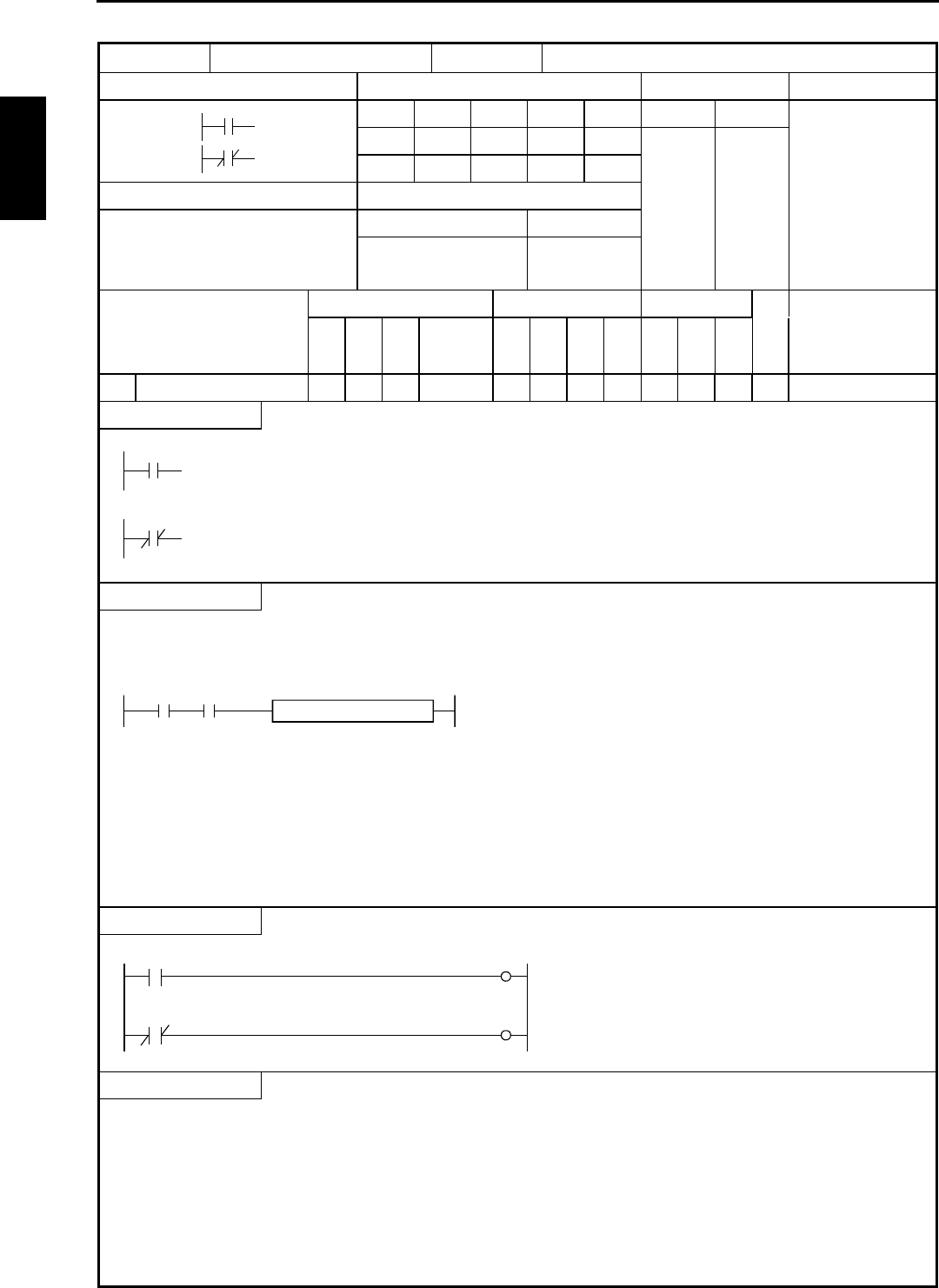
Chapter 5 Instruction Specifications
5-14
Item number Basic instructions-1, 2 Name Logical operation start (LD, LDI)
Ladder format Condition code Processing time (µs) Remark
R7F4 R7F3 R7F2 R7F1 R7F0 Average Maximum
DER ERR SD V C
n
n
zzzzz
Instruction format Number of steps 0.9 ←
LD n Condition Steps
LDI n — 1
Bit Word Double word
Usable I/O XY
R,
M
TD, SS,
CU, CT WX WY
WR,
WM TC DX DY
DR,
DM
Constant
Other
n I/O number {{{ {
Function
n
LD n
Starts the a-contact logical operation. Enters the continuity state when input is on.
n
LDI n
Starts the b-contact logical operation. Enters the continuity state when input is off.
Notes
•Edge detection (DIF, DFN) cannot be used in respect to LDI.
•Pay close attention if the external output is to be monitored when counter input (coincidence output), PWM output or pulse
output is set with the PI/O function.
Y100
WR0 = WR0 + 1
DIF1
Y100 will not change while monitored. It will remain the same value previously set using functions such as
set/reset.
For example, if Y100 is off, the Y100 status will not change while being monitored and WRO will also remain
unchanged.
Program example
X00000
X00001
Y00100
Y00101
LD
OUT
LDI
OUT
X00000
Y00100
X00001
Y00101
Program description
•When input X00000 is on, output Y00100 is on; when off, the output is off.
•When input X00001 is off, output Y00101 is on; when on, the output is off.
LD n
LDI n
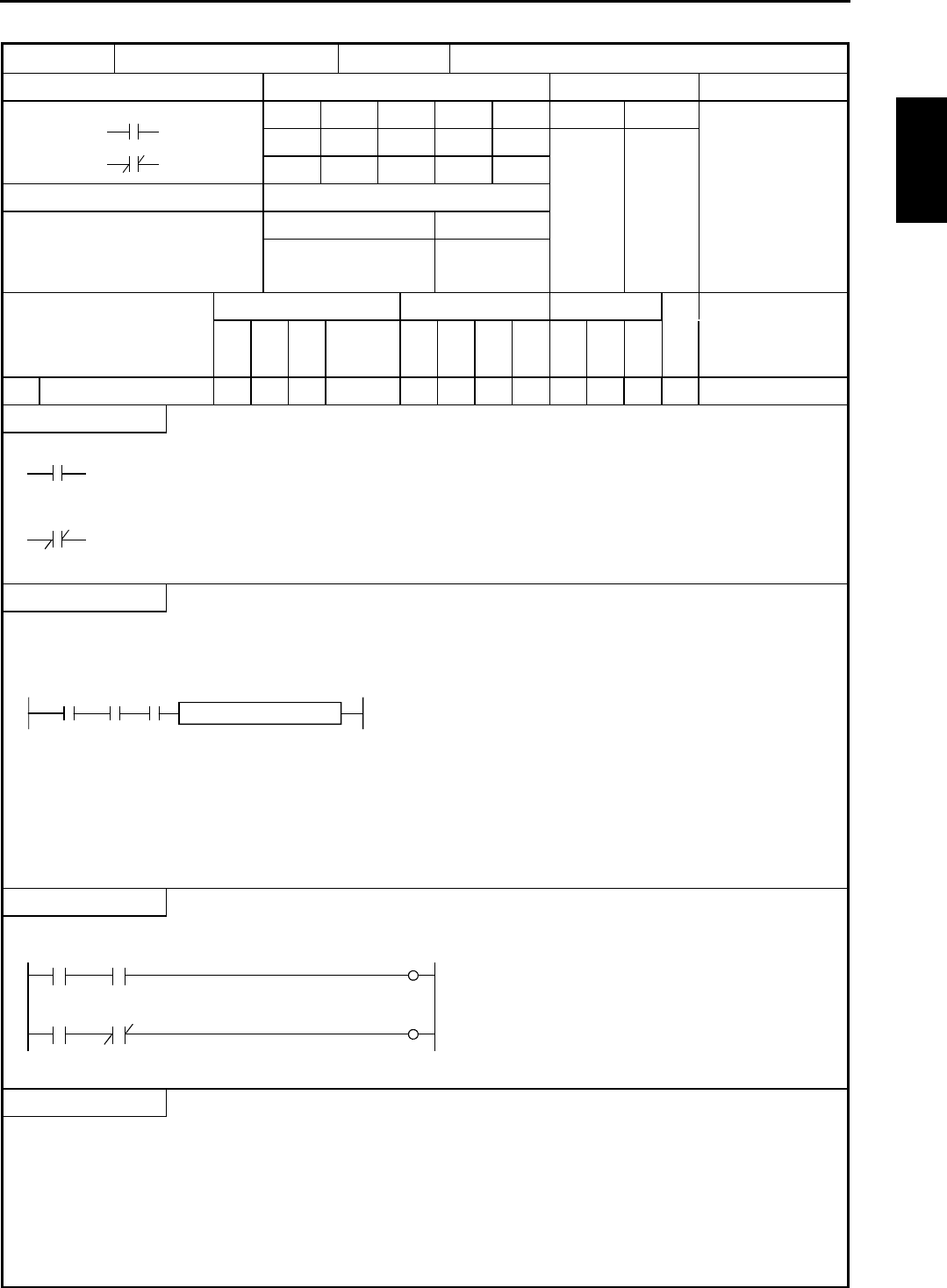
Chapter 5 Instruction Specifications
5-15
Item number Basic instructions-3, 4 Name Contact serial connection (AND, ANI)
Ladder format Condition code Processing time (µs) Remark
R7F4 R7F3 R7F2 R7F1 R7F0 Average Maximum
DER ERR SD V C
n
n
zzzzz
Instruction format Number of steps 0.8 ←
AND n Condition Steps
ANI n 1
Bit Word Double word
Usable I/O XY
R,
M
TD, SS,
CU, CT WX WY
WR,
WM TC DX DY
DR,
DM
Constant
Other
n I/O number {{{ {
Function
n
AND n
Obtains AND of the previous operation result and the a-contact operation.
n
ANI n
Obtains AND of the previous operation result and the b-contact operation.
Notes
•Edge detection (DIF, DFN) cannot be used in respect to ANI.
•Pay close attention if the external output is to be monitored when counter input (coincidence output), PWM output, or pulse
output is set with the PI/O function.
R0
WR0 = WR0 + 1
Y100 DIF1
Y100 will not change when monitored. It will remain the same value previously set using functions such as
set/reset.
For example, if Y100 is off, the Y100 status will not change while being monitored and WRO will also remain unchanged.
Program example
X00002
X00003
Y00100
Y00101
LD
AND
OUT
LD
ANI
OUT
X00002
R010
Y00100
X00003
R011
Y00101
R011
R010
Program description
•When input X00002 and R010 are both on, output Y00100 is on and all others are off.
•When input X00003 is on and R011 is off, output Y00101 is on and all others are off.
AND n
ANI n

Chapter 5 Instruction Specifications
5-16
Item number Basic instructions-5, 6 Name Contact parallel connection (OR, ORI)
Ladder format Condition code Processing time (µs) Remark
R7F4 R7F3 R7F2 R7F1 R7F0 Average Maximum
DER ERR SD V C
n
n
zzzzz
Instruction format Number of steps 0.9 ←
OR n Condition Steps
ORI n 2
Bit Word Double word
Usable I/O XY
R,
M
TD, SS,
CU, CT WX WY
WR,
WM TC DX DY
DR,
DM
Constant
Other
n I/O number {{{ {
Function
n
OR n
Obtains OR of the previous operation result and the a-contact operation.
n
ORI n
Obtains OR of the previous operation result and the b-contact operation.
Notes
•Edge detection (DIF, DFN) cannot be used in respect to ORI.
•Pay close attention if the external output is to be monitored when counter input (coincidence output), PWM output, or pulse
output is set with the PI/O function.
R0
WR0 = WR0 + 1
DIF1
Y100
Y100 will not change when monitored. It will remain the same value previously set using functions such as
set/reset.
For example, if Y100 is off, the Y100 status will not change while being monitored and WRO will also remain unchanged.
Program example
X00000
X00001
Y00105
LD
OR
ORI
OUT
X00000
X00001
X00002
Y00105
X00002
Program description
•When X00000 is on, X00001 is on, or X00002 is off, the operation is “1” and Y00105 turns on.
OR n
ORI n
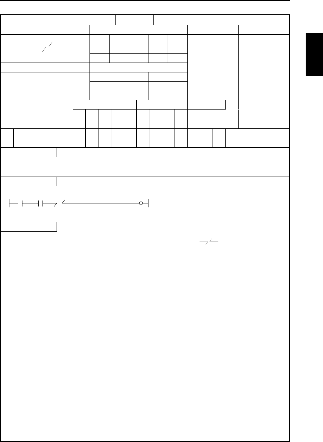
Chapter 5 Instruction Specifications
5-17
Item number Basic instructions-7 Name Negation (NOT)
Ladder format Condition code Processing time (µs) Remark
R7F4 R7F3 R7F2 R7F1 R7F0 Average Maximum
DER ERR SD V C
zzzzz
Instruction format Number of steps 0.8
Condition Steps
NOT 2
Bit Word Double word
Usable I/O XY
R,
M
TD, SS,
CU, CT WX WY
WR,
WM TC DX DY
DR,
DM
Constant
Other
Function
•Reverses the operation result obtained up to that point.
Program example
X00000 R100 LD
AND
N
OT
OUT
X00000
X00001
R100
X00001
Program description
•When input X00000 and input X00001 are both on, the operation is “1,” but due to , the calculation turns into “0”
and R100 turns off.
•In all other cases, R100 turns on.
NOT
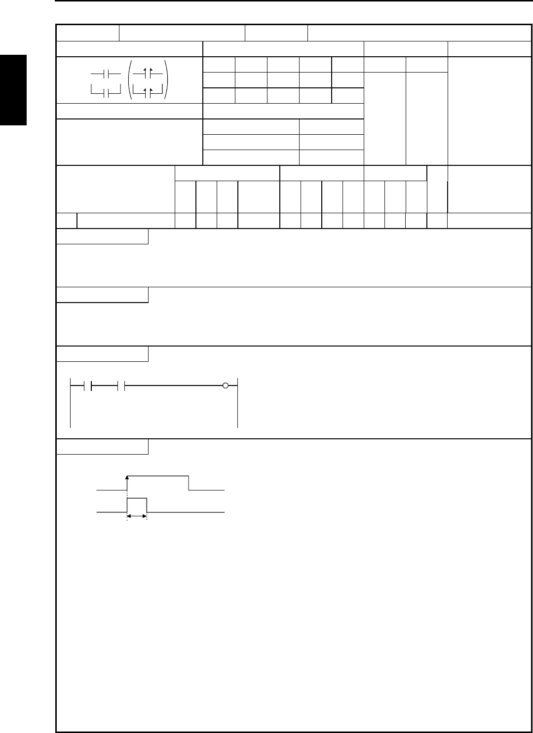
Chapter 5 Instruction Specifications
5-18
Item number Basic instructions-8 Name Leading edge detection (AND DIF, OR DIF)
Ladder format Condition code Processing time (µs) Remark
R7F4 R7F3 R7F2 R7F1 R7F0 Average Maximum
DER ERR SD V C
DIF n
DIF n
DIF n
DIF n
zzzzz
Instruction format Number of steps 1.0 ←
AND DIF n Condition Steps
OR DIF n AND DIF n 3
OR DIF n 4
Bit Word Double word
Usable I/O XY
R,
M
TD, SS,
CU, CT WX WY
WR,
WM TC DX DY
DR,
DM
Constant
Other
n Number {0 to 511 (Decimal)
Function
•Detects the rise of an input signal and retains the operation result only for one scan.
( ) indicates the display when the Ladder Editor is used.
Notes
•DIF number may not be overlapped. (However, no error is generated even if overlapped numbers are used.)
•DIF cannot use the b contact.
Program example
X00000 R123 LD
AND
OUT
X00000
DIF0
R123
DIF0
Program description
X
00000
R
123
1 scan time
Time chart
•Upon leading of X00000 on, R123 turns on only for one scan.
•If b-contact is used for X00000, operation will be the same as the a-contact DFN operation.
AND DIF n
OR DIF n
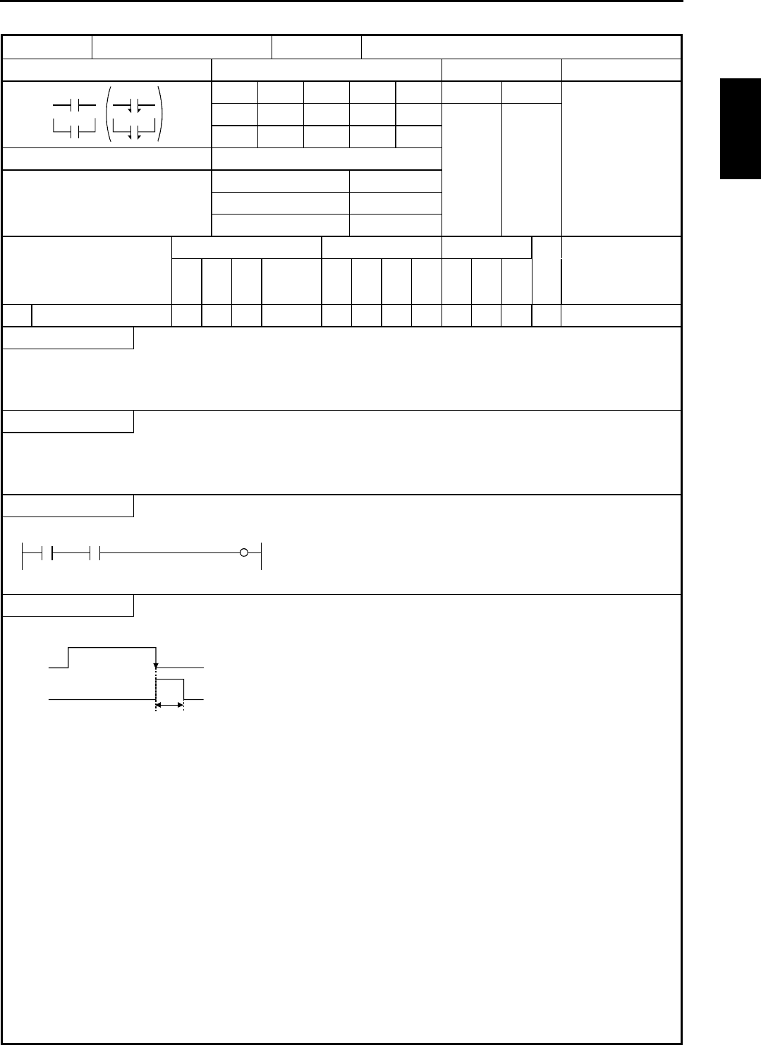
Chapter 5 Instruction Specifications
5-19
Item number Basic instructions-9 Name Trailing edge detection (AND DFN, OR DFN)
Ladder format Condition code Processing time (µs) Remark
R7F4 R7F3 R7F2 R7F1 R7F0 Average Maximum
DER ERR SD V C
DFN n
DFN n
DFN n
DFN n
zzzzz
Instruction format Number of steps 1.0 ←
AND DFN n Condition Steps
OR DFN n AND DFN n 3
OR DFN n 4
Bit Word Double word
Usable I/O XY
R,
M
TD, SS,
CU, CT WX WY
WR,
WM TC DX DY
DR,
DM
Constant
Other
n Number {0 to 511 (Decimal)
Function
•Detects the fall of an input signal and retains the operation result only for one scan.
( ) indicates the display when the Ladder Editor is used.
Notes
•DFN number may not be overlapped. (However, no error is generated even if overlapped numbers are used.)
•DFN cannot use the b contact.
Program example
X00000 R124 LD
AND
OUT
X00000
DFN0
R124
DFN0
Program description
X0
R124
1 scan time
Time chart
•Upon a fall of X00000, R124 turns on only for one scan.
•If b-contact is used for X00000, operation will be the same as the a-contact DIF operation.
A
ND DFN n
OR DFN n
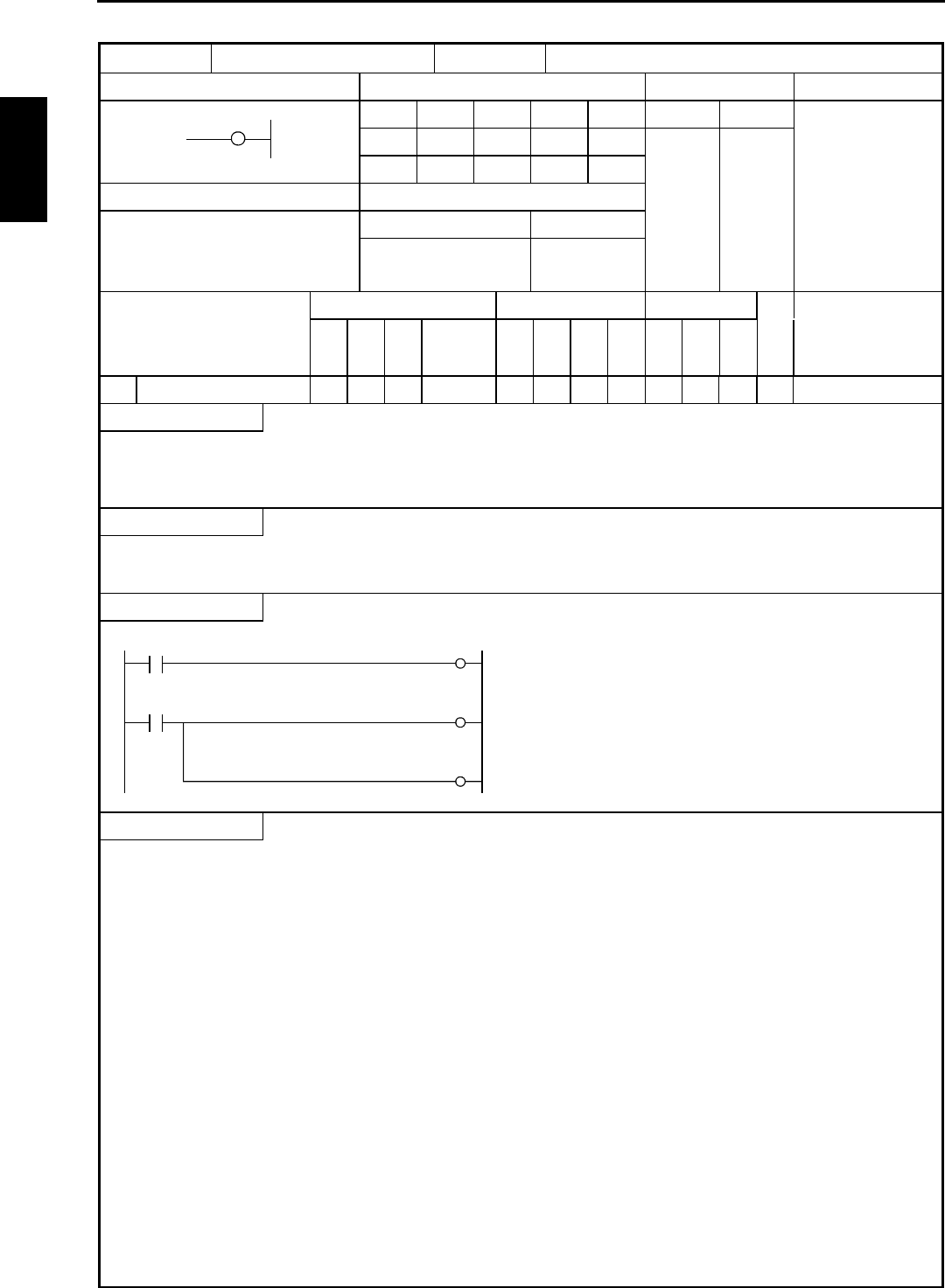
Chapter 5 Instruction Specifications
5-20
Item number Basic instructions-10 Name Coil output (OUT)
Ladder format Condition code Processing time (µs) Remark
R7F4 R7F3 R7F2 R7F1 R7F0 Average Maximum
DER ERR SD V C
zzzzz
Instruction format Number of steps 1.0 ←
Condition Steps
OUT n 1
Bit Word Double word
Usable I/O XY
R,
M
TD, SS,
CU, CT WX WY
WR,
WM TC DX DY
DR,
DM
Constant
Other
n I/O number {{ {
Function
•Switches on the coil when the operation result obtained up to that point is “1.”
•Switches off the coil when the operation result obtained up to that point is “0.”
Notes
•L becomes the internal output when link modules are not used.
Program example
X00000
X00001
Y00100
Y00101
LD
OUT
LD
OUT
OUT
X00000
Y00100
X00001
Y00101
Y00102
Y00102
Program description
•When input X00000 is on, the operation is “1” and Y00100 turns on.
•When input X00001 is on, the operation is “1,” and Y00101 and Y00102 turn on.
n
OUT n
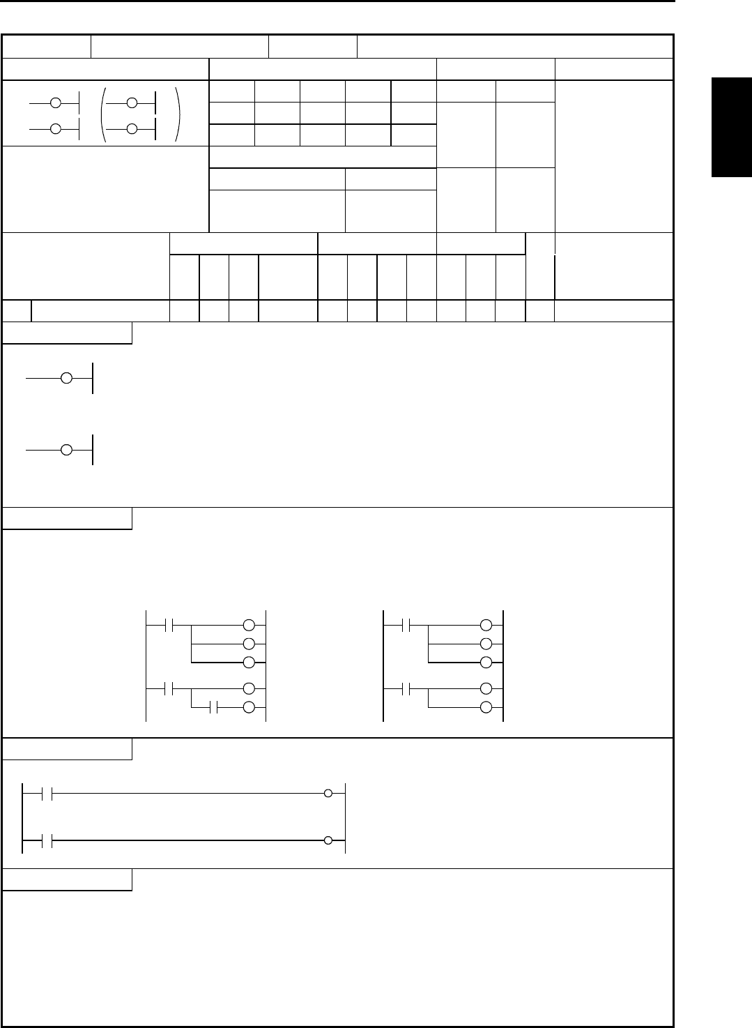
Chapter 5 Instruction Specifications
5-21
Item number Basic instructions-11, 12 Name Set/reset coil output (SET, RES)
Ladder format Condition code Processing time (µs) Remark
R7F4 R7F3 R7F2 R7F1 R7F0 Average Maximum
DER ERR SD V C Upper case: SET
n
SET
n
RES
S
R
n
SET
n
RES zzzzz 0.9 ←Lower case: RES
Instruction format Number of steps
SET n Condition Steps
RES n 10.9
←
Bit Word Double word
Usable I/O XY
R,
M
TD, SS,
CU, CT WX WY
WR,
WM TC DX DY
DR,
DM
Constant
Other
n I/O number {{
Function
n
SET
SET n Switches on the device when the operation result obtained up to that point is “1.”
The device that is switched on will not be switched off even if the operation result is “0.”
n
RES
RES n Switches off the device when the operation result obtained up to that point is “1.”
( ) indicates the display when the Ladder Editor is used.
Notes
•When a set/reset coil is used on a multi-layer coil, it must be set to the highest level or an arbitrary contact must be entered
immediately before the use.
Example of OK Example of NG
SET
SET
SET
SET
SET
Program example
X00000
X00001
R100
R100
LD
SET
LD
RES
X00000
R100
X00001
R100
SET
RES
Program description
•When input X00000 turns on, output R100 turns on. Even if X00000 turns off, R100 remains on.
•When input X00001 turns on, output R100 turns off.
•When input X00000 and X00001 both turn on, the one executed later than the other during programming takes a higher
priority.
SET n
RES n
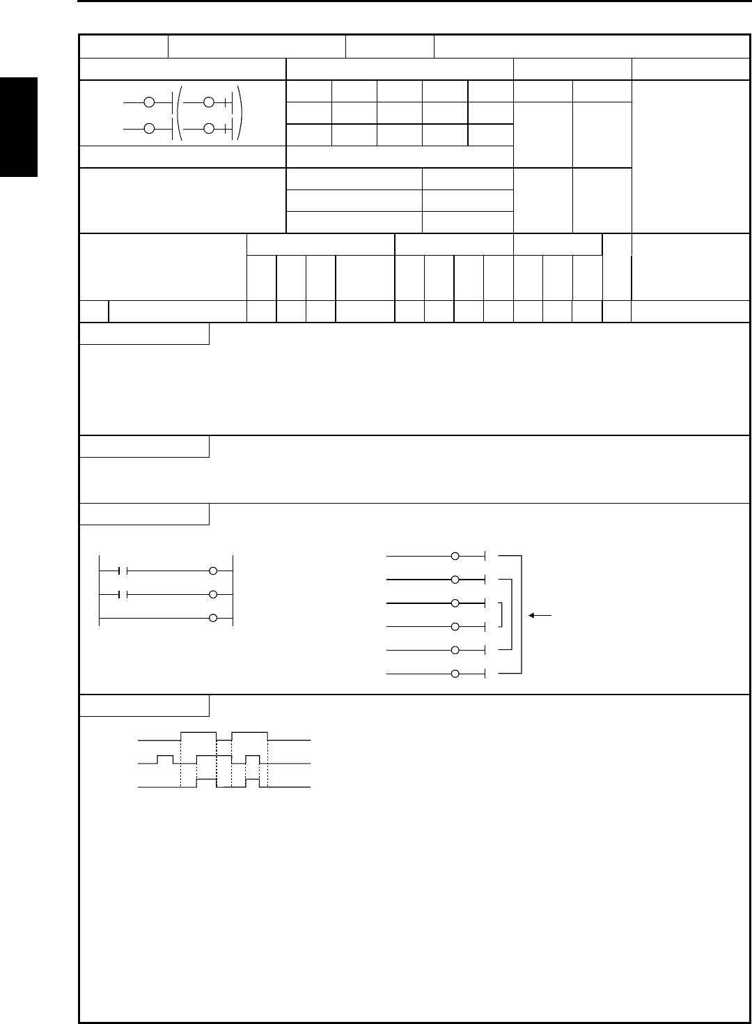
Chapter 5 Instruction Specifications
5-22
Item number Basic instructions-13, 14 Name Set (start)/reset (cancel) master control (MCS, MCR)
Ladder format Condition code Processing time (µs) Remark
R7F4 R7F3 R7F2 R7F1 R7F0 Average Maximum
DER ERR SD V C Upper case: MCS
MCS n
MCR n
S
R
MCS n
MCR n
zzzzz 0.7 ←Lower case: MCR
Instruction format Number of steps
MCS n Condition Steps
MCR n MCS n 3 0.7 ←
MCR n 2
Bit Word Double word
Usable I/O XY
R,
M
TD, SS,
CU, CT WX WY
WR,
WM TC DX DY
DR,
DL,
DM
Constant
Other
n Number {0 to 49 (Decimal)
Function
•Controls the input to the circuit sandwiched by the master control set (MCS n) and reset (MCR n).
(An AND operation is performed with respect to each input and MCS.)
•The master control can be used up to eight layers.
( ) indicates the display when the Ladder Editor is used.
Notes
•Always use the master control MCS and MCR in pairs.
Program example
X00000
X00001
MCS1
Y00100
MCR1
LD X00000
MCS1
LD X00001
OUT Y00100
MCR1
MCS0
MCS1
MCS2
MCR2
MCR1
MCR0
Up to eight layers
are allowed.
Program description
X
00000
X
00001
Y
00100
•When input X00000 is on, the circuits surrounded by MCS and MCR obeys input X00001, and output Y00100 turns on/off.
•When input X00000 is off, the circuits surrounded by MCS and MCR are independent of input X00001, and output Y00100
turns off.
MCS n
MCR n
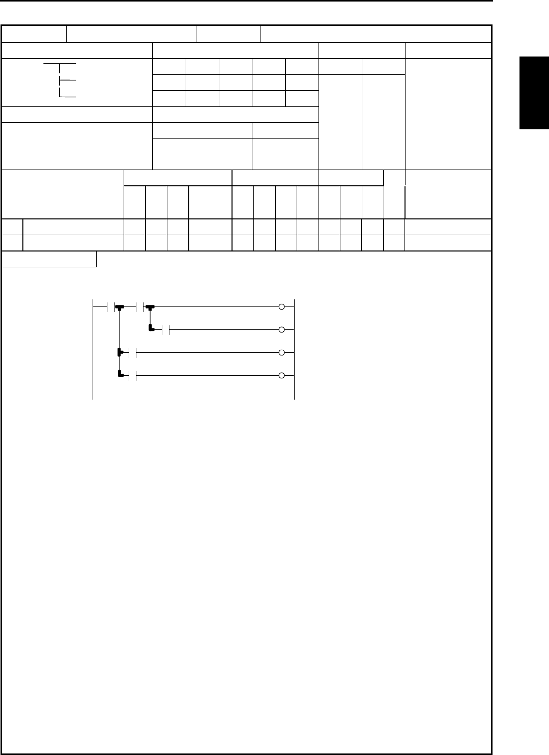
Chapter 5 Instruction Specifications
5-23
Item number Basic instructions-15, 16, 17 Name Save/read/clear operation result (Branching of ladder)
Ladder format Condition code Processing time (µs) Remark
R7F4 R7F3 R7F2 R7F1 R7F0 Average Maximum
DER ERR SD V C
Save
Read
Clear zzzzz
Instruction format Number of steps
MPS Save Condition Steps
MRD Read 0
MPP Clear
Bit Word Double word
Usable I/O XY
R,
M
TD, SS,
CU, CT WX WY
WR,
WM TC DX DY
DR,
DM
Constant
Other
Function
X00100 Y00101
LD X00100
MPS
AND R001
MPS
OUT Y00101
MPP
AND R002
OUT Y00102
MRD
AND R003
OUT Y00103
MPP
AND R004
OUT Y00104
R001
Y00102R002
Y00103R003
Y00104R004
•MPS stores the previous operation result. (Push)
•MRD reads the results stored by the MPS and continues operation.
•MPP reads the results stored previously by the MPS and continues operation, then clears the results after operation. (Pull)
MPS Save
MRD Read
MPP Clear
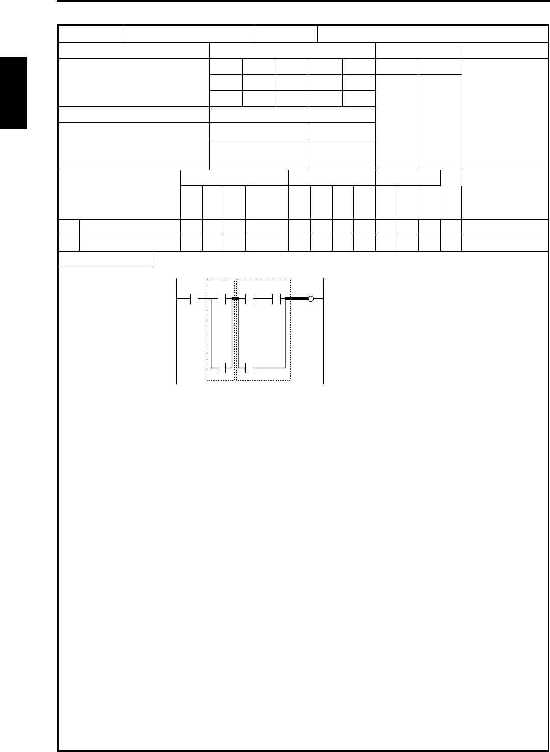
Chapter 5 Instruction Specifications
5-24
Item number Basic instructions-18 Name Logical block serial connection (ANB)
Ladder format Condition code Processing time (µs) Remark
R7F4 R7F3 R7F2 R7F1 R7F0 Average Maximum
(See Function column) DER ERR SD V C
zzzzz
Instruction format Number of steps
Condition Steps
ANB 0
Bit Word Double word
Usable I/O XY
R,
M
TD, SS,
CU, CT WX WY
WR,
WM TC DX DY
DR,
DM
Constant
Other
Function
X00001 Y00100 LD X00001
LD R010
OR R011
ANB
LD M0020
AND M0021
OR M0022
ANB
OUT Y00100
R010 M0020 M0021
R011 M0022
This instruction is used to perform AND operation with respect to the logical operation blocks (dotted line area).
ANB
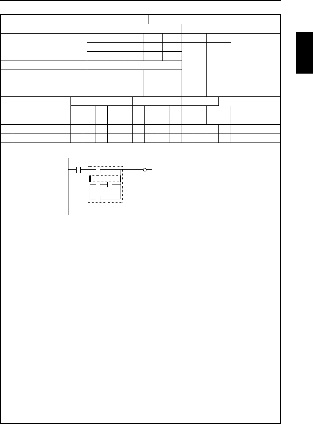
Chapter 5 Instruction Specifications
5-25
Item number Basic instructions-19 Name Logical block parallel connection (ORB)
Ladder format Condition code Processing time (µs) Remark
R7F4 R7F3 R7F2 R7F1 R7F0 Average Maximum
(See Function column) DER ERR SD V C
zzzzz
Instruction format Number of steps 0.7
Condition Steps
ORB 1
Bit Word Double word
Usable I/O XY
R,
M
TD, SS,
CU, CT WX WY
WR,
WM TC DX DY
DR,
DM
Constant
Other
Function
X00000 Y00105 LD X00000
LD R010
LD R011
AND R012
ORB
OR X00001
ANB
OUT Y00105
R010
R011
X00001
R012
This instruction is used to perform OR operation with respect to the logical operation blocks (dotted line area).
ORB

Chapter 5 Instruction Specifications
5-26
Item number Basic instructions-20 Name Processing box start and end (PROCESSING BOX)
Ladder format Condition code Processing time (µs) Remark
R7F4 R7F3 R7F2 R7F1 R7F0 Average Maximum
DER ERR SD V C
zzzzz
Instruction format Number of steps 0.6
Condition Steps
[ ] — 3
Bit Word Double word
Usable I/O XY
R,
M
TD, SS,
CU, CT WX WY
WR,
WM TC DX DY
DR,
DM
Constant
Other
Function
•Indicates the start and end of the processing box.
X00001
WY0010=WX0000
LD X00001
[
WY0010=WX0000
]
•In the above example, the operation inside the processing box will be executed when input X00001 is on.
Parallel connection of processing box or coil is not allowed.
[
]
Not allowed Allowed
Not allowed Allowed
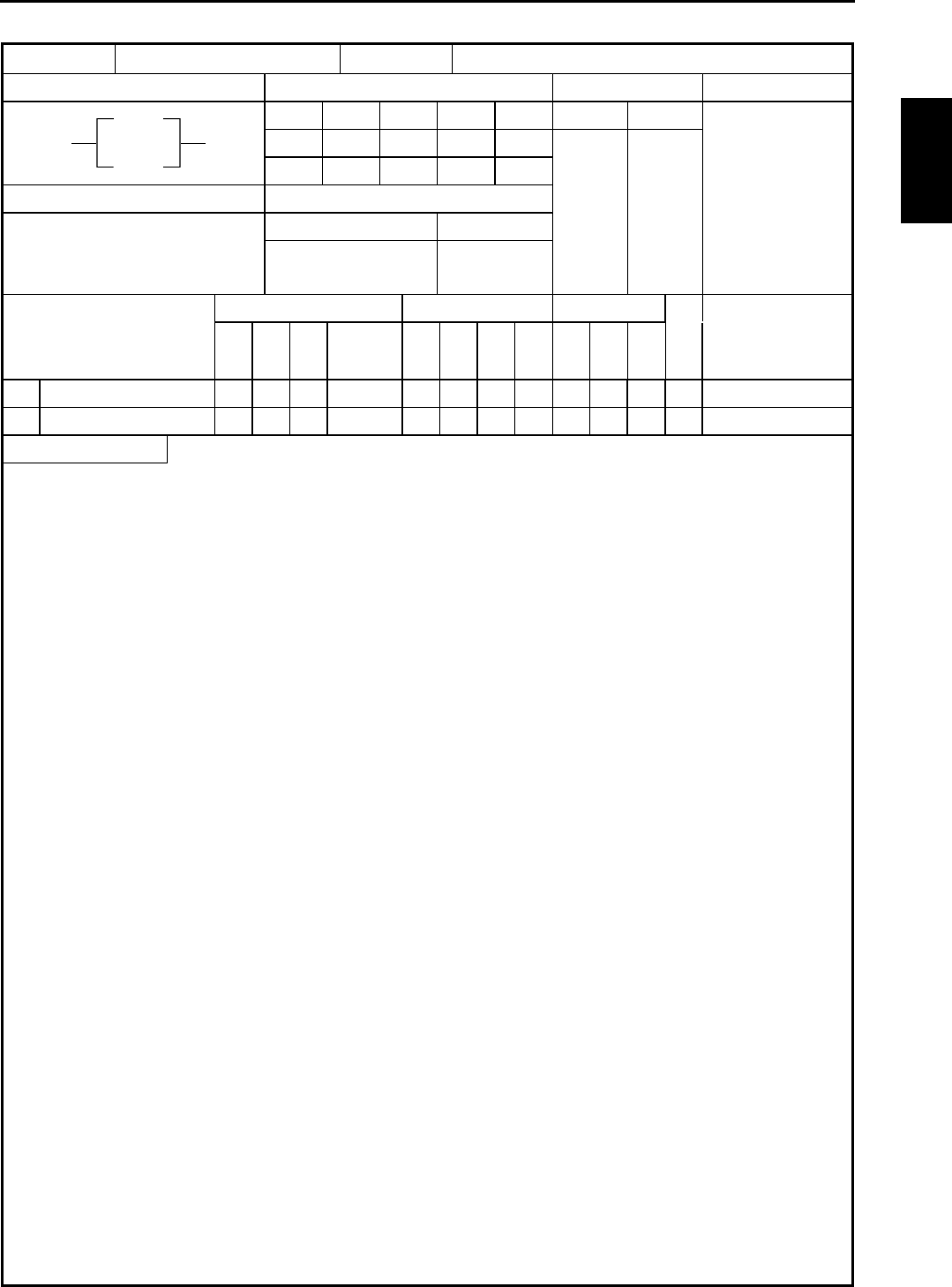
Chapter 5 Instruction Specifications
5-27
Item number Basic instructions-21 Name Relational box start and end (RELATIONAL BOX)
Ladder format Condition code Processing time (µs) Remark
R7F4 R7F3 R7F2 R7F1 R7F0 Average Maximum
DER ERR SD V C
zzzzz
Instruction format Number of steps 0.8
Condition Steps
( ) — 0
Bit Word Double word
Usable I/O XY
R,
M
TD, SS,
CU, CT WX WY
WR,
WM TC DX DY
DR,
DM
Constant
Other
Function
•Indicates the start and end of the relational box.
z
z
( )
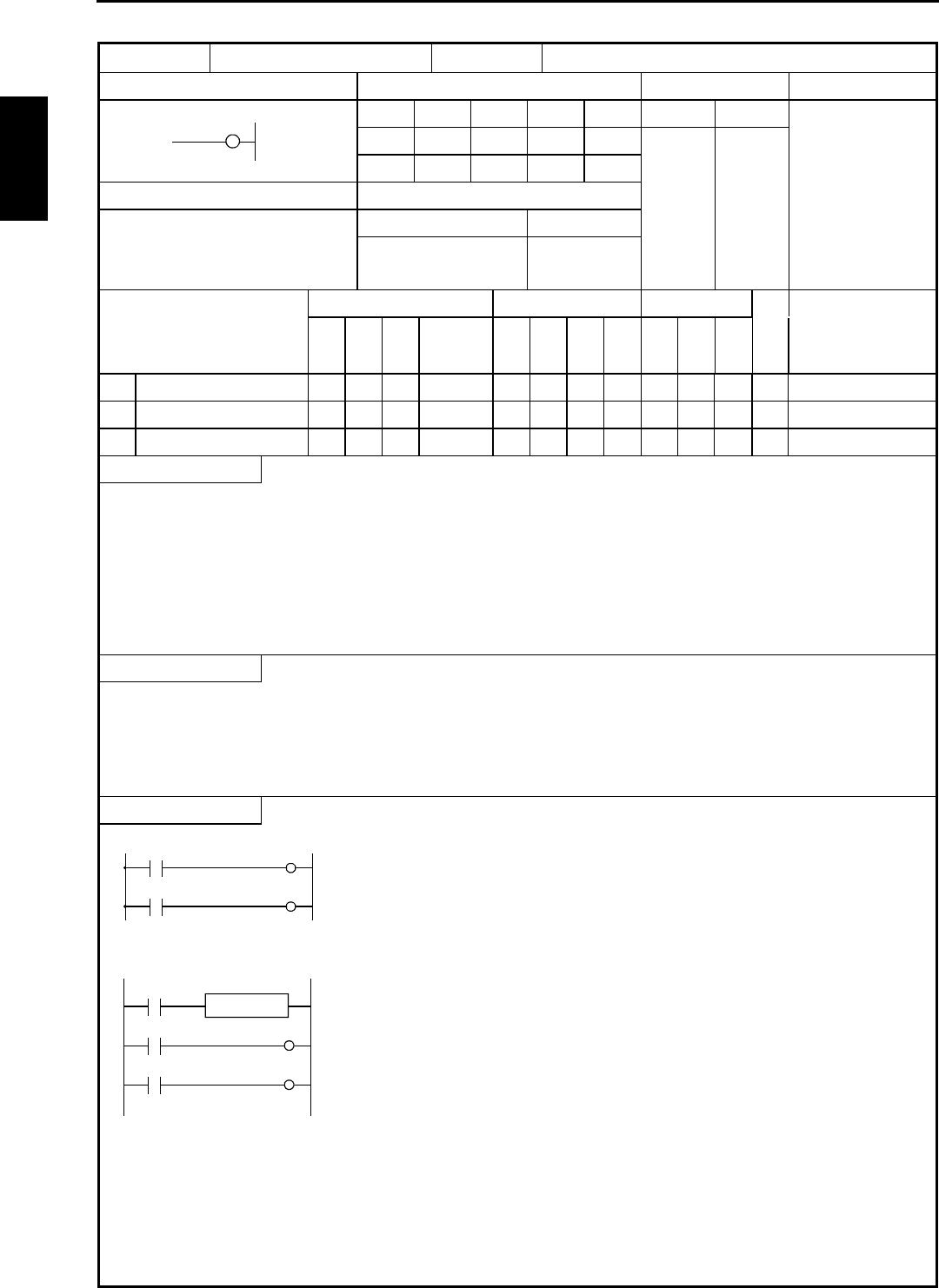
Chapter 5 Instruction Specifications
5-28
Item number Basic instructions-22 Name On delay timer (ON DELAY TIMER)
Ladder format Condition code Processing time (µs) Remark
R7F4 R7F3 R7F2 R7F1 R7F0 Average Maximum
DER ERR SD V C
zzzzz
Instruction format Number of steps 1.4
Condition Steps
OUT TD n t s 5
Bit Word Double word
Usable I/O XY
R,
M
TD, SS,
CU, CT WX WY
WR,
WM TC DX DY
DR,
DM
Constant
Other
n Timer number {0 to 255 (Decimal)
tTime base .01s, .1s, 1s
sSet value {{{ {1 to 65535 (Decimal)
Function
•The progress value is updated when the startup condition is on, and the coil turns on when the progress value is greater than
or equal to the set value.
•If the startup condition is turned off, the progress value is cleared and the coil turns off.
•The progress value is set in TC n and does not exceed 65535 (decimal).
•If the progress value is updated during RUN, the operation will be performed using the new progress value at that point.
•If an I/O is set for the set value, the set value can be changed during operation by changing the I/O value, since the set values
are updated during each scan.
Notes
•The .01s time base can only be used for timer numbers 0 to 63 (64 points).
•The .1 s and 1 s time bases can be used for all timer numbers (0 to 255).
•A maximum of 256 points can be used for the timers TD, SS, CU, CTU and CTD in total.
However, the same area as the counter is used. The timer numbers and counter numbers may not be overlapped.
Program example
X00000 TD10 LD X00000
OUT TD10 0.01S 12345
LD TD10
OUT R100
TD10 R100
0.01S 12345
•An example of a word I/O being used as the set value for the circuit shown above.
R7E3
X00000 TD10
0.01S WR0010
TD10 R100
WR0010=12345
LD R7E3
[
WR0010=12345
]
LD X00000
OUT TD10 0.01S WR0010
LD TD10
OUT R100
TD n
t x s
OUT TD n t s

Chapter 5 Instruction Specifications
5-29
Program description
[Time chart]
X00000
12345
65 535
TD10
R100
Progress value
of TD10 (TC10)
1] 2] 3] 4] 5]
Set value
1] When input X00000 turns on, TD progress value is updated.
2] When input X00000 turns off, the TD progress value is cleared.
3] TD10 turns on when progress value ≥ set value.
4] While X00000 is on, the progress value increases, but will not
increase exceeding 65535.
5] When X00000 turns off, TD10 also turns off and the progress value
is cleared.
•Example using word I/O as the set value
When RUN is commenced, the set value is set to the word I/O.
Or, the word I/O for the set value is designated to store in the power failure memory.
OUT TD n t s

Chapter 5 Instruction Specifications
5-30
Item number Basic instructions-23 Name Single shot (SINGLE SHOT)
Ladder format Condition code Processing time (µs) Remark
R7F4 R7F3 R7F2 R7F1 R7F0 Average Maximum
DER ERR SD V C
zzzzz
Instruction format Number of steps 1.4
Condition Steps
OUT SS n t s 5
Bit Word Double word
Usable I/O
XY
R,
M
TD, SS,
WDT, MS,
TMR, CU,
RCU, CT WX WY
WR,
WM TC DX DY
DR,
DM
Constant
Other
n Timer number {0 to 255 (Decimal)
tTime base .01s, .1s, 1s
sSet value {{{ {1 to 65535 (Decimal)
Function
•Detects the leading edge of the startup condition, starts updating progress values, and turns on the coil.
•The coils turns off when the progress value is greater than or equal to the set value. If a leading edge is detected while the
progress value is less than the set value, the progress value is set to 0 and the counter is reset.
•The progress value is set in TC n and does not exceed 65535 (decimal).
•If the progress value is updated during RUN, the operation will be performed using the new progress value at that point.
•If an I/O is set for the set value, the set value can be changed during operation by changing the I/O value, since the set values
are updated during each scan.
Notes
•The .01 s time base can only be used for timer numbers 0 to 63 (64 points).
•The .1 s and 1s time bases can be used for all timer numbers (0 to 255).
•A maximum of 256 points can be used for the timers TD, SS, CU, CTU and CTD in total.
However, the same area as the counter is used. Timer number and counter number may not be overlapped.
•Since the startup condition of a single shot is edge detection, the condition for one scan cannot be detected during the first
scan after RUN starts.
Program example
X00001 SS11 LD X00001
OUT SS11 0.01S 12567
LD SS11
OUT R101
SS11 R101
0.01S 12567
•An example of a word I/O being used as the set value for the circuit shown above.
R7E3
X00001 SS11
0.01S WR0011
SS11 R101
WR0011=12567
LD R7E3
[
WR0011=12567
]
LD X00001
OUT SS11 0.01S WR0011
LD SS11
OUT R101
SS n
t x s
OUT SS n t s

Chapter 5 Instruction Specifications
5-31
Program description
[Time chart]
X00001
SS11
R101
12 567
Progress
value of SS11
(TC11) 1] 2] 3] 4]
Set value
1] The progress value is updated and SS11 turns on at the leading edge
of X00001.
2] SS11 turns off when set value ≥ progress value.
X00001 is turned on at this time, but the single shot startup
conditions are ignored because it uses edge trigger.
3] SS11 is turned on at the leading edge of X00001 again, and the
progress value is updated.
4] When the leading edge of X00001 is detected while the progress
value does not reach the set value, the single shot timer is triggered
again and the progress value returns to 0, then starts increasing. The
SS11 remains on.
•Example using word I/O as the set value
When RUN is commenced, the set value is set to the word I/O.
Or, the word I/O for the set value is designated to store in the power failure memory.
OUT SS n t s

Chapter 5 Instruction Specifications
5-32
Item number Basic instructions-24 Name Counter (COUNTER)
Ladder format Condition code Processing time (µs) Remark
R7F4 R7F3 R7F2 R7F1 R7F0 Average Maximum
DER ERR SD V C
CU n
s
zzzzz
Instruction format Number of steps 1.4
Condition Steps
OUT CU n s — 5
Bit Word Double word
Usable I/O XY
R,
M
TD, SS,
CU, CT WX WY
WR,
WM TC DX DY
DR,
DM
Constant
Other
n Counter number {0 to 255 (Decimal)
sSet value {{{ {1 to 65535 (Decimal)
Function
•Increments the progress value by 1 each time the leading edge of the startup condition is detected, and switches on the coil
when the progress value is greater than or equal to the set value. The coil that is switched on turns off when the counter
clear CL n is switched on, and the progress value is cleared to 0.
•The progress value is set in TC n and does not exceed 65535 (decimal).
•If the progress value is updated while the system is running, the operation will be performed using the new progress value at
that point.
•If an I/O is set for the set value, the set value can be changed during operation by changing the I/O value, since the set values
are updated during each scan.
Notes
•A maximum of 256 points can be used for the timers and counters TD, SS, CU, CTU and CTD in total.
•The timer numbers and counter numbers can not be overlapped.
•While the counter clear CL n is on, the rise of startup condition is ignored.
•Since the startup condition of the counter is edge detection, the condition for one scan can not be detected during the first
scan after RUN starts.
•If the set value is set to 0, it is regarded as a coil that is always on and controlled by the CL n.
Program example
X00005 CU15
LD X00005
OUT CU15 4
LD X00006
OUT CL15
LD CU15
OUT R105
X00006 CL15
4
CU15 R105
•An example of a word I/O being used as the set value for the circuit shown above.
R7E3
X00005 CU15
WR0015
X00006 CL15
WR0015=4
LD R7E3
[
WR0015=4
]
LD X00005
OUT CU15 WR0015
LD X00006
OUT CL15
LD CU15
OUT R105
CU15 R105
OUT CU n s
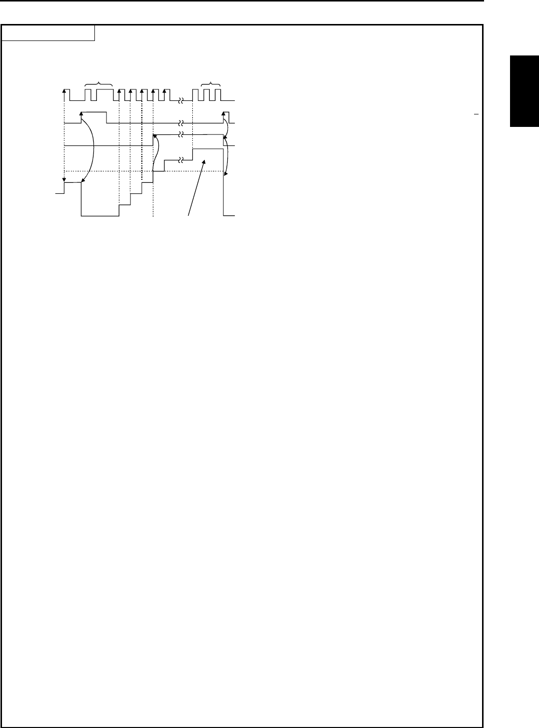
Chapter 5 Instruction Specifications
5-33
Program description
[Time chart]
X00005
CL15
CU15
1
2
3
4
5
65 535
3
Progress
value of
CU15 (TC15)
1] 2] 4]
Set value 4
5]
3]
Ignored Ignored
1] The progress value (count) is cleared to 0 by the counter
clear (CL15). While the counter clear is on, the progress
value will not be updated.
2] The progress value is updated at the leading edge of
X00005.
3] Counter coil (CU15) is turned on since the progress value ≥
set value.
4] The count value will not exceed 65535 (decimal).
5] The progress value and counter coil are cleared by counter
clear (CL15).
•The clear is performed under the conditions set immediately
prior to the execution of the counter coil instruction.
•Example using word I/O as the set value
When RUN is commenced, the set value is set to the word I/O.
Or, the word I/O for the set value is designated to store in the power failure memory.
OUT CU n s

Chapter 5 Instruction Specifications
5-34
Item number Basic instructions-25, 26 Name Up (CTU n) and down (CTD n) of up/down counter
(UP/DOWN COUNTER)
Ladder format Condition code Processing time (µs) Remark
R7F4 R7F3 R7F2 R7F1 R7F0 Average Maximum
DER ERR SD V C Upper case: CTU
CTD n
CTU n s
zzzzz 1.4 Lower case: CTD
Instruction format Number of steps
OUT CTU n s Condition Steps
OUT CTD n CTU 5 1.4
CTD 3
Bit Word Double word
Usable I/O XY
R,
M
TD, SS,
CU, CT WX WY
WR,
WM TC DX DY
DR,
DM
Constant
Other
n Counter number {0 to 255 (Decimal)
sSet value {{{ {1 to 65535 (Decimal)
Function
•For the UP counter, increments the progress value by 1 each time the leading edge of the startup condition is detected, while
it decrements the progress value by 1 for the DOWN counter. The coil switches on when the progress value is greater than
or equal to the set value and switches off when the progress value is less than the set value. When the counter clear CL n
switches on, the progress value is cleared to 0 and the coil switches off.
•The progress value is set in TC n, and the value will be in the range of 0 to 65535 (decimal).
•If the progress value is updated during RUN, the operation will be performed using the new progress value at that point.
•If an I/O is set for the set value, the set value can be changed during operation by changing the I/O value, since the set values
are updated during each scan.
Notes
•A maximum of 256 points can be used for the timers and counters TD, SS, CU, CTU and CTD in total.
•The timer numbers and counter numbers cannot be overlapped.
•The numbers for the UP coil and DOWN coil must be the same.
•While the counter clear CL n is on, the rise of startup condition is ignored.
•Since the startup condition of the counter is edge detection, the condition for one scan may not be detected during the first
scan after RUN starts.
•If the set value is set to “0”, it is regarded as a coil that is always on and controlled by the CL n.
OUT CTU n s
OUT CTD n
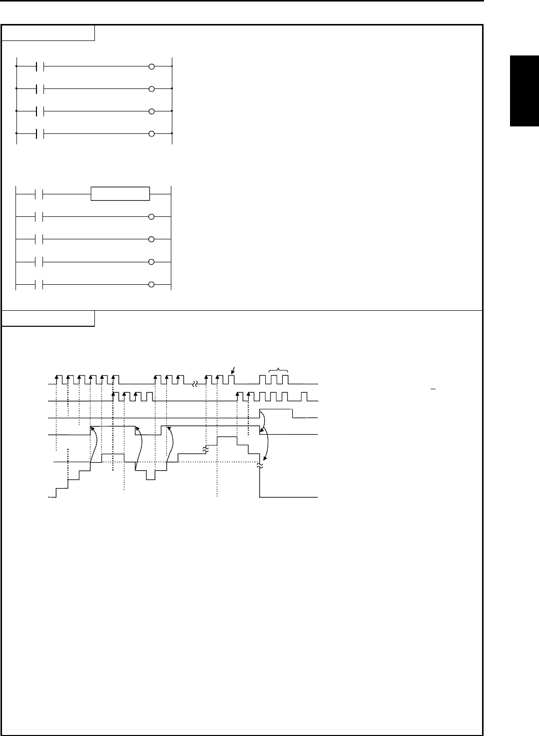
Chapter 5 Instruction Specifications
5-35
Program example
X00007 CTU17
LD X00007
OUT CTU17 4
LD X00008
OUT CTD17
LD X00009
OUT CL17
LD CT17
OUT R107
X00008 CTD17
4
X00009 CL17
CT17 R107
•An example of a word I/O being used as the set value for the circuit shown above.
R7E3
X00007 CTU17
WR0017
X00008 CTD17
WR0017=4
LD R7E3
[
WR0017=4
]
LD X00007
OUT CTU17 WR0017
LD X00008
OUT CTD17
LD X00009
OUT CL17
LD CT17
OUT R107
X00009 CL17
CT17 R107
Program description
[Time chart]
1
2
3
4
5
4
3
2
3
4
5
65 535
65 534
0
X00007
X00008
CL17
CT17
=4
Ignored
1] 2] 4] 5]
3] 7]
6] 6]
Set value
Progress value
(TC17)
Ignored
Ignored
1] The progress value (count value) is
up-counted at the leading edge of
X00007.
2] The counter coil (CT17) is turned on
when the progress value ≥ set value.
3] When the up-coil and down-coil
startup conditions turn on
simultaneously, the progress value
does not change.
4] The progress value is down-counted
at the leading edge of X00008.
5] The counter coil turns off when set
value > progress value.
6] The progress value will not exceed 65535 (decimal). Also, it will not be below 0.
7] When the counter clear (CL17) turns on, the progress value and the counter coil are cleared. The progress value is not
updated while the counter clear is on.
•The clear is performed under the conditions set immediately before execution of the counter coil instruction.
•Example using the word I/O as the set value
When RUN is commenced, the set value is set to word I/O.
Or, the word I/O for the set value is designated to store in the power failure memory.
z
OUT CTU n s
OUT CTD n

Chapter 5 Instruction Specifications
5-36
Item number Basic instructions-27 Name Counter clear (COUNTER CLEAR)
Ladder format Condition code Processing time (µs) Remark
R7F4 R7F3 R7F2 R7F1 R7F0 Average Maximum
DER ERR SD V C
CL n
zzzzz
Instruction format Number of steps 0.9
Condition Steps
OUT CL n s — 1
Bit Word Double word
Usable I/O XY
R,
M
TD, SS,
CU, CT WX WY
WR,
WM TC DX DY
DR,
DM
Constant
Other
n Counter number {0 to 255 (Decimal)
Function
•Clears the progress values of the integral timer and switches off the timer coil.
•In the case of WDT, the time monitor check is performed (see WDT for details).
•In the case of counters, the progress value is cleared and the counter coil is switched off.
•The clearing operation is conducted immediately before execution of the counter or timer coil instruction indicated by the
clear coil.
Example:
X00000 CL10
X00001 CU10
X00002 CL10
1) When X00000 is turned on, the CL10 immediately prior to CU10, and CU10
is cleared.
2) Even if X00002 turns on, if X00001 is off, the CL10 is turned off by the
circuit before CU10 is executed. Thus, the CU10 will not be cleared.
Notes
•The same number should be used for the timer number and counter number.
OUT CL n s

Chapter 5 Instruction Specifications
5-37
Item number Basic instructions-28 Name =Relational box (=RELATIONAL BOX)
Ladder format Condition code Processing time (µs) Remark
R7F4 R7F3 R7F2 R7F1 R7F0 Average Maximum
(See Function column) DER ERR SD V C Upper case: W
zzzzz 27 40 Lower case: DW
Instruction format Number of steps
LD (s1 == s2) Condition Steps
AND (s1 == s2) Word (See Notes) 35 50
OR (s1 == s2) Double word (See Notes)
Bit Word Double word
Usable I/O XY
R,
M
TD, SS,
CU, CT WX WY
WR,
WM TC DX DY
DR,
DM
Constant
Other
s1 Relational number 1 {{{{{{{{
s2 Relational number 2 {{{{{{{{
Function
[Ladder format] s1
==
s2
s1
==
s2
s1
==
s2
•Compares s1 and s2 as unsigned numbers, and
if s1 is equals to s2, it enters the continuity status (on) and
if s1 is not equal to s2, enters the noncontinuity status (off).
•When s1 and s2 are words: 0 to 65535 (decimal) or H0000 to HFFFF (hexadecimal)
When s1 and s2 are double words: 0 to 4294967295 (decimal) or H00000000 to HFFFFFFFF (hexadecimal)
Notes
[Number of steps]
Word Double word LD, AND (s1==s2) OR (s1==s2)
LD (s1 == s2) 5 steps I/O I/O 5 steps 6 steps
AND (s1 == s2) 5 steps I/O Constant 6 steps 7 steps
OR (s1 == s2) 6 steps Constant I/O 6 steps 7 steps
Constant Constant 7 steps 8 steps
Program example
R001
WR0000
= =
WR0002
LD (WR0000 == WR0002)
OUT R001
Program description
•When WR0000 = WR0002, R001 turns on.
LD (s1 == s2)
AND (s1 == s2)
OR (s1 == s2)

Chapter 5 Instruction Specifications
5-38
Item number Basic instructions-29 Name Signed = Relational box (SIGNED = RELATIONAL BOX)
Ladder format Condition code Processing time (µs) Remark
R7F4 R7F3 R7F2 R7F1 R7F0 Average Maximum
(See Function column) DER ERR SD V C
zzzzz
Command format Number of steps 35 50
LD (s1 S== s2) Condition Steps
AND (s1 S== s2) Double word (See Cautionary notes)
OR (s1 S== s2)
Bit Word Double word
Usable I/O XY
R,
L,
M
TD, SS,
CU, CT WX WY
WR,
WM TC DX DY
DR,
DM
Constant
Other
s1 Relational number 1 {{{{
s2 Relational number 2 {{{{
Function
[Ladder format] s1
S==
s2
s1
S==
s2
s1
S==
s2
z Compares s1 and s2 as signed double-word numbers, and
if s1 is equals to s2, it enters the continuity status (on) and
if s1 is not equal to s2, enters the noncontinuity status(off).
z s1, s2 – 2147483648 to + 2147483647 (decimal)
H80000000 to H7FFFFFFF (hexadecimal)
b31 b0
Sign bit: 0 - Positive; 1 - Negative
Cautionary notes
[Number of steps]
Double word LD, AND (s1S==s2) OR (s1S==s2)
I/O I/O 5 steps 6 steps
I/O Constant 6 steps 7 steps
Constant I/O 6 steps 7 steps
Constant Constant 7 steps 8 steps
Program example
R002
DR0000
S = =
DR0002
LD (DR0000 S== DR0002)
OUT R002
Program description
z When DR0000 = DR0002, R002 turns on (signed).
LD (s1 == s2)
AND (s1 == s2)
OR
(
s1 == s2
)
Chapter 5 Instruction Specifications
5-39
Item number Basic instructions-30 Name <> Relational box (<> RELATIONAL BOX)
Ladder format Condition code Processing time (µs) Remark
R7F4 R7F3 R7F2 R7F1 R7F0 Average Maximum
(See Function column) DER ERR SD V C Upper case: W
zzzzz26.8 40 Lower case: DW
Instruction format Number of steps
LD (s1 <> s2) Condition Steps
AND (s1 <> s2) Word (See Notes) 34.5 50
OR (s1 <> s2) Double word (See Notes)
Bit Word Double word
Usable I/O XY
R,
M
TD, SS,
CU, CT WX WY
WR,
WM TC DX DY
DR,
DM
Constant
Other
s1 Relational number 1 {{{{{{{{
s2 Relational number 2 {{{{{{{{
Function
[Ladder format] s1
<>
s2
s1
<>
s2
s1
<>
s2
•Compares s1 and s2 as unsigned numbers, and
if s1 is equals to s2, it enters the noncontinuity status (off) and
if s1 is not equal to s2, enters the continuity status (on).
•When s1 and s2 are words: 0 to 65535 (decimal) or H0000 to HFFFF (hexadecimal)
When s1 and s2 are double words: 0 to 4294967295 (decimal) or H00000000 to HFFFFFFFF (hexadecimal)
Notes
[Number of steps]
Word Double word LD, AND (s1<>s2) OR (s1<>s2)
LD (s1 <> s2) 5 steps I/O I/O 5 steps 6 steps
AND (s1 <> s2) 5 steps I/O Constant 6 steps 7 steps
OR (s1 <> s2) 6 steps Constant I/O 6 steps 7 steps
Constant Constant 7 steps 8 steps
Program example
R003
WR0000
< >
WR0002
LD (WR0000 < > WR0002)
OUT R003
Program description
•When WR0000 ≠ WR0002, R003 turns on.
LD (s1 <> s2)
AND (s1 <> s2)
OR (s1 <> s2)

Chapter 5 Instruction Specifications
5-40
Item number Basic instructions-31 Name Signed <> Relational box (SIGNED <> RELATIONAL
BOX)
Ladder format Condition code Processing time (µs) Remark
R7F4 R7F3 R7F2 R7F1 R7F0 Average Maximum
(See Function column) DER ERR SD V C
zzzzz
Command format Number of steps 34.5 50
LD (s1 S<> s2) Condition Steps
AND (s1 S<> s2) Double word (See Cautionary notes)
OR (s1 S<> s2)
Bit Word Double word
Usable I/O XY
R,
L,
M
TD, SS,
CU, CT WX WY
WR,
WM TC DX DY
DR,
DM
Constant
Other
s1 Relational number 1 {{{{
s2 Relational number 2 {{{{
Function
[Ladder format] s1
S<>
s2
s1
s2
s1
s2
S<> S<>
z Compares s1 and s2 as signed double-word numbers, and
if s1 is equals to s2, it enters the noncontinuity status (off) and
if s1 is not equal to s2, enters the continuity status (on).
z s1, s2 – 2147483648 to + 2147483647 (decimal)
H80000000 to H7FFFFFFF (hexadecimal)
b31 b0
Sign bit: 0 - Positive; 1 - Negative
Cautionary notes
[Number of steps]
Double word LD, AND (s1S<>s2) OR (s1S<>s2)
I/O I/O 5 steps 6 steps
I/O Constant 6 steps 7 steps
Constant I/O 6 steps 7 steps
Constant Constant 7 steps 8 steps
Program example
R004
DR0000
S < >
DR0002
LD (DR0000 S < > DR0002)
OUT R004
Program description
z When DR0000 ≠ DR0002, R004 turns on (signed).
LD (s1 S <> s2)
AND (s1 S <> s2)
OR
(
s1 S <> s2
)

Chapter 5 Instruction Specifications
5-41
Item number Basic instructions-32 Name <Relational box (<RELATIONAL BOX)
Ladder format Condition code Processing time (µs) Remark
R7F4 R7F3 R7F2 R7F1 R7F0 Average Maximum
(See Function column) DER ERR SD V C Upper case: W
zzzzz26.8 40 Lower case: DW
Instruction format Number of steps
LD (s1 < s2) Condition Steps
AND (s1 < s2) Word (See Notes) 37.5 52
OR (s1 < s2) Double word (See Notes)
Bit Word Double word
Usable I/O XY
R,
M
TD, SS,
CU, CT WX WY
WR,
WM TC DX DY
DR,
DM
Constant
Other
s1 Relational number 1 {{{{{{{{
s2 Relational number 2 {{{{{{{{
Function
[Ladder format] s1
<
s2
s1
<
s2
s1
<
s2
•Compares s1 and s2 as unsigned numbers, and
if s1 is less than s2, it enters the continuity status (on) and
if s1 is greater than or equal to s2, enters the noncontinuity status (off).
•When s1 and s2 are words: 0 to 65535 (decimal) or H0000 to HFFFF (hexadecimal)
When s1 and s2 are double words: 0 to 4294967295 (decimal) or H00000000 to HFFFFFFFF (hexadecimal)
Notes
[Number of steps]
Word Double word LD, AND (s1<s2) OR (s1<s2)
LD (s1 < s2) 5 steps I/O I/O 5 steps 6 steps
AND (s1 < s2) 5 steps I/O Constant 6 steps 7 steps
OR (s1 < s2) 6 steps Constant I/O 6 steps 7 steps
Constant Constant 7 steps 8 steps
Program example
R005
WR0000
<
WR0002
LD (WR0000 < WR0002)
OUT R007
Program description
•When WR0000 < WR0002, R005 turns on.
LD (s1 < s2)
AND (s1 < s2)
OR (s1 < s2)

Chapter 5 Instruction Specifications
5-42
Item number Basic instructions-33 Name Signed<Relational box (SIGNED < RELATIONAL BOX)
Ladder format Condition code Processing time (µs) Remark
R7F4 R7F3 R7F2 R7F1 R7F0 Average Maximum
(See Function column) DER ERR SD V C
zzzzz
Command format Number of steps 37.5 53
LD (s1 S< s2) Condition Steps
AND (s1 S< s2) Double word (See Cautionary notes)
OR (s1 S< s2)
Bit Word Double word
Usable I/O XY
R,
L,
M
TD, SS,
CU, CT WX WY
WR,
WM TC DX DY
DR,
DM
Constant
Other
s1 Relational number 1 {{{{
s2 Relational number 2 {{{{
Function
[Ladder format] s1
S<
s2
s1
s2
s1
s2
S< S<
z Compares s1 and s2 as signed double-word numbers, and
if s1 is less than s2, it enters the continuity status (on) and
if s1 is greater than or equal to s2, enters the noncontinuity status
(off).
z s1, s2 – 2147483648 to + 2147483647 (decimal)
H80000000 to H7FFFFFFF (hexadecimal)
b
31 b0
Sign bit: 0 - Positive; 1 - Negative
Cautionary notes
[Number of steps]
Double word LD, AND (s1S<s2) OR (s1S<s2)
I/O I/O 5 steps 6 steps
I/O Constant 6 steps 7 steps
Constant I/O 6 steps 7 steps
Constant Constant 7 steps 8 steps
Program example
R006
DR0000
S <
DR0002
LD (DR0000 S< DR0002)
OUT R006
Program description
z When DR0000 < DR0002, R006 turns on (signed).
LD (s1 S < s2)
AND (s1 S < s2)
OR
(
s1 S < s2
)
Chapter 5 Instruction Specifications
5-43
Item number Basic instructions-34 Name ≤ Relational box (≤ RELATIONAL BOX)
Ladder format Condition code Processing time (µs) Remark
R7F4 R7F3 R7F2 R7F1 R7F0 Average Maximum
(See Function column) DER ERR SD V C Upper case: W
zzzzz26.8 40 Lower case: DW
Instruction format Number of steps
LD (s1 <= s2) Condition Steps
AND (s1 <= s2) Word (See Notes) 42 52
OR (s1 <= s2) Double word (See Notes)
Bit Word Double word
Usable I/O XY
R,
M
TD, SS,
CU, CT WX WY
WR,
WM TC DX DY
DR,
DM
Constant
Other
s1 Relational number 1 {{{{{{{{
s2 Relational number 2 {{{{{{{{
Function
[Ladder format] s1
<=
s2
s1
<=
s2
s1
<=
s2
•Compares s1 and s2 as unsigned numbers, and
if s1 is less than or equal to s2, it enters the continuity status (on) and
if s1 is greater than s2, it enters the noncontinuity status (off).
•When s1 and s2 are words: 0 to 65535 (decimal) or H0000 to HFFFF (hexadecimal)
When s1 and s2 are double words: 0 to 4294967295 (decimal) or H00000000 to HFFFFFFFF (hexadecimal)
Notes
[Number of steps]
Word Double word LD, AND (s1<=s2) OR (s1<=s2)
LD (s1 <= s2) 5 steps I/O I/O 5 steps 6 steps
AND (s1 <= s2) 5 steps I/O Constant 6 steps 7 steps
OR (s1 <= s2) 6 steps Constant I/O 6 steps 7 steps
Constant Constant 7 steps 8 steps
Program example
R007
WR0000
< =
WR0002
LD (WR0000 <= WR0002)
OUT R007
Program description
•When WR0000 ≤ WR0002, R007 turns on.
LD (s1 <= s2)
A
ND (s1 <= s2)
OR (s1 <= s2)
Chapter 5 Instruction Specifications
5-44
Item number Basic instructions-35 Name Signed ≤ Relational box (SIGNED ≤ RELATINAL BOX)
Ladder format Condition code Processing time (µs) Remark
R7F4 R7F3 R7F2 R7F1 R7F0 Average Maximum
(See Function column) DER ERR SD V C
zzzzz
Command format Number of steps 37.5 53
LD (s1 S<= s2) Condition Steps
AND (s1 S<= s2) Double word (See Cautionary notes)
OR (s1 S<= s2)
Bit Word Double word
Usable I/O XY
R,
L,
M
TD, SS,
WDT, MS,
TMR, CU,
RCU, CT
WX WY
WR,
WL,
WM
TC DX DY
DR,
DL,
DM
Constant
Other
s1 Relational number 1 {{{{
s2 Relational number 2 {{{{
Function
[Ladder format] s1
S<=
s2
s1
S<=
s2
s1
S<=
s2
z Compares s1 and s2 as signed double-word numbers, and
if s1 is less than or equal to s2, it enters the continuity status (on) and
if s1 is greater than s2, it enters the noncontinuity status (off).
z s1, s2 – 2147483648 to + 2147483647 (decimal)
H80000000 to H7FFFFFFF (hexadecimal)
b31 b0
Sign bit: 0 - Positive; 1 - Negative
Cautionary notes
[Number of steps]
Double word LD, AND (s1S<=s2) OR (s1S<=s2)
I/O I/O 5 steps 6 steps
I/O Constant 6 steps 7 steps
Constant I/O 6 steps 7 steps
Constant Constant 7 steps 8 steps
Program example
R008
DR0000
S < =
DR0002
LD (DR0000 S<= DR0002)
OUT R008
Program description
z When DR0000 ≤ DR0002, R008 turns on (signed).
LD (s1 S <= s2)
AND (s1 S <= s2)
OR
(
s1 S <= s2
)
Chapter 5 Instruction Specifications
5-45
Item number Arithmetic instructions-1 Name Substitution statement (ASSIGNMENT STATEMENT)
Ladder format Condition code Processing time (µs) Remark
R7F4 R7F3 R7F2 R7F1 R7F0 Average Maximum
d = s DER ERR SD V C
↕zzzz
Instruction format Number of steps (See following table)
Condition Steps
d = s (See Notes)
Bit Word Double word
Usable I/O XY
R,
M
TD, SS,
CU, CT WX WY
WR,
WM TC DX DY
DR,
DM
Constant
Other
d Substitution destination {{ {{{ {{
s Substitution source {{{ {{{{{{{{
( ) Index value {{{
Function
•Substitutes the content of s into d.
•It is possible to use array variables for d and s.
•When d is a word, the constant is 0 to 65535 or – 32768 to + 32767 (decimal)
H0000 to HFFFF or H8000 to H7FFF (hexadecimal)
When d is a double word, the constant is 0 to 4294967295 or -2147483648 to +2147483647 (decimal)
H00000000 to HFFFFFFFF or H80000000 to H7FFFFFFF
Notes
•When using an array variable, DER is set to 1 if the usable I/O number exceeds the maximum value, and DER is reset to “0”
if it is normal.
•The combinations of d and s are as follows:
ds
Bit Bit
Word Word
Double word Double word
•Step numbers and processing time are as follows:
Processing time (µs)
d s Number of steps ( ) indicates DW Bit Word Double word
I/O I/O 3 (4) 32 27 35
I/O Array 4 74 66 86
Array I/O 4 (5) 52 53 71
Array Array 5 92 99 120
d = s

Chapter 5 Instruction Specifications
5-46
Program example
X00000 DIF0
X00001 DIF1
X00002 DIF2
X00003 DIF3
WR0000
WR0000(WM000)=WX0000
WR0000
=WX0000
WR0000(WM000)=WR0000(WM001)
=WR0000(WM001)
Array variables are used at the
substitution destination
Array variables are used at the
substitution source
Array variables are used at both
substitution destination and source
1]
2]
3]
4]
Program description
1] The value of WX0000 is substituted into WR0000 at the leading edge of input X00000.
2] The value of WX0000 is substituted into the WR number designated by WR0000 + WM000 at the leading edge of input
X00001.
1) When WM000 = H0010, it holds the same meaning as WR0010 = WX0000.
3] The word number of the I/O advanced by the amount designated by WR0000 + WM001 due to the I/O assignment is
substituted into WR0000 at the leading edge of input X00002.
1) When WM001 = H0010, it hods the same meaning as WR0000 = WR0010.
4] The I/O value designated by WR0000 + WM001 at the leading edge of input X00003 is substituted into the I/O of the value
designated by WR0000 + WM000.
Example) When WM000 = H0010 and WM001 = H0015, it holds the same meaning as WR0010 = WR0015.
d = s
Chapter 5 Instruction Specifications
5-47
Item number Arithmetic instructions-2 Name Binary addition (BINARY ADDITION)
Ladder format Condition code Processing time (µs) Remark
R7F4 R7F3 R7F2 R7F1 R7F0 Average Maximum
d = s1 + s2 DER ERR SD V C Upper case: W
zzz ↕↕ 45 Lower case: DW
Instruction format Number of steps
Condition Steps
d = s1 + s2 Word 4 61
Double word 6
Bit Word Double word
Usable I/O XY
R,
M
TD, SS,
CU, CT WX WY
WR,
WM TC DX DY
DR,
DM
Constant
Other
d Substitution destination {{{ {{
s1 Augend {{{{{{{{
s2 Addend {{{{{{{{
Function
•Adds s1 and s2 as the binary data, and substitutes the result into d as the binary data.
•The C flag is set to “0” if the operation result is within the range of H0000 to HFFFF for word and H00000000 to
HFFFFFFFF for double word. Otherwise, It is set to “1.”
C = s1m x s2m + s1m x dm + s2m x dm
•The V flag is set to “1” if the operation result is meaningless as signed binary data, and “0” if it is meaningful.
s1 s2 d V
Positive Positive Positive 0
Positive Positive Negative 1
Positive Negative Positive/Negative 0
Negative Positive Negative/Positive 0
Negative Negative Positive 1
Negative Negative Negative 0
V = s1m x s2m x dm + s1m x s2m x dm
Notes
•The combinations of d, s1 and s2 are as follows:
ds1s2
Word Word Word
Double word Double word Double word
Program example
X00000 DIF0
WR0002 = WR0000 + WR0001
LD X00000
AND DIF0
[
WR0002 = WR0000 + WR0001
]
Program description
•The sum of WR0000 and WR0001values is substituted into WR0002 at the leading edge of input X00000.
d = s1 + s2
s1
s2
d
0
0
0
s2m
dm
C
+
Most significant bit
s1m
Chapter 5 Instruction Specifications
5-48
Item number Arithmetic instructions-3 Name BCD addition (BCD ADDITION)
Ladder format Condition code Processing time (µs) Remark
R7F4 R7F3 R7F2 R7F1 R7F0 Average Maximum
d = s1 B+ s2 DER ERR SD V C Upper case: W
↕zzz ↕115 Lower case: DW
Instruction format Number of steps
Condition Steps
d = s1 B+ s2 Word 4 177
Double word 6
Bit Word Double word
Usable I/O XY
R,
M
TD, SS,
CU, CT WX WY
WR,
WM TC DX DY
DR,
DM
Constant
Other
d Substitution destination {{{ {{
s1 Augend {{{{{{{{
s2 Addend {{{{{{{{
Function
•Adds s1 and s2 as the BCD data, and stores the result in d as the BCD data.
•The C flag is set to “1” if there is a digit increase, and “0” if not.
•The DER flag is set to “1” if the operation result s1 and s2 are invalid as the BCD data. If so, operation is not performed
and the C flag retains the previous state without outputting to d. If the s1 and s2 are valid as the BCD data, the DER is set to
“0.”
•When s1, s2 are words: 0000 to 9999 (BCD)
•When s1, s2 are double words: 00000000 to 99999999 (BCD)
Notes
•The combinations of d, s1 and s2 are as follows.
ds1s2
Word Word Word
Double word Double word Double word
Program example
X00000 DIF0
WR002 = WR000 B + WR001
LD X00000
AND DIF0
[
WR002 = WR000 B+ WR001
]
Program description
•The sum of WR000 and WR001 values is substituted into WR002 as the BCD data at the leading edge of input X00000.
d = s1 B+ s2
Chapter 5 Instruction Specifications
5-49
Item number Arithmetic instructions-4 Name Binary subtraction (BINARY SUBTRACTION)
Ladder format Condition code Processing time (µs) Remark
R7F4 R7F3 R7F2 R7F1 R7F0 Average Maximum
d = s1 – s2 DER ERR SD V C Upper case: W
zzz ↕↕ 41 Lower case: DW
Instruction format Number of steps
Condition Steps
d = s1 – s2 Word 4 58
Double word 6
Bit Word Double word
Usable I/O XY
R,
M
TD, SS,
CU, CT WX WY
WR,
WM TC DX DY
DR,
DM
Constant
Other
d Substitution destination {{{ {{
s1 Minuend {{{{{{{{
s2 Subtrahend {{{{{{{{
Function
•Subtracts s2 from s1 as the binary data, and substitutes the result into d as the binary data.
•The C flag is set to “1” if there is a digit decrease, and “0” if not.
C = s1m x s2m + s1m x dm + s2m x dm
•The V flag is set to “1” if the operation result is a meaningless signed-binary data, and “0” if it has meaning.
s1 s2 d V
Positive Positive Positive/Negative 0
Negative Negative Positive/Negative 0
Positive Negative Positive 0
Positive Negative Negative 1
Negative Positive Positive 1
Negative Positive Negative 0
s1
d
0
0
0
s2m
dm
C
−
Most significant bit
s2
s1m
V = s1m x s2m x dm + s1m x s2m x dm
Notes
•The combinations of d, s1 and s2 are as follows:
ds1s2
Word Word Word
Double word Double word Double word
Program example
X00000 WR0002 = WR0000 - WR0001
LD X00000
[
WR0002 = WR0000 - WR0001
]
Program description
•When input X00000 is on, the difference between WR0000 value and WR0001 value is substituted into WR0002.
d = s1 – s2

Chapter 5 Instruction Specifications
5-50
Item number Arithmetic instructions-5 Name BCD subtraction (BCD SUBTRACTION)
Ladder format Condition code Processing time (µs) Remark
R7F4 R7F3 R7F2 R7F1 R7F0 Average Maximum
d = s1 B– s2 DER ERR SD V C Upper case: W
↕zzz ↕104 Lower case: DW
Instruction format Number of steps
Condition Steps
d = s1 B– s2 Word 4 163
Double word 6
Bit Word Double word
Usable I/O
XY
R,
M
TD, SS,
WDT, MS,
TMR, CU,
RCU, CT WX WY
WR,
WM TC DX DY
DR,
DM
Constant
Other
d Substitution destination {{{ {{
s1 Minuend {{{{{{{{
s2 Subtrahend {{{{{{{{
Function
•Subtracts s2 from s1 as the BCD data, and substitutes the result into d as the BCD data.
•The C flag is set to “1” if there is a digit decrease, and “0” if not.
•The DER flag is set to “1” if s1 or s2 is not a valid BCD data. If so, operation is not performed and the C flag retains the
previous state without outputting to d. If the s1 and s2 are valid BCD data, the DER is set to “0.”
Notes
•The combinations of d, s1 and s2 are as follows:
ds1s2
Word Word Word
Double word Double word Double word
Program example
X00000 WR0003 = WR0004 B- WR0005
LD X00000
[
WR0003 = WR0004 B- WR0005
]
Program description
•When input X00000 is on, the difference between WR0004 value and WR0005 value is substituted into WR0003 as BCD
data.
d = s1 B– s2
Chapter 5 Instruction Specifications
5-51
Item number Arithmetic instructions-6 Name Binary multiplication (BINARY MULTIPLICATION)
Ladder format Condition code Processing time (µs) Remark
R7F4 R7F3 R7F2 R7F1 R7F0 Average Maximum
d = s1 × s2 DER ERR SD V C Upper case: W
↕zzzz 43 Lower case: DW
Instruction format Number of steps
Condition Steps
d = s1 × s2 Word 4 112
Double word 6
Bit Word Double word
Usable I/O XY
R,
M
TD, SS,
CU, CT WX WY
WR,
WM TC DX DY
DR,
DM
Constant
Other
d Substitution destination {{{ {{
s1 Multiplicand {{{{{{{{
s2 Multiplier {{{{{{{{
Function
•Multiplies s1 and s2 as the binary data, and substitutes the result into d+1 (upper digit) and d (lower digit) in binary.
•The DER flag is set to “1” if d+1 exceeds the usable I/O range (in this case only the lower word is substituted), and “0”
when it does not exceed.
MSB 0
MSB 0
d
0
MSB
d+1
×
WR0010
WR0011
WR0012WR0013
×
Example: WR0012 = WR0010 × WR0011
DR0012
WR0011
×
DR0010
WR0010
WR0013
DR0012
WR0012
WR0015
DR0014
WR0014WR0017
DR0016
WR0016
s2
s1
Example: WR0014 = DR0010 × DR0012
Notes
•The combinations of d, s1 and s2 are as follows:
ds1s2
Word Word Word
Double word Double word Double word
•Since the operation results are always substituted into d and d + 1, note that the word or double-word at d + 1 is not used as
the I/O of others.
Program example
X00000 WR0002 = WR0000 * WR0001
LD X00000
[
WR0002 = WR0000 * WR0001
]
Program description
•When input X00000 is on, the product of WR0000 value and WR0001 value is substituted into WR0002.
d = s1 x s2

Chapter 5 Instruction Specifications
5-52
Item number Arithmetic instructions-7 Name BCD multiplication (BCD MULTIPLICATION)
Ladder format Condition code Processing time (µs) Remark
R7F4 R7F3 R7F2 R7F1 R7F0 Average Maximum
d = s1 B× s2 DER ERR SD V C Upper case: W
↕zzzz 164 Lower case: DW
Instruction format Number of steps
Condition Steps
d = s1 B× s2 Word 4 447
Double word 6
Bit Word Double word
Usable I/O XY
R,
M
TD, SS,
CU, CT WX WY
WR,
WM TC DX DY
DR,
DM
Constant
Other
d Substitution destination {{{ {{
s1 Multiplicand {{{{{{{{
s2 Multiplier {{{{{{{{
Function
•Multiplies s1 and s2 as the BCD data, and substitutes the result into d+1 (upper digit) and d (lower digit) as the BCD data.
•The DER flag is set to “1” if s1 or s2 is an invalid BCD data. In this case, the operation is not performed. Also, if d+1
exceeds the usable I/O range, the DER flag is set to “1” and only the lower digit word is substituted. The DER flag is set to
“0” if s1 and s2 are valid BCD data and d+1 is within the usable I/O range.
MSB 0
MSB 0
d
0
MSB
d+1
×
WR0014
WR0015
WR0016WR0017
×
Example: WR0016 = WR0014 Bx WR0015
DR0016
WR0019
×
DR0018
WR0018
WR0021
DR0020
WR0020
WR0023
DR0022
WR0022WR0025 WR0024
s1
d+1
d+1
DR0024
Example: DR0022 = DR0018 Bx DR0020
s2
s1
s2
d
s1
s2
d
Notes
•The combinations of d, s1 and s2 are as follows:
ds1s2
Word Word Word
Double word Double word Double word
•Since the operation results are always substituted into d and d + 1, note that the word or double-word at d + 1 is not used as
the I/O of others.
Program example
X00000 WR0016 = WR0014 B* WR0015
LD X00000
[
WR0016 = WR0014 B * WR0015
]
Program description
•When input X00000 is on, the product of WR0014 value and WR0015 value is substituted into WR0016 as the BCD data.
d = s1 B x s2
Chapter 5 Instruction Specifications
5-53
Item number Arithmetic instructions-8 Name Signed binary multiplication (SIGNED BINARY
MULTIPLICATION)
Ladder format Condition code Processing time (µs) Remark
R7F4 R7F3 R7F2 R7F1 R7F0 Average Maximum
d = s1 S× s2 DER ERR SD V C
↕zzzz
Command format Number of steps 143
Condition Steps
d = s1 S× s2 Double word 6
Bit Word Double word
Usable I/O XY
R,
L,
M
TD, SS,
CU, CT WX WY
WR,
WM TC DX DY
DR,
DM
Constant
Other
d Substitution destination {{
s1 Multiplicand {{{{
s2 Multiplier {{{{
Function
z Multiplies s1 and s2 as signed binary data, and substitutes the result into d+1 (upper digit) and d (lower digit) as signed
binary.
z The DER flag is 1 if d+1 exceeds the usable I/O range (in this case only the lower digit word is substituted), and 0 when it
does not.
31 0
dd+1
×
Example) D R0031 = DR0026 S ×DR0028
s1
31 0
s2
Sign
63 0
Sign bit
3231
WR0027 WR0026 s1
DR0026
WR0029 WR0028 s2
DR0028
WR0032 WR0031WR0034 WR0033
×
DR0031DR0033
Sign
The sign of the operation result is entered in the most significant bit.
z s1, s2 – 2147483648 to +2147483647 (decimal)
H80000000 to H7FFFFFFF (hexadecimal)
Cautionary notes
z The operation result is always assigned to d and d+1. Be sure not to use word or double word d+1 as the I/O of other
functions.
Program example
X00000
DR0031 = DR0026 S DR0028
LD X00000
[
DR0031 = DR0026 S DR0028
]
**
Program description
z When input X00000 turns on, the product of the values in DR0026 and DR0028 is substituted into DR0031 as signed
binary data.
d = s1 S x s2
Chapter 5 Instruction Specifications
5-54
Item number Arithmetic instructions-9 Name Binary division (BINARY DIVISION)
Ladder format Condition code Processing time (µs) Remark
R7F4 R7F3 R7F2 R7F1 R7F0 Average Maximum
d = s1 / s2 DER ERR SD V C Upper case: W
↕zzzz 55 Lower case: DW
Instruction format Number of steps
Condition Steps
d = s1 / s2 Word 4 110
Double word 6
Bit Word Double word
Usable I/O XY
R,
M
TD, SS,
CU, CT WX WY
WR,
WM TC DX DY
DR,
DM
Constant
Other
d Substitution destination {{{ {{
s1 Dividend {{{{{{{{
s2 Divisor {{{{{{{{
Function
•Divides s1 by s2 as the binary data and substitutes the quotient into d in binary. The remainder is set in the special internal
output WRF016 (DRF016 in the case of double word).
•The DER flag is set to “1” if s2 is “0,” and the operation is not performed. As long as s2 is not set to “0”, the flag is set to
“0” and the operation is performed.
WR0041 WR0040
WR0042 WRF016. . .
Example: WR0042 = WR0040/WR0041 Example: DR0047 = DR0045/DR0043
WR0041 WR0043
DR0043
WR0046 WR0045
DR0045
WR0048 WR0047
DR0047
WRF017 WRF016
DRF016
. . .
Notes
•The combinations of d, s1 and s2 are as follows:
ds1s2
Word Word Word
Double word Double word Double word
Program example
X00000
WR0042 = WR0040 / WR0041
LD X00000
[
WR0042 = WR0040 / WR0041
]
Program description
•When input X00000 is on, the value of WR0040 is divided by the value of WR0041, then substituted into WR0042. The
remainder is substituted into special internal output WRF016.
d = s1 / s2
Chapter 5 Instruction Specifications
5-55
Item number Arithmetic instructions-10 Name BCD division
Ladder format Condition code Processing time (µs) Remark
R7F4 R7F3 R7F2 R7F1 R7F0 Average Maximum
d = s1 B/ s2 DER ERR SD V C Upper case: W
↕zzzz 152 Lower case: DW
Instruction format Number of steps
Condition Steps
d = s1 B/ s2 Words 4 253
Double word 6
Bit Word Double word
Usable I/O XY
R,
M
TD, SS,
CU, CT WX WY
WR,
WM TC DX DY
DR,
DM
Constant
Other
d Substitution destination {{{ {{
s1 Dividend {{{{{{{{
s2 Divisor {{{{{{{{
Function
•Divides s1 by s2 as the BCD data, and substitutes the quotient into d in the BCD data. The remainder is set in the special
internal output WRF016 (DRF016 in the case of double word).
•The DER flag is set to “1” if s1 or s2 is an invalid BCD data or when s2 is set to “0”. In this case the operation is not
performed. If both s1 and s2 are valid BCD data and s2 is not set to “0,” the operation is performed.
WR0050 WR0049
WR0051 WRF016. . .
Example: WR0051 = WR0049 B/ WR0050
•When s1, s2 are words: 0000 to 9999 (BCD)
•When s1, s2 are double words: 00000000 to 99999999 (BCD)
Notes
•The combinations of d, s1 and s2 are as follows:
ds1s2
Word Word Word
Double word Double word Double word
Program example
X00000 WR0051 = WR0049 B/ WR0050
LD X00000
[
WR0051 = WR0049 B/ WR0050
]
Program description
•When input X00000 is on, the value of WR0049 is divided by the value of WR0050, then substituted into WR0051 as the
BCD data.
The reminder is substituted into WRF016 as the BCD data.
d = s1 B/. s2

Chapter 5 Instruction Specifications
5-56
Item number Arithmetic instructions-11 Name Signed binary division
Ladder format Condition code Processing time (µs) Remark
R7F4 R7F3 R7F2 R7F1 R7F0 Average Maximum
d = s1 S/ s2 DER ERR SD V C
↕zz ↕z
Command format Number of steps 101
Condition Steps
d = s1 S/ s2 Double word 6
Bit Word Double word
Usable I/O XY
R,
L,
M
TD, SS,
CU, CT WX WY
WR,
WM TC DX DY
DR,
DM
Constant
Other
d Substitution destination {{
s1 Dividend {{{{
s2 Divisor {{{{
Function
z Divides s1 by s2 as signed binary data, and substitutes the quotient into d in signed binary data. The remainder is set in the
special internal output DRF016 signed binary data.
z The DER flag is 1 if s2 is 0, and the operation is not performed. As long as s2 is not 0, it is 0 and the operation is
performed.
z The V flag is 1 when the quotient is a positive value and exceeds H7FFFFFFF. Otherwise, it is 0.
Eexample) DR0060 = DR0056 S/ DR0058
WR0059 WR0058
DR0058
WR0057 WR0056
DR0056
DRF016
WR0061 WR0060
DR0060
WRF017 WRF016• • •
z s1, s2 – 2147483648 to +2147483647 (decimal)
H80000000 to H7FFFFFFF (hexadecimal)
Program example
X00000
DR0060 = DR0056 S/ DR0058
LD X00000
[
DR0060 = DR0056 S/ DR0058
]
Program description
z When input X00000 turns on, the value of DR0056 is divided by the value in DR0058, then substituted into DR0060 as
signed binary data. The remainder is substituted into special internal output DRF016 as signed binary data.
d = s1 S/ s2

Chapter 5 Instruction Specifications
5-57
Item number Arithmetic instructions-12 Name Logical OR
Ladder format Condition code Processing time (µs) Remark
R7F4 R7F3 R7F2 R7F1 R7F0 Average Maximum
d = s1 OR s2 DER ERR SD V C 62 Upper case: B
zzzzz Middle case: W
Instruction format Number of steps 33 Lower case: DW
Condition Steps
d = s1 OR s2 Bit, word 4 86
Double word 6
Bit Word Double word
Usable I/O XY
R,
M
TD, SS,
CU, CT WX WY
WR,
WM TC DX DY
DR,
DM
Constant
Other
d Substitution destination {{ {{{ {{
s1 Comparand {{{ {{{{{{{{
s2 Relational number {{{ {{{{{{{{
Function
•Obtains OR of s1 and s2, and substitutes the result into d.
s1 s2 d
000
011
101
111
Notes
•The combinations of d, s1 and s2 are as follows:
ds1s2
Bit Bit Bit
Word Word Word
Double word Double word Double word
Program example
WR0102 = WR0100 OR WR0101
X00110 DIF110 LD X00110
AND DIF110
[
WR0102=WR0100 OR WR0101
]
Program description
•At the leading edge of X00110, the OR of WR0100 and WR0101 is set in WR0102.
WR0100 = H1234
WR0101 = H5678
WR0102 = H567C
WR0100 = 0001001000110100
WR0101 = 0101011001111000
WR0102 = 0101011001111100
When
d = s1 OR s2

Chapter 5 Instruction Specifications
5-58
Item number Arithmetic instructions-13 Name Logical AND
Ladder format Condition code Processing time (µs) Remark
R7F4 R7F3 R7F2 R7F1 R7F0 Average Maximum
d = s1 AND s2 DER ERR SD V C 46 Upper case: B
zzzzz Middle case: W
Instruction format Number of steps 36 Lower case: DW
Condition Steps
d = s1 AND s2 Bit, word 4 49
Double word 6
Bit Word Double word
Usable I/O XY
R,
M
TD, SS,
CU, CT WX WY
WR,
WM TC DX DY
DR,
DM
Constant
Other
d Substitution destination {{ {{{ {{
s1 Comparand {{{ {{{{{{{{
s2 Relational number {{{ {{{{{{{{
Function
•Obtains AND of s1 and s2, and substitutes the result into d.
s1 s2 d
000
010
100
111
Notes
•The combinations of d, s1 and s2 are as follows:
ds1s2
Bit Bit Bit
Word Word Word
Double word Double word Double word
Program example
WR0102 = WR0100 AND WR0101
X00111 DIF111 LD X00111
AND DIF111
[
WR0102=WR0100 AND WR0101
]
Program description
•At the leading edge of X00111, the AND of WR0100 and WR0101 is set in WR0102.
WR0100 = H1234
WR0101 = H5678
WR0102 = H1230
WR0100 = 0001001000110100
WR0101 = 0101011001111000
WR0102 = 0001001000110000
When
d = s1 AND s2
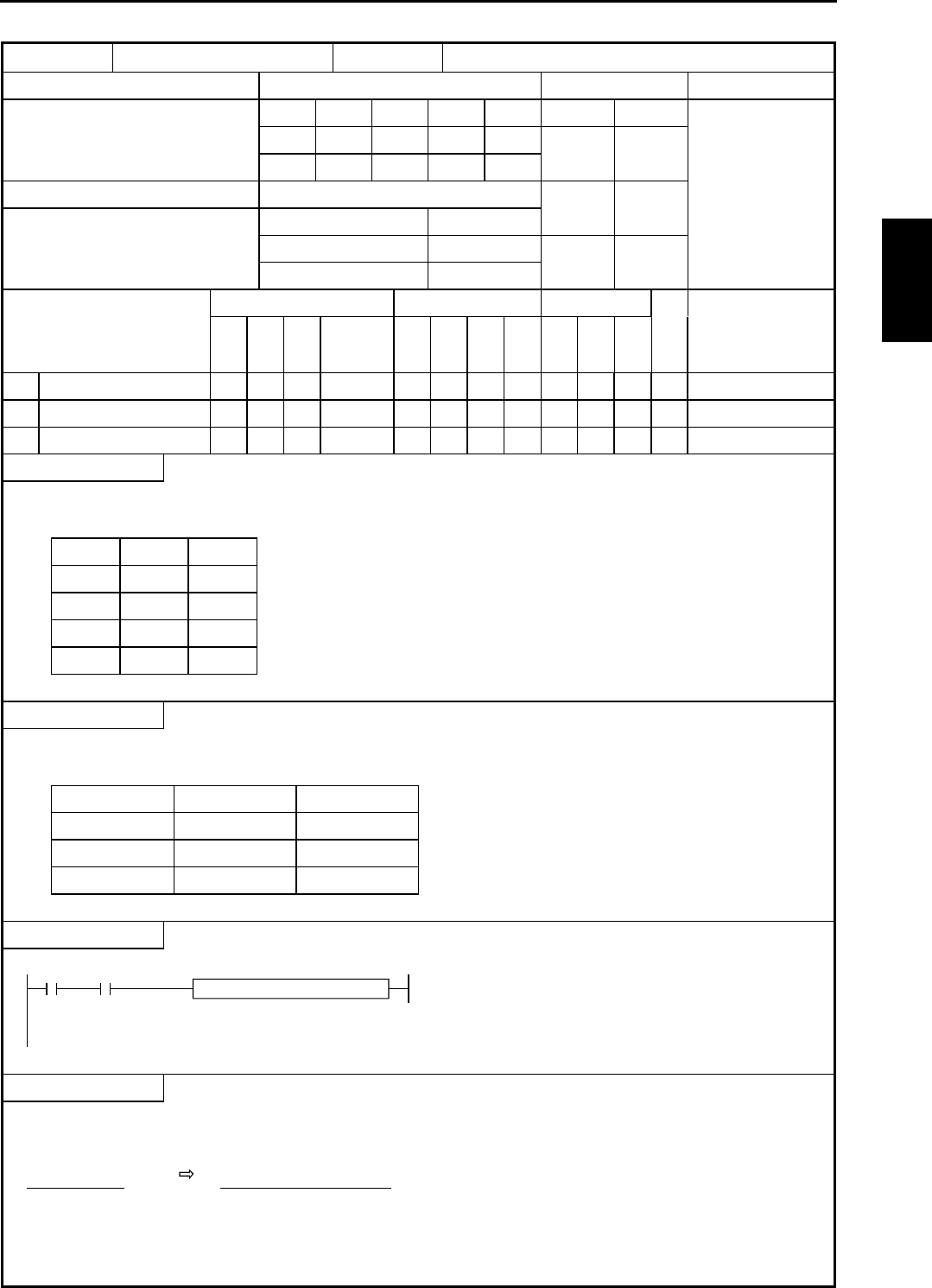
Chapter 5 Instruction Specifications
5-59
Item number Arithmetic instructions-14 Name Exclusive OR
Ladder format Condition code Processing time (µs) Remark
R7F4 R7F3 R7F2 R7F1 R7F0 Average Maximum
d = s1 XOR s2 DER ERR SD V C 42 Upper case: B
zzzzz Middle case: W
Instruction format Number of steps 33 Lower case: DW
Condition Steps
d = s1 XOR s2 Bit, word 4 66
Double word 6
Bit Word Double word
Usable I/O XY
R,
M
TD, SS,
CU, CT WX WY
WR,
WM TC DX DY
DR,
DM
Constant
Other
d Substitution destination {{ {{{ {{
s1 Comparand {{{ {{{{{{{{
s2 Relational number {{{ {{{{{{{{
Function
•Obtains exclusive OR (XOR) of s1 and s2, and substitutes the result into d.
s1 s2 d
000
011
101
110
Notes
•The combinations of d, s1 and s2 are as follows:
ds1s2
Bit Bit Bit
Word Word Word
Double word Double word Double word
Program example
WR0102= WR0100 XOR WR0101
X00112 DIF112 LD X00112
AND DIF112
[
WR0102=WR0100 XOR WR0101
]
Program description
•At the leading edge of X00112, the XOR of WR0100 and WR0101 is set in WR0102.
WR0100 = H1234
WR0101 = H5678
WR0102 = H444C
WR0100 = 0001001000110100
WR0101 = 0101011001111000
WR0102 = 0100010001001100
When
d = s1 XOR s2

Chapter 5 Instruction Specifications
5-60
Item number Arithmetic instructions-15 Name = Relational expression
Ladder format Condition code Processing time (µs) Remark
R7F4 R7F3 R7F2 R7F1 R7F0 Average Maximum
d = s1 == s2 DER ERR SD V C
zzzzz 60
Instruction format Number of steps
Condition Steps
d = s1 == s2 s is a word 4 48
s is a double word 6
Bit Word Double word
Usable I/O XY
R,
M
TD, SS,
CU, CT WX WY
WR,
WM TC DX DY
DR,
DM
Constant
Other
d Substitution destination {{
s1 Comparand {{{{{{{{
s2 Relational number {{{{{{{{
Function
•Substitutes “1” when s1 is equal to s2 and otherwise “0” into d, assuming s1 and s2 as binary data.
Notes
•The combinations of d, s1 and s2 are as follows:
ds1s2
Bit Word Word
Bit Double word Double word
Program example
M0000 = WX0000 = = WX0001
[
M0000 = WX0000 = = WX0001
]
Program description
•When WX0000 = WX0001, M0000 is set to “1.” Otherwise, M0000 is reset to “0.”
d = s1 == s2

Chapter 5 Instruction Specifications
5-61
Item number Arithmetic instructions-16 Name Signed = Relational expression
Ladder format Condition code Processing time (µs) Remark
R7F4 R7F3 R7F2 R7F1 R7F0 Average Maximum
d = s1 S== s2 DER ERR SD V C
zzzzz
Command format Number of steps 108
Condition Steps
d = s1 S== s2 s is a double word 6
Bit Word Double word
Usable I/O XY
R,
L,
M
TD, SS,
CU, CT WX WY
WR,
WM TC DX DY
DR,
DM
Constant
Other
d Substitution destination {{
s1 Comparand {{{{
s2 Relational number {{{{
Function
z Substitutes 1 when s1 is equal to s2 and otherwise 0 into d, assuming s1 and s2 as signed binary data.
z s1 and s2 are both signed binary data. When the most significant bit is 0, the value is positive; when the most significant
bit is 1, the value is negative.
s1, s2 – 2147483648 to +2147483647 (decimal)
H80000000 to H7FFFFFFF (hexadecimal)
b
31 b16 b15 b0
Sign bit: 0 - Positive; 1 - Negative
Program example
M0000 = DR0000 S== DR0002
[
M0000 = DR0000 S== DR0002
]
Program description
z When the values of DR0000 and DR0002 are equal, 1 is set in M0000. Otherwise, M0000 is reset to 0.
d = s1 S== s2

Chapter 5 Instruction Specifications
5-62
Item number Arithmetic instructions-17 Name <> Relational expression
Ladder format Condition code Processing time (µs) Remark
R7F4 R7F3 R7F2 R7F1 R7F0 Average Maximum
d = s1 <> s2 DER ERR SD V C
zzzzz 60
Instruction format Number of steps
Condition Steps
d = s1 <> s2 s is a word 4 46
s is a double Word 6
Bit Word Double word
Usable I/O XY
R,
M
TD, SS,
CU, CT WX WY
WR,
WM TC DX DY
DR,
DM
Constant
Other
d Substitution destination {{
s1 Comparand {{{{{{{{
s2 Relational number {{{{{{{{
Function
•Substitutes 1 when s1 is not equal to s2 and otherwise 0 into d, assuming s1 and s2 as binary data.
Notes
•The combinations of d, s1 and s2 are as follows:
ds1s2
Bit Word Word
Bit Double word Double word
Program example
Y00000= WR0000 < > WR0001
[
Y00000= WR0000 < > WR0001
]
Program description
•When WR0000 ≠ WR0001, “1” is set in Y00000. Otherwise, Y00000 is reset to “0.”
d = s1 <> s2
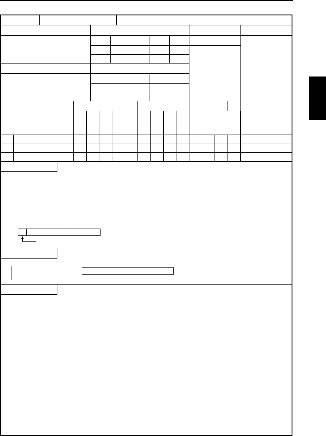
Chapter 5 Instruction Specifications
5-63
Item number Arithmetic instructions-18 Name Signed <> Relational expression
Ladder format Condition code Processing time (µs) Remark
R7F4 R7F3 R7F2 R7F1 R7F0 Average Maximum
d = s1 S<> s2 DER ERR SD V C
zzzzz
Command format Number of steps 48
Condition Steps
d = s1 S<> s2 s is a double word 6
Bit Word Double word
Usable I/O XY
R,
L,
M
TD, SS,
CU, CT WX WY
WR,
WM TC DX DY
DR,
DM
Constant
Other
d Substitution destination {{
s1 Comparand {{{{
s2 Relational number {{{{
Function
z Substitutes 1 when s1 is not equal to s2 and otherwise 0 into d, assuming s1 and s2 as signed binary data.
z s1 and s2 are both signed binary data. When the most significant bit is 0, the value is positive; when the most significant
bit is 1, the value is negative.
s1, s2 – 2147483648 to +2147483647 (decimal)
H80000000 to H7FFFFFFF (hexadecimal)
b31 b16 b15 b0
Sign bit: 0 - Positive; 1 - Negative
Program example
Y00100 = DR0000 S<> DR0002
[
Y00100 = DR0000 S<> DR0002
]
Program description
z When the values of DR0000 and DR0002 are not equal, Y00100 is turned on. Otherwise, Y00100 is turned off.
d = s1 S<> s2
Chapter 5 Instruction Specifications
5-64
Item number Arithmetic instructions-19 Name < Relational expression
Ladder format Condition code Processing time (µs) Remark
R7F4 R7F3 R7F2 R7F1 R7F0 Average Maximum
d = s1 < s2 DER ERR SD V C Upper case: W
zzzzz 40 Lower case: DW
Instruction format Number of steps
Condition Steps
d = s1 < s2 s is a word 4 70
s is a double word 6
Bit Word Double word
Usable I/O XY
R,
M
TD, SS,
CU, CT WX WY
WR,
WM TC DX DY
DR,
DM
Constant
Other
d Substitution destination {{
s1 Comparand {{{{{{{{
s2 Relational number {{{{{{{{
Function
•Substitutes “1” when s1 is less than s2 and otherwise “0” into d, assuming s1 and s2 as binary data.
Notes
•The combinations of d, s1 and s2 are as follows:
ds1s2
Bit Word Word
Bit Double word Double word
Program example
R0 = TC100 < TC101
[
R0 = TC100 < TC101
]
Program description
•When TC100 < TC101, R0 is set to “1.” Otherwise, R0 is reset to “0.”
(TC n is the progress value of the no. n timer or counter.)
d = s1 < s2

Chapter 5 Instruction Specifications
5-65
Item number Arithmetic instructions-20 Name Signed < Relational expression
Ladder format Condition code Processing time (µs) Remark
R7F4 R7F3 R7F2 R7F1 R7F0 Average Maximum
d = s1 S< s2 DER ERR SD V C
zzzzz
Command format Number of steps 50
Condition Steps
d = s1 S< s2 s is a double word 6
Bit Word Double word
Usable I/O XY
R,
L,
M
TD, SS,
CU, CT WX WY
WR,
WM TC DX DY
DR,
DM
Constant
Other
d Substitution destination {{
s1 Comparand {{{{
s2 Relational number {{{{
Function
z Substitutes 1 when s1 is less than s2 and otherwise 0 into d, assuming s1 and s2 as signed binary data.
z s1 and s2 are both signed binary data. When the most significant bit is 0, the value is positive; when the most significant
bit is 1, the value is negative.
s1, s2 – 2147483648 to +2147483647 (decimal)
H80000000 to H7FFFFFFF (hexadecimal)
b31 b16 b15 b0
Sign bit: 0 - Positive; 1 - Negative
Program example
R100 = DM000 S< DM002
[
R100 = DM000 S< DM002
]
Program description
z When the value in DM000 is less than the value in DM002, 1 is set in R100. Otherwise, R100 is reset to 0.
d = s1 S< s2

Chapter 5 Instruction Specifications
5-66
Item number Arithmetic instructions-21 Name ≤ Relational expression
Ladder format Condition code Processing time (µs) Remark
R7F4 R7F3 R7F2 R7F1 R7F0 Average Maximum
d = s1 <= s2 DER ERR SD V C Upper case: W
zzzzz 40 Lower case: DW
Instruction format Number of steps
Condition Steps
d = s1 <= s2 s is a word 4 71
s is a double word 6
Bit Word Double word
Usable I/O XY
R,
M
TD, SS,
CU, CT WX WY
WR,
WM TC DX DY
DR,
DM
Constant
Other
d Substitution destination {{
s1 Comparand {{{{{{{{
s2 Relational number {{{{{{{{
Function
•Substitutes “1” when s1 is less than or equal to s2 and otherwise “0” into d, assuming s1 and s2 as binary data.
Notes
•The combinations of d, s1 and s2 are as follows:
ds1s2
Bit Word Word
Bit Double word Double word
Program example
Y00001 = WR10 <= WR100
[
Y00001 = WR10 <= WR100
]
Program description
•When WR10 ≤ WR100, Y00001 is set to “1.” Otherwise, Y00001 is reset to “0.”
d = s1 <= s2

Chapter 5 Instruction Specifications
5-67
Item number Arithmetic instructions-22 Name Signed ≤ Relational expression
Ladder format Condition code Processing time (µs) Remark
R7F4 R7F3 R7F2 R7F1 R7F0 Average Maximum
d = s1 S<= s2 DER ERR SD V C
zzzzz
Command format Number of steps 50
Condition Steps
d = s1 S<= s2 s is a double word 6
Bit Word Double word
Usable I/O XY
R,
L,
M
TD, SS,
CU, CT WX WY
WR,
WM TC DX DY
DR,
DM
Constant
Other
d Substitution destination {{
s1 Comparand {{{{
s2 Relational number {{{{
Function
z Substitutes 1 when s1 is less than or equal to s2 and otherwise 0 into d, assuming s1 and s2 as signed binary data.
z s1 and s2 are both signed binary data. When the most significant bit is 0, the value is positive; when the most significant
bit is 1, the value is negative.
s1, s2 – 2147483648 to +2147483647 (decimal)
H80000000 to H7FFFFFFF (hexadecimal)
b31 b16 b15 b0
Sign bit: 0 - Positive; 1 - Negative
Program example
Y00100 = DR10 S<= DR100
[
Y00100 = DR10 S<= DR100
]
Program description
z When the value in DR10 is less than or equal the value in DR100, Y00100 is turned on. Otherwise, Y00100 is turned off.
d = s1 S<= s2
Chapter 5 Instruction Specifications
5-68
Item number Application instructions-1 Name Bit set
Ladder format Condition code Processing time (µs) Remark
R7F4 R7F3 R7F2 R7F1 R7F0 Average Maximum
BSET (d, n) DER ERR SD V C Upper case: W
zzzzz 26 Lower case: DW
Instruction format Number of steps
Condition Steps
BSET (d, n) 3 35
Bit Word Double word
Usable I/O XY
R,
M
TD, SS,
CU, CT WX WY
WR,
WM TC DX DY
DR,
DM
Constant
Other
d I/O to be set the bit {{{ {{
n Bit location to be set {{{{ {
The constant is set in
decimal.
Function
•Sets the nth bit in the I/O (word or double word) specified by d to “1.”
•Other bit contents are unaltered.
. . . . . . . . . . . . . . . . . . 5
d
43210n
1
n-1n+1
“1” is set.
. . . . . . . . . . . . . . . . . . . . . . . .
If d is a word: Designates the bit location depending on the contents (0 to 15) of the lower 4 bits (b3 to b0) of n (WX,
WY, WR, WM, TC). (Upper bits are ignored and considered as “0.”)
The n (constant) can be set to 0 to 15 (decimal).
If d is a double word: Designates the bit location depending on the contents (0 to 31) of the lower 5 bits (b4 to b0) of n (WX,
WY, WR, WM, TC). (Upper bits are ignored and considered as “0.”)
The n (constant) can be set to 0 to 31 (decimal).
BEST (d, n)

Chapter 5 Instruction Specifications
5-69
Item number Application instructions-2 Name Bit reset
Ladder format Condition code Processing time (µs) Remark
R7F4 R7F3 R7F2 R7F1 R7F0 Average Maximum
BRES (d, n) DER ERR SD V C Upper case: W
zzzzz 29 Lower case: DW
Instruction format Number of steps
Condition Steps
BRES (d, n) 3 38
Bit Word Double word
Usable I/O XY
R,
M
TD, SS,
CU, CT WX WY
WR,
WM TC DX DY
DR,
DM
Constant
Other
d I/O to be set the bit {{{ {{
n Bit location to be reset {{{{ {
The constant is set in
decimal.
Function
•Sets the nth bit in the I/O (word or double word) specified by d to “0.”
•Other bit contents are unaltered.
5
d
43210n
0
n-1n+1
Reset to “0”.
. . . . . . . . . . . . . . . . . . . . . . . . . . . . . . . . . . . . . . . . . .
If d is a word: Designates the bit location depending on the contents (0 to 15) of the lower 4 bits (b3 to b0) of n (WX,
WY, WR, WM, TC). (Upper bits are ignored and considered as “0.”)
The n (constant) can be set to 0 to 15 (decimal).
If d is a double word: Designates the bit location depending on the contents (0 to 31) of the lower 5 bits (b4 to b0) of n (WX,
WY, WR, WM, TC). (Upper bits are ignored and considered as “0.”)
The n (constant) can be set to 0 to 31 (decimal).
BRES (d, n)

Chapter 5 Instruction Specifications
5-70
Item number Application instructions-3 Name Bit test
Ladder format Condition code Processing time (µs) Remark
R7F4 R7F3 R7F2 R7F1 R7F0 Average Maximum
BTS (d, n) DER ERR SD V C Upper case: W
zzzz ↕31 Lower case: DW
Instruction format Number of steps
Condition Steps
BTS (d, n) 3 38
Bit Word Double word
Usable I/O XY
R,
M
TD, SS,
CU, CT WX WY
WR,
WM TC DX DY
DR,
DM
Constant
Other
d I/O to be tested {{{ {{
n Bit location to be tested {{{{ {
The constant is set in
decimal.
Function
•Checks the contents of the nth bit of the I/O (word or double word) specified by d, and if the result is “1,” '1' is set to C
(R7F0). If the result is “0,” C (R7F0) is reset to “0.”
•The contents of d remains unaltered.
5
d
C (R7F0)
43210nn-1n+1
. . . . . . . . . . . . . . . . . . . . . . . . . . . . . . . . . . . . . . . . . .
If d is a word: Designates the bit location depending on the contents (0 to 15) of the lower 4 bits (b3 to b0) of n (WX,
WY, WR, WM, TC). (Upper bits are ignored and considered as “0.”)
The n (constant) can be set to 0 to 15 (decimal).
If d is a double word: Designates the bit location depending on the contents (0 to 31) of the lower 5 bits (b4 to b0) of n (WX,
WY, WR, WM, TC). (Upper bits are ignored and considered as “0.”)
The n (constant) can be set to 0 to 31 (decimal).
Program example
BSET
(
DR0100, WR0001
)
BRES
(
DR0102, WR0001
)
BTS
(
DR0104, WR0001
)
R000 = R7F0
X00000 DIF200 LD X00000
AND DIF200
[
BSET
(
DR0100, WR0001
)
BRES
(
DR0102, WR0001
)
BTS
(
DR0104, WR0001
)
R000 = R7F0
]
BTS (d, n)

Chapter 5 Instruction Specifications
5-71
Program description
When WR0001 = H1234 at the leading edge of X00000 (WR0001 = 0001001000110100)
20 (decimal)
If DR0100 = H00000000, DR0102 = HFFFFFFFF and DR0104 = H5555AAAA are set, the 20th bit of DR0100 is set to “1” by
the BSET at the leading edge of X00000.
D
R0100=00000000000000000000000000000000
b31 b20 b0
This bit is set to “1.”
Also, the 20th bit of DR0102 is reset to “0” by BRES.
D
R0102=11111111111111111111111111111111
b31 b20 b0
This bit is set to “0.”
Also, the 20th bit of DR0104 is checked by BTS.
DR0104=01010101010101011010101010101010
b31 b20 b0
This bit is checked.
Since the 20th bit is “1,” C (R7F0) = “1” is set.
BTS (d, n)
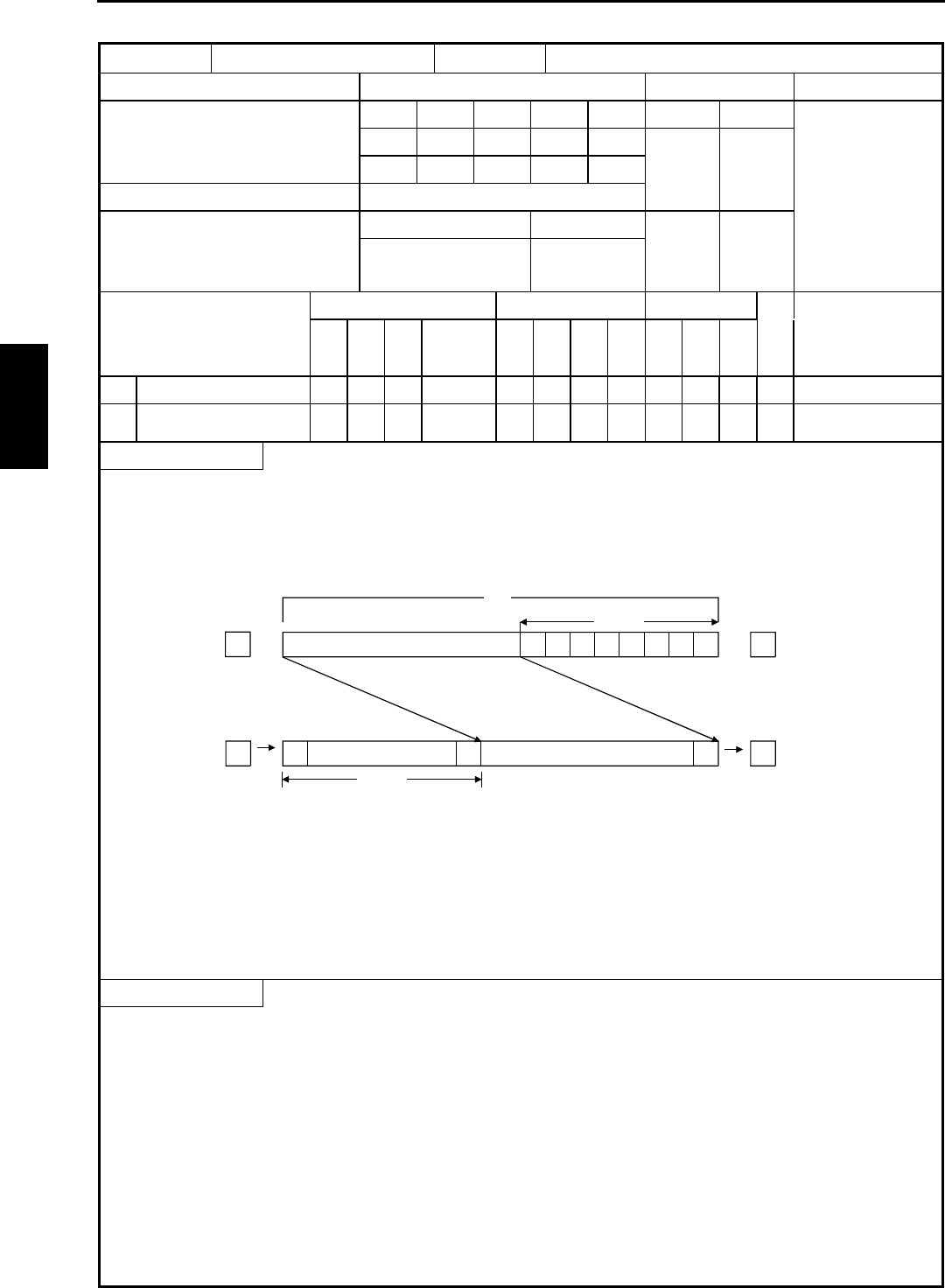
Chapter 5 Instruction Specifications
5-72
Item number Application instructions-4 Name Shift right
Ladder format Condition code Processing time (µs) Remark
R7F4 R7F3 R7F2 R7F1 R7F0 Average Maximum
SHR (d, n) DER ERR SD V C Upper case: W
zzzz ↕38 Lower case: DW
Instruction format Number of steps
Condition Steps
SHR (d, n) 3 46
Bit Word Double word
Usable I/O XY
R,
M
TD, SS,
CU, CT WX WY
WR,
WM TC DX DY
DR,
DM
Constant
Other
d I/O to be shifted {{{ {{
nNumber of bits to be
shifted {{{{ {
The constant is set in
decimal.
Function
•Shifts the contents of d to the right (toward the lower digits) by n bits.
•Sets n bits of SD (R7F2) contents starting with the most significant bit.
•Sets the content of the nth bit from the least significant bit in C (R7F0).
SD
SD SD SD SD
SD B
C (R7F0)
SD (R7F2)
d
B
Least significant bit (LSB)Most significant bit (MSB)
n bits
n bits
Before execution
After execution
If d is a word: Designates the shift amount, depending on the contents (0 to 15) of the lower 4 bits (b3 to b0) of n
(WX, WY, WR, WM, TC). (Upper bits are ignored and considered as “0.”)
The n (constant) can be set to 0 to 15 (decimal).
If d is a double word: Designates the shift amount, depending on the contents (0 to 31) of the lower 5 bits (b4 to b0) of n
(WX, WY, WR, WM, TC). (Upper bits are ignored and considered as “0.”)
The n (constant) can be set to 0 to 31 (decimal).
Notes
•If n is equal to “0,” the shifting is not performed. The previous state is retained in C.
SHR (d, n)
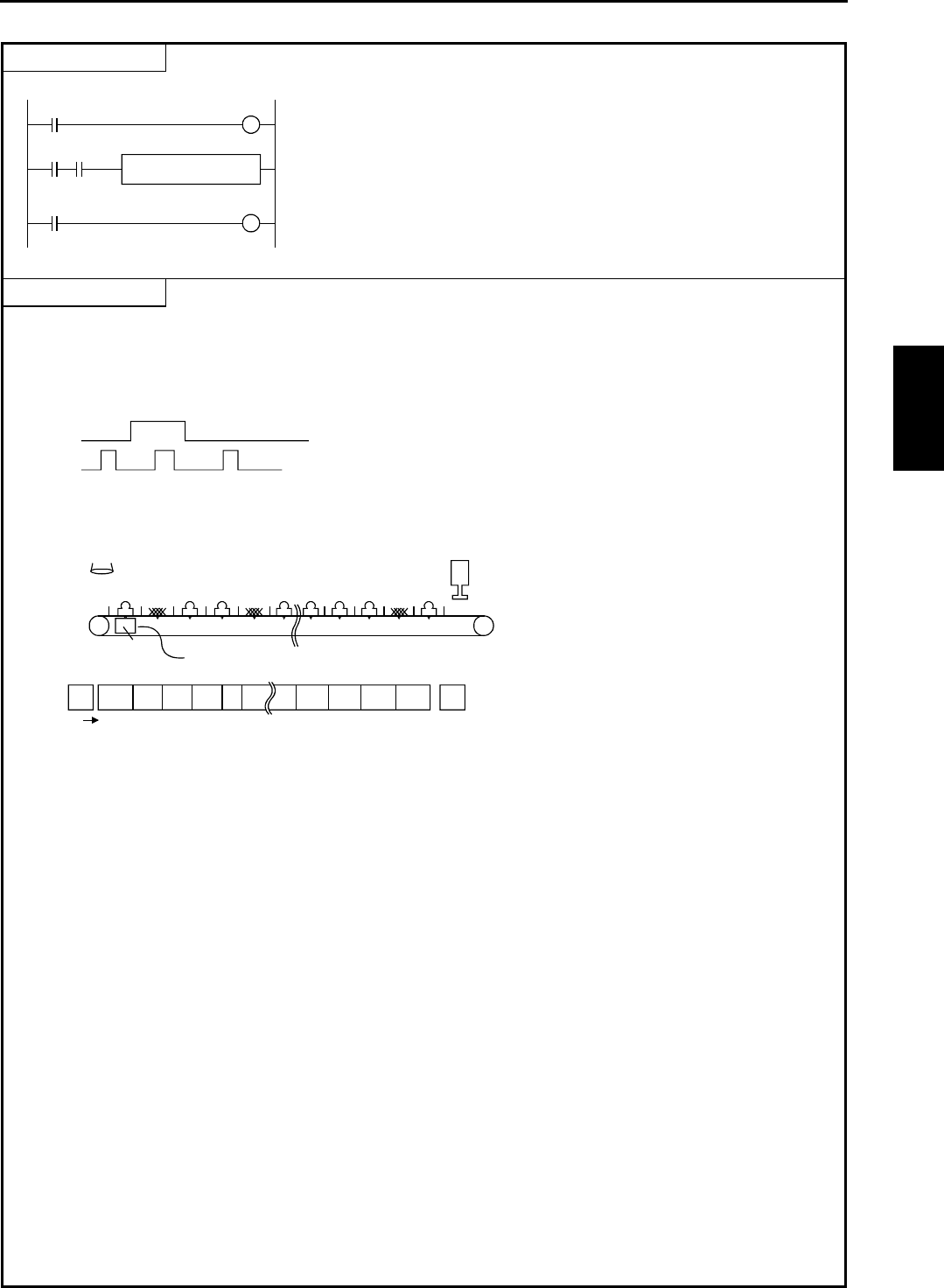
Chapter 5 Instruction Specifications
5-73
Program example
X00000
X00001 DIF1
R7F2
R7F0 Y00100
SHR (DR0000,1)
X00000 . . . . .
X00001 . . . . .
. . . . .
LD X00000
OUT R7F2
LD X00001
AND DIF1
[
SHR (DR0000,1)
]
LD R7F0
OUT Y00100
Defective unit input
To SD
Conveyor movement
Defective unit output
Carry
Y00001
Program description
•There exists a conveyor that has 16 stands and is moving to the right.
•Each time the conveyor moves one stand to the right, a pulse input enters X1.
•There is a sensor on the left end of the conveyor, and when a defective unit is placed on the conveyor, X00000 turns on.
X00000 (sensor input) and X00001 (conveyor movement) signals are as follows:
X00000
X00001
•As the conveyor moves to the right, the data is also shifted one bit at a time, and when data exits to the carry (on the right
end of the conveyor), the (Y00100) solenoid valve turns on and rejects the defective unit.
b16
(Y00100)
b0
X00001
01001000 0 1 0
b16 b0
SD (R7F2)
X00000
C (R7F0)
Y00000
Sensor (X00000)
Solenoid valve
Conveyor movement
Shifts one bit at a time
SHR (d, n)

Chapter 5 Instruction Specifications
5-74
Item number Application instructions-5 Name Shift left
Ladder format Condition code Processing time (µs) Remark
R7F4 R7F3 R7F2 R7F1 R7F0 Average Maximum
SHL (d, n) DER ERR SD V C Upper case: W
zzzz ↕38 Lower case: DW
Instruction format Number of steps
Condition Steps
SHL (d, n) 3 46
Bit Word Double word
Usable I/O XY
R,
M
TD, SS,
CU, CT WX WY
WR,
WM TC DX DY
DR,
DM
Constant
Other
d I/O to be shifted {{{ {{
nNumber of bits to be
shifted {{{{ {
The constant is set in
decimal.
Function
•Shifts the contents of d to the left (toward the upper digits) by n bits.
•Sets n bits of SD (R7F2) contents starting with the least significant bit.
•Sets the content of the nth bit from the most significant bit in C (R7F0).
SD
BSD SD SD
SD SD
SD (R7F2)
C (R7F0)
B
d
n bits
Most significant bit (MSB) Least significant bit (LSB)
B
efore execution
A
fter execution
n bits
If d is a word: Designates the shift amount, depending on the contents (0 to 15) of the lower 4 bits (b3 to b0) of n
(WX, WY, WR, WM, TC). (Upper bits are ignored and considered as “0.”)
The n (constant) can be set to 0 to 15 (decimal).
If d is a double word: Designates the shift amount, depending on the contents (0 to 31) of the lower 5 bits (b4 to b0) of n
(WX, WY, WR, WM, TC). (Upper bits are ignored and considered as “0.”)
The n (constant) can be set to 0 to 31 (decimal).
Notes
•If n is equal to “0,” the shifting is not performed. The previous state is retained in C.
Program example
X00000 LD X00000
OUT R7F2
LD X00001
AND DIF1
[
SHL (DR0000,1)
]
LD R7F0
OUT Y00100
X00001 DIF1
SHL (DR0000 ,1 )
R7F2
R7F0 Y00100
Program description
•The R7F2 value is determined by the on/off of X00000.
•The content of DR0000 is shifted to the left by one bit when X00001 rises.
At this time, the value of R7F2 is set in b0 and the value of b31 (b15 of WR1) in R7F0.
•The Y00100 turns on/off depending on the b31 value of DR0000 (b15 of WR1) prior to the shift.
SHL (d, n)

Chapter 5 Instruction Specifications
5-75
Item number Application instructions-6 Name Rotate right
Ladder format Condition code Processing time (µs) Remark
R7F4 R7F3 R7F2 R7F1 R7F0 Average Maximum
ROR (d, n) DER ERR SD V C Upper case: W
zzzz ↕47 Lower case: DW
Instruction format Number of steps
Condition Steps
ROR (d, n) 3 75
Bit Word Double word
Usable I/O XY
R,
M
TD, SS,
CU, CT WX WY
WR,
WM TC DX DY
DR,
DM
Constant
Other
d I/O to be rotated {{{ {{
nNumber of bits to be
rotated {{{{ {
The constant is set in
decimal.
Function
•Rotates the contents of d to the right (toward the lower digits) by n bits.
•The content of the least significant bit is input to C (R7F0) while the content of C (R7F0) is input to the most significant bit.
This is repeated n times.
•The content of C (R7F0) is set in the nth bit from the most significant bit.
•The content of the nth bit from the least significant bit is set in C (R7F0).
Bn
C (R7F0)
d
Bn-1
Bn B3 B2 B1
B3 B2 B1 C
n bits
Most significant bit (MSB) Least significant bit (LSB)
B
efore execution
A
fter execution
n bits
If d is a word: Designates the shift amount, depending on the contents (0 to 15) of the lower 4 bits (b3 to b0) of n
(WX, WY, WR, WM, TC). (Upper bits are ignored and considered as “0.”)
The n (constant) can be set to 0 to 15 (decimal).
If d is a double word: Designates the shift amount, depending on the contents (0 to 31) of the lower 5 bits (b4 to b0) of n
(WX, WY, WR, WM, TC). (Upper bits are ignored and considered as “0.”)
The n (constant) can be set to 0 to 31 (decimal).
Notes
•If n is equal to “0,” the rotation is not performed. The previous state is retained in C.
Program example
R000 DIF0 R0R (WR0000 ,1 )
LD R000
AND DIF0
[
R0R (WR0000,1)
]
Program description
•When R000 rises, WR0000 is shifted to the right by one bit.
At this time, the value of the least significant bit, b0, is set in R7F0, and the value of R7F0 immediately prior to the shift is
set in the most significant bit, b15.
ROR (d, n)

Chapter 5 Instruction Specifications
5-76
Item number Application instructions-7 Name Rotate left
Ladder format Condition code Processing time (µs) Remark
R7F4 R7F3 R7F2 R7F1 R7F0 Average Maximum
ROL (d, n) DER ERR SD V C Upper case: W
zzzz ↕46 Lower case: DW
Instruction format Number of steps
Condition Steps
ROL (d, n) 3 54
Bit Word Double word
Usable I/O XY
R,
M
TD, SS,
CU, CT WX WY
WR,
WM TC DX DY
DR,
DM
Constant
Other
d I/O to be rotated {{{ {{
nNumber of bits to be
rotated {{{{ {
The constant is set in
decimal.
Function
•Rotates the contents of d to the left (toward the upper digits) by n bits.
•The content of C (R7F0) is set in the nth bit from the least significant bit.
•The content of the nth bit from the least significant bit is set in C (R7F0).
Bn
C (R7F0)
d
BnB1 B2 B3
C B1 B2 B3 Bn-1
Least significant bit (LSB)
Before execution
After execution
n bits
Most significant bit (MSB)
n bits
If d is a word: Designates the shift amount, depending on the contents (0 to 15) of the lower 4 bits (b3 to b0) of n
(WX, WY, WR, WM, TC). (Upper bits are ignored and considered as “0.”)
The n (constant) can be set to 0 to 15 (decimal).
If d is a double word: Designates the shift amount, depending on the contents (0 to 31) of the lower 5 bits (b4 to b0) of n
(WX, WY, WR, WM, TC). (Upper bits are ignored and considered as “0.”)
The n (constant) can be set to 0 to 31 (decimal).
Notes
•If n is equal to “0,” the rotation is not performed. The previous state is retained in C.
ROL (d, n)

Chapter 5 Instruction Specifications
5-77
Program example
R7F0= 0
ROL(DR0000,1)
ROL(DR0002,1)
X00001 DIF1 LD X00001
AND DIF1
[
R7F0 = 0
ROL (DR0000,1)
ROL (DR0002,1)
]
Program description
•When X00001 rises, the 64-bit data is shifted one bit at a time.
The space after the shift is filled with “0.”
Overall movement
C
0
b31 DR0002 b0 C b31 DR0000 b0 C
0
(R7F0)
DR0000 b31
ROL (d, n)

Chapter 5 Instruction Specifications
5-78
Item number Application instructions-8 Name Logical shift right
Ladder format Condition code Processing time (µs) Remark
R7F4 R7F3 R7F2 R7F1 R7F0 Average Maximum
LSR (d, n) DER ERR SD V C Upper case: W
zzzz ↕36 Lower case: DW
Instruction format Number of steps
Condition Steps
LSR (d, n) 3 45
Bit Word Double word
Usable I/O XY
R,
M
TD, SS,
CU, CT WX WY
WR,
WM TC DX DY
DR,
DM
Constant
Other
d I/O to be shifted {{{ {{
nNumber of bits to be
shifted {{{{ {
The constant is set in
decimal.
Function
•Shifts the contents of d to the right (toward the lower digits) by n bits.
•“0” is set from the most significant bit to the nth bit.
•The content of the nth bit from the least significant bit is set in C (R7F0).
000 00 B
C (R7F0)
(R7F0)
B
d
n bits
Most significant bit (MSB) Least significant bit (LSB)
Before execution
After execution
n bits
If d is a word: Designates the shift amount, depending on the contents (0 to 15) of the lower 4 bits (b3 to b0) of n
(WX, WY, WR, WM, TC). (Upper bits are ignored and considered as “0.”)
The n (constant) can be set to 0 to 15 (decimal).
If d is a double word: Designates the shift amount, depending on the contents (0 to 31) of the lower 5 bits (b4 to b0) of n
(WX, WY, WR, WM, TC). (Upper bits are ignored and considered as “0.”)
The n (constant) can be set to 0 to 31 (decimal).
Notes
•If n is equal to “0,” the shifting is not performed. The previous state is retained in C.
Program example
X00001 DIF1 LSR (WR0000 ,1 )
LD X00001
AND DIF1
[
LSR (WR0000 ,1)
]
Program description
•When X00001 rises, the content of WR0000 is shifted to the right by one bit.
At this time, “0” is set in b15 and the value of b0 immediately prior to the shift is set in R7F0.
LSR (d, n)

Chapter 5 Instruction Specifications
5-79
Item number Application instructions-9 Name Logical shift left
Ladder format Condition code Processing time (µs) Remark
R7F4 R7F3 R7F2 R7F1 R7F0 Average Maximum
LSL (d, n) DER ERR SD V C Upper case: W
zzzz ↕36 Lower case: DW
Instruction format Number of steps
Condition Steps
LSL (d, n) 3 45
Bit Word Double word
Usable I/O XY
R,
M
TD, SS,
CU, CT WX WY
WR,
WM TC DX DY
DR,
DM
Constant
Other
d I/O to be shifted {{{ {{
nNumber of bits to be
shifted {{{{ {
The constant is set in
decimal.
Function
•Shifts the contents of d to the left (toward the upper digits) by n bits.
• “0” is set from the least significant bit to the nth bit.
•The content of the nth bit from the most significant bit is set in C (R7F0).
0
00 00
B
B
C (R7F0)
d
n bits
Most significant bit (MSB) Least significant bit (LSB)
Before execution
After execution
n bits
If d is a word: Designates the shift amount, depending on the contents (0 to 15) of the lower 4 bits (b3 to b0) of n
(WX, WY, WR, WM, TC). (Upper bits are ignored and considered as “0.”)
The n (constant) can be set to 0 to 15 (decimal).
If d is a double word: Designates the shift amount, depending on the contents (0 to 31) of the lower 5 bits (b4 to b0) of n
(WX, WY, WR, WM, TC). (Upper bits are ignored and considered as “0.”)
The n (constant) can be set to 0 to 31 (decimal).
Notes
•If n is equal to “0,” the shifting is not performed. The previous state is retained in C.
Program example
X00001 DIF1 LSL (WR0000 ,1 )
LD X00001
AND DIF1
[
LSL (WR0000 ,1)
]
Program description
•When X00001 rises, the content of WR0000 is shifted to the left by one bit.
At this time, “0” is set in b0 and the value of b15 immediately prior to the shift is set in R7F0.
LSL (d, n)
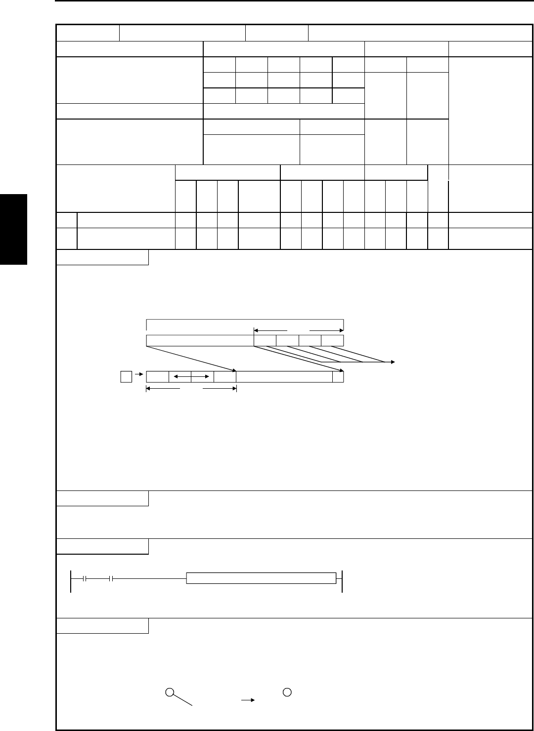
Chapter 5 Instruction Specifications
5-80
Item number Application instructions-10 Name BCD shift right
Ladder format Condition code Processing time (µs) Remark
R7F4 R7F3 R7F2 R7F1 R7F0 Average Maximum
BSR (d, n) DER ERR SD V C Upper case: W
zzzzz 32 Lower case: DW
Instruction format Number of steps
Condition Steps
BSR (d, n) 3 40
Bit Word Double word
Usable I/O XY
R,
M
TD, SS,
CU, CT WX WY
WR,
WM TC DX DY
DR,
DM
Constant
Other
d I/O to be shifted {{{ {{
nNumber of digits to be
shifted {{{{ {
The constant is set in
decimal.
Function
•Shifts the contents of d to the right (toward the lower digits) by n digits (1 digit is equivalent to 4 bits).
•“0” is set from the most significant bit to the nth digit.
•The digits from least significant bit to the nth digit are discarded.
00000 0000
n digits
n digits
Most significant bit (MSB) Least significant bit (LSB)
Before execution
After execution Discarded
If d is a word: Designates the shift amount, depending on the contents (0 to 3) of the lower 2 bits (b1, b0) of n (WX,
WY, WR, WM, TC). (Upper bits are ignored and considered as “0.”)
The n (constant) can be set to 0 to 3 (decimal).
If d is a double word: Designates the shift amount, depending on the contents (0 to 7) of the lower 3 bits (b2 to b0) of n
(WX, WY, WR, WM, TC). (Upper bits are ignored and considered as “0.”)
The n (constant) can be set to 0 to 7 (decimal).
Notes
•If n is equal to “0,” the shifting is not performed.
Program example
X00001 DIF1 BSR (WR0000 ,1 )
LD X00001
AND DIF1
[
BSR (WR0000 ,1)
]
Program description
•When X00001 rises, the content of WR0000 is regarded as BCD code and shifted to the right by four bits.
At this time, the values in the lower 4 bits (b3 to b0) are deleted and “0000” is set in the upper four bits (b12 to b15).
H
1 2 3 4
0000 0001 0010 0011
0001 0010 0011 0100
Before the shift After the shift
Deleted Set to “0”
H 0 1 2 3
BSR (d, n)
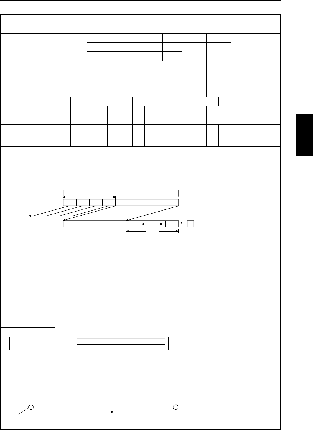
Chapter 5 Instruction Specifications
5-81
Item number Application instructions-11 Name BCD shift left
Ladder format Condition code Processing time (µs) Remark
R7F4 R7F3 R7F2 R7F1 R7F0 Average Maximum
BSL (d, n) DER ERR SD V C Upper case: W
zzzzz 32 Lower case: DW
Instruction format Number of steps
Condition Steps
BSL (d, n) 3 39
Bit Word Double word
Usable I/O XY
R,
M
TD, SS,
CU, CT WX WY
WR,
WM TC DX DY
DR,
DM
Constant
Other
d I/O to be shifted {{{ {{
nNumber of digits to be
shifted {{{{ {
The constant is set in
decimal.
Function
•Shifts the contents of d to the left (toward the upper digits) by n digits (one digit is equivalent to 4 bits).
•“0” is set from the least significant bit to the nth digit.
•The digits from the most significant bit to the nth digit are discarded.
0
0000
d
0000
n digits
Most significant bit (MSB) Least significant bit (LSB)
Discarded
Before execution
After execution
n digits
If d is a word: Designates the shift amount, depending on the contents (0 to 3) of the lower 2 bits (b1, b0) of n (WX,
WY, WR, WM, TC). (Upper bits are ignored and considered as “0.”)
The n (constant) can be set to 0 to 3 (decimal).
If d is a double word: Designates the shift amount, depending on the contents (0 to 7) of the lower 3 bits (b2 to b0) of n
(WX, WY, WR, WM, TC). (Upper bits are ignored and considered as “0.”)
The n (constant) can be set to 0 to 7 (decimal).
Notes
•If n is equal to “0,” the shifting is not performed.
Program example
X00001 DIF1 BSL (WR0000 ,1 )
LD X00001
AND DIF1
[
BSL (WR0000 ,1)
]
Program description
•When X00001 rises, the content of WR0000 is regarded as BCD code and shifted to the left by four bits.
At this time, the data of the lower four bits are deleted and “0000” is set in the upper four bits.
H 1 2 3 4 H 2 3 4 0
0010 0011 0100 0000
0001 0010 0011 0100
Deleted
Before the shift After the shift
Set to “0”
BSL (d, n)

Chapter 5 Instruction Specifications
5-82
Item number Application instructions-12 Name Block transfer (MOVE)
Ladder format Condition code Processing time (µs) Remark
R7F4 R7F3 R7F2 R7F1 R7F0 Average Maximum
MOV (d, s, n) DER ERR SD V C
↕zzzz
Instruction format Number of steps
Condition Steps
As per the table
below.
MOV (d, s, n) 4
Bit Word Double word
Usable I/O XY
R,
M
TD, SS,
CU, CT WX WY
WR,
WM TC DX DY
DR,
DM
Constant
Other
dTransfer destination head I/O {{
s Transfer source head I/O {{
nNumber of bits (words)
to be transferred {{{{ {
The constant is set in
decimal.
Function
•Transfers n bits (words) between s and s + n − 1 to d + n − 1.
•The values between s and s + n − 1 are retained. However, if the transfer source and transfer destination ranges overlap, the
transferred values will be used.
d+n-1
s+n-1
s
d
Before execution
After execution
n bits (words)
If n is a word: The contents (0 to 255) of the lower 8 bits (b7 to b0) of n (WX, WY, WR, WM, TC) are set to the
number of bits (words) to be transferred.
If n is a constant: 0 to 255 (decimal) can be designated for the number of bits (words) to be transferred.
Notes
•Use this instruction so that d + n − 1 and s + n − 1 do not exceed the I/O range (R7BF, M3FFF, WRFFF, and WM3FF). If
the I/O range is exceeded, DER is equal to '1' and the transfer is performed to the maximum range.
•If n is equal to “0,” the block transfer is not performed and DER (R7F4) will be set to “0.”
MOV (d, s, n)
Processing time (
µ
s) (Average)
nBit Word
1 153 124
16 165 154
32 166 197
64 175 282
128 199 430
255 226 780
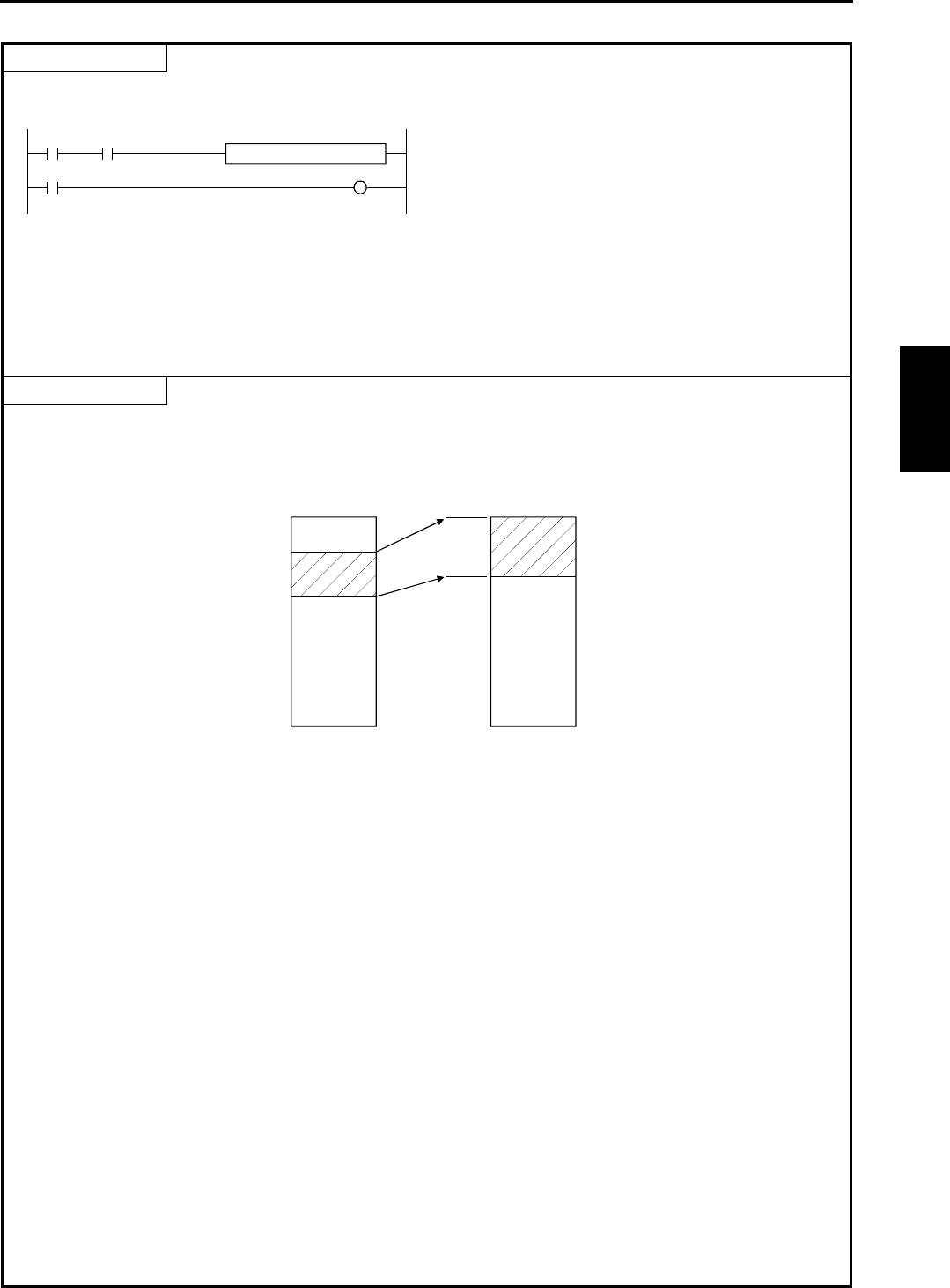
Chapter 5 Instruction Specifications
5-83
Program example
•The data in WM000 to WM01F is transferred to the area WR020 to WR03F.
R001 DIF0
R7F4
MOV
(
WR020,WM000,32
)
Y00100
SET
LD R001
AND DIF0
[
MOV
(
WR020,WM000,32
)
]
LD R7F4
SET Y00100
Program description
•32 words of data are transferred.
W
M000
W
M020
W
M03F
WR010
WR01F
Transfer source area Transfer destination area
MOV (d, s, n)
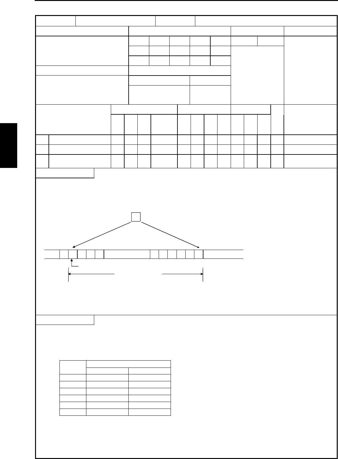
Chapter 5 Instruction Specifications
5-84
Item number Application instructions-13 Name Copy
Ladder format Condition code Processing time (µs) Remark
R7F4 R7F3 R7F2 R7F1 R7F0 Average Maximum
COPY (d, s, n) DER ERR SD V C
↕zzzz
Instruction format Number of steps
Condition Steps
As per the table
below.
COPY (d, s, n) 4
Bit Word Double word
Usable I/O XY
R,
M
TD, SS,
CU, CT WX WY
WR,
WM TC DX DY
DR,
DM
Constant
Other
d Copy destination head I/O {{
s Copy source head I/O {{{ {{{{ {
nNumber of bits (words)
to be copied {{{{ {
The constant is set in
decimal.
Function
•The value of s (bit, word) is copied from d to d + n - 1.
•The value of s is retained.
•A bit is copied to bits and a word is copied to words.
d+n-1 d
ssss
s
ssssss
n bits (words)
If n is a word: The contents (0 to 255) of the lower 8 bits (b7 to b0) of n (WX, WY, WR, WM, TC) are set to the
number of bits (words) to be copied.
If n is a constant: 0 to 255 (decimal) can be designated for the number of bits (words) to be copied.
Notes
•Use this instruction so that d + n - 1 does not exceed the I/O range (R7BF, M3FFF, WRFFF, and WM3FF). If it exceeds the
I/O range, DER is equal to '1' and transfers to the maximum range.
•If n is equal to “0,” the block copy is not be performed and DER (R7F4) will be set to “0.”
COPY (d, s, n)
Processing time (
µ
s) (Average)
nBit Word
180 73
16 83 114
32 83 148
64 88 224
128 95 381
255 109 785
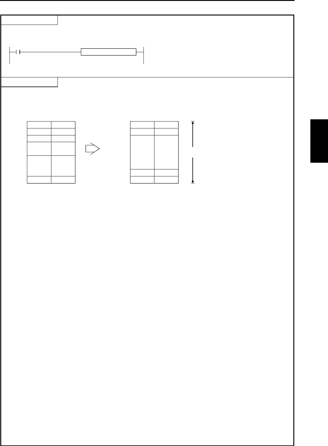
Chapter 5 Instruction Specifications
5-85
Program example
The default value (H2020) is set in the range of WR0100 to WR01FE.
R7E3 LD R7E3
[
COPY (WR0100, H2020, 255)
]
COPY (WR0100, H2020,255)
Program description
WR0100 to WR01FE is considered as the communication data area and is filled with space code (H20) as the default value
during the first scan after RUN starts.
R7E3: The first scan ON after RUN
WR0100
WR01FE
H20 H20
WR0100
WR01FE
H20 H20
H20 H20
H20 H20
Not fixed
After RUN
255 words
(510 bytes)
Not fixed
Not fixed Not fixed
•
•
•
•
•
•
•
•
•
•
•
•
•
•
•
•
COPY (d, s, n)

Chapter 5 Instruction Specifications
5-86
Item number Application instructions-14 Name Block exchange (EXCHANGE)
Ladder format Condition code Processing time (µs) Remark
R7F4 R7F3 R7F2 R7F1 R7F0 Average Maximum
XCG (d1, d2, n) DER ERR SD V C
↕zzzz
Instruction format Number of steps
Condition Steps
As per the table
below.
XCG (d1, d2, n) 4
Bit Word Double word
Usable I/O XY
R,
M
TD, SS,
CU, CT WX WY
WR,
WM TC DX DY
DR,
DM
Constant
Other
d1 Exchange destination
head I/O {{
d2 Exchange source head I/O {{
nNumber of bits (words)
to be exchanged {{{{ {
The constant is set in
decimal.
Function
•Exchanges the contents of the n bits from d1 to d1 + n - 1 and the contents between d2 and d2 + n - 1.
•Bits are exchanged with bits and words are exchanged with words.
d1+n-1
d2+n-1
d1
d2
n bits (words)
If n is a word: The contents (0 to 255) of the lower 8 bits (b7 to b0) of n (WX, WY, WR, WM, TC) are set to the
number of bits (words) to be exchanged.
If n is a constant: 0 to 255 (decimal) can be designated for the number of bits (words) to be exchanged.
Notes
•Use this instruction so that d1 + n − 1 and d2 + n - 1 do not exceed the I/O range (R7BF, M3FFF, WRFFF, and WM3FF). If they
exceeds the I/O range, DER is equal to '1' and the exchange is performed up to the maximum range with respect to the smaller number of
bits (words) specified in d1 and d2.
•If n is equal to “0,” the block exchange is not performed and DER (R7F4) will be set to “0.”
Program example
X00001 DIF1 XCG (WM000, WM100, 256)
LD X00001
AND DIF1
[
XCG (WM000, WM100, 256)
]
Program description
•When X00001 rises, the contents of WM000 to WM0FF are exchanged with the contents of WM100 to WM1FF.
XCG (d1, d2, n)
Processing time (
µ
s) (Average)
nBit Word
1 139 120
16 338 159
32 528 207
64 918 284
128 1899 449
255 3695 779
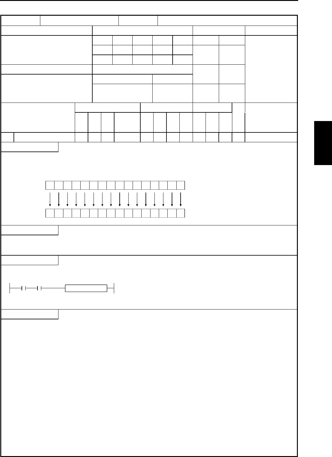
Chapter 5 Instruction Specifications
5-87
Item number Application instructions-15 Name NOT
Ladder format Condition code Processing time (µs) Remark
R7F4 R7F3 R7F2 R7F1 R7F0 Average Maximum
NOT (d) DER ERR SD V C Upper case: B
zzzzz 27
Instruction format Number of steps Middle case: W
Condition Steps 22
NOT (d) 2 Lower case: DW
28
Bit Word Double word
Usable I/O XY
R,
M
TD, SS,
CU, CT WX WY
WR,
WM TC DX DY
DR,
DM
Constant
Other
d I/O to be reversed {{ {{ {{
Function
•Reverses the contents of d.
1111000011110000
0000111100001111
Before execution
After execution
Notes
•Use edge trigger as the startup condition for this instruction.
Program example
R000 DIF0
LD R000
AND DIF0
[
NOT WR0000
]
NOT (WR0000)
Program description
•When R000 rises, the content of WR0000 is reversed.
Example) If WR0000 is H1234, WR0000 = HEDCB after the instruction is executed;
WR0000 = H1234 when executed again
NOT (d)
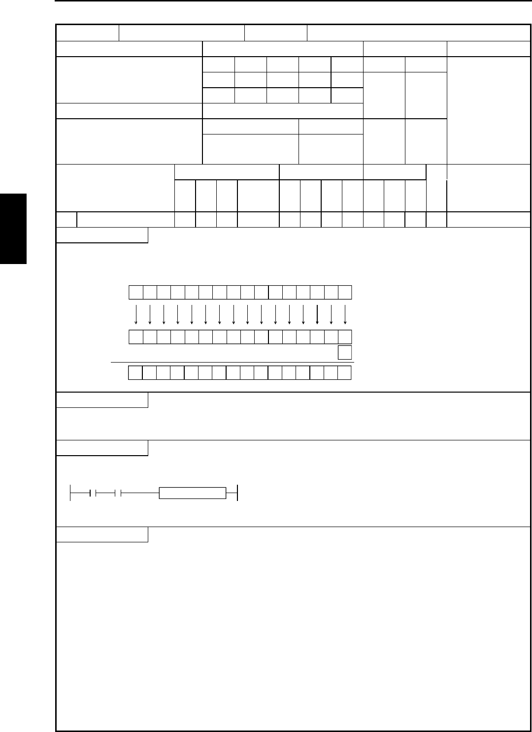
Chapter 5 Instruction Specifications
5-88
Item number Application instructions-16 Name Two's complement (NEGATE)
Ladder format Condition code Processing time (µs) Remark
R7F4 R7F3 R7F2 R7F1 R7F0 Average Maximum
NEG (d) DER ERR SD V C Upper case: W
zzzzz 22 Lower case: DW
Instruction format Number of steps
Condition Steps
NEG (d) 2 29
Bit Word Double word
Usable I/O XY
R,
M
TD, SS,
CU, CT WX WY
WR,
WM TC DX DY
DR,
DM
Constant
Other
d I/O to take complement {{ {{
Function
•Calculates two's complements of d (Reverses each bit contained in d and adds “1.” However, C (R7F0) remains
unchanged).
1100110000011010
0011001111100101
0011001111100110
1
Before execution
After execution
+
Notes
•Use edge trigger as the startup condition for this instruction.
Program example
LD R000
AND DIF0
[
NEG WR0000
]
NEG (WR0000)
R000 DIF0
Program description
•When R000 rises, 2's complement of the content of WR0000 is obtained.
Example) If WR0000 is H1234, WR0000 = HEDCC after the instruction is executed;
WR0000 = H1234 when executed again
NEG (d)
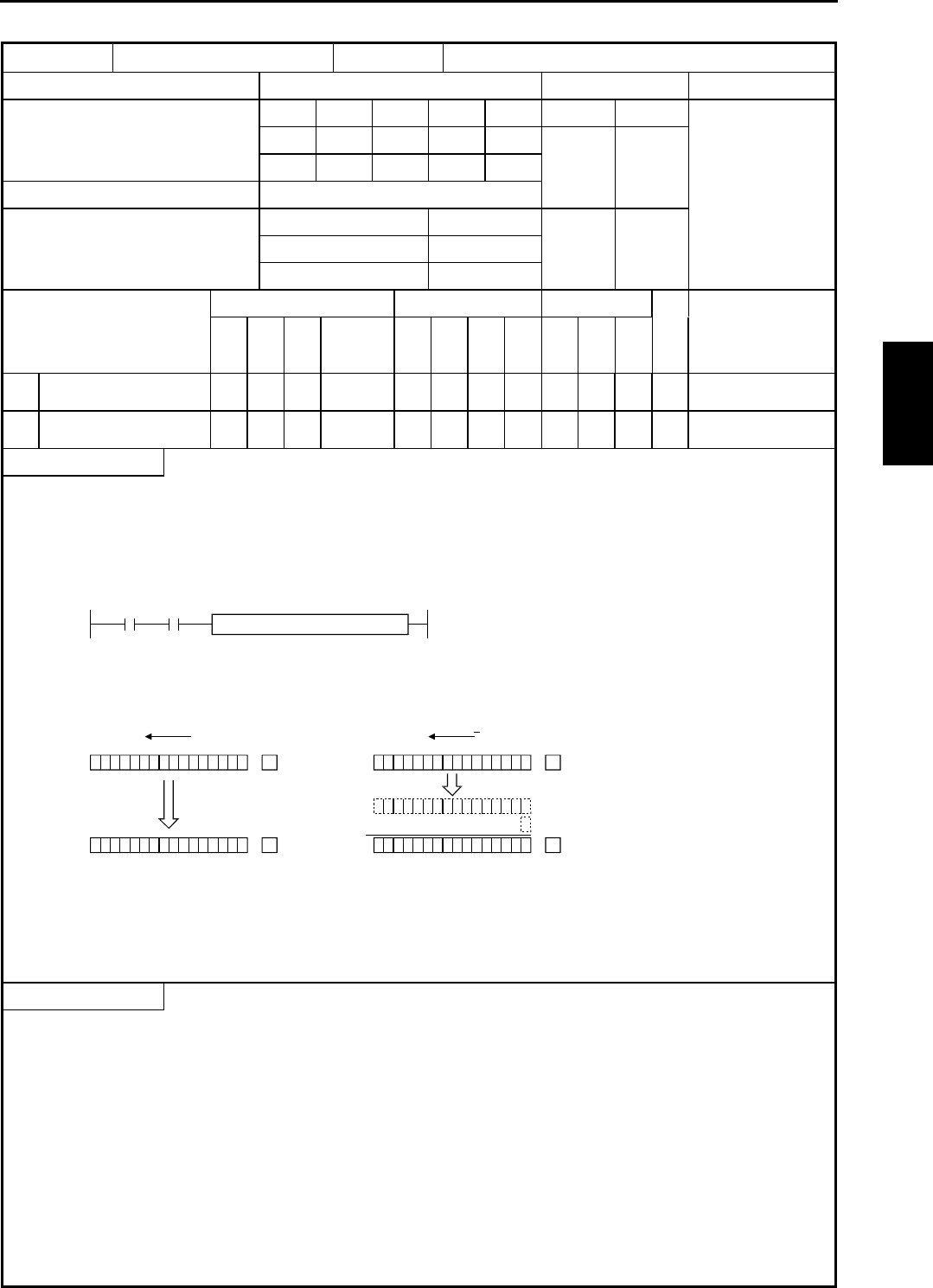
Chapter 5 Instruction Specifications
5-89
Item number Application instructions-17 Name Absolute value
Ladder format Condition code Processing time (µs) Remark
R7F4 R7F3 R7F2 R7F1 R7F0 Average Maximum
ABS (d, s) DER ERR SD V C Upper case: W
zzzz ↕30 Lower case: DW
Instruction format Number of steps
Condition Steps
ABS (d, s) Word 3 4
Double word 4
Bit Word Double word
Usable I/O XY
R,
M
TD, SS,
CU, CT WX WY
WR,
WM TC DX DY
DR,
DM
Constant
Other
dI/O after absolute value is
taken {{ {{
sI/O before absolute value
is taken {{{{{{{{
Function
•Given s is signed, set the absolute value of s in d.
•If s is positive or 0: The content of s is set to d. C (R7F0) is set to “0.”
•If s is negative: Two's complements of the contents of s are set in d. C (R7F0) is set to “1.”
•Perform with d and s as both words or both double words.
ABS
(
WR0000, WM0000
)
R000 DIF0
(When the value of WM is positive or 0)
WM0000 = H4C1A
0100110000011010WM0000
s
0
R7F0
d s
0100110000011010WR0000
d
0
(When the value of WM is negative)
WM0000 = HCC1A
1100110000011010WM0000
s
0
d s+1 R7F0
WR0000
d
1
0011001111100101
0011001111100110
1
+
Example:
•When s is a word: 0 to 32767 (decimal) correspond to H000 to H7FFF (hexadecimal).
−32768 to −1(decimal) correspond to H8000 to HFFFF (hexadecimal).
•When s is a double word: 0 to 2147483647 (decimal) correspond to H00000000 to H7FFFFFFF (hexadecimal).
−2147483648 to −1 (decimal) correspond to H80000000 to HFFFFFFFF (hexadecimal).
Notes
•Use edge trigger as the startup condition for this instruction.
ABS (d, s)
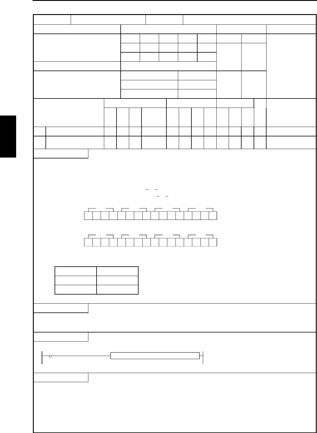
Chapter 5 Instruction Specifications
5-90
Item number Application instructions-18 Name Binary → BCD conversion
Ladder format Condition code Processing time (µs) Remark
R7F4 R7F3 R7F2 R7F1 R7F0 Average Maximum
BCD (d, s) DER ERR SD V C Upper case: W
↕zzzz 79 Lower case: DW
Instruction format Number of steps
Condition Steps
BCD (d, s) Word 3 89
Double word 4
Bit Word Double word
Usable I/O XY
R,
M
TD, SS,
CU, CT WX WY
WR,
WM TC DX DY
DR,
DM
Constant
Other
d I/O after conversion (BCD) {{ {{
sI/O before conversion
(BIN) {{{{{{{{
Function
•The result of the content conversion of s from binary to BCD is output to d.
•If the conversion result of s exceeds the number of BCD data digits in d, DER (R7F4) is set to '1' and the instruction will not
be executed.
If s is a word: set s so that H0000 ≤ s ≤ H270F (0 to 9999).
If s is a double word: set s so that H00000000 ≤ s ≤ H5F5E0FF (0 to 99999999).
0001101101001111
1B4F
0110100110010001
6991
1B4FH=6991
(BCD)
Before execution s
After execution d
(Binary)
Combinations of d and s.
ds
Word Word
Double word Double word
Notes
•If a data error occurred, the previous contents of d are retained.
Program example
X00000 BCD (WM0010, WR000 )
LD X00000
[
BCD
(
WM0010, WR000
)
]
Program description
•When X00000 turns on, the content of WR000 is converted from binary to BCD and output to WM0010.
WR000 H1B4F
After conversion
WM0010 H6691
BCD (d, s)

Chapter 5 Instruction Specifications
5-91
Item number Application instructions-19 Name BCD → Binary conversion
Ladder format Condition code Processing time (µs) Remark
R7F4 R7F3 R7F2 R7F1 R7F0 Average Maximum
BIN (d, s) DER ERR SD V C Upper case: W
↕zzzz 49 Lower case: DW
Instruction format Number of steps
Condition Steps
BIN (d, s) Word 3 75
Double word 4
Bit Word Double word
Usable I/O XY
R,
M
TD, SS,
CU, CT WX WY
WR,
WM TC DX DY
DR,
DM
Constant
Other
d I/O after conversion (BIN) {{ {{
sI/O before conversion
(BCD) {{{{{{{{
Function
•The result of the content conversion of s from BCD to binary is output to d.
•If the contents of s are not BCD data (if A through F is included in the data), DER (R7F4) is set to '1' and the conversion
will not be executed (d remains unchanged).
0110100110010001
6991
1B4F
(BCD)
0001101101001111
Before execution s
After execution d
(Binary)
Combinations of d and s.
ds
Word Word
Double word Double word
Notes
•If a data error occurred, the previous contents of d are retained.
Program example
X00000 BIN (WM0010, WR000 )
LD X00000
[
BIN
(
WM0010, WR000
)
]
Program description
•When X00000 turns on, the content of WR000 is converted from BCD to binary and output.
WR000 H6691
After conversion
WM0010 H1B4F
BIN (d, s)
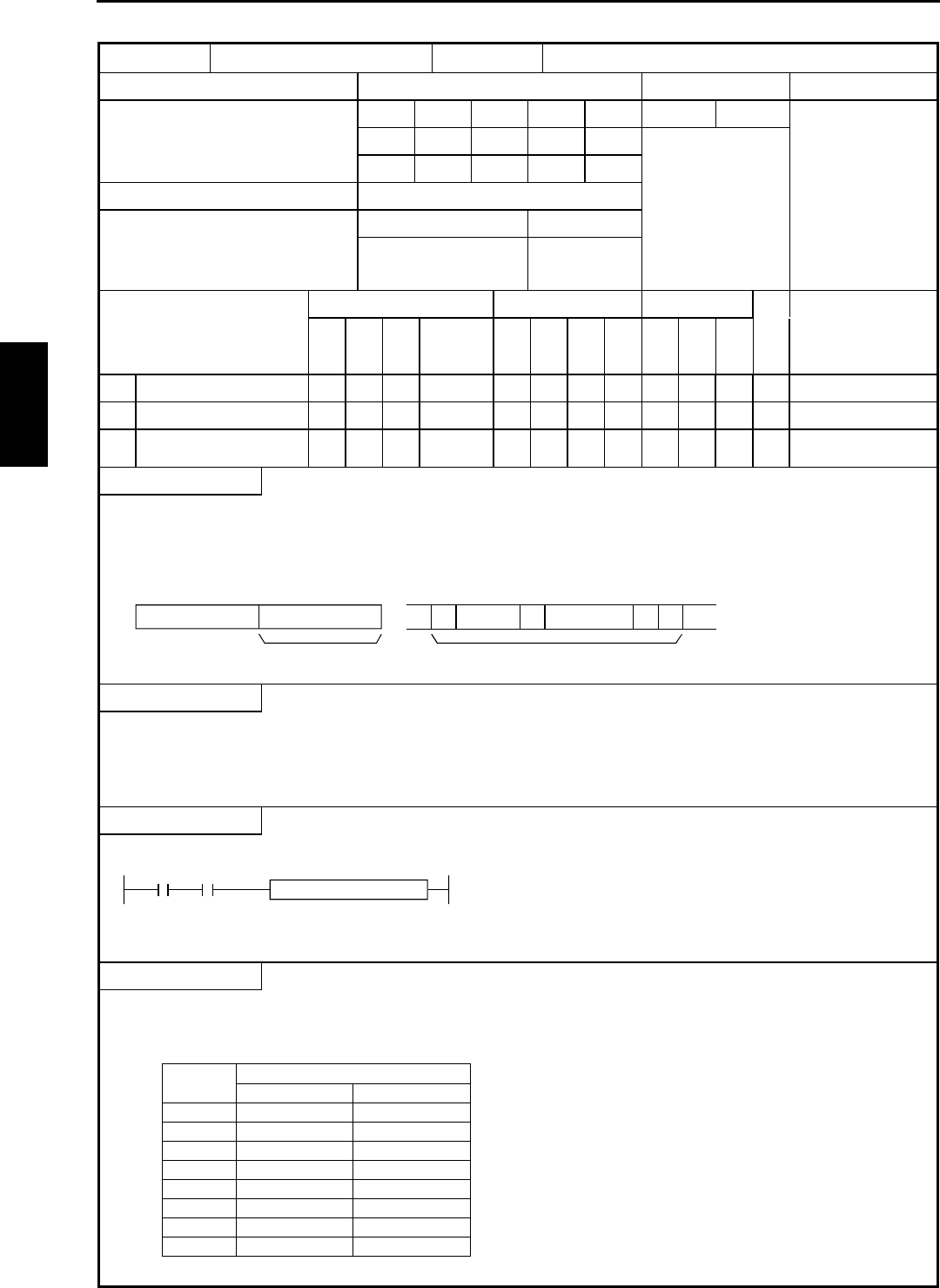
Chapter 5 Instruction Specifications
5-92
Item number Application instructions-20 Name Decode
Ladder format Condition code Processing time (µs) Remark
R7F4 R7F3 R7F2 R7F1 R7F0 Average Maximum
DECO (d, s, n) DER ERR SD V C
↕zzzz
Instruction format Number of steps
Condition Steps
As per the table
below.
DECO (d, s, n) 4
Bit Word Double word
Usable I/O XY
R,
M
TD, SS,
CU, CT WX WY
WR,
WM TC DX DY
DR,
DM
Constant
Other
dDecode destination head I/O {
s Word I/O to be decoded {{{{ {
nNumber of bits to be
decoded {1 to 8 (decimal)
Function
•Decodes the lower n bits of s to 2n and outputs '1' to the decoded bits in the bit rows between d and d + 2n – 1 (where n = 1
to 8). Note that the value “0” is output for bits other than the decoded bits in the bit row d + 2n – 1.
•If n is “0,” the instruction will not be executed, and the contents of d to d + 2n – 1 remain unchanged.
b15 b7 b0 d+2n-1 d+B
1
d
2n
s0BH 000
n bits (n = 1 to 8)
Notes
•Use this instruction so that d + 2n– 1 does not exceed the I/O range (R7BF and M3FFF). If it exceeds the I/O range, DER is
equal to '1' and the decoding is performed at the maximum range starting from d.
•Use 1 to 8 for n.
Program example
R100
LD R100
AND DIF1
[
DECO (R000, WX0000, 4)
]
DECO (R000, WX0000, 4)
DIF1
Program description
•When WX0000 = H000F, R00F, which is the 15th bit from R000 among the bits indicated by the lower four bit values of
WX0000, is set to “1” upon leading of R100.
DECO (d, s, n)
Processing time (µs)
nAverage Maximum
1 105 –
2 115 –
3 195 –
4 195 –
5 317 –
6 481 –
7 829 –
8 1586 –
Chapter 5 Instruction Specifications
5-93
Item number Application instructions-21 Name Encode
Ladder format Condition code Processing time (µs) Remark
R7F4 R7F3 R7F2 R7F1 R7F0 Average Maximum
ENCO (d, s, n) DER ERR SD V C
↕zzz ↕
Instruction format Number of steps
Condition Steps
As per the table
below.
ENCO (d, s, n) 4
Bit Word Double word
Usable I/O XY
R,
M
TD, SS,
CU, CT WX WY
WR,
WM TC DX DY
DR,
DM
Constant
Other
dDecode destination head I/O {{
s Word I/O to be encoded {
nNumber of bits to be
encoded {1 to 8 (decimal)
Function
•Encodes the bit location 2n in the range between s and s + 2n – 1 where the bit is “1,” and outputs the result to d (n = 1 to 8).
Upper bits (16-n) of d are set to “0.”
•If n is “0,” the instruction will not be executed and the contents of d retain the original values.
•If there are more than one bits that are set to “1” between s and s + 2n – 1, the upper bit location will be encoded.
•If all the bits from s to s + 2n – 1 are '0', '0' is output to d, and C (R7F0) is equal to '1.' In other cases, C (R7F0) is set to '0.'
b15 b7 b0s+2n-1 s+B
1
s
2n
000 0BH
d
n bits (1 to 8)
Notes
•Use this instruction so that s + 2n− 1 does not exceed the I/O range (R7BF and M3FFF). If it exceeds the I/O range, DER is
set to '1' and the encoding is performed at the maximum range starting from s.
•Use 1 to 8 for n.
Program example
X00001
LD X00001
AND DIF1
[
ENCO (WR0000, R000, 4)
]
ENCO (WR0000, R000, 4)
DIF1
Program description
•Upon the leading of X00001, the most significant bit that is set to “1” is detected within the row of bits R000 to R00F (24 –1
= 15 bits), and a four-bit binary number is set in the word I/O of d.
Example) If “1” is set in the 7th and 6th bits of R000 to R00F, H0007 is set in WR0000.
ENCO (d, s, n)
Processing time (µs)
nAverage Maximum
1 128 –
2 128 –
3 128 –
4 187 –
5 126 –
6 126 –
7 126 –
8 126 –
Chapter 5 Instruction Specifications
5-94
Item number Application instructions-22 Name Bit count
Ladder format Condition code Processing time (µs) Remark
R7F4 R7F3 R7F2 R7F1 R7F0 Average Maximum
BCU (d, s) DER ERR SD V C Upper case: W
zzzzz 33 Lower case: DW
Instruction format Number of steps
Condition Steps
BCU (d, s) Word 3 42
Double word 4
Bit Word Double word
Usable I/O XY
R,
M
TD, SS,
CU, CT WX WY
WR,
WM TC DX DY
DR,
DM
Constant
Other
d Number of bits set to 1 {{
sI/O that counts the bits
set to 1 {{{{{{{{
Function
•Of the contents of s (16 bits for word and 32 bits for double word), the number of bits that are set to “1” are output to d (0 to
32).
15 50
0 to 32
d11111 1111
15(32) 0
s• • •
Number of bits that are set to "1"
• • ••
• •• • •• • • • •• • •
Program example
X00002
LD X00002
AND DIF2
[
BCU (WR0000, DR0020)
]
BCU (WR0000, DR0020)
DIF2
Program description
•At the leading edge of X00002, the number of bits that are set to “1” among the data input to DR0020 is counted, and set to
WR0000.
Example)
10100111000101001111000101010011
DR0020 =
A 7 1 4 F 1 5 3
the number of bits set to "1" is 16 (decimal).
Therefore, the result is WR0000 = H0010.
In the case of
BCU (d, s)
Chapter 5 Instruction Specifications
5-95
Item number Application instructions-23 Name Swap
Ladder format Condition code Processing time (µs) Remark
R7F4 R7F3 R7F2 R7F1 R7F0 Average Maximum
SWAP (d) DER ERR SD V C
zzzzz
Instruction format Number of steps 25
Condition Steps
SWAP (d) 2
Bit Word Double word
Usable I/O XY
R,
M
TD, SS,
CU, CT WX WY
WR,
WM TC DX DY
DR,
DM
Constant
Other
d I/O to be exchanged {{
Function
•Swaps the upper 8 bits and lower 8 bits contained in d.
0001110101101101
0110110100011101
(Before execution) d
(After execution) d
Notes
•Use edge trigger as the startup condition for this instruction.
Program example
X00000 DIF0
SWAP (WR0010 )
LD X00000
AND DIF0
[
SWAP (WR0010)
]
Program description
•The upper and lower bits of WR0010 are swapped at the leading edge of X00000, and are stored in WR0010.
WR0010 H1234 Before execution
WR0010 H3412 After execution
Note: Since a scan is executed when there is no leading edge DIF0, the upper and lower bits of WR0010 are swapped every
time a scan is executed.
SWAP (d)
Chapter 5 Instruction Specifications
5-96
Item number Application instructions-24 Name Unit
Ladder format Condition code Processing time (µs) Remark
R7F4 R7F3 R7F2 R7F1 R7F0 Average Maximum
UNIT (d, s, n) DER ERR SD V C
↕zzzz
Instruction format Number of steps
Condition Steps
As per the table
below.
UNIT (d, s, n) 4
Bit Word Double word
Usable I/O XY
R,
M
TD, SS,
CU, CT WX WY
WR,
WM TC DX DY
DR,
DM
Constant
Other
dUnity result write
destination I/O {{
s Unity destination head I/O {
nNumbers of words to be
united {n=0 to 4
Function
•Sets the values in the lower four bits of each of the n (1 to 4) words starting from s to the lower four bits of each word in d.
•If n is 1 to 3, the bits not set in d will be “0.”
•The data stored in s to s + n – 1 will be retained even if UNIT is executed.
•Use this instruction so that s + n - 1 does not exceed the I/O range (WRFFF and WM3FF). If it exceeds the I/O range, DER
is equal to '1' and the lower four bits within the range between s and I/O will be set in d.
s
s+1
s+2
s+3
B1
B2
B3
B4
B4 B3 B2 B1
d
When n is 1 : B2 to B4 of d are 0
When n is 2 : B3 to B4 of d are 0
When n is 3 : B4 of d is 0
W
hen n=4
Upper digits Lower digits
4 bits
Ignored
Notes
•When n=0, it is not executed.
•When n>5, it is not executed.
UNIT (d, s, n)
Processing time (µs)
nAverage Maximum
075 –
1 100 –
2 103 –
3 106 –
4 109 –

Chapter 5 Instruction Specifications
5-97
Program example
X00001
LD X00001
AND DIF0
[
UNIT
(
WY0010, WR0000, 3
)
]
UNIT
(
WY0010, WR0000, 3
)
DIF0
Program description
A 3-digit BCD input display device is connected to the WY0010, and each digit displays WR0000 to WR0002 data
independently. (Only the lower four bits are considered the valid data for WR0000 to WR0002.)
3 2 7
Y111 to Y108 Y107 to Y104 Y103 to Y100
Line No. Conveyor No. Product No.
3-digit BCD input display device
WR0002
(Line No.)
WR0001
(
Conve
y
or No.
)
WR0000
(Product No.)
Data “3”
Data “2”
Data “7”
28-point type
Output
Input
UNIT (d, s, n)
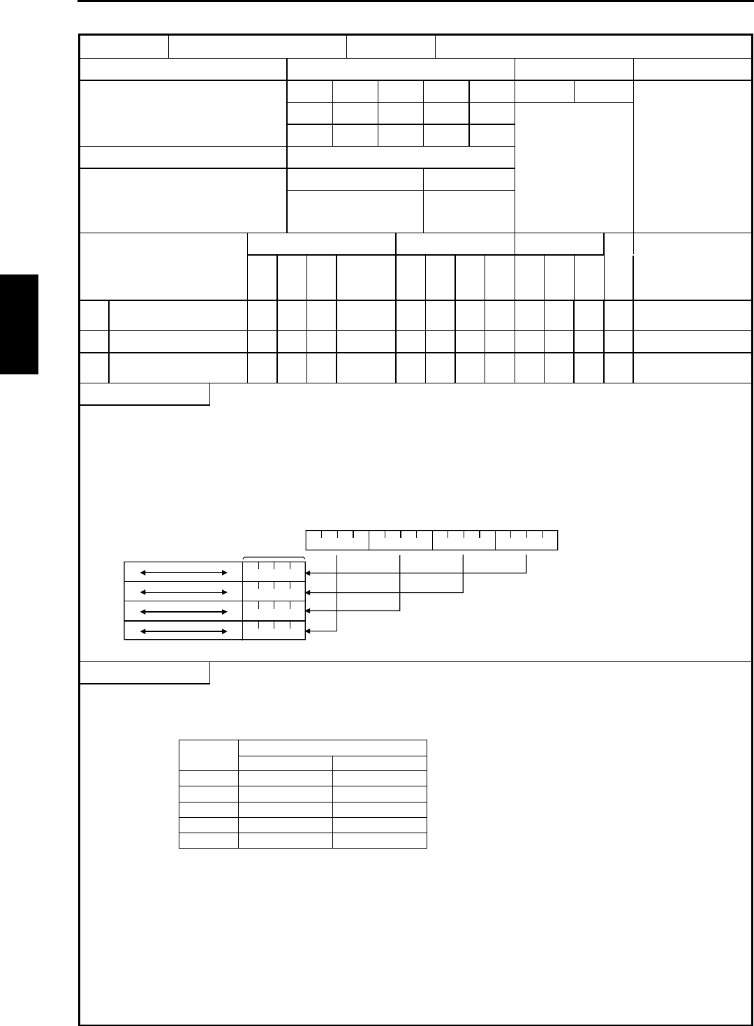
Chapter 5 Instruction Specifications
5-98
Item number Application instructions-25 Name Distribute
Ladder format Condition code Processing time (µs) Remark
R7F4 R7F3 R7F2 R7F1 R7F0 Average Maximum
DIST (d, s, n) DER ERR SD V C
↕zzzz
Instruction format Number of steps
Condition Steps
As per the table
below.
DIST (d, s, n) 4
Bit Word Double word
Usable I/O XY
R,
M
TD, SS,
CU, CT WX WY
WR,
WM TC DX DY
DR,
DM
Constant
Other
dDistribution result write
destination head I/O {
s I/O to be distributed {{{{ {
nNumber of words to be
distributed {n=0 to 4
Function
•Distributes s into four bit sections and sets to the lower four bits of the n words starting from d.
•The upper 12 bits of the range d to d + n – 1 will be “0.”
•The value of s will be retained even if DIST is executed.
•Use this instruction so that d + n - 1 does not exceed the I/O range (WRFFF and WM3FF). If it exceeds the I/O range, DER
is equal to '1' and the distribution data for s will be set in the lower four bits within the range between d and the I/O.
d
d+1
d+2
d+3
B1
B2
B3
B4
B4 B3 B2 B1
00
00
00
00
s
4 bits
Upper digits Lower digits
When n = 4:
Notes
•When n=0, it is not executed.
DIST (d, s, n)
Processing time (µs)
nAverage Maximum
062 –
187 –
290 –
392 –
494 –
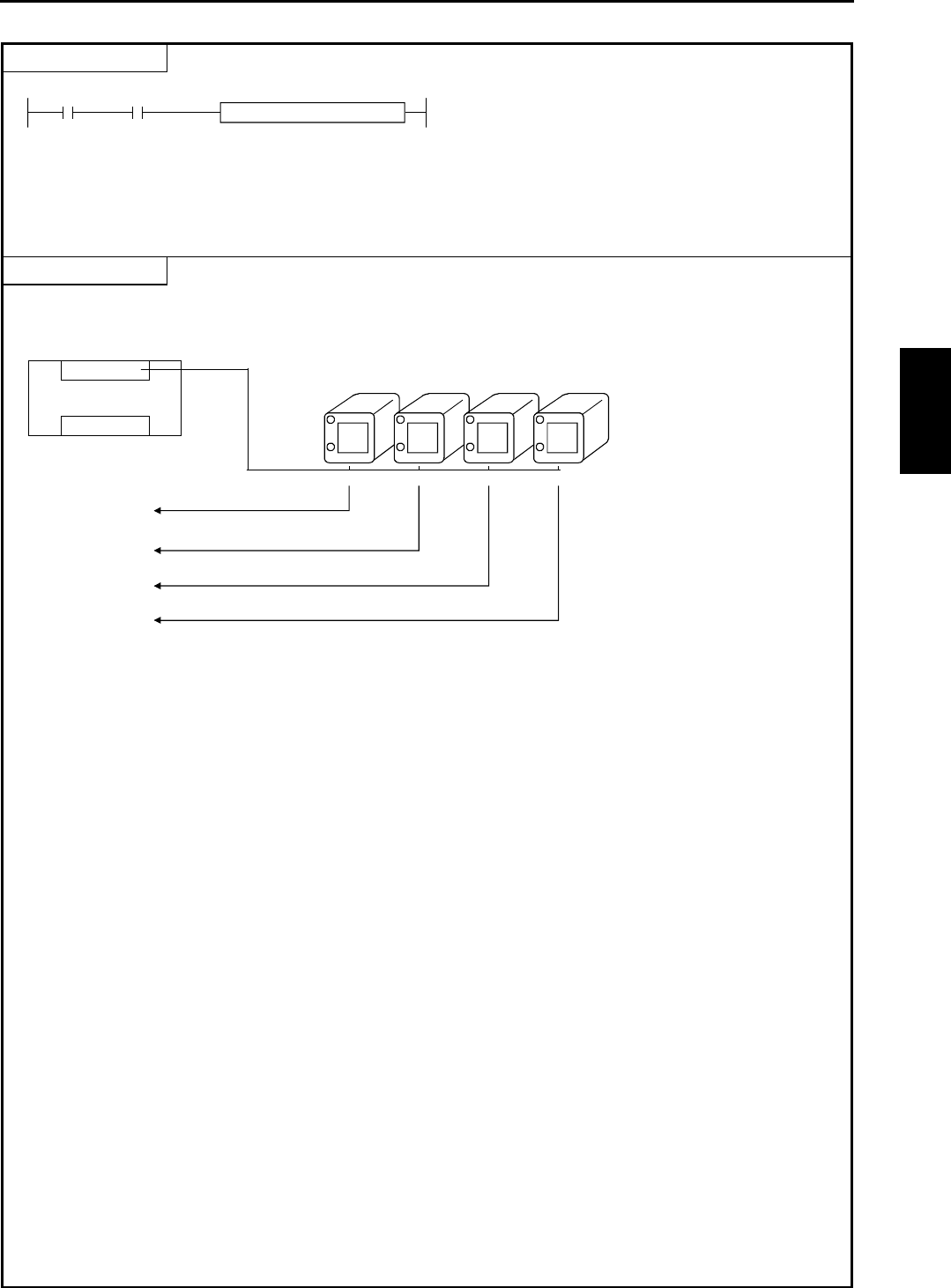
Chapter 5 Instruction Specifications
5-99
Program example
X01001
LD X00001
A
ND DIF0
[
D
IST (WR0000, WX0000, 4)
]
DIST (WR0000, WX0000, 4)
DIF0
Program description
A 4-bit 4-digit Digit switch is connected to the WX0000, and the data for each digit is stored in WR0000 to WR0003 as
independent data.
9 7 4 6
X015 to X012 X011 to X008 X007 to X004 X003 to X000
WR0003
=H0009
WR0002
=H0007
WR0001
=H0004
WR0000
=H0006
28-point type
Output
Input
DIST (d, s, n)
Chapter 5 Instruction Specifications
5-100
Item number Control instructions-1 Name Normal scan end
Ladder format Condition code Processing time (µs) Remark
R7F4 R7F3 R7F2 R7F1 R7F0 Average Maximum
END DER ERR SD V C
zzzzz
Instruction format Number of steps 714
Condition Steps
END 1
Bit Word Double word
Usable I/O XY
R,
M
TD, SS,
CU, CT WX WY
WR,
WM TC DX DY
DR,
DM
Constant
Other
Function
•Indicates the end of a normal scan program. (The execution of this instruction returns to the beginning of the program, and
a normal scan is executed.)
•This instruction is not required when there are no subroutine programs or interrupt scan programs.
•If there is a subroutine program or interrupting program, write this instruction at the end of the normal scan program.
•This instruction is used only once in a program. Do not use any startup conditions with this instruction.
Notes
•The END instruction is checked prior to the execution, and if there is an error, the following error codes are set in the special
internal output WRF001. Also, the CPU error code '34' is set to special internal output WRF000.
CPU error code Special internal output Error code Error description
H0010 There is no END instruction.
34 WRF001 H0022 There are two or more END instructions.
H0032 A startup condition is used with the END
instruction.
Instruction for use
END
SB n
INT n
END instruction
Normal scan program
Subroutine program
Interrupt program
END
Chapter 5 Instruction Specifications
5-101
Item number Control instructions-2 Name Scan conditional end
Ladder format Condition code Processing time (µs) Remark
R7F4 R7F3 R7F2 R7F1 R7F0 Average Maximum
CEND (s) DER ERR SD V C Upper case :
zzzzz 5Conditions
Instruction format Number of steps do not meet
Condition Steps Lower case :
CEND (s) 2 707 Conditions meet
Bit Word Double word
Usable I/O XY
R,
M
TD, SS,
CU, CT WX WY
WR,
WM TC DX DY
DR,
DM
Constant
Other
s Scan end condition {{{
Function
•If the scan end condition (s) is on, the execution of this instruction returns to the head of the scan program and executes the
program.
•If (s) is off, the next instruction is executed.
•This instruction can only be used in normal scan programs, and can be used as many times as desired.
•This instruction can specify a startup condition. In this case, if the startup condition and (s) are both on, this instruction is
executed.
Notes
•The CEND instruction is checked prior to the execution, and if there is an error, the following error codes are set in the
special internal output WRF001. Also, the CPU error code '34' is set to special internal output WRF000.
CPU error code Special internal output Error code Error description
34 WRF001 H0023 The CEND instruction is found after the END
instruction.
Instruction for use
CEND (R000)
CEND (R001)
END
Program head
Normal scan program
Normal scan program
Normal scan program
When R000 is on, to
program head
When R000 is off, the next
instruction is executed.
When R001 is on, to
program
When R001 is off, the next
instruction is executed.
CEND (s)
Chapter 5 Instruction Specifications
5-102
Item number Control instructions-3 Name Unconditional jump (JUMP)
Ladder format Condition code Processing time (µs) Remark
R7F4 R7F3 R7F2 R7F1 R7F0 Average Maximum
JMP n DER ERR SD V C
z1] zzz
Instruction format Number of steps 32
Condition Steps
JMP n 2
Bit Word Double word
Usable I/O XY
R,
M
TD, SS,
CU, CT WX WY
WR,
WM TC DX DY
DR,
DM
Constant
Other
n Code number {0 to 255 (Decimal)
Function
•If the startup condition of JMP n switches on, the control jumps the program from this instruction to the LBL n of the same
code number. Always use JMP n and LBL n in pairs.
•If the startup condition is not established, the next instruction will be executed.
•To set this instruction in conjunction with other instructions in the same arithmetic-operation box, insert this instruction at
the end of the box.
•The JMP n instruction is valid only within the same scan program. (A jump to a subroutine or interrupt scan cannot be
performed from a normal scan, nor vice versa.)
•Nesting of JMP n instructions is possible, but note so that an overload error does not occur.
Notes
•This instruction is checked prior to the execution, and if there is an error, the following error codes are set in the special
internal outputs R7F3 and WRF015. In this case, jump is not performed and the next instruction will be executed.
Special internal output Error code Error description
R7F3=1 WRF015 H0015 There is no LBL n.
H0040 A jump is attempted to a different program area.
Instruction for use
JMP n
LBL n
Program
Program
•When the startup condition turns on, it jumps to LBL n.
•If there is a timer within the program it jumped to, the progress value is updated,
but since instructions are not executed, output will not be turned on even if the
ON conditions are met.
JMP n
Chapter 5 Instruction Specifications
5-103
Item number Control instructions-4 Name Conditional jump
Ladder format Condition code Processing time (µs) Remark
R7F4 R7F3 R7F2 R7F1 R7F0 Average Maximum
CJMP n (s) DER ERR SD V C Upper case :
z1] zzz 3Conditions
Instruction format Number of steps do not meet
Condition Steps Lower case :
CJMP n (s) 3 32 Conditions meet
Bit Word Double word
Usable I/O XY
R,
M
TD, SS,
CU, CT WX WY
WR,
WM TC DX DY
DR,
DM
Constant
Other
nCode number {0 to 255 (Decimal)
sJump condition {{{
Function
•If the jump condition (s) of CJMP n(s) switches on, the control jumps the program from this instruction to the LBL n of the
same code number. Always use CJMP n(s) and LBL n in pairs.
•If the startup or jump condition is not established, the next instruction will be executed.
•To set this instruction in conjunction with other instructions in the same arithmetic-operation box, caution must be used
because the jump takes place without performing the operations specified after the instruction.
•The CJMP n(s) instruction is valid only within the same scan program. (A jump to a subroutine or interrupt scan cannot be
performed from a normal scan, nor vice versa.)
•Nesting of CJMP n(s) instructions is possible, but note so that an overload error does not occur.
Notes
•This instruction is checked prior to the execution, and if there is an error, the following error codes are set in the special
internal outputs R7F3 and WRF015. In this case, jump is not performed and the next instruction will be executed.
Special internal output Error code Error description
R7F3=1 WRF015 H0015 There is no LBL n.
H0040 A jump is attempted to a different program area.
Instruction for use
Program
?????
Program
LBL n
CJMP n (R000)
R101 •When the startup condition and the R000 jump condition bit I/O are both on, it
jumps to LBL n.
•If there is a timer within the program it jumped to, the progress value is updated,
but since instructions are not executed, output will not be turned on even if the
ON conditions are met.
CJMP n (s)
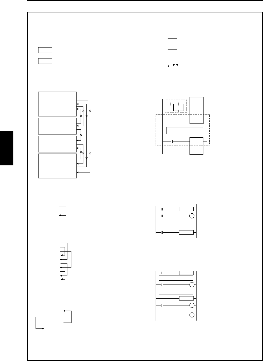
Chapter 5 Instruction Specifications
5-104
Syntax of JMP, CJMP
LBL 2
JMP 1
JMP 1
LBL 7
JMP 2
LBL 3
END
SB
JMP 3
LBL 2
JMP 4
RTS
SB
LBL 4
JMP 5
LBL 6
PTS
INTO
JMP 6
LBL 5
JMP 7
LBL 1
RTI
JMP 5
A]
B] LBL 5
LBL 5
JMP 0
JMP 1
JMP 2
LBL 1
LBL 0
JMP 3
LBL 2
JMP 4
LBL 3
LBL 4
LBL 0
CJMP1(X00000)
JMP 0
LBL 1
JMP 5
JMP 5
CJMP 5
LBL 5
JMP 0
Program A
Program C
Program B
X00000 X00001
X00002
X00003
LBL 0
X00000
X00001
JMP 1
LBL 1
TD0
0.1s
100
X00000
X00001
JMP 1
MCS0
LBL 2
X00002 Y00100
MCR0
Program
Program
1] LBL n with the same code number as the code
number n of the JMP instruction is required.
• If JMP 1 is executed when there
is no LBL 1, an LBL undefined
error occurs. JMP 1 will do
nothing and execute the next
processing of program A.
6] An overlap of JMP instructions with the same code
number is valid.
Program A
Program B
2] Jump is not permitted to outside the area in which the JMP
instruction resides. 7] A startup condition can be programmed with respect to
JMP instructions.
•When the JMP 1 instruction
is executed, since LBL 1 is
not in the normal scan area,
a "jump outside the area"
error will be generated. The
JMP 1 instruction will do
nothing and execute the next
processing of program.
•JMP 2 to JMP 7 perform
similar processing.
•If a jump is performed
from JMP 0 to LBL 0,
programs A, B and C
will not be executed.
3] Code number n of the JMP instruction and the LBL n with
the same code number may not be overlapped.
8] The CJMP instruction also follows the same syntax as 1]
through 7].
Note 1: When a JMP instruction jumps to LBL, the status
of each I/O between JMP and LBL is retained.
However, the timer progress value will be updated.
•In the pre-operation process, the
label instructions A] and B] have 5
as the code numbers, so a duplicate
definition error will occur.
•If X00000 turns on after
X00001 turns on, the
progress value of TD0 will
be updated even if a jump
is performed from JMP 1
to LBL 1. If X00000
remains on, TD0 will not
turn on even if its progress
value exceeds 100.
4] Nesting of JMP instructions is allowed.
5] The JMP instruction can jump to a location before the
instruction itself.
Note 2: If the JMP instruction is used in conjunction with
the MCS or MCR instruction, the following actions
will result, so exercise caution when programming.
Note 3: Do not create a circuit that jumps to outside from
between MCS and MCR.
•When JMP 2 does not
jump, Y00100 will turn on
when X00001 and X00002
are both on.
•When JMP 2 does jump, if
X00000 is on, Y00100 will
follow the on/off of
X00002 regardless of the
on/off of X00001.
•JMP 0 will jump to LBL 0, which is a
location before the JMP instruction.
•When input X00000 turns on, the loop
between LBL 0 and JMP 0 is escaped
by jumping from CJMP 1 (X00000) to
LBL 1.
•If there is no instruction as CJMP 1
(X00000) to escape from the loop, the
loop from LBL 0 to JMP 0 will
continue endlessly.
Program head
Normal scan area
Subroutine area
Subroutine area
Interrupt scan area
Startup condition
CJMP n (s)
Chapter 5 Instruction Specifications
5-105
Item number Control instructions-5 Name Label
Ladder format Condition code Processing time (µs) Remark
R7F4 R7F3 R7F2 R7F1 R7F0 Average Maximum
LBL n DER ERR SD V C
zzzzz
Instruction format Number of steps 0.5
Condition Steps
LBL n 1
Bit Word Double word
Usable I/O XY
R,
M
TD, SS,
CU, CT WX WY
WR,
WM TC DX DY
DR,
DM
Constant
Other
n Code number {0 to 255 (Decimal)
Function
•This instruction indicates the destination of the jump when the JMP n or CJMP n instruction is executed (n is always used in
pairs).
•The n in the LBL n cannot be used multiple times in the same program.
•This instruction itself does not perform any operation.
•Even if a startup condition is used with LBL n, it will be ignored.
Notes
•This instruction is checked prior to execution, and when there is an error, the following error code is set in the special
internal output WRF001. Also, the CPU error code '34' is set to special internal output WRF000.
CPU error code Special internal output Error code Error description
34 WRF001 H0001 Duplicate definition of LBL
Instruction for use
R100 (00001)
(00002)
(00003)
JMP 0
WR0000 = WR0000 + 1
LBL 0
R100 (00004)
(00005)
(00006)
WR0000 = WR0000 - 1
LBL 1
JMP 1
•When R100 is on, JMP 0 will be executed but JMP 1 will not be executed.
Therefore, the content of WR0000 will decrement by one during each scan.
•When R100 is off, JMP 0 will not be executed but JMP 1 will be executed.
Therefore, the content of WR0000 will increment by one during each scan.
LBL n
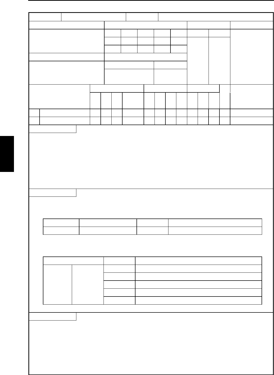
Chapter 5 Instruction Specifications
5-106
Item number Control instructions-6 Name FOR
Ladder format Condition code Processing time (µs) Remark
R7F4 R7F3 R7F2 R7F1 R7F0 Average Maximum
FOR n (s) DER ERR SD V C
z1] zzz
Instruction format Number of steps 33
Condition Steps
FOR n (s) 3
Bit Word Double word
Usable I/O XY
R,
M
TD, SS,
CU, CT WX WY
WR,
WM TC DX DY
DR,
DM
Constant
Other
n Code number {0 to 49 (Decimal)
sNumber of times repeated {{
Function
•Jumps from the NEXT n of the same code number to this instruction.
•If the number of times repeated (s) is greater than 0, the instruction following the FOR n (s) is executed.
•If the number of times repeated (s) is equal to 0, it jumps to the instruction following the NEXT n.
•Use FOR n (s) and NEXT n in pairs. Also, place the NEXT n after FOR n.
•The FOR n (s) may not be used more than once.
•Use the FOR n (s) and NEXT n in the same program area. (It is not allowed to include FOR n (s) in the normal scan and
NEXT n in the subroutine area.)
•The FOR n (s) to NEXT n nesting can be made up to five levels.
Notes
•This instruction is checked prior to execution, and when there is an error, the following error code is set in the special
internal output WRF001. Also, the CPU error code '34' is set to special internal output WRF000.
CPU error code Special internal output Error code Error description
34 WRF001 H0001 Duplicate definition of FOR
•If an error is generated during the execution of the instruction, an error code will be set in the special internal outputs R7F3
and WRF015, and the following program will be executed.
Special internal output Error code Error description
H0017 NEXT undefined
H0043 FOR to NEXT error
R7F3=1 WRF015 H0044 Area error for NEXT
H0045 FOR to NEXT nesting error
H0046 FOR nesting overflow
Instruction for use
•For the instruction instruction, see NEXT n.
FOR n (s)
Chapter 5 Instruction Specifications
5-107
Item number Control instructions-7 Name NEXT
Ladder format Condition code Processing time (µs) Remark
R7F4 R7F3 R7F2 R7F1 R7F0 Average Maximum
NEXT n DER ERR SD V C
z1] zzz
Instruction format Number of steps 38
Condition Steps
NEXT n 2
Bit Word Double word
Usable I/O XY
R,
M
TD, SS,
CU, CT WX WY
WR,
WM TC DX DY
DR,
DM
Constant
Other
n Code number {0 to 49 (Decimal)
Function
•Subtracts 1 from the number of times repeated (s) for the FORn (s) instruction of the same code number, then jumps to
FORn (s).
Notes
•This instruction is checked prior to execution, and when there is an error, the following error code is set in the special
internal output WRF001. Also, the CPU error code '34' is set to special internal output WRF000.
CPU error code Special internal output Error code Error description
34 WRF001 H0003 Duplicate definition of NEXT
•If an error is generated during the execution of the instruction, an error code will be set in the special internal outputs R7F3
and WRF015, and the following program will be executed.
Special internal output Error code Error description
R7F3=1 WRF015 H0016 FOR undefined
H0046 FOR nesting overflow
Instruction for use
When
WR0000 > 0
When
WR0000 = 0
WR0000 = 512
WR0001 = 0
FOR 0(WR0000)
TC0(WR0001) = 0
WR0001 = WR0001 + 1
NEXT 0
R000 DIF0
To the next program
•When R000 is turned on, the progress value (TC n) of the timer or counter is
cleared with 0 for 512 points.
•Once the FOR to NEXT starts, the instruction keeps executing until (s) is “0.”
•FOR0 (WR0000) performs instructions after TC0 (WR0001) = 0 while
WR0000>0, subtracts “1” from WR0000 at NEXT0, then jumps to FOR0
(WR0000).
•FOR0 (WR0000) jumps to the next instruction within the current box upon
WR0000 = 0.
NEXT n
Chapter 5 Instruction Specifications
5-108
Syntax of FOR to NEXT
FOR 1 (WR0010)
NEXT 2
NEXT 5
FOR 5 (WM04F)
Program
Program
Program
Program
Program
NEXT 3
FOR 3
Program
Program
Program
FOR 3 (WR10)
NEXT 3
SB1
NEXT 2
FOR 3(WR0003)
RTS
SB2
NEXT 3
FOR 4(WR0004)
RTS
INT0
NEXT 4
NEXT 1
RT1
FOR 1(WR0001)
FOR 2(WR0002)
END
FOR3
Program
FOR 1 (WM001)
NEXT 1
Program
Program
FOR 2 (WM002)
NEXT 2
FOR 1 (WM001)
CJMP 10 (X00000)
NEXT 1
LBL10
FOR 1(WR0001)
FOR 2(WR0002)
FOR 3(WR0003)
FOR 4(WR0004)
FOR 5(WR0005)
FOR 6(WR0006)
NEXT 6
NEXT 5
NEXT 4
NEXT 3
NEXT 2
NEXT 1
X00000 JMP 1
FOR 1(WM001)
NEXT 1
LBL 1
Program C
WR0010=1
WR0010=20
FOR 1(WR0010)
Program A
NEXT1
R005
Program B
FOR 1(WM001) to NEXT 1 will execute
normally.
•Nesting error
When WM002=0
Since FOR 1(WM001) to NEXT 1 is
prioritized, jump will not be performed
over NEXT 1 from FOR 2 to NEXT 2.
At this time, NEXT 2 generates a FOR
2 undefined error.
When WM002 ≠ 0
FOR 2 will not do anything. Therefore,
NEXT 2 will generate a FOR 2
undefined error.
•When R005 is off
Program B is executed after program A is repeated 20
times.
•When R005 is on
The repeat counter WR0010 changes to 1, and since the
NEXT 1 processing subtracts 1 from it, the content of
WR0010 becomes 0. Therefore, the repeating of
program A is terminated and program B is execute
4] Use FOR to NEXT as a nest.
8] The number of repeats may be modified within the
program.
The content of WR0010
decrements by 1 and a jump is
performed to FOR 1 (WR0010).
1] A NEXT instruction with the same code number as the
code number n of the FOR instruction is required after
the FOR instruction.
5] It is possible to escape from a FOR to NEXT loop
using a jump instruction.
•NEXT undefined error
The NEXT instruction with
respect to the FOR instruction
does not exist within the user
program.
•FOR undefined error
The FOR instruction does not exist
before the NEXT instruction.
•NEXT to FOR error
The NEXT instruction exists
before the FOR instruction.
The FOR 1 to NEXT 1 loop is
escaped when X00000 turns on
before the loop has been repeated
for the set number of repeats
(content of WM001).
2] An overlap of FOR and NEXT instructions with the
same code number n is not allowed.
6] FOR to NEXT may be nested up to 5 levels. When a
subroutine is included, the FOR to NEXT within the
subroutine is counted.
•Nesting overflow error
•FOR duplicate-definition error
A FOR instruction with the same
code number n is programmed.
•NEXT duplicate-definition error
A NEXT instruction with the same
code number n is programmed.
Note: FOR and NEXT duplicate-
definition errors will occur
during operation pre-processing.
3] FOR and NEXT must be within the same area.
7] Do not include a startup condition between FOR and
NEXT. If a startup condition is required, create a
circuit as shown below:
Program head
Normal scan
Subroutine
SB1
Subroutine
SB2
Interrupt scan
[Operation description]
When X00000 is off, program C is
repeatedly executed for the
number of WM 1 times.
When X00000 is on, program C is
not executed since a jump is
performed from JMP 1 to LBL 1.
NEXT n
Chapter 5 Instruction Specifications
5-109
Item number Control instructions-8 Name Call subroutine
Ladder format Condition code Processing time (µs) Remark
R7F4 R7F3 R7F2 R7F1 R7F0 Average Maximum
CAL n DER ERR SD V C
z1] zzz
Instruction format Number of steps 24
Condition Steps
CAL n 2
Bit Word Double word
Usable I/O XY
R,
M
TD, SS,
CU, CT WX WY
WR,
WM TC DX DY
DR,
DM
Constant
Other
n Code number {0 to 99 (Decimal)
Function
•If the startup condition of CAL n is on, this instructions executes the subroutine program (the program sandwiched by SB n and
RTS) of the same code number.
•If the startup condition is off, the next program is executed.
•Up to 5 levels of CAL (nesting) for another subroutine can be performed within a subroutine.
•It is possible to call a subroutine from within an interrupt scan program.
Notes
•If an error is generated during the execution of the instruction, an error code will be set in the special internal outputs R7F3 and
WRF015, and the following program will be executed.
Special internal output Error code Error description
R7F3=1 WRF015 H0013 SB undefined
H0041 Nesting error
Instruction for use
R000
CAL n
SB n
RTS
END
Other program
Subroutine program
R000 turns
ON
R000 turns
OFF
•When R000 is on, a subroutine program is executed by CAL n. After
the execution, the program is re-executed from the code following the
CAL n.
•When R000 is off, the subroutine program is not executed, and the
next program is executed.
CAL n
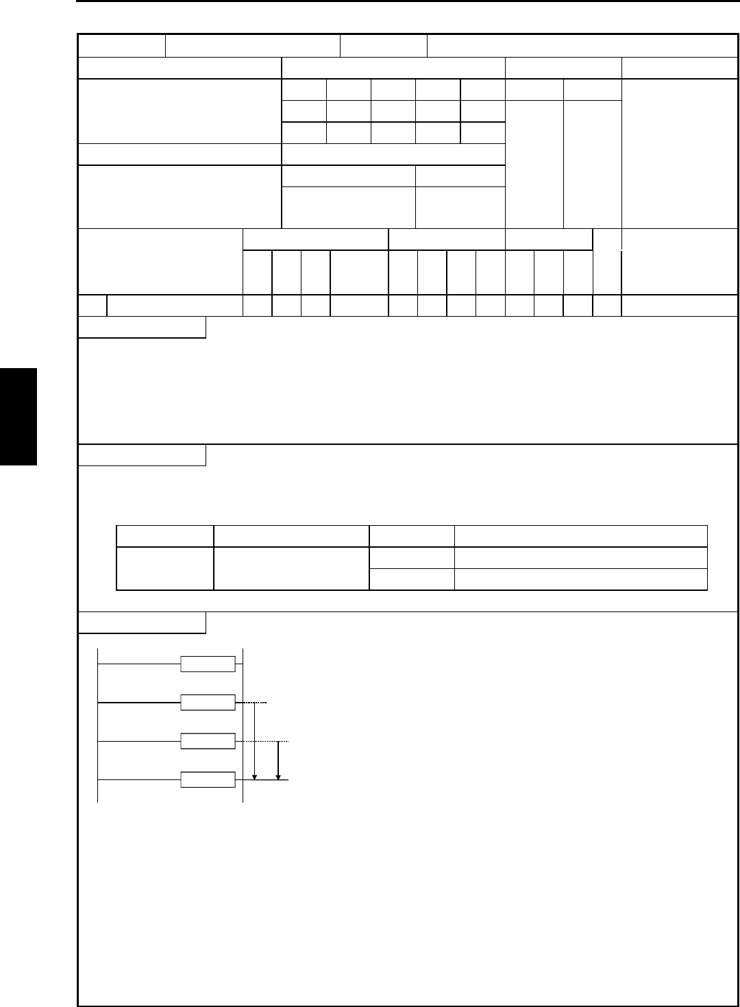
Chapter 5 Instruction Specifications
5-110
Item number Control instructions-9 Name Start subroutine program
Ladder format Condition code Processing time (µs) Remark
R7F4 R7F3 R7F2 R7F1 R7F0 Average Maximum
SB n DER ERR SD V C
z1] zzz
Instruction format Number of steps 0.5
Condition Steps
SB n 1
Bit Word Double word
Usable I/O XY
R,
M
TD, SS,
CU, CT WX WY
WR,
WM TC DX DY
DR,
DM
Constant
Other
n Code number {0 to 99 (Decimal)
Function
•This instruction indicates the start of a subroutine program (processing is not performed).
•The n in the SB n cannot be used more than once in the same program.
•Even if a startup condition is used for SB n, it will be ignored.
•Always use SB n and RTS in pairs.
•Code the SB n to RTS subroutine program after the END instruction.
Notes
•This instruction is checked prior to execution, and when there is an error, the following error code is set in the special
internal output WRF001. Also, the CPU error code '34' is set to special internal output WRF000.
CPU error code Special internal output Error code Error description
34 WRF001 H0004 Duplicate definition of SB
H0013 SB undefined
Instruction for use
END
SB 0
SB 1
RTS SB 0 SB 1
Subroutine 0.1 program
Subroutine 0 program
•When CAL 0 is executed, SB 0 to RTS is executed as a subroutine.
•When CAL 1 is executed, SB 1 to RTS is executed as a subroutine.
SB n

Chapter 5 Instruction Specifications
5-111
Item number Control instructions-10 Name End of subroutine program (RETURN SUBROUTINE)
Ladder format Condition code Processing time (µs) Remark
R7F4 R7F3 R7F2 R7F1 R7F0 Average Maximum
RTS DER ERR SD V C
zzzzz
Instruction format Number of steps 25
Condition Steps
RTS 1
Bit Word Double word
Usable I/O XY
R,
M
TD, SS,
CU, CT WX WY
WR,
WM TC DX DY
DR,
DM
Constant
Other
Function
•This instruction declares the end of a subroutine program.
•When this instruction is executed, the program is resumed starting from the line following the CAL n instruction that called
the subroutine.
•Do not set a startup condition with this instruction.
Notes
•This instruction is checked prior to execution, and when there is an error, the following error code is set in the special
internal output WRF001. Also, the CPU error code '34' is set to special internal output WRF000.
CPU error code Special internal output Error code Error description
H0011 SB undefined
34 WRF001 H0020 SB area error
H0030 RTS startup condition error
Instruction for use
R000
R001
CAL 0
END
SB 0
CAL 1
RTS
SB 1
RTS
1] 2] 3]
Subroutine 1 program
Subroutine 0
p
ro
g
ram
Subroutine 0 program
1] The program is executed when R000 and R001 are both off
2] The program is executed when R000 is on and R001 is off
CAL 0 is executed, then the subroutine 0 program is executed.
CAL 1 is not executed, the subroutine 0 program is terminated and the
execution is returned to the code following the CAL 0.
3] The program is executed when R000 and R001 are both on
CAL 0 is executed, then the subroutine 0 program is executed.
CAL 1 is executed, then the subroutine 1 program is executed.
The subroutine 1 program is completed and execution is returned to the code
following the CAL 1.
The subroutine 0 program is completed and execution is returned to the code
following the CAL 0.
RTS
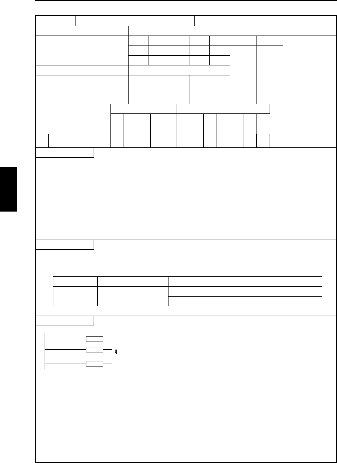
Chapter 5 Instruction Specifications
5-112
Item number Control instructions-11 Name Start interrupt scan program (INTERRUPT)
Ladder format Condition code Processing time (µs) Remark
R7F4 R7F3 R7F2 R7F1 R7F0 Average Maximum
INT n DER ERR SD V C
zzzzz
Instruction format Number of steps 0.5
Condition Steps
INT n 1
Bit Word Double word
Usable I/O XY
R,
M
TD, SS,
CU, CT WX WY
WR,
WM TC DX DY
DR,
DM
Constant
Other
n Interrupt priority {0 to 2 , 16 to 19, 20
to 27 (Decimal)
Function
•This instruction declares the start of an interrupt scan program.
•n = 0 to 2 indicates a periodical interrupt scan. n = 16 to 19 indicates interrupt input. n = 20 to 27 indicates an interrupt scan
when the counter input exceeds the preset value.
•It is set to the 10 ms periodic scan when n = 0, 20 ms periodic scan when n = 1, and 40 ms periodic interrupt scan when n =
2.
•The smaller the number n, the higher the interrupt priority.
•Always use INT n and RTI in pairs.
•Even if a startup condition is used for INT n, it will be ignored.
•Code the INT n to RTI subroutine program after the END instruction.
•The n in INT n cannot be used more than once within the same program.
Notes
•This instruction is checked prior to execution, and when there is an error, the following error code is set in the special
internal output WRF001. Also, the CPU error code '34' is set to special internal output WRF000.
CPU error code Special internal output Error code Error description
34 WRF001 H0005 Duplicate definition of INT
H0014 INT undefined
Instruction for use
END
INT 0
RTI
INT 0
scan
10 ms interrupt scan program
•The program between INT0 and RTI is started and executed every 10 ms.
INT n
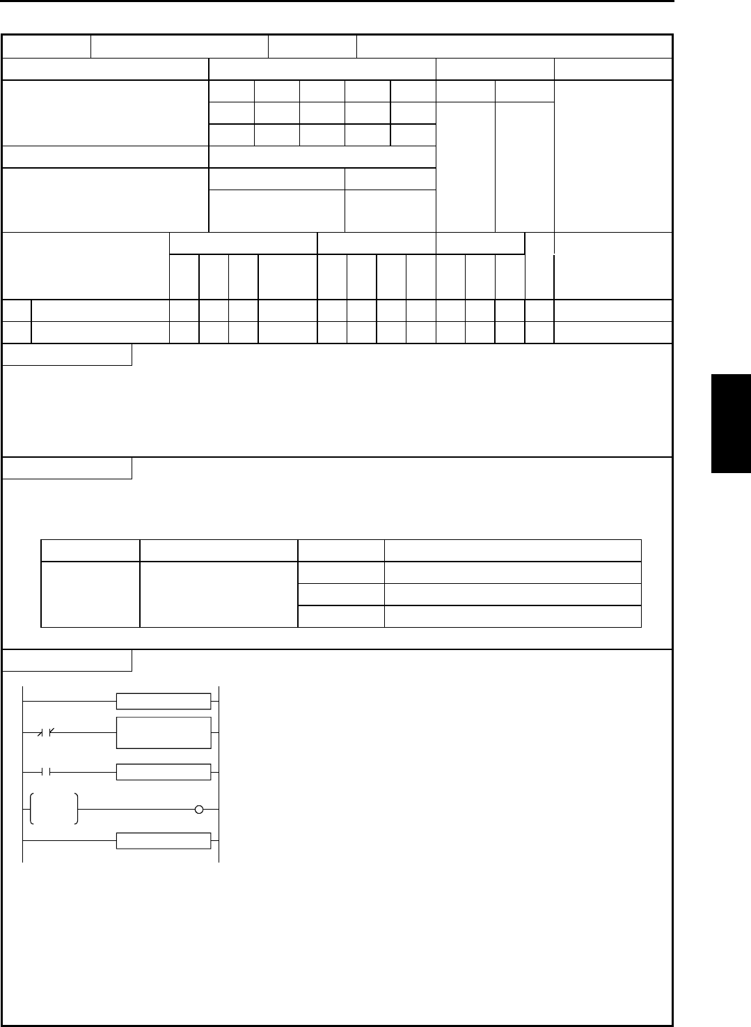
Chapter 5 Instruction Specifications
5-113
Item number Control instructions-12 Name End interrupt scan program (RETURN INTERRUPT)
Ladder format Condition code Processing time (µs) Remark
R7F4 R7F3 R7F2 R7F1 R7F0 Average Maximum
RTI DER ERR SD V C
zzzzz
Instruction format Number of steps 0.5
Condition Steps
RTI 1
Bit Word Double word
Usable I/O XY
R,
M
TD, SS,
CU, CT WX WY
WR,
WM TC DX DY
DR,
DM
Constant
Other
Function
•This instruction declares the end of an interrupt scan program.
•When this program is executed, the processing is returned to the program that was executing before the interrupt scan was
performed.
•Do not set a startup condition with this instruction.
Notes
•This instruction is checked prior to execution, and when there is an error, the following error code is set in the special
internal output WRF001. Also, the CPU error code '34' is set to special internal output WRF000.
CPU error code Special internal output Error code Error description
H0012 RTI undefined
34 WRF001 H0021 RTI area error
H0031 RTI startup condition error
Instruction for use
INT 0
WR0000=WR0000+1
WR0000=0
R000=0
RTI
X00000
X00000
WM000
< =
WR0000
SET
R000
•A 0.01s timer is created using 10 ms interval interrupt.
•WM000, WR0000 and R000 are used for the set value, progress value
and timer coil, respectively.
•When X00000 is off, the progress value and timer coil are cleared.
•When X00000 is on, the progress value increments by 1 every 10 ms.
•The timer coil is turned on upon WM000 is less than or equal to
WR0000.
RTI
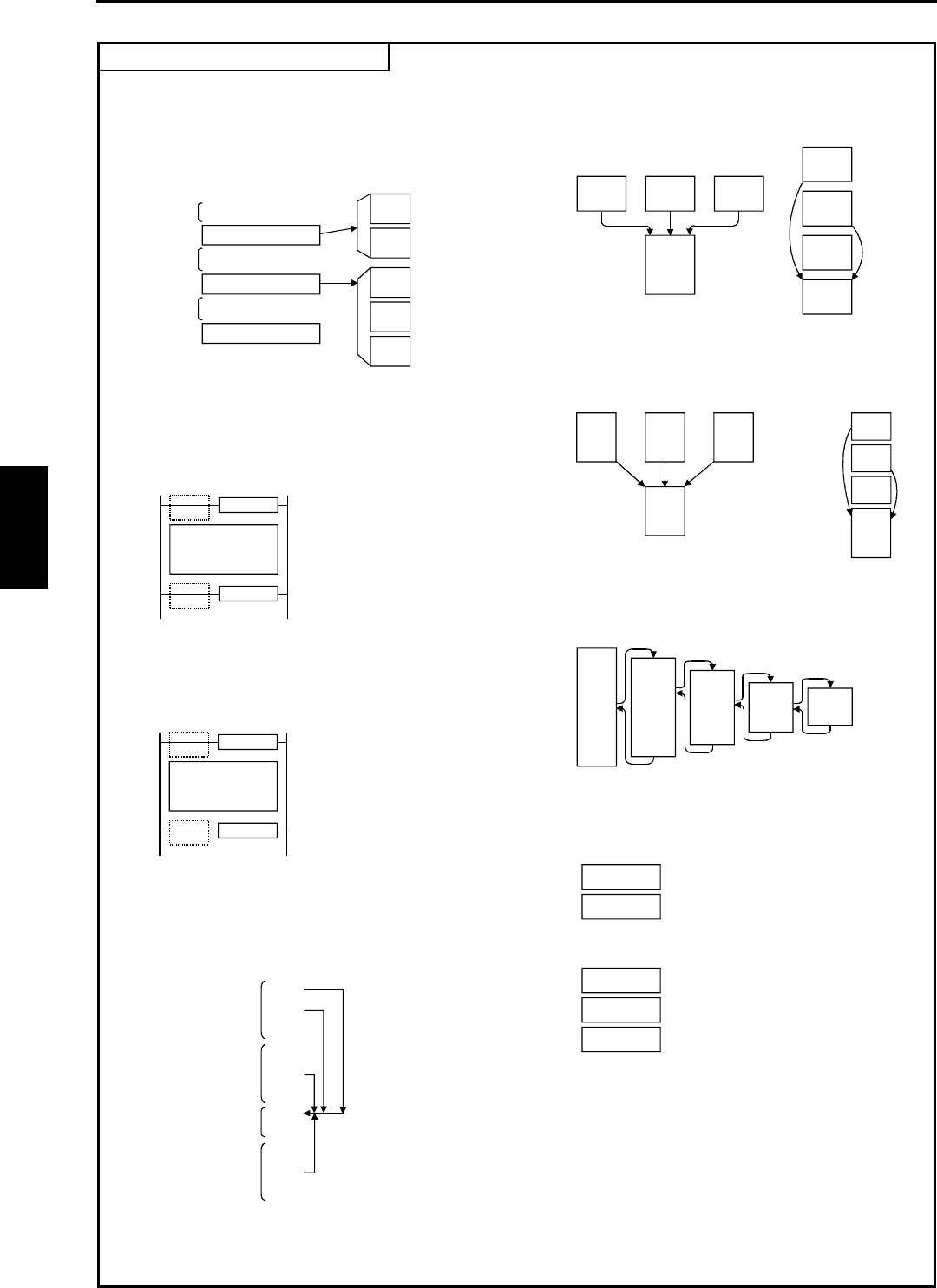
Chapter 5 Instruction Specifications
5-114
Syntax of SB n, RTS, INT n and RTI
SB 1
RTS
SB 2
RTS
RTS
RTS
RTS
SB 10
SB 11
SB 12
END
INT 1
RTI
INT 2
RTI
Program
SB n
RTS
Program
INT n
RT1
CAL 1
CAL 1
END
SB 2
CAL 1
RTS
SB 1
RTS
INI 0
CAL 1
RTI
SB 1
JMP 1
SB 2 SB 3
JMP 1
LBL 1
RTS
SB 1
JMP 1
SB 2
JMP 1
SB 3
LBL 1
RTS
INT 0
JMP 1
INT 1 INT 2
JMP 1
LBL 1
RTI
INT 0
JMP 1
INT 2
JMP 1
INT 1
RTI
SB 1
CAL 20
RTS
SB 20
CAL 30
RTS
SB 30
CAL 40
RTS RTS
CAL 50
SB 40 SB 50
RTS
1st level 2nd level 3rd level 4th level 5th level
END
SB 20
RTS
SB 1
RTS
SB 40
RTS
SB 30
RTS
SB 50
RTS
INT 0
RTI
LBL 1
1] A subroutine can be programmed between a normal scan
and interrupt scan, between two interrupt scans, or after
the final interrupt scan.
Normal scan
Interrupt
scan
Interrupt
scan
Program head
Subroutine area
Subroutine area
Subroutine area
Program end
Subroutine 1
Subroutine 2
Subroutine 10
Subroutine 11
Subroutine 12
5] It is also possible to program a subroutine with
multiple entry points and one exit.
2] Program the subroutine start (SB n) and subroutine
end (RTS) instructions without specifying startup
conditions.
Startup
condition
•The RTS startup condition error
will occur during operation pre-
processing.
6] It is also possible to program a interrupt scan with
many entry points and one exit.
7] Nesting of subroutines is allowed up to 5 levels.
Startup
condition
Startup
condition
Startup
condition
(1) As shown to the left, the subroutine
program order and nesting order
have no relationship.
4] The same subroutine can be called from a normal scan,
interrupt scan or subroutine.
Program head
Program head
3] Program the interrupt scan start (INT n) and scan complete
(RTI) instructions without specifying startup conditions.
Normal scan
Interrupt scan
Subroutine 2
Subroutine 1
RTI

Chapter 5 Instruction specifications
5-115
Item number Transfer command-1 Name General purpose port communication command
Ladder format Condition code Processing time (µs) Remark
R7F4 R7F3 R7F2 R7F1 R7F0 Average Maximum
TRNS 0 (d, s, t) DER ERR SD V C
↕zzzz
Command format Number of steps
Condition Steps
TRNS 0 (d, s, t) -5
80 2,078
Bit Word Double word
Usable I/O XY
R,
L,
M
TD, SS,
CU, CT WX WY
WR,
WM TC DX DY
DR,
DM Others
d Dummy {
s Parameter area {s to s+14
t Communication control {t to t+11
Function
(1) This is a command to send data via general purpose port. It is also possible to receive data after data sending.
(2) Parameter "d" is dummy. Assign WY10. (Actual data in Y100 to Y115 is not influenced.)
(3) Parameter "s" is starting address of parameter table for communication setting.
(4) Parameter "t" is starting address of bit table for communication control.
(5) "s" parameter
[0] Return code
s
s+1
s+4
s+6
s+7
s+9
s+A
s+B
s+C
s+D
s+E
[1] System area
(Do not use this area.)
[2] Timeout
[3] Address of sending area
[4] Reserve area for data sending (word)
[5] Address of receiving area
[6] Reserve area for data receiving (word)
[7] Receiving data length (byte)
[8] Start code
[9] End code
[10] Communication speed
[11] Communication format
: Access forbidden
: User settin
g
area
s+3
[0] Return code : Result of TRNS 0 command is set in
lower 8 bits.
Completed 0
Error ≠0
[1] System area : This area is used by system (CPU) while
TRNS 0 operation. It is not allowed for
users to use this area.
[2] Timeout : Timeout setting from command executed
to completed.
=0 : Timeout disabled
≠0 : Timeout enabled [×10ms]
Max. HFFFF
TRNS 0 (d, s, t)
! If this area is written, CPU might stop operation due to
system error.
Constant
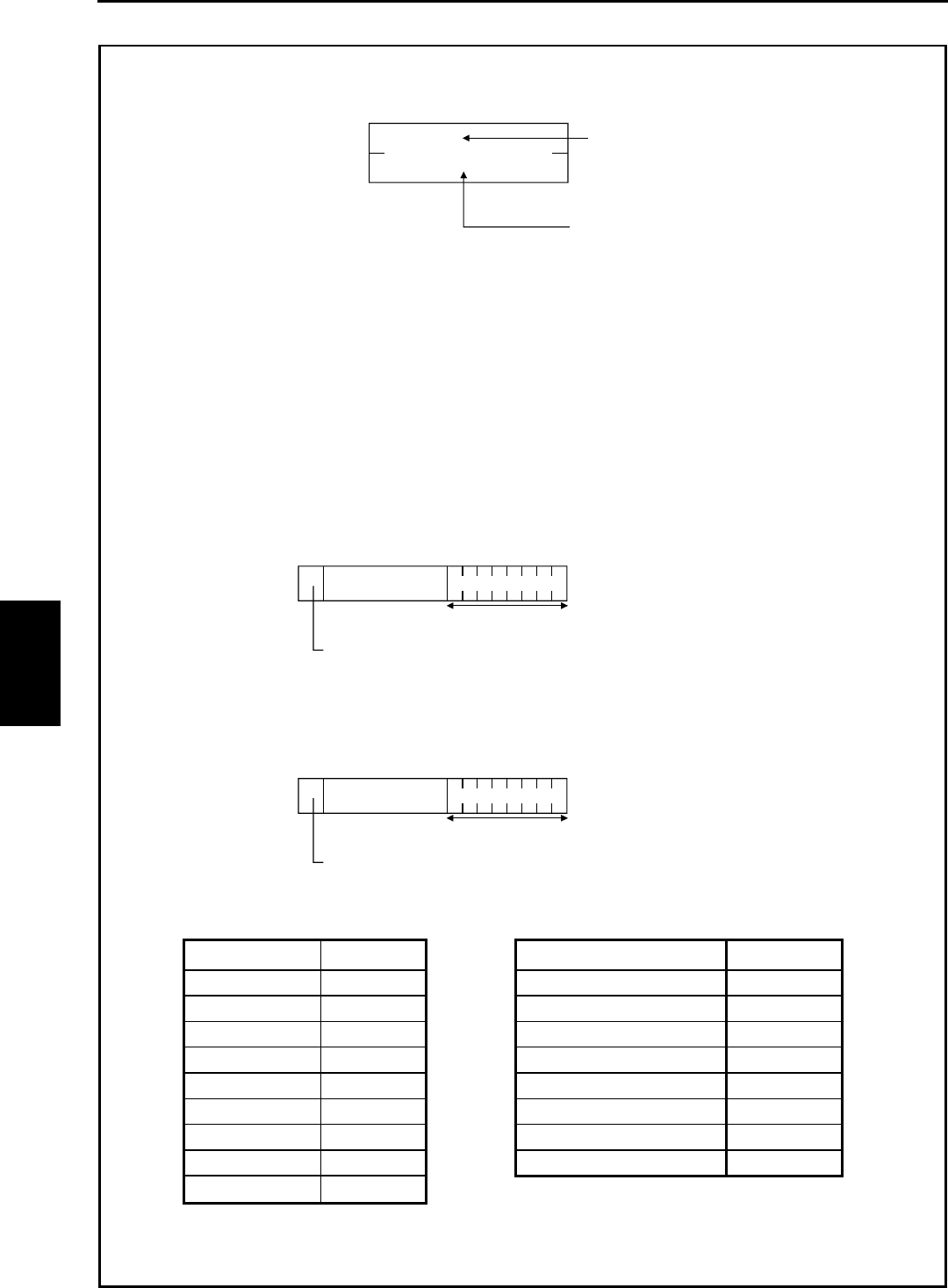
Chapter 5 Instruction specifications
5-116
[3] Address of sending area :
Address number and address type are configured in 2 words as below.
s+4
s+5
T
yp
e : WR → H000A
I/O No.: H0000 -
WM → H000C
[4] Reserved data size for data sending. : This is not actual data size but reserved size. Set it by "Word".
[5] Address of receiving area :
Address number and address type are configured in 2 words as below.
(Data format is as same as sending area.)
[6] Reserved data size for data receiving. : This is not actual data size but reserved size. Set it by "Word".
[7]*1 Receiving data length :
If receiving data is found by data length, set this parameter by "Byte". The maximum size is 1,024 byte. If data is
more than 1,024 bytes or reserved area, TRNS command fails with DER="1".
[8]*1 Start code :
If receiving data is found by start code, set this parameter.
b
15
b
7
b
0
Start code
(
H00 - HFF
)
= 0 : Start code disabled.
= 1 : Start code enabled.
[9]*1 End code :
If receiving data is found by end code, set this parameter.
b
15
b
7
b
0
End code
(
H00 - HFF
)
= 0 : End code disabled.
= 1 : End code enabled.
[10] Communication speed : [11] Communication format
Baud rate Value Format Value
300 bps H0000 7 bits, even parity, 2 stop H0000
600 bps H0001 7 bits, odd parity, 2 stop H0001
1,200 bps H0002 7 bits, even parity, 1 stop H0002
2,400 bps H0003 7 bits, odd parity, 1 stop H0003
4,800 bps H0004 8 bits, non parity, 2 stop H0004
9,600 bps H0005 8 bits, non parity, 1 stop H0005
19,200 bps H0006 8 bits, even parity, 1 stop H0006
38,400 bps H0007 8 bits, odd parity, 1 stop H0007
57,600 bps H0008
TRNS 0 (d, s, t)
Chapter 5 Instruction specifications
5-117
*1 Received data is defined by either of following 4 ways depending on setting in [7] s+A to [9] s+C.
(a) Start code and data size*2
s+A : Data length (Byte)
s+B : H80 (=Start code)
s+C : H0000
(b) Start and end code *2
s+A : H0000
s+B : H80 (=Start code)
s+C : H80 (=End code)
(c) End code
s+A : H0000
s+B : H0000
s+C : H80 (=End code)
(d) Data length
s+A : Data length (Byte)
s+B:H0000
s+C:H0000
*2 In case of start code used, CPU can fail to receive due to buffer size full if data with wrong start code is sent.
(6) "t" parameter
: Set by user[0][1][2][3][4][5][6][7][8][9][A][B]
tt+B
[0] Execution bit:
Set "1" by user program to send data. This bit is reset after communication completed.
[1] Communication completed :
This bit is set "1" when communication completed without error, and reset at communication starting.
[2] Communication failed :
This bit is set "1" when communication fails, and reset at communication starting.
[3] Initialize :
Set "1" by user program to initialize TRNS 0 command. If this bit is on while communication, the communication
is forced to be stopped.
[4] Initialize completed :
This bit is set "1" when initializing completed without error. Initialize bit [3] is reset at this timing.
[5] Receive enabled :
Set "1" by user program if CPU needs to receive data after data sending. This bit is reset after communication
completed.
[6] Parity error flag :
This bit is set "1" when parity error detected.
[7] Framing error :
This bit is set "1" when framing error detected.
[8] Overrun error :
This bit is set "1" when overrun error detected.
TRNS 0 (d, s, t)
Start code
Start code End code
End code
Data length
Data length
Chapter 5 Instruction specifications
5-118
[9] Timeout :
This bit is set "1" when timeout detected.
[A] Input buffer full :
This bit is set "1" when input buffer full
[B] Conflict error :
This bit is set "1" when TRNS 0 or RECV 0 commands are duplicated.
Bit [6] to [B] is reset at initializing and TRNS 0 executed.
(7) Sending/receiving data format
Set sending data as follows, and Receiving data is set as follows.
[1] Sending/receiving data byte is even. [2] Sending/receiving data byte is odd.
Sending/Receiving data byte (N)
1st b
y
te 2nd b
y
te
3rd b
y
te 4th b
y
te
5th b
y
te 6th b
y
te
7th b
y
te 8th b
y
te
N-1th b
y
te Nth b
y
te
…
Reserve area
for data
sending/receiving
Sending/Receiving byte (N)
1st b
y
te 2nd b
y
te
3rd b
y
te 4th b
y
te
5th b
y
te 6th b
y
te
7th b
y
te 8th b
y
te
Nth b
y
te
(
i
g
nored
)
…
N-2th b
y
te N-1th b
y
te
Caution
z Be sure to switch port type at first from dedicated port to general purpose port by FUN 5 command in user program.
z If CPU receives data by RECV command after data sending, received data could be failed depending on timing. In such a
case, TRNS command with "receive enabled" is recommended.
z No contact nor condition is allowed to use with TRNS 0 command.
z Be sure to set [0] Execution bit high in 2nd scan or later. (Not in 1st scan)
z If parameter setting is wrong, error code H52 (TRNS/RECV command error) is set in WRF000 in some cases.
z ER signal is set on in the following condition.
Communication executed properly.
z ER signal is set off in the following condition.
- Initialized bit being set "1" while communication.
- CPU status changed RUN→STOP→RUN while communication
- Timeout while communication.
- s, t parameters overwritten and range error while communication.
TRNS 0 (d, s, t)
Chapter 5 Instruction specifications
5-119
Sample program
Description
TRNS 0 parameter and sent data are configured at 1st scan by R7E3 contact.
When the switch is ON, execution bit R0 is ON, and data is sent out from CPU port.
TRNS 0 (d, s, t)
R7E3
WM103 = 0
WM104 = H000A
WM105 = H0000
WM106 = 16
WM107 = H000A
WM108 = H0100
WM109 = 256
WM10A = 0
WM10B = H8002
WM10C = H800D
WM10D = 6
WM10E = 0
WR10 = H0200
FUN 5 (WR10)
R7E3 : 1st scan ON
Timeout = 0
Reserve area for data sending :
16 words from WR0
Reserve area for data receiving :
256 words from WR100
Data receiving definition
Start code : H02, End code : H0D
Communication speed : 19.2k bps
Format : 7 bits, even, 2 stop
Port 2 confi
g
ured as
g
eneral
p
ur
p
ose
p
ort.
R7E3
WR100 = 9
WR101 = H0231
WR102 = H3830
WR103 = H3031
WR104 = H3338
WR105 = H0D00
Sent data : 9 bytes
Inverter (SJ300/L300P) command
FWD RUN for station No.18
02 31 38 30 30 31 33 38 0D
(STX 18 00 1 38 CR) [38=BCC]
Switch R0
TRNS 0 (WY10, WM100, R0)
When the switch is ON, execution bit R0 is ON, and
data is sent out from CPU port.
R5 enables data receiving from the other device.
WR0
WR100
DIF0
S
R5
S
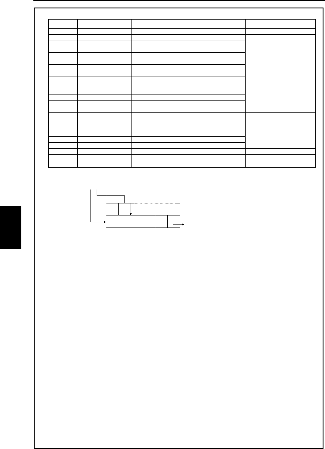
Chapter 5 Instruction specifications
5-120
TRNS/RECV command return code table
Return code Name Description Countermeasure
H00 Completed properly Operation completed without error -
H21 Range error Parameter "s" and "t" is out of available I/O range.
H22 Reserve area for sending
setting error Parameter setting is wrong.
H23 Reserve area for sending
range error Parameter is out of available I/O range.
H24 Reserve area for receiving
setting error Parameter setting is wrong.
H25 Reserve area for receiving
range error Parameter is out of available I/O range.
H26 Sending data error Configured sending data length is beyond reserve area
H27 Receiving data error Configured receiving data length is beyond reserve area
H28 Area overlapping error
*2 Parameter s, t, or reserve area is overlapped.
Set right value.
H30 Timeout *1 Communication is not completed within configured time. Set longer timeout or check the
program.
H40 Receiving area over *3 Received data is beyond reserved area Configure bigger size
H41 Parity error *4 Parity error detected
H42 Framing error *4 Framing error detected
H43 Overrun error detected Overrun error detected
Check wiring and data format.
H44 Conflict error TRNS 0/RECV 0 duplicated Execute one by one
H45 Parameter error Baud rate or format setting is wrong Set right value.
H46 Port type error Port type is not general purpose port. Configure general purpose port.
*2 Area overlapping error (H28) is not detected in the following case.
TRNS n
(
d
,
s
,
t
)
b
15
b
0
t+1 t
t+2 Data overlapping
If starting area of "s" parameter and "t" parameter is overlapped, error code H21 can be set instead of H28.
*3 Received data is stored as long as reserved area. (1,024 bytes)
*4 Data is not guaranteed.
TRNS 0 (d, s, t)
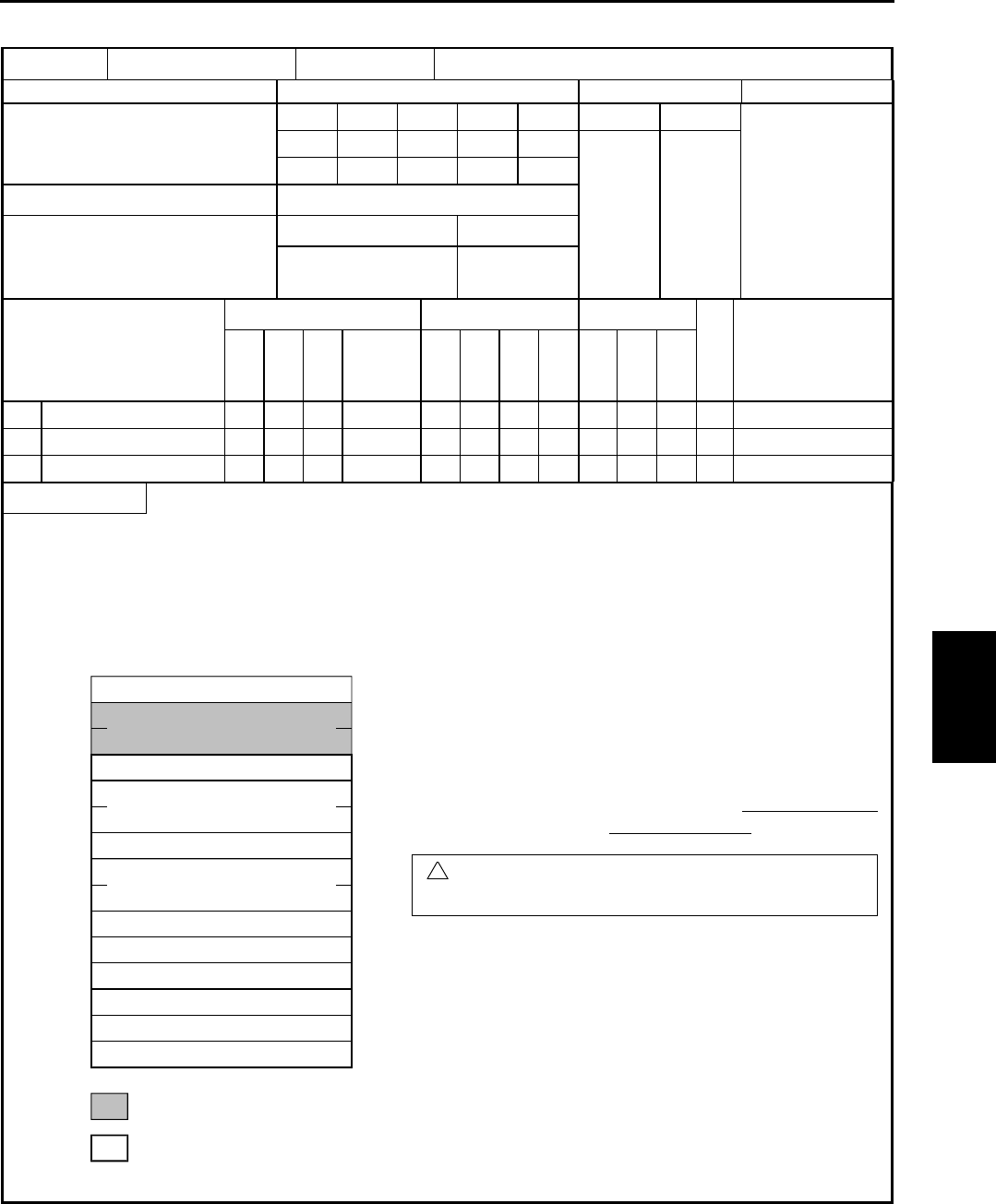
Chapter 5 Instruction specifications
5-121
Item number Transfer command-2 Name General purpose port communication command
Ladder format Condition code Processing time (µs) Remark
R7F4 R7F3 R7F2 R7F1 R7F0 Average Maximum
RECV 0 (d, s, t) DER ERR SD V C
↕zzzz
Command format Number of steps
Condition Steps
RECV 0 (d, s, t) -5
80 2,064
Bit Word Double word
Usable I/O XY
R,
L,
M
TD, SS,
CU, CT WX WY
WR,
WM TC DX DY
DR,
DM Others
d Dummy {
s Parameter area {s to s+14
t Communication control {t to t+11
Function
(1) This is a command to send data via general purpose port. It is also possible to receive data after data sending.
(2) Parameter "d" is dummy. Assign WX0. (Actual data in X00 to X15 is not influenced.)
(3) Parameter "s" is starting address of parameter table for communication setting.
(4) Parameter "t" is starting address of bit table for communication control.
(5) "s" parameter
[0] Return code
s
s+1
s+4
s+6
s+7
s+9
s+A
s+B
s+C
s+D
s+E
[1] System area
(Do not use this area.)
[2] Timeout
[3] Address of sending area
[4] Reserve area for data sending (word)
[5] Address of receiving area
[6] Reserve area for data receiving (word)
[7] Receiving data length (byte)
[8] Start code
[9] End code
[10] Communication speed
[11] Communication format
: Access forbidden
: User settin
g
area
s+3
[0] Return code : Result of RECV 0 command is set in
lower 8 bits.
Completed 0
Error ≠0
[1] System area : This area is used by system (CPU) while
RECV 0 operation. It is not allowed for
users to use this area.
[2] Timeout : Timeout setting from command executed
to completed.
=0 : Timeout disabled
≠0 : Timeout enabled [×10ms]
Max. HFFFF
RECV 0 (d, s, t)
! If this area is written, CPU might stop operation due to
system error.
Constant

Chapter 5 Instruction specifications
5-122
[3] Address of sending area :
Address number and address type are configured in 2 words as below.
s+4
s+5
T
yp
e : WR → H000A
I/O No.: H0000 -
WM → H000C
[4] Reserved data size for data sending. : This is not actual data size but reserved size. Set it by "Word".
[5] Address of receiving area :
Address number and address type are configured in 2 words as below.
(Data format is as same as sending area.)
[6] Reserved data size for data receiving. : This is not actual data size but reserved size. Set it by "Word".
[7]*1 Receiving data length :
If receiving data is found by data length, set this parameter by "Byte". The maximum size is 1,024 byte. If data is
more than 1,024 bytes or reserved area, RECV command fails with DER="1".
[8]*1 Start code :
If receiving data is found by start code, set this parameter. (See TRNS command)
[9]*1 End code :
If receiving data is found by end code, set this parameter. (See TRNS command)
[10] Communication speed (See TRNS command)
[11] Communication format (See TRNS command)
*1 Received data is defined by either of following 4 ways depending on setting in [7] s+A to [9] s+C.
*2 In case of start code used, CPU can fail to receive due to buffer size full if data with wrong start code is sent.
RECV 0 (d, s, t)

Chapter 5 Instruction specifications
5-123
(6) "t" parameter
: Set by user[0][1][2][3][4][5][6][7][8][9][A][B]
tt+B
[0] Execution bit:
Set "1" by user program to send data. This bit is reset after communication completed.
[1] Communication completed :
This bit is set "1" when communication completed without error, and reset at communication starting.
[2] Communication failed :
This bit is set "1" when communication fails, and reset at communication starting.
[3] Initialize :
Set "1" by user program to initialize RECV 0 command. If this bit is on while communication, the communication
is forced to be stopped.
[4] Initialize completed :
This bit is set "1" when initializing completed without error. Initialize bit [3] is reset at this timing.
[5] Send enabled :
Set "1" by user program if CPU needs to send data after data receiving. This bit is reset after communication
completed.
[6] Parity error flag :
This bit is set "1" when parity error detected.
[7] Framing error :
This bit is set "1" when framing error detected.
[8] Overrun error :
This bit is set "1" when overrun error detected.
[9] Timeout :
This bit is set "1" when timeout detected.
[A] Input buffer full :
This bit is set "1" when input buffer full
[B] Conflict error :
This bit is set "1" when TRNS 0 or RECV 0 commands are duplicated.
Bit [6] to [B] is reset at initializing and RECV 0 executed.
(7) Sending/receiving data format (See TRNS 0 command)
Caution
z Be sure to switch port type at first from dedicated port to general purpose port by FUN 5 command in user program.
z If CPU receives data by RECV command after data sending, sent data could be failed depending on timing. In such a case,
RECV command with "send enabled" is recommended.
z No contact nor condition is allowed to use with RECV 0 command.
z Be sure to set [0] Execution bit high in 2nd scan or later. (Not in 1st scan)
z If parameter setting is wrong, error code H52 (TRNS/RECV command error) is set in WRF000 in some cases.
z ER signal is set on in the following condition.
Communication executed properly.
z ER signal is set off in the following condition.
- Initialized bit being set "1" while communication.
- CPU status changed RUN→STOP→RUN while communication
- Timeout while communication.
- s, t parameters overwritten and range error while communication.
RECV 0 (d, s, t)
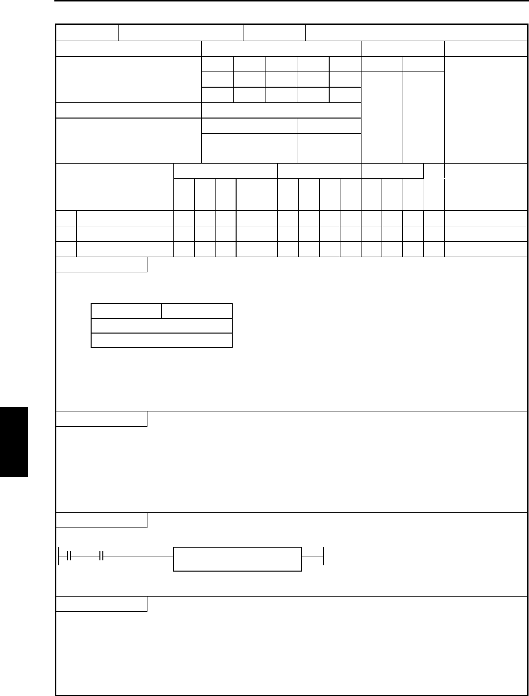
Chapter 5 Instruction Specifications
5-124
Item number FUN instructions-1 Name General purpose port switching
Ladder format Condition code Processing time (µs) Remark
R7F4 R7F3 R7F2 R7F1 R7F0 Average Maximum
FUN 5 (s) DER ERR SD V C
↕zzzz
Instruction format Number of steps 114 -
Condition Steps
FUN 5 (s) — 3
Bit Word Double word
Usable I/O XY
R,
M
TD, SS,
CU, CT WX WY
WR,
WM TC DX DY
DR,
DM
Constant
Other
sArgument {
s+1 (system area) {
s+2 (system area) {
Function
This command is to switch dedicated port (programming port) to general purpose port.
S Port number Current setting
System area
System area
S+1
S+2
Port number
H01 : Port 1
H02 : Port 2
* Error with the other values
Current setting
H00 : Dedicated port (Programming port)
H01 : Port 1 is general purpose port
H02 : Port 2 is general purpose port
Notes
•General purpose port can be configured only one port. If either port is configured general purpose port, FUN 5 command for
the other port is ignored with DER=1.
•General purpose works only when CPU is in RUN mode. When CPU status is in STOP, the port is automatically switched
back to dedicated port (programming port).
•It is impossible to switch from general purpose to dedicated port while CPU is in RUN status.
•FUN 5 does not work if port 1 is configured as modem mode.
Program example
X00000 DIF0 LD X00000
AND DIF0
[
WR0100 = H0200
]
WR0100 = H0200
FUN 5 (WR0100)
FUN 5
(
WR0100
)
Program description
Port 2 is switched to general purpose port at rising edge of X0000 input.
FUN 5 (s)
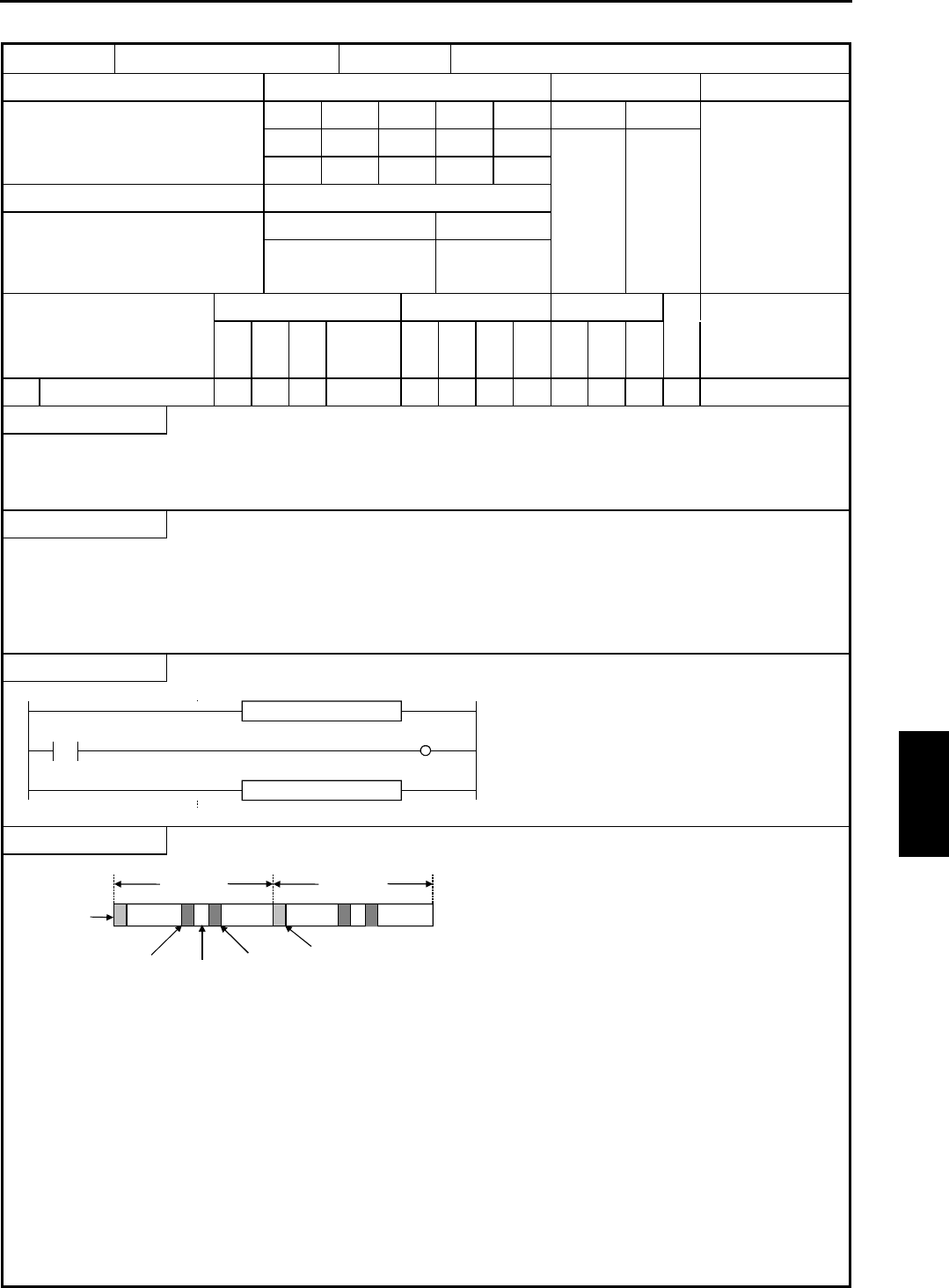
Chapter 5 Instruction Specifications
5-125
Item number FUN instructions-2 Name I/O refresh (All points)
Ladder format Condition code Processing time (µs) Remark
R7F4 R7F3 R7F2 R7F1 R7F0 Average Maximum
FUN 80 (s) DER ERR SD V C
* (ALREF (s)) ↕zzzz
Instruction format Number of steps 432
Condition Steps
FUN 80 (s) — 3
* (ALREF (s))
Bit Word Double word
Usable I/O XY
R,
M
TD, SS,
CU, CT WX WY
WR,
WM TC DX DY
DR,
DM
Constant
Other
s Argument (dummy) {
Function
•This instruction performs I/O refresh of all data in the external I/Os (including link area) during scanning.
* ( ) indicates the display when the Ladder Editor is used.
Notes
•This instruction performs I/O refresh of all external I/Os.
If refresh of certain area is to be performed, use FUN81 or FUN82.
•If the argument s exceeds the maximum I/O number, DER is set to “1” and no processing will be performed.
•Assign argument s as a one-word dummy. The I/O specified for argument s (WR and WM) will not be affected.
Program example
FUN 80 (WR0)
FUN 80 (WR0)
X0 Y100
1]
2]
3]
Program description
I/O refresh
1 scan 1 scan
FUN 80 1]
Program execution 2]
FUN 80 3] I/O refresh
FUN 80 (s)

Chapter 5 Instruction Specifications
5-126
Item number FUN instructions-3 Name I/O refresh (Input/output)
Ladder format Condition code Processing time (µs) Remark
R7F4 R7F3 R7F2 R7F1 R7F0 Average Maximum
FUN 81 (s) DER ERR SD V C
* (IOREF (s)) ↕zzzz
Instruction format Number of steps 244
Condition Steps
FUN 81 (s) — 3
* (IOREF (s))
Bit Word Double word
Usable I/O XY
R,
M
TD, SS,
CU, CT WX WY
WR,
WM TC DX DY
DR,
DM
Constant
Other
sType {
Function
s Input type H00: Input refresh
H01: Output refresh
•Depending on the I/O type of the area specified by s, refresh is performed with respect to I/O modules only, output modules
only.
•Refresh is performed by each slot assignment according to the I/O assignment.
•If the refresh processing is completed normally, DER is set to '0.'
* ( ) indicates the display when the Ladder Editor is used.
Notes
•If the I/O type is other than H00 or H01, DER is set to “1” and no processing will be performed.
•If the argument s exceeds the maximum I/O number, DER is set to “1” and no processing will be performed.
Program example
R000 LD R000
AND DIF0
[
WR0004 = 0
FUN 81 (WR0004)
]
LD R001
AND DIF1
[
WR0004 = 1
FUN 81 (WR0004)
]
R001 DIF1
WR0004 = 0
FUN 81 (WR0004 )
DIF0
WR0004 = 1
FUN 81 (WR0004 )
Program description
•Upon leading of R000, the input module is refreshed.
•Upon leading of R001, the output module is refreshed.
FUN 81 (s)
Chapter 5 Instruction Specifications
5-127
Item number FUN instructions-4 Name I/O Refresh (slot)
Ladder format Condition code Processing time (µs) Remark
R7F4 R7F3 R7F2 R7F1 R7F0 Average Maximum
FUN 82 (s) DER ERR SD V C
* (SLREF (s)) ↕zzzz
Instruction format Number of steps 311
Condition Steps
FUN 82 (s) — 3
* (SLREF (s))
Bit Word Double word
Usable I/O XY
R,
M
TD, SS,
CU, CT WX WY
WR,
WM TC DX DY
DR,
DM
Constant
Other
s Number of points {
s+1 and
beyond Slot location number {Designate the slot
location.
Function
s
s+1
s+2
:
:
s+n
Number of points to be refreshed
Refresh slot location number
Refresh slot location number
Refresh slot location number
n ≤ 64
Refresh slot location number is
designated by unit and slot number.
:
:
•Performs refresh of the designated module for the number of points specified by s, starting with area s+1.
•Refresh is performed by slot.
•The slot location numbers stored in areas s+1 and subsequent are designated by the unit number and slot number.
•The maximum number of points to be refreshed (n) is 64 points. The points exceeding 64 points are not refreshed.
•If refresh processing is completed normally, DER is set to “0.”
* ( ) indicates the display when the Ladder Editor is used.
Program example
R000 DIF0
WR0000 = H0002
WR0001 = H0000
WR0002 = H0010
FUN 82
(
WR0000
)
LD R000
AND DIF0
[
WR0000 = H0002
WR0001 = H0000
WR0002 = H0010
FUN82 (WR0000)
]
Program description
•Upon leading of R000, the two slots designated after WR0001 (unit 0, slot 0) and (unit 1, slot 0) are refreshed.
FUN 82 (s)

Chapter 5 Instruction Specifications
5-128
Notes
•Set the unit number (0 to 3) and slot number (0 to 1) after s+1. For other set values, DER is set to “1” and that slot will not
be processed.
•If there is no I/O assignment to the designated slot, DER is set to “1” and that slot will not be processed.
•If the number of s+n points exceeds the maximum I/O number, DER is set to “1” and no processing will be performed.
•If the number of points exceeds 64, DER is set to “1” and the points exceeding 64 will not be processed (refresh will be
performed for up to 64 points).
Slot location number
The slot locations are designated using the unit number and slot number.
The unit number and slot number are set as follows in one word units:
0 to 0
b12b15 b7 b3 b0
0 to 0 Unit number Slot number
FUN 82 (s)
Chapter 5 Instruction Specifications
5-129
Item number FUN instructions-5 Name High-speed Counter Operation Control
Ladder format Condition code Processing time (µs) Remark
R7F4 R7F3 R7F2 R7F1 R7F0 Average Maximum
FUN 140 (s) DER ERR SD V C
↕zzzz
Instruction format Number of steps 147
Condition Steps
FUN 140 (s) — 3
Bit Word Double word
Usable I/O XY
R,
M
TD, SS,
CU, CT WX WY
WR,
WM TC DX DY
DR,
DM
Constant
Other
s
Argument (Counter
number, operation
control value)
{
Function
Counter number: H01 to H04
Operation instruction: H00 – Stop,
H01 – Start
•Performs the starting and stopping of the count operation for the specified counter.
Notes
•If a value other than H01 to H04 is specified for the counter number and the operation instruction is set to a value other than
H00 or H01, DER will be set to “1” and no processing will be performed.
•If the specified counter number is set to a function other than a corresponding external I/O counter (single-phase counter,
two-phase counter), DER will be set to “1” and no processing will be performed.
•Since Counter 4 is invalid when a 10-point CPU is used, if Counter 4 is specified, DER will be set to “1” and no processing
will be performed.
•If the specified counter number is unable to make an output (PI/O function setting result by R7F5), DER will be set to “1”
and no processing will be performed.
•This instruction is only used to start and stop the counter operation. Other counter settings will not be changed.
•The counter operation will start after the power is turned back on even if the power is turned off when the count operation is
stopped by this instruction. The operation of the high-speed counter will be stopped only when this instruction specifies the
stop instruction.
•The counter operation will continue when the CPU operation is stopped.
•When the count operation stops, the progress value update also stops. When starting the count operation, the progress value
is cleared and then the operation starts.
Program example
R0
LD R0
AND DIF0
[
WR0 = H101
FUN 140 ( WR0 )
]
DIF0 WR0 = H0101
FUN 140 (WR0)
Program description
•Prior to starting a counter operation, various settings required for the counter operation are reflected in the special internal
outputs, and the PI/O function setting flag (R7F5) is turned on while the CPU is being stopped.
For details on the special internal output settings, see Chapter 8.
Starts the counter No. 1 operation.
SCounter number Operation instruction
15 8 7 0
FUN 140 (s)
Chapter 5 Instruction Specifications
5-130
Item number FUN instructions-6 Name High-speed Counter Coincidence Output Control
Ladder format Condition code Processing time (µs) Remark
R7F4 R7F3 R7F2 R7F1 R7F0 Average Maximum
FUN 141 (s) DER ERR SD V C
↕zzzz
Instruction format Number of steps 138
Condition Steps
FUN 141 (s) — 3
Bit Word Double word
Usable I/O XY
R,
M
TD, SS,
CU, CT WX WY
WR,
WM TC DX DY
DR,
DM
Constant
Other
s
Argument (Counter
number, output
instruction)
{
Function
Counter number: H01 to H04
Output instruction: H00 – Coincidence output disable,
H01 – Coincidence output able
•Performs the enabling and disabling of the coincidence output for the specified counter.
•Output is turned off when the coincidence output disabling instruction is issued while coincidence output is being performed
(while coincidence output is on).
Notes
•If a value other than H01 to H04 is specified for the counter number and the output instruction is set to a value other than
H00 or H01, DER will be set to “1” and no processing will be performed.
•If the specified counter number is set to a function other than a corresponding external I/O counter (single-phase counter,
two-phase counter), DER will be set to “1” and no processing will be performed.
•Since Counter 4 is invalid when a 10-point CPU is used, if Counter 4 is specified, DER will be set to “1” and no processing
will be performed.
•If the specified counter number is unable to make an output (PI/O function setting result by R7F5), DER will be set to “1”
and no processing will be performed.
•This instruction is only used to enable and disable the coincidence output. Other counter settings will not be changed and it
will not affect the count operation.
•When coincidence output is enabled by this instruction when the coincidence conditions are already established, coincidence
output will be turned on when the instruction is issued.
•The control contents of this instruction will be reflected in the output control flag (R7FC to R7FF) of the corresponding
counter number.
•When the CPU is not operating, the counter coincidence output continues/stops according to the setting of the special
internal output (output selection at R7DC stop).
Program example
R1 LD R1
AND DIF1
[
WR1 = H101
FUN 141 ( WR1 )
]
DIF1 WR1 = H0101
FUN 141 (WR1)
Program description
•Sets the coincidence output validity for the counter No. 1.
Because the counter coincidence output Yxxx cannot be used in the ladder program (including the monitor, etc.), do not use
it for the coil such as a contact.
SCounter number Operation instruction
15 8 7 0
FUN 141 (s)

Chapter 5 Instruction Specifications
5-131
Item number FUN instructions-7 Name High-speed Counter Up-Count/Down-count Control (Single
phase counter only)
Ladder format Condition code Processing time (µs) Remark
R7F4 R7F3 R7F2 R7F1 R7F0 Average Maximum
FUN 142 (s) DER ERR SD V C
↕zzzz
Instruction format Number of steps 156
Condition Steps
FUN 142 (s) — 3
Bit Word Double word
Usable I/O XY
R,
M
TD, SS,
CU, CT WX WY
WR,
WM TC DX DY
DR,
DM
Constant
Other
s
Argument (Counter
number, Up/Down
instruction)
{
Function
Counter number: H01 to H04
Up/down instruction: H00 – Up-count,
H01 – Down-count
•This controls the up-count/down-count of the specified counter.
•Up-count and down-count control can be performed during the count operation.
Notes
•If a value other than H01 to H04 is specified for the counter number and the up/down instruction is set to a value other than
H00 or H01, DER will be set to “1”and no processing will be performed.
•If the specified counter number is set to a function other than single-phase counter, DER will be set to “1” and no processing
will be performed.
•Since Counter 4 is invalid when a 10-point CPU is used, if Counter 4 is specified, DER will be set to “1” and no processing
will be performed.
•If the specified counter number is unable to make an output (PI/O function setting result by R7F5), DER will be set to “1”
and no processing will be performed.
•This instruction is only used to control the up-count and down-count. Other counter settings will not be changed and it will
not affect the count operation.
•The control contents of this instruction will be reflected in bits 11 to 8 of the special internal output WRF07E of the
corresponding counter number.
Program example
R2 LD R2
AND DIF2
[
WR2 = H101
FUN 142 ( WR2 )
]
DIF2 WR2 = H0101
FUN 142 (WR2)
Program description
•Switches the counter operation of the counter No. 1 to down count.
The count edges (leading/trailing) will follow the specification of the special internal output (WRF07E).
SCounter number Up/Down instruction
15 8 7 0
FUN 142 (s)
Chapter 5 Instruction Specifications
5-132
Item number FUN instructions-8 Name High-speed Counter Current Value Replacement
Ladder format Condition code Processing time (µs) Remark
R7F4 R7F3 R7F2 R7F1 R7F0 Average Maximum
FUN 143 (s) DER ERR SD V C
↕zzzz
Instruction format Number of steps 175
Condition Steps
FUN 143 (s) — 3
Bit Word Double word
Usable I/O XY
R,
M
TD, SS,
CU, CT WX WY
WR,
WM TC DX DY
DR,
DM
Constant
Other
sArgument (counter
number) {
s+1
Argument
(Replacement value
storage area)
{
Function
Counter number: H01 to H04
**: Disable area
•The counter value of the specified counter number will be replaced by the data stored in the replacement value storage area.
Notes
•If a value other than H01 to H04 is specified for the counter number, DER will be set to “1” and no processing will be
performed.
•If the specified counter number is set to a function other than a corresponding external I/O counter (single-phase counter,
two-phase counter), DER will be set to “1”and no processing will be performed.
•Since Counter 4 is invalid when a 10-point CPU is used, if Counter 4 is specified, DER will be set to “1” and no processing
will be performed.
•If the specified counter number is unable to make an output (PI/O function setting result by R7F5), DER will be set to “1”
and no processing will be performed.
•This instruction is only used to rewrite the count value. Other counter settings will not be changed and will not affect the
count operation.
•If the range for S exceeds the valid range of the I/O, DER will be set to “1” and no processing will be performed.
Program example
R3 LD R3
AND DIF3
[
WR30 = H100
WR31 = 1000
FUN 143 (WR30)
]
DIF3 WR30 = H0100
WR31 = 1000
FUN 143 (WR30)
Program description
•Rewrite the count value of the counter No. 1 to 1000.
SCounter number * *
15 8 7 0
S + 1 Replacement value storage area
FUN 143 (s)

Chapter 5 Instruction Specifications
5-133
Item number FUN instructions-9 Name High-speed counter current value reading
Ladder format Condition code Processing time (µs) Remark
R7F4 R7F3 R7F2 R7F1 R7F0 Average Maximum
FUN 144 (s) DER ERR SD V C
↕zzzz
Instruction format Number of steps 132
Condition Steps
FUN 144 (s) — 3
Bit Word Double word
Usable I/O XY
R,
M
TD, SS,
CU, CT WX WY
WR,
WM TC DX DY
DR,
DM
Constant
Other
sArgument (counter
number) {
s+1
Argument
(Current value storage
area)
{
Function
Counter number: H01 to H04
**: Disable area
•This function reads the count value of the specified counter number and writes it to the current value storage area.
Notes
•If a value other than H01 to H04 is specified for the counter number, DER will be set to “1” and no processing will be
performed.
•If the specified counter number is set to a function other than a corresponding external I/O counter (single-phase counter,
two-phase counter), DER will be set to “1”and no processing will be performed.
•Since Counter 4 is invalid when a 10-point CPU is used, if Counter 4 is specified, DER will be set to “1” and no processing
will be performed.
•If the specified counter number is unable to make an output (PI/O function setting result by R7F5), DER will be set to “1”
and no processing will be performed.
•This instruction is only used to read the count value. Other counter settings will not be changed and it will not affect the
count operation.
•The execution of this instruction will not change WRF07A to WRF07D (strobe area) and WRF056 (strobe complete flag).
•If the range for S exceeds the valid range of the I/O, DER will be set to “1” and no processing will be performed.
Program example
R4 LD R4
AND DIF4
[
WR40 = H100
FUN 144 ( WR40 )
]
LD (WR41 < 2000)
OUT R144
DIF4 WR40 = H0100
FUN 144 (WR40)
WR41
<
2000
R144
Program description
•Load the count value of the counter No. 1 to WR41.
If the count value of the counter No. 1 is less than 2000, R144 is turned on.
SCounter number * *
15 8 7 0
S + 1 Current value storage area
FUN 144 (s)
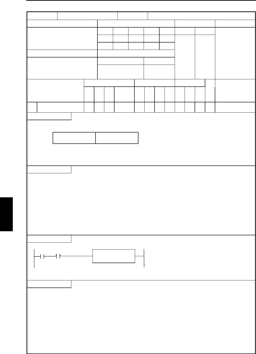
Chapter 5 Instruction Specifications
5-134
Item number FUN instructions-10 Name High-speed counter current value clear
Ladder format Condition code Processing time (µs) Remark
R7F4 R7F3 R7F2 R7F1 R7F0 Average Maximum
FUN 145 (s) DER ERR SD V C
↕zzzz
Instruction format Number of steps 157
Condition Steps
FUN 145 (s) — 3
Bit Word Double word
Usable I/O XY
R,
M
TD, SS,
CU, CT WX WY
WR,
WM TC DX DY
DR,
DM
Constant
Other
sArgument (counter
number) {
Function
Counter number: H01 to H04
**: Disable area
•The output value will be changed according to the output condition (on-preset value, off-preset value settings) if the count
value of the specified counter number is cleared and coincidence output is possible.
Notes
•If a value other than H01 to H04 is specified for the counter number, DER will be set to “1” and no processing will be
performed.
•If the specified counter number is set to a function other than a corresponding external I/O counter (single-phase counter,
two-phase counter), DER will be set to “1” and no processing will be performed.
•Since Counter 4 is invalid when a 10-point CPU is used, if Counter 4 is specified, DER will be set to “1” and no processing
will be performed.
•If the specified counter number is unable to make an output (PI/O function setting result by R7F5), DER will be set to “1”
and no processing will be performed.
•This instruction is used only to clear the count value. Other counter settings will not be changed and it will not affect the
count operation.
Program example
R5 LD R5
AND DIF5
[
WR5 = H100
FUN 145 ( WR5 )
]
DIF5 WR5 = H0100
FUN 145 (WR5)
Program description
•The count value of the counter No. 1 is cleared.
SCounter number * *
15 8 7 0
FUN 145 (s)
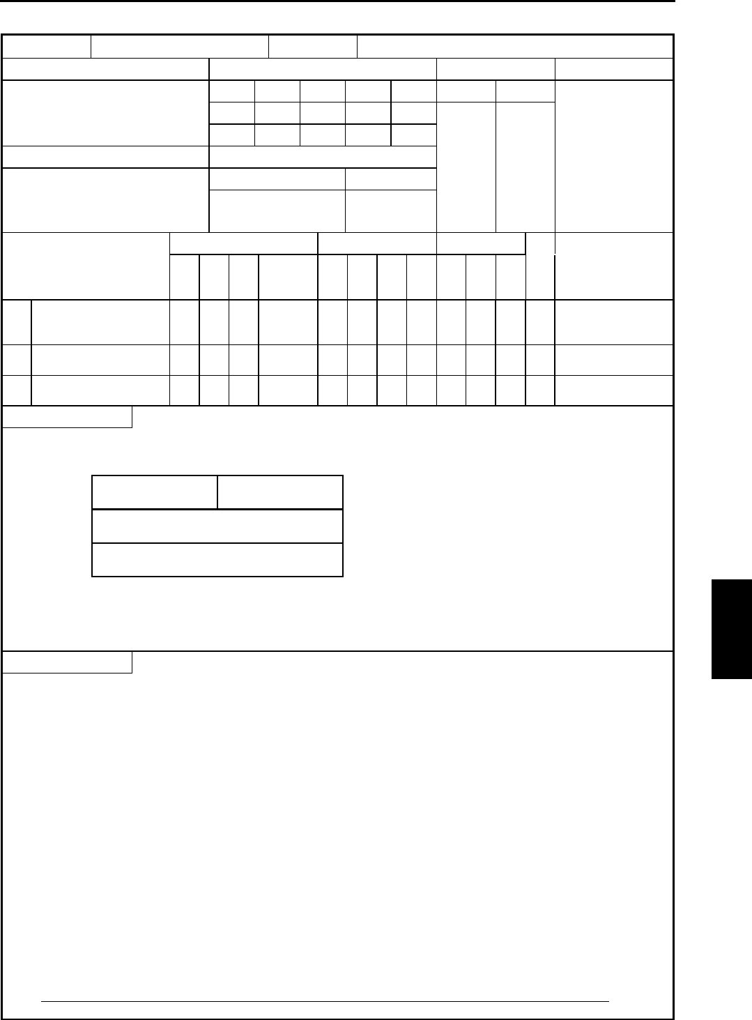
Chapter 5 Instruction Specifications
5-135
Item number FUN instructions-11 Name High-speed counter preset
Ladder format Condition code Processing time (µs) Remark
R7F4 R7F3 R7F2 R7F1 R7F0 Average Maximum
FUN 146 (s) DER ERR SD V C
↕zzzz
Instruction format Number of steps 162
Condition Steps
FUN 146 (s) — 3
Bit Word Double word
Usable I/O XY
R,
M
TD, SS,
CU, CT WX WY
WR,
WM TC DX DY
DR,
DM
Constant
Other
s
Argument (counter
number, preset
specification)
{
s+1 Argument
(on-preset value) {
s+2 Argument
(off-preset value) {
Function
Counter number: H01 to H04
Preset specification: H00 – Specification of on-preset
value and off-preset value
H01 – Specification of on-preset
value only
H02 – Specification of off-preset
value only
•The on-preset value and off-preset value will be set according to the preset specifications for the specified counter number.
•The coincidence output value will remain unchanged even when coincidence output is possible.
Notes
•If a value other than H01 to H04 is specified for the counter number and a value other than H00 to H02 is set for the preset
specification, DER will be set to “1” and no processing will be performed.
•Since Counter 4 is invalid when a 10-point CPU is used, if Counter 4 is specified, DER will be set to “1” and no processing
will be performed.
•If the specified counter number is set to a function other than a corresponding external I/O counter (single-phase counter,
two-phase counter), DER will be set to “1” and no processing will be performed.
•The specified preset value will be checked using the criteria shown below. If an error occurs, DER will be set to “1” and no
processing will be performed.
If there is no error, the bit respective to the setting error detail information WRF057 will be set to “0” and releases the
operation disabled status.
1] When the preset specification is 00H
If S+1 (on-preset) and S+2 (off-preset) values are equal, and error is generated.
2] When the preset specification is 01H
If S+1 (on-preset) and the off-preset value of WRF076 to WRF079 are equal, an error is generated.
3] When the preset specification is 02H
If S+2 (on-preset) and the off-preset value of WRF072 to WRF075 are equal, an error is generated.
•This instruction is used only to set the on-preset value and off-preset value. Other counter settings will not be changed and it
will not affect the count operation.
•The settings made using the instruction will be reflected in the special internal output (WRF072 to WRF075 and WRF076 to
WRF078). However, it is not reflected if DER becomes equal to “1.”
•If the range for S exceeds the valid range of the I/O, DER will be set to “1” and no processing will be performed.
SCounter number Preset specification
15 8 7 0
S + 1 On-preset specification
S + 2 Off-preset specification
FUN 146 (s)

Chapter 5 Instruction Specifications
5-136
Program example
R6 LD R6
AND DIF6
[
WR60 = H100
WR61 = 5000
WR62 = 10000
FUN 146 ( WR60 )
]
DIF6 WR60 = H0100
WR61 = 5000
WR62 = 10000
FUN 146 (WR60)
Program description
•Sets both the on-preset value and off-preset value in the counter No. 1.
Sets 5000 for the on-preset value and 10000 for the off-preset value.
FUN 146 (s)

Chapter 5 Instruction Specifications
5-137
Item number FUN instructions-12 Name PWM operation control
Ladder format Condition code Processing time (µs) Remark
R7F4 R7F3 R7F2 R7F1 R7F0 Average Maximum
FUN 147 (s) DER ERR SD V C
↕zzzz
Instruction format Number of steps 135
Condition Steps
FUN 147 (s) — 3
Bit Word Double word
Usable I/O XY
R,
M
TD, SS,
CU, CT WX WY
WR,
WM TC DX DY
DR,
DM
Constant
Other
sArgument (PWM output
number) {
Function
PWM output number: H01 to H04
Operation instruction: H00 – Stop,
H01 - Start
•Starts/stops the PWM output of the specified PWM output number.
Notes
•If a value other than H01 to H04 is specified as the PWM output number, DER will be set to “1” and no processing will be
performed.
•If the external I/O corresponding to the PWM output number is set to a function other than PWM output, DER will be set to
“1” and no processing will be performed.
•If PWM output is activated with this instruction, the output control flag (R7FC to R7FF) corresponding to the specified
PWM output number will turn on and off.
•The PWM output operation does not stop, even when CPU operation is stopped.
•When the CPU is not operating, the PWM output continues/stops according to the setting of the special internal output
(output selection at R7DC stop).
Program example
R7 LD R7
AND DIF7
[
WR7 = H101
FUN 147 ( WR7 )
]
DIF7 WR7 = H0101
FUN 147 (WR7)
Program description
•Prior to starting a PWM output operation, various settings required for the PWM output operation are reflected in the
special internal outputs, and the PI/O function setting flag (R7F5) is turned on while the CPU is being stopped.
For details on the special internal output settings, see Chapter 8.
Starts the PWM output No. 1 (Y100) operation.
SPWM output number Operation instruction
15 8 7 0
FUN 147 (s)
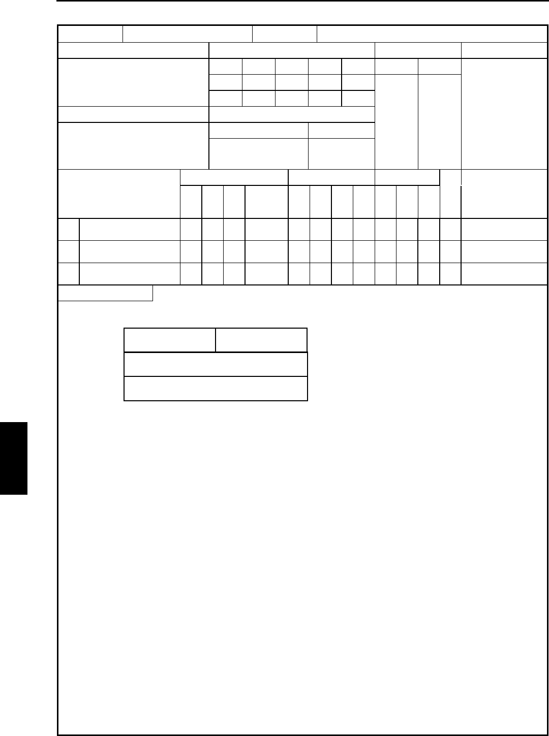
Chapter 5 Instruction Specifications
5-138
Item number FUN instructions-13 Name PWM Frequency on-duty changes
Ladder format Condition code Processing time (µs) Remark
R7F4 R7F3 R7F2 R7F1 R7F0 Average Maximum
FUN 148 (s) DER ERR SD V C
↕zzzz
Instruction format Number of steps 173
Condition Steps
FUN 148 (s) — 3
Bit Word Double word
Usable I/O XY
R,
M
TD, SS,
CU, CT WX WY
WR,
WM TC DX DY
DR,
DM
Constant
Other
sArgument (PWM output
number) {
s+1 Argument (Frequency
value) {
s+2 Argument (On-duty
value) {
Function
PWM output number: H01 to H04
**: Disable area
Frequency: 10 to 2000 (Hz)
*: If the frequency value is set to less than 10 Hz, it is
internally changed to 10 Hz. The S parameter is also
rewritten.
On-duty value:
With auto correction – Depends on the frequency used.
Without auto correction – 0 to 100 (%)
Auto correction is executed when the value corresponding to
the CPU model is specified in WRF06B.
Caution: There will be a slight error even if correction setting
is performed
•Sets the frequency value and on-duty value of the PWM output number specified by the on-duty value and the specified
frequency value.
•Sets the frequency value in Hz.
Example: To set a frequency of 1 kHz, set 1000 (H3B8) as internal output.
•Sets the on-duty value in %.
Example: To set an on-duty of 80 %, set 80 (H50) as internal output.
•When the on-duty is set to be auto-corrected, the effective range of the on-duty is calculated using the following expressions.
On-duty lower limit value (%) = Hardware delay time (µs) x Frequency used (Hz) x 10-4
On-duty upper limit value (%) = 100 − Hardware delay time (µs) x Frequency used (Hz) x 10-4
If the CPU model is EH-***DRP and the PWM output is 2 kHz,
On-duty lower limit value = 50 x 2000 x 10-4 = 10 %
On-duty upper limit value = 100 − (50 x 2000 x 10-4) = 90 %
Thus, the effective range of the on-duty will be 10 % to 90 %.
S
15 0
S + 1 Frequency values
S + 2 On-duty value
PWM number **
87
FUN 148 (s)
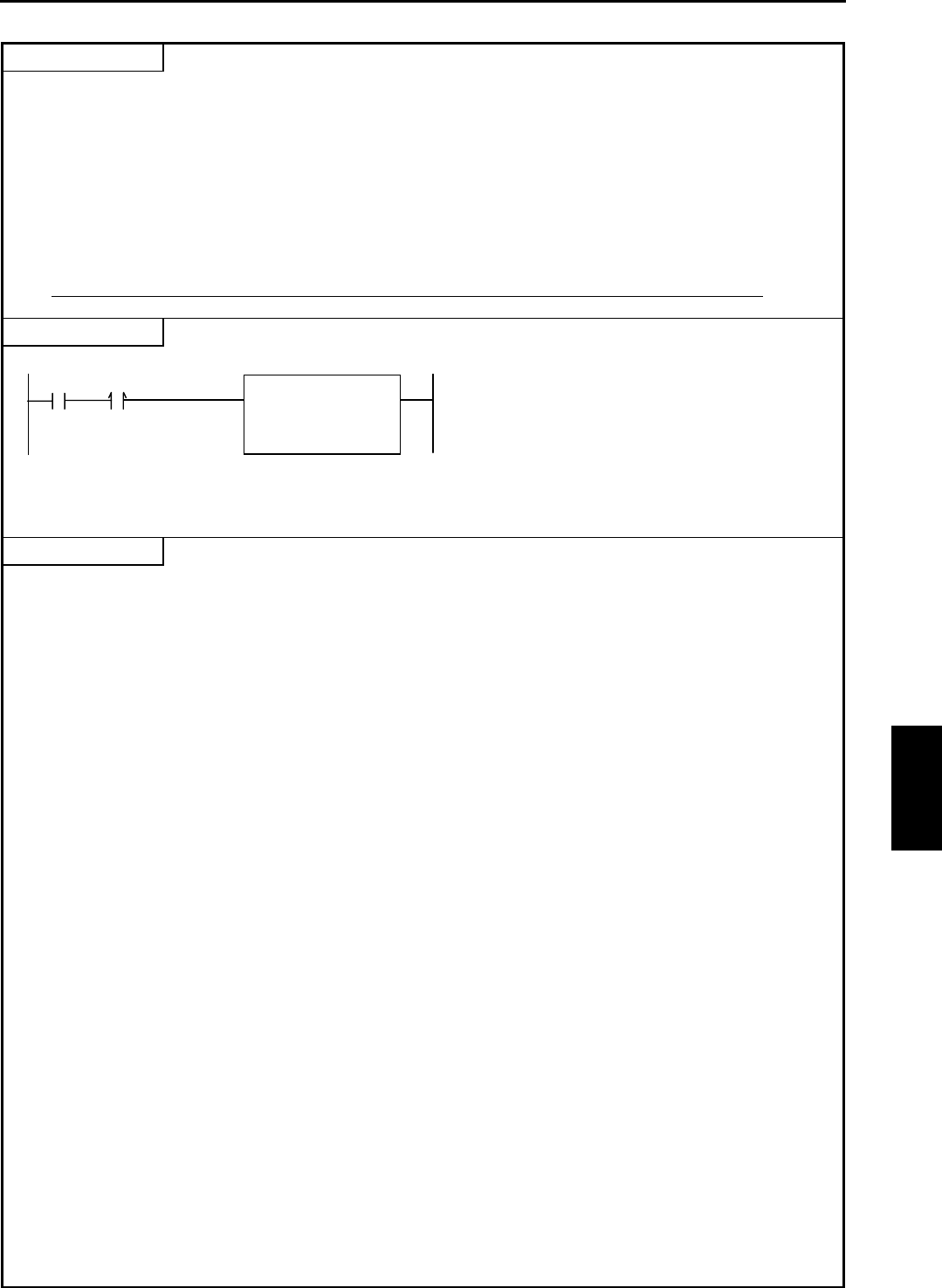
Chapter 5 Instruction Specifications
5-139
Notes
•If a value other than H01 to H04 is specified as the PWM output number, and if the on-duty value is outside the effective
range, DER will be set to “1” and no processing will be performed.
•If the external I/O corresponding to the PWM output number is set to a function other than PWM output, DER will be set to
“1” and no processing will be performed.
•The settings made using the instruction will be reflected in the special internal output (WRF072 to WRF075 and WRF076 to
WRF079). However, it is not reflected if DER becomes equal to “1.”
•The minimum frequency that can be supported is 10 kHz. If a frequency value smaller than 10 kHz is specified, it will be
changed to 10 kHz internally by the system.
•The maximum frequency that can be supported is 2 kHz. Do not set to more than 2 kHz. Operation above 2 kHz is not
guaranteed.
•If the range for S exceeds the valid range of the I/O, DER will be set to “1” and no processing will be performed.
Program example
R8 LD R8
AND DIF8
[
WR80 = H100
WR81 = 2000
WR82 = 30
FUN 148 ( WR80 )
]
DIF8 WR80 = H0100
WR81 = 2000
WR82 = 30
FUN 148 (WR80)
Program description
•Sets both the frequency and on-duty value of the PWM output No. 1 (Y100).
Sets 2000 (Hz) for the frequency and 30 (%) for the on-duty value.
FUN 148 (s)
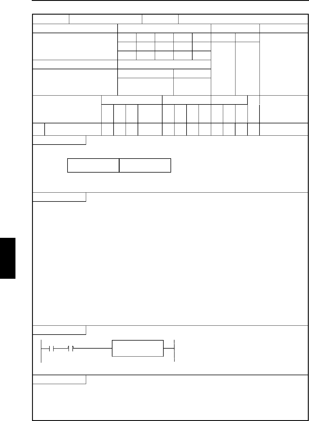
Chapter 5 Instruction Specifications
5-140
Item number FUN instructions-14 Name Pulse output control
Ladder format Condition code Processing time (µs) Remark
R7F4 R7F3 R7F2 R7F1 R7F0 Average Maximum
FUN 149 (s) DER ERR SD V C
↕zzzz
Instruction format Number of steps 149
Condition Steps
FUN 149 (s) — 3
Bit Word Double word
Usable I/O XY
R,
M
TD, SS,
CU, CT WX WY
WR,
WM TC DX DY
DR,
DM
Constant
Other
sArgument (Pulse output
number) {
Function
Pulse output number: H01 to H04
Operation instruction: H00 – Stop,
H01 - Start
•Starts pulse output of the specified pulse number and the output is stopped once the specified number of pulses are output.
Notes
•If the pulse output number is set to a value other than H01 to H04 and the pulse output number is set to “0,” DER will be set
to “1”and no processing will be performed.
•If the external I/O corresponding to the pulse output number is set to a function other than pulse output, DER will be set to
“1”and no processing will be performed.
•If the specified counter number is unable to make an output (PI/O function setting result by R7F5), DER will be set to “1”
and no processing will be performed.
•The pulse that is output with this instruction will be a pulse having a duty of 30 to 50 %. (To output a pulse having a duty
ratio of 50 %, set the value corresponding to the CPU model in the special internal output WRF06B, by referring to Section
8.1.4.)
•When pulse output is commenced with this instruction, the output control flag (R7FC to R7FF) that corresponds to the pulse
output number will turn on while the pulse is output. It will turn off when the specified number of pulses have been output.
•When the CPU is not operating, the pulse output continues/stops according to the setting of the special internal output
(output selection at R7DC stop).
•This instruction does not have an acceleration/deceleration function.
•Only pulse output stop operation can be executed for the I/O that is outputting a pulse with the acceleration/deceleration
function.
•If this instruction is executed while the backup memory is being written (R7EF=1), DER will be set to “1” and no
processing will be performed.
•The backup memory will not be written during pulse output. Be extremely careful when you change a program during RUN.
Program example
R9 LD R9
AND DIF9
[
WR9 = H101
FUN 149 ( WR9 )
]
DIF9 WR9 = H0101
FUN 149 (WR9)
Program description
•Prior to starting a pulse output operation, various settings required for the pulse output operation are reflected in the special
internal outputs, and the PI/O function setting flag (R7F5) is turned on while the CPU is being stopped.
For more details on the special internal output settings, see Chapter 8.
Starts the pulse output No. 1 (Y100) operation.
S
15 0
Pulse output number Operation instruction
FUN 149 (s)

Chapter 5 Instruction Specifications
5-141
Item number FUN instructions-15 Name Pulse frequency output setting changes
Ladder format Condition code Processing time (µs) Remark
R7F4 R7F3 R7F2 R7F1 R7F0 Average Maximum
FUN 150 (s) DER ERR SD V C
↕zzzz
Instruction format Number of steps 217
Condition Steps
FUN 150 (s) — 3
Bit Word Double word
Usable I/O XY
R,
M
TD, SS,
CU, CT WX WY
WR,
WM TC DX DY
DR,
DM
Constant
Other
sArgument (Pulse
number) {
s+1 Argument (Frequency
value) {
s+2 Argument (Number of
output pulses) {
Function
Pulse output number: H01 to H04
Change specification: H00: Sets the frequency value and
number of pulse output,
H01: Sets the frequency value
only,
H02: Sets the number of pulse
output
Frequency: 10 to 5000 (Hz)
* The maximum frequency of 5000 Hz represents the total of
all pulse output frequencies.
* If the frequency value is set to less than 10 Hz, it is
internally changed to 10 Hz. The S parameter is also
rewritten.
Number of output pulses: H0000 – HFFFF (0 to 65535)
Auto correction is executed when the value corresponding to
the CPU model is specified in WRF06B.
Caution: There will be a slight error even if correction setting
is performed.
•Pulse output is commenced at the specified frequency. Output is stopped once the number of pulses specified have been
output.
•Sets the frequency value in Hz.
Example: To set a frequency of 3 kHz, set 3000 (HBB8) as internal output.
•Sets the count for the number of output pulses.
Example: To set output of 10,000, set 10,000 (H2710) as internal output.
S
15 0
S + 1 Frequency value
S + 2 Number of pulse output
Pulse output number Change specification
FUN 150 (s)
Chapter 5 Instruction Specifications
5-142
Notes
•If the pulse output number is set to a value other than H01 to H04, DER will be set to “1”and no processing will be
performed.
•If the external I/O corresponding to the pulse output number is set to a function other than pulse output, DER will be set to
“1”and no processing will be performed.
•The minimum frequency that can be supported is 10 kHz. If a frequency value smaller than 10 kHz is specified, it will be
changed to 10 kHz internally by the system.
•If the specified frequency value is greater than 5 kHz, or even when it is 5 kHz or less, and if the total sum with other set
pulse output frequencies becomes greater than 5 kHz, DER will be set to “1” and no processing will be performed.
•If the specified frequency value is 5 kHz or less, and the total sum with other set pulse output frequencies is also 5 kHz or
less, the bit corresponding to the setting error detail WRF057 will be set to “0” and the operation enable state becomes
active.
•The settings by this instruction will be reflected in the special internal output (WRF072 to WRF075 and WRF07A to
WRF07D).
•If the range for S exceeds the valid range of the I/O, DER will be set to “1” and no processing will be performed.
•If the pulse output number is set to “0,” pulse output will not be performed even when the pulse output start (R7FC to R7FF
is set to “1” or FUN149) is set.
•If this instruction is executed for the I/O that is outputting a pulse with the acceleration/deceleration function, DER will be
set to “1” and no processing will be performed.
Program example
R10 LD R10
AND DIF10
[
WR100 = H100
WR101 = 219
WR102 = 1000
FUN 150 ( WR100 )
]
DIF10 WR100 = H0100
WR101 = 219
WR102 = 1000
FUN 150 (WR100)
Program description
•Sets both the frequency and pulse output count of the pulse output No. 1 (Y100).
Sets 500 (Hz) for the frequency and 3,000 for the number of pulse outputs.
FUN 150 (s)
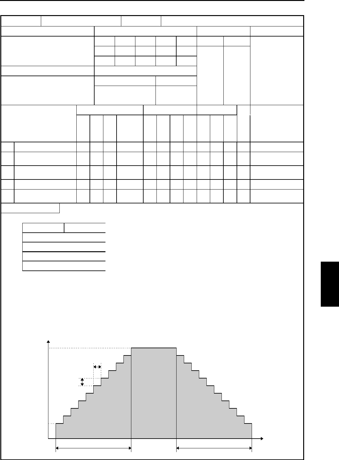
Chapter 5 Instruction Specifications
5-143
Item number FUN instructions-16 Name Pulse output with acceleration/deceleration
Ladder format Condition code Processing time (µs) Remark
R7F4 R7F3 R7F2 R7F1 R7F0 Average Maximum
FUN 151 (s) DER ERR SD V C
↕zzzz
Instruction format Number of steps 919
Condition Steps
FUN 151 (s)
Bit Word Double word
Usable I/O
XY
R,
L,
M
TD, SS,
WDT, MS,
TMR, CU,
RCU, CT WX WY
WR,
WM TC DX DY
DR,
DM
Constant
Other
s Pulse output No. {
s+1 Total No. of output
pulses {
s+2 Maximum frequency
(Hz) {
s+3 Initial frequency (Hz) {
s+4 Acceleration/deceleration
time (ms) {
Function
Pulse output No.: H01 to H04
**: Invalid area
Total No. of output pulses: H0000 to HFFFF (0 to 65535)
Maximum frequency (Hz): HA to H1388 (10 to 5000)
Initial frequency (Hz): HA to H1388 (10 to 5000)
Acceleration/deceleration time (ms): H0000 to HFFFF (0 to 65535)
This instruction outputs pulses with the acceleration/deceleration function.
It outputs pulses from the pulse output terminal set with the pulse output number s until the total number of output pulses set
with s+1 is reached.
Since the output of pulses starts from the one having the frequency set with s+3, set the parameters so that the stepping motor
and other devices will not become out of tune.
Acceleration is performed at the acceleration time set with s+4 in 10 steps until the maximum frequency set with s+2 is reached.
Deceleration is performed at the deceleration time set with s+4 until the total number of output pulses set with s+1 is reached.
The ratio of frequency change for the deceleration is the same as for the acceleration.
s
s+4
s+3
s+2
s+1
15 780
Pulse output No.
Total No. of output pulses N
Maximum frequency F (Hz)
Initial frequency F0 (Hz)
Acceleration/deceleration time T (ms)
* *
T:S+4T:S+4
Time (sec)
F:S+2
T / 10
Deceleration time
Acceleration time
9
8
7
6
5
4
3
2
0
1
10
9
8
7
6
5
4
3
2
1
F0:S+3
(F-F0) / 10
Pulse frequency (Hz)
FUN 151 (s)
Chapter 5 Instruction Specifications
5-144
Notes
When this instruction is executed, the maximum frequency is stored in the special internal output’s pulse output frequency
(WRF072 to WFR075), and the number of output pulses is stored in the special internal output’s number of output pulses
(WRF07A to WRF07D) respectively.
This instruction will not be executed if the specified pulse output is generating pulse output.
If the output that corresponds to the specified pulse output number has not been set for pulse output, DER will be set to “1” and
pulse output will not be generated.
If the total of the frequency set with this instruction and the frequency set for another pulse output exceeds 5 kHz, DER will be
set to “1” and pulse output will not be generated.
If the maximum frequency is larger than the initial frequency, DER will be set to “1” and pulse output will not be generated.
If the same value is specified for the maximum frequency and initial frequency, pulses will be output for the number of pulses
set with the maximum cycle without acceleration/deceleration.
If the maximum frequency and initial frequency are set to a value smaller than 10 Hz, the specified values will be changed to 10
Hz by the system.
If the total number of output pulses is small, deceleration will be performed without accelerating up to the maximum frequency.
In this case, the specified acceleration/deceleration time will not be used as the acceleration/deceleration time; it will be
accelerated (or decelerated) for each pulse.
For the acceleration/deceleration time, set a value equal to or larger than (1 / maximum frequency + 1 / initial frequency) x 5. If
an acceleration/deceleration time smaller than this value is specified, the specified acceleration/deceleration will not be set.
Acceleration and deceleration are performed in 10 steps, and at least one or more pulses are always output. Thus, if a small
initial frequency value is specified, an error in the acceleration/deceleration time will become large.
Pulse output at abnormal setting
•If this instruction is executed while the backup memory is being written (R7EF=1), DER will be set to “1” and no
processing will be performed.
•The backup memory will not be written during pulse output. Be extremely careful when you change a program during RUN.
Program example
Program description
Sets the required parameters in the special internal outputs at the first scan after RUN start.
At the leading edge of X00001, pulses are output starting from Y101 using the following settings: acceleration/deceleration time
of 300 (Hz), initial frequency of 500 (Hz), maximum frequency of 1000 (Hz), and number of output pulses of 4,096 pulses.
R7E3
WR0100 = H0200
WR0101 = H1000
WR0102 = 1000
WR0103 = 500
WR0104 = 300
FUN 151(WR0100)
X00001 DIF0
LD R7E3
[
WR0100 = H0200
WR0101 = H1000
WR0102 = 1000
WR0103 = 500
WR0104 = 300
]
LD X00001
AND DIF0
[
FUN 151 (WR0100)
]
Time (sec)
P
ulse frequency (Hz)
F:S+2
00
Actual acceleration time
Pulse frequency (Hz)
F:S+2
Equivalent to one pulse
Equivalent to one pulse
(F-F0) / 10
Specified deceleration time set
T:S+4
Specified acceleration time
T:S+4
Specified acceleration time
T:S+4
Actual deceleration time
F0:S+3 F0:S+3
(F-F0) / 10
FUN 151 (s)
Chapter 5 Instruction Specifications
5-145
Item number FUN instructions-17 Name BOX comment
Ladder format Condition code Processing time (µs) Remark
R7F4 R7F3 R7F2 R7F1 R7F0 Average Maximum
FUN 254 (s) DER ERR SD V C
* (BOXC (s) ) zzzzz
Instruction format Number of steps
Condition Steps
FUN 254 (s) 3
* (BOXC (s) )
Bit Word Double word
Usable I/O XY
R,
M
TD, SS,
CU, CT WX WY
WR,
WM TC DX DY
DR,
DM
Constant
Other
sArgument (dummy
constant) {
Function
•This instruction does not perform any operations. It is used to print comments on the right side of the calculation box in
conjunction with the Ladder Editor.
•A comment can contain a maximum of 32 characters.
* ( ) indicates the display when the Ladder Editor is used.
Item number FUN instructions-18 Name Memo comment
Ladder format Condition code Processing time (µs) Remark
R7F4 R7F3 R7F2 R7F1 R7F0 Average Maximum
FUN 255 (s) DER ERR SD V C
* (MEMC (s) ) zzzzz
Instruction format Number of steps
Condition Steps
FUN 255 (s) 3
* (MEMC (s) )
Bit Word Double word
Usable I/O XY
R,
M
TD, SS,
CU, CT WX WY
WR,
WM TC DX DY
DR,
DM
Constant
Other
sArgument (dummy
constant) {
Function
•This instruction does not perform any operations. It is used to print comments on the right side of the calculation box in
conjunction with the Ladder Editor.
•A comment can contain a maximum of one screen (66 characters × 16 lines).
* ( ) indicates the display when the Ladder Editor is used.
FUN 254 (s)
FUN 255 (s)

Chapter 5 Instruction Specifications
5-146

Chapter 6 I/O Specifications
6-1
Chapter 6 I/O Specifications
Table 6.1 lists the input/output classifications and input/output point types that can be used with the MICRO-EH
Table 6.1 Usable I/O classifications and point types
10-point
type
14-point
type
23-point
type
28-point
type
Item
Function
Symbol
Size
10/16
Name Number of
points
Number of
points
Number of
points
Number of
points
1 External I/O X B 10 Bit external input 6 points 8 points 13 points 16 points
WX W 16 Word external input 1 word 1 word 1 word 2 words
DX D 16 Double-word external input
Y B 10 Bit external output 4 points 6 points 10 points 12 points
WY W 16 Word external output 1 word 1 word 1 word 1 word
DY D 16 Double-word external output
Analog input WX W 16 Analog input - - 2 words -
Analog output WY W 16 Analog output - - 1 word -
Counter input X B 10 High-speed counter input 3 points 4 points 4 points 4 points
Interrupt input X B 10 Interrupt input total total total total
Counter
output
Y B 10 High-speed counter synchronized
output
3 points 4 points 4 points 4 points
External I/O*
Pulse/PWM
output
Y B 10 Pulse output
PWM output
3 point 4 points 4 point 4 points
2 Bit R B 16 Bit internal output 1984 points
R B 16 Bit special internal output 64 points
Word WR W 16 Word internal output 4096 words
DR D 16 Double-word internal output
WR W 16 Word special internal output 512 words
DR D 16 D.-word special internal output
Sharing of M B 16 Bit internal output 16384 points
bit / word WM W 16 Word internal output 1024 words
Internal I/O
DM D 16 Double-word internal output
3 Edge detection DIF B 10 Rising edge 512 points
DFN B 10 Falling edge 512 points
Master control MCS B 10 Master control set 50 points
MCR B 10 Master control reset
Timer counter TD B 10 On delay timer
SS B 10 Single-shot timer
CU B 10 Up counter
CTU B 10 Up-down counter up input
CTD B 10 Up-down counter down input
Others
CL B 10 Clear progress value
Timer 256 points (0.01 s timer has only 0 to 63)
Counter 256 points (The same area as the timer is used.)
(The same timer counter number cannot be used more
than once.)
*: The external I/O, counter I/O, interrupt input, pulse/PWM outputs use the same area by specifying the operation I/O
operation mode (WRF070). See Chapter 8 for further information.
Note: The MICRO-EH does not support CPU link area (L/WL).
Note: B and W in the Size column represent bit and word (16 bits), respectively.

Chapter 6 I/O Specifications
6-2
6.1 I/O Assignment
I/O assignment and I/O address are listed below.
Table 6.2 I/O assignment and I/O address
Type I/O assignment 10-point
type
14-point
type
23-point
type
28-point
type
Slot 0 : X48 X0-5 X0-7 X0-12 X0-15
Slot 1 : Y32 Y100-103 Y100-105 Y100-109 Y100-111Digital
Slot 2 : Empty - - - -
Slot 3 : X4W - - WX30-31 -
Basic
Analog Slot 4 : Y4W - - WY40 -
- X1000-1007 / 1015 (14 / 28 pts.)
Digital Unit 1 / Slot 0 : B1/1
- Y1016-1021 / 1027 (14 / 28 pts.)
- WX101-104 (WX100 is for command function under development)
Exp.1
Analog Unit 1 / Slot 0 : FUN0
- WY106-107 (WY105 is for command function under development)
- X2000-2007 / 2015 (14 / 28 pts.)
Digital Unit 2 / Slot 0 : B1/1
- Y2016-2021 / 2027 (14 / 28 pts.)
- WX201-204 (WX200 is for command function under development)
Exp.2
Analog Unit 2 / Slot 0 : FUN0
- WY206-207 (WY205 is for command function under development)
- X3000-3007 / 3015 (14 / 28 pts.)
Digital Unit 3 / Slot 0 : B1/1
- Y3016-3021 / 3027 (14 / 28 pts.)
- WX301-304 (WX300 is for command function under development)
Exp.3
Analog Unit 3 / Slot 0 : FUN0 - WY306-307 (WY305 is for command function under development)
- X4000-4007 / 4015 (14 / 28 pts.)
Digital Unit 4 / Slot 0 : B1/1
- Y4016-4021 / 4027 (14 / 28 pts.)
- WX401-404 (WX400 is for command function under development)
Exp.4
Analog Unit 4 / Slot 0 : FUN0
- WY406-407 (WY405 is for command function under development)
Chapter 6 I/O Specifications
6-3
6.2 External I/O Numbers
When starting an operation of the MICRO-EH, a user program is executed (scanned) after the input refresh processing
(receiving external input data) is performed. Operations are performed according to the contents of the user program, and
the next input refresh processing and output refresh processing (operation results are reflected in the external output) are
performed. After that, the next user program is executed (scanned). This series of operations is continually repeated until
the operation is stopped or until a problem occurs in which the operation can no longer continue.
When the operation is stopped or if a problem interrupting the operation occurs, the CPU performs output refresh
processing making all output data as off data and then stops the operation, regardless of the execution status of the user
program.
Figure 6.1 shows a diagram outlining this series of operations.
Input refresh processing Input refresh processing Output refresh processing
Execute (scan) user program System processing
RUN start
RUN stop
Output refresh processing (off data)
Execute (scan) user program
Time
Time
Figure 6.1 Overview of user program execution and refresh processing
The user programs are executed in sequence, normally beginning with the program in the beginning of the scan area till
the last program, or until the END instruction. Then, I/O data is refreshed prior to the execution of the next user program.
As shown above, external I/O data is updated in batch mode in the refresh processing after the user program is executed.
If it is necessary to update (refresh) the I/O data while the user program is being executed, use the refresh instruction.
When designing a system, take into account the above refresh operation from when the input data is received and
operated until output data is obtained.
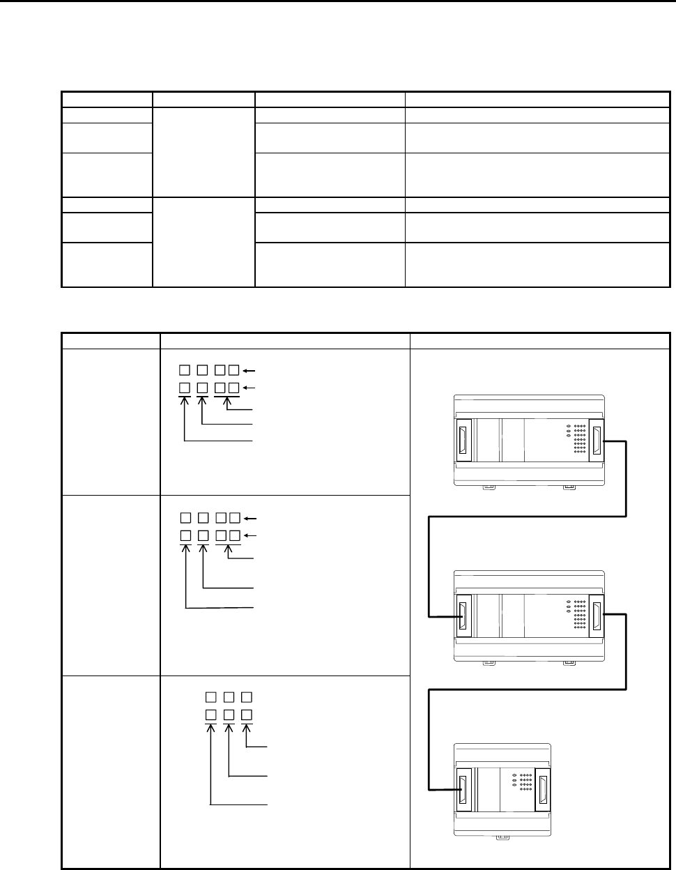
Chapter 6 I/O Specifications
6-4
The following explains the external I/O assignment. The external I/O numbers for the MICRO-EH system are expressed
with the following conventions.
Table 6.6 List of external I/O classification and data type
Classification I/O classification Data type Remarks
X External input Bit type Corresponds to the signal of each terminal block.
WX Word type (16-bit) Data in the range 0 to 15 is batch processed.
16-bit synchronicity guaranteed.
DX Double-word type (32-bit) Two word data are batch expressed.
Lower 16-bit and upper 16-bit synchronicity are
not guaranteed.
Y External output Bit type Corresponds to the signal of each terminal block.
WY Word type (16-bit) Data in the range 0 to 15 is batch processed.
16-bit synchronicity guaranteed.
DY Double-word type (32-bit) Two word data are expressed as one batch.
Lower 16-bit and upper 16-bit synchronicity are
not guaranteed.
Table 6.7 List of I/O number conventions for external I/O
Data type Numbering convention Example
Bit type (basic)
X
Y
Input
Output
Bit number
Slot number (X:0 Y:1)
Unit number (0)
Bit type
(expansion) X
Y
Input
Output
Bit number
(X:00-07/15 Y:16-21/27)
Slot number (0)
Unit number (1-4)
Word type
(basic/expansion) WX
WY
Word number
Slot number
Unit number (1-4)
X0~X12, WX30,WX31
Y100~Y109, WY40
X1000~X1015
Y1016~Y1021
WX201~WX204
WY206, WY207
EH-A23DRP
EH-A28EDR
EH-A6EAN (Analog exp.)
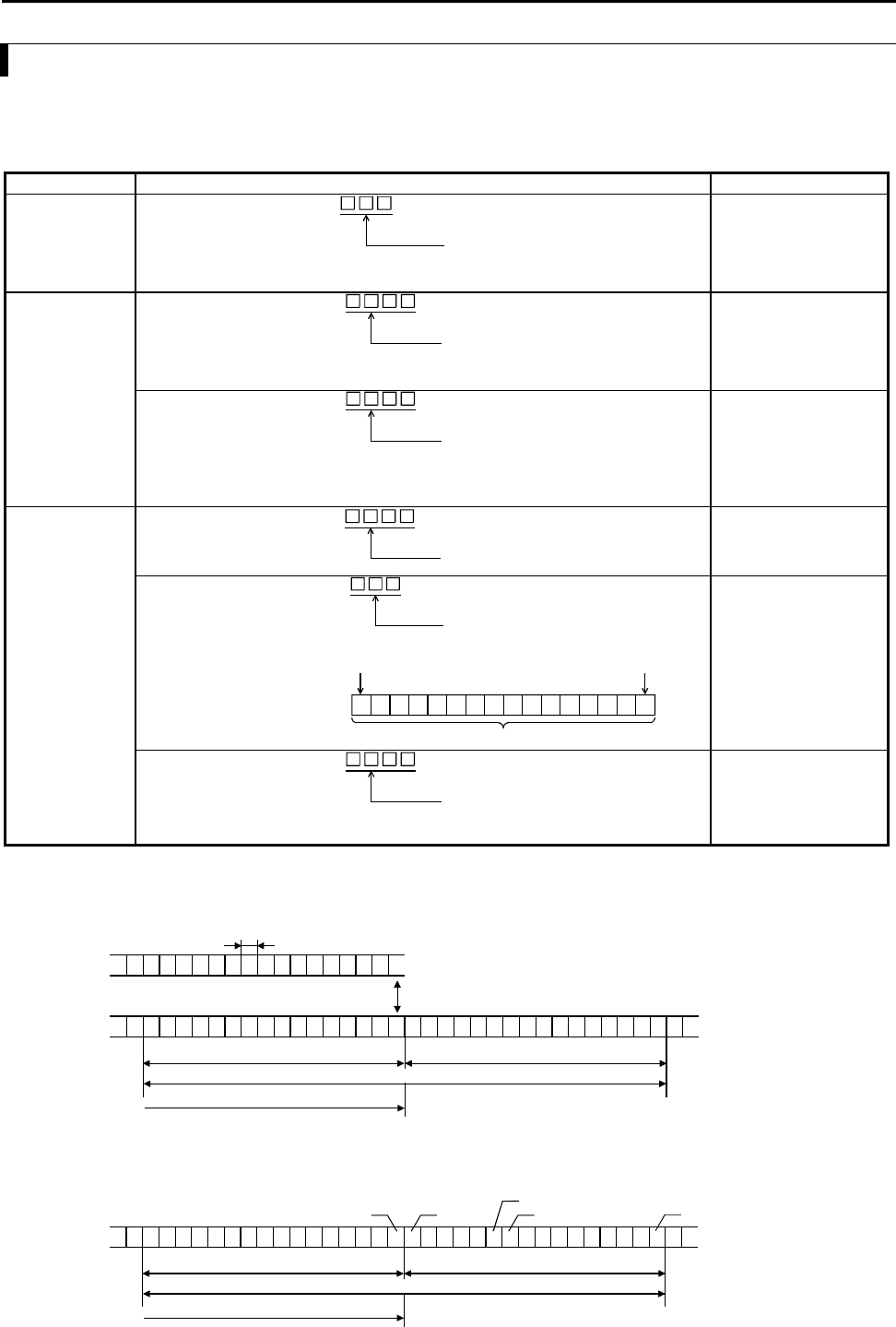
Chapter 6 I/O Specifications
6-5
6.3 Internal Output Numbers
Memory is available as an internal output area in the CPU module. There are three areas: bit dedicated area (R), word
dedicated area (WR), and bit/word shared area (M/WM).
Table 6.8 List of I/O number conventions for external I/O
Data type Numbering convention Example
Bit-dedicated
type
R
Normal area H000 to H7BF
Special area H7C0 to H7FF
Both are expressed as hexadecimals.
R0
R105
R23C
R7E7
Word dedicated
type
<Word> WR
Normal area H0000 to
Special area HF000 to
Both are expressed as hexadecimals.
WR0
WR11
WR123
WRF004
<Double word> DR
Normal area H0000 to
Special area HF000 to
Both are expressed as hexadecimals.
Expresses WR for 2 words in continuation.
DR0
DR11
DR123
DRF004
Bit/word shared
type
<Bit>
M
H0000~
M0
M11
M123
<Word> WM
H000~
M120F ........... M1200
WM120
WM0
WM11
WM123
<Double word> DM
H0000 to
Expresses as hexadecimals.
Expresses DM for 2 words in continuation.
DM0
DM11
DM234
•Internal outputs R, WR and DR are completely separate areas. Bit-based operations cannot be performed in the WR.
(Example) Relationships among R100, WR10, and DR10
DR11
R100
WR11 WR10
DR10
WR/DR area Another area
R area
•Because internal outputs M, WM and DM share the same area, bit-based operations are allowed.
(Example) Relationships among M100, WM10, and DM10
DM10
M11F ....... M10FM110
DM11
M109
M10A
M100
.......
WM11 WM10
Chapter 7 Programming
7-1
Chapter 7 Programming
7.1 Memory Size and Memory Assignment
Table 7.1. Lists the programming specifications for the MICRO-EH.
Table 7.1 Programming specifications
No. Item 10/14-point type 23/28-point type
1 Program size 3 k steps (3072 steps)
2 Instruction size 32 bits/1 step
3 Memory specification SRAM Backup with a battery is not possible
since a battery cannot be installed.
Backup is possible by installing the
battery.
FLASH Backup using flash memory is possible.
4 Programming language H-series ladder/instruction language
5 Program creation Created with H-series programming devices
6 Program modification During STOP Can be done as desired from the programming devices.
During RUN Can be done using the modify during RUN operation (except control instructions).
Control instructions can be changed with special operations. *1
(When a change is made during RUN, control operation stops while the program
is being modified.).
7 Program protection Programs can only be modified when write is enabled. (The enable status is
automatically controlled by the programming device).
8 Password A password can be set from the programming device (the program cannot be
displayed when setting the password. The programs can be downloaded to the
programming device).
9 Check function A sum check function for the program is always executing. An address check with
the I/O assignment table is executed when RUN operation starts.
10 Program name The program names are set from the programming device and stored along with
the programs.
*1: Refer to the peripheral unit manual for details.
Notes:
• Comment data that has been created with the peripheral unit is not stored in the CPU.
• Save the user programs to a floppy disk or other media for backup.
• If a program exceeding 3072 steps is created by setting 4 K steps in the LADDER EDITOR, no error occurs in the LADDER
EDITOR, but a “writing outside memory range” error will occur when writing the program to the CPU.
• Unlike the conventional H series, the MICRO-EH series backup user programs in the FLASH memory.
In order to shorten the program transfer time, the user programs are transferred once to the operation execution memory, at which
point the transfer is completed. The backup to the FLASH memory is performed afterward; therefore, be sure to turn off the
power to the main unit after approximately two minutes have passed since the program transfer. If the power is turned off within
two minutes, a user memory error (31H) may occur. Note that the transfer completion to the FLASH memory can be confirmed
by the special internal output (R7EF).

Chapter 7 Programming
7-2
7.2 Programming Devices
The following methods are used to create the user programs.
Table 7.2 Programming methods
No. Programming device used Concept of operation Remarks
1 Personal computer software
(LADDER EDITOR, etc.)
[For off-line/on-line operation]
Creates an I/O assignment table, inputs the program to be
created, and transfers the program to the CPU in online
mode.
[For direct operation]
As each program is entered one by one, it is directly
written to the CPU.
Change operation can be performed during RUN
operation.
Note: This mode is not available for Windows
version.
[During on-direct operation]
When programs are input one by one, the input programs
are written into the CPU’s memory and personal
computer’s memory.
Change operation can be performed during RUN
operation.
Note: To enter the on-direct mode, match the contents in
the CPU’s memory and personal computer’s
memory.
• I/O assignment information
can be read.
• Initialize the CPU when
starting up for the first time
after the unit is unpacked or
when a battery error occurs.
2 Dedicated programming
console (GPCL01H, etc.)
[For off-line/on-line operation]
Creates an I/O assignment table, inputs the program to be
created, and transfers the program to the CPU in online
mode.
[For direct operation]
As each program is entered one by one, it is directly
written to the CPU.
Change operation can be performed during RUN
operation.
Note: This mode is not available for Windows
version.
[During on-direct operation]
On-direct operation cannot be performed.
Portable graphic programmers and instruction language programmers can not be used.
Chapter 7 Programming
7-3
7.3 Programming Methods
The following shows the system configuration using a personal computer and the procedures for creating a user program
using personal computer software. Please note that cables differ depending on the personal computer and software used.
Table 7.3 System configuration using a personal computer
No. Personal computer
software used DOS/V PC PC9800 series personal computer
1 LADDER EDITOR
(Windows version)
DOS/V PC
(Windows 95/98/NT)
Install
LADDER EDITOR for
Windows (HLW-PC3,
HLW-PC3E) system disks
(Japanese, English)
Install
PC9800 series PC
(Windows® 95/98/NT)
LADDER EDITOR for
Windows® (HLW-PC3)
system disks (Japanese)
CPU setting Specify H-302.
Memory assignment Specify RAM-04H (4 K memory).
Cable (MICRO-EH side) EH-RS05 EH-VCB02 EH-RS05
Cable
(personal computer side) WVCB02H WPCB02H
10-point type There are no DIP switches (fixed to 4800 bps).
DIP SW1234
ON OFF ON OFF 38.4 kbps
ON OFF OFF OFF 19.2 kbps
OFF OFF ON OFF 9600 bps
Port 1
*1, *2 14/23/28-point type Status
OFFOFFOFFOFF4800 bps
Same as left
10/14-point type Port 2 does not exist.
Port 2 23/28-point type
Cannot be connected with the above configuration since the RS-422/485 are used (RS-
232C/422 converters are required.)
Set the transmission speed in the special internal output (WRF03D).
2 LADDER EDITOR
(DOS version)
D
OS/V PC
(
MS-DOS®)
Install
LADDER EDITOR DOS
version (HL-AT3E)
system disks (English)
Install
P
C9800 series
P
C (MS-DOS®)
LADDER EDITOR
DOS version (HL-PC3)
system disks (Japanese)
CPU setting Specify H-302.
Memory assignment Specify RAM-04H (4 k memory).
Cable (MICRO-EH side) EH-RS05
Cable
(personal computer side)
EH-VCB02 PCCB02H
10-point type There are no DIP switches (fixed to 4800 bps).
DIPSW1234
Port 1
*1, *2 14/23/28-point type Status OFF OFF OFF OFF 4800 bps Same as left
10/14-point type Port 2 does not exist.
Port 2 23/28-point type
Cannot be connected with the above configuration since the RS-422/485 are used (RS-
232C/422 converters are required.)
Set the transmission speed in the special internal output (WRF03D).
*1: Settings of the port 1 can be changed when the DR signal is off. When the DR signal is on, the setting is fixed.
*2: Set the port 1 to the transmission control procedure 1 by the special internal output (WRF01A). (The default is the transmission
control procedure 1.)
Note: Refer to the manual of the applicable software on how to install and operate each software (LADDER EDITOR).
Chapter 7 Programming
7-4
Table 7.4 List of procedures for creating a program
Create new program Modify Test operation, adjustment
Item Off-line Off-line On-line On-direct
Out-line of opera-ting procedure
OK
N
G
Start
Select off-line
Initialize PLC
CPU type: Specify H-302
Memory type: Specify RAM-04H
Create I/O assignment
Create program
Program check
Save in FD, etc.
End
OK
N
G
Start
Select off-line
Regenerate from FD, etc.
When utilizing a program created
in another H-series
CPU type: Specify H302
Memory type: Specify RAM-04H
Modify I/O assignment
Modify program
Change the name and
save in FD, etc.
Program check
End
OK
OK
OK
NG
NG
*1
Start
Select on-line
Regenerate from FD, etc.
Initialize the CPU when
running it for the first
time(right after purchase, etc.)
(PLC → CPU)
CPU error check
Conduct test operation
Operation check
To modificatio
n
End
Transfer program
OK
OK
N
G
Start
Select on-line
Transfer program
(CPU → PLC)
Select on-direct
Conduct test operation
Modify program (modify
during RUN, etc.)
Operation check
Enter in FD, etc.
End
Situation
When creating a new
program
When modifying a program When transferring a created
program to the CPU for the
first time
When modifying a program
during test operation
Point
A program can be created
without executing MICRO-
EH.
When using a program that
was used in another H-series,
specify H-302 as the CPU
type.
When performing CPU error
check, make sure the I/O
assignment matches the
loaded module. (The loading
read function can be used to
match them forcibly.)
To enter the on-direct mode,
match the contents in the
CPU’s memory and personal
computer’s memory. The
modified contents will be
reflected in both the
computer memory and CPU
memory.
*1: Set the flow size to 0 for memory assignment.
If a program transfer is performed by specifying the flow size, the message “Cannot execute: Operation error” is displayed, and
a peripheral unit remain as WRITE occupied. In this case, either cancel the occupy state from LADDER EDITOR of the
peripheral unit or by re-entering the CPU power.
Chapter 7 Programming
7-5
The user program is managed in circuit units. One circuit can describe nine contact points (a-type contact point or b-type
contact point) and seven coils as shown in the figure below.
Figure 7.1 Size of one circuit
Or, one relational box can be described using the width of three contact points. The relational box can be considered as an
a-type contact point that turns on when the conditions in the box are established (Figure 7.2).
Figure 7.2 Example when using a relational box
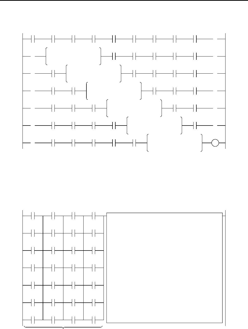
Chapter 7 Programming
7-6
In addition, if loop symbols are used, a circuit containing up to 57 contact points and one coil can be entered within seven
lines.
However, an OR circuit cannot be input after a loop.
*
*
*
*
*
*
*
*
*
*
*
*
Figure 7.3 Example when using loop symbols
A processing box can be placed at the coil position. The processing instructions, application instructions, control
instructions, transfer instruction and fun instructions can be described in a processing box. A maximum of 19 instructions
can be described in one processing box. The processing box is executed when the conditions in the contact section to be
connected directly in advance is established. The processing box is not executed if the condition is not established.
See the chapter on the “Instruction Specifications” for details on each instruction.
WR0 = WR0 + WR1
WR1 = WR1 * 3
WR2 = WR2 / 4
WR0 = WX0 AND HFF00
.
.
.
.
.
.
.
.
.
.
.
.
.
.
.
.
Up to a maximum of 19 lines
A maximum of 4 lines can be described
Figure 7.4 Example when using a processing box
Note: For the LADDER EDITOR for Windows, a processing box can be displayed in one contact point width, so a circuit of nine
contact points and one processing box can be entered.
For more details, refer to the user's manual for the LADDER EDITOR for Windows.
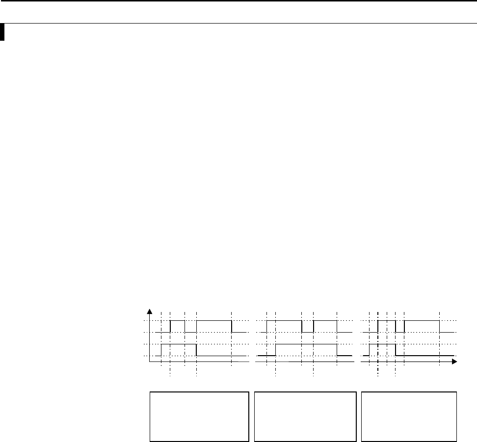
Chapter 7 Programming
7-7
7.4 Program Transfer
The MICRO-EH stores the user programs written from the peripheral units in the execution memory (RAM). Then, it
transfers the user programs to the FLASH memory (backup memory) utilizing the idle time of the MPU in the internal
area of the MICRO-EH. This is performed regardless of operation status of the CPU. Therefore, the programs may not be
written into the backup memory (FLASH memory) even though the peripheral units display that program transfer has
been completed. If the power is turned off before the programs are written to the FLASH memory, the customer’s
programs may be lost.
In order to prevent such crisis, it is necessary to monitor the Backup Memory Writing Progress Flag (R7EF) after the
programs are transferred. When this bit special internal output is ON, it indicates that the data (programs, etc.) are being
transferred to the backup memory. When is it OFF, it indicates that the data is not being written to the backup memory.
Turning off the power after making sure that the Backup Memory Writing Progress Flag (R7EF) turns off after the
program is transferred from the peripheral unit to the MICRO-EH will ensure that the program is backed up properly.
(The transfer to the backup memory takes approximately two minutes.)
If a new program is written from a peripheral unit while a user program is being transferred to the backup memory
(FLASH memory), the user program transfer to the backup memory will be stopped and the new program will be
transferred to the backup memory. Therefore, the program that is stored in the backup memory will be the program that is
written last.
In addition to the user programs, the settings to be stored in the special internal outputs can be transferred to the backup
memory. The transfer of the special internal outputs for various settings (Note 1) can be executed by turning ON the
Memory Request for Various Settings Flag (R7F6). As with the transfer of the user programs, the Backup Memory
Writing Progress Flag (R7EF) will be turned ON during this transfer.
Figure 7.5 below shows the operation of the Backup Memory Writing Progress Flag (R7EF) during the backup of the
special internal output for various settings and the backup of the user programs. Note that when one is being transferred,
the next transfer will not start until the current transfer is complete.
1] R7F6 ON due to forced set or reset
2] Special internal output transfer start for various settings
3] Special internal output transfer end for various settings
4] Write from the peripheral unit is complete.
5] User program transfer start
6] User program transfer end
Figure 7.5 Operation of the bit special internal output when backup memory is being accessed
Note:
•The backup memory cannot be written during pulse output. If a program is changed during RUN with respect to the CPU
during pulse output, turn off the power supply approximately two minutes after pulse output stops.
•Pulses cannot be output while the backup memory is being written. Commence pulse output once again after the Backup
Memory Writing Progress Flag turns off.
6
]
6
]
4
]
4], 5] 3]
3
]
2]
1
]
5
]
6
]
1]
3
]
2] 2]
1
]
R7F6
R7EF
Backup memory writing
progress flag
Special internal output
write request for various
settings
When there is no conflict
between the user program
write and the setting memory
request of the special internal
out
p
ut
When a setting memory
request of the special internal
output is generated during the
transfer of the user program
When a user program write
is generated during the
transfer of the special
internal output
4], 5]

Chapter 7 Programming
7-8
Note 1) The following lists the special internal outputs for various settings that can be transferred to the backup memory by the
Memory Request for Various Settings Flag (R7F6).
Table 7.5 List of special internal outputs that can be stored
No. Special internal output
that can be stored Function
1 WRF01A Dedicated port 1 Communication settings
2 WRF03C Dedicated port 1 Modem timeout time
3 WRF03D Dedicated port 2 Communication settings
4 WRF06B Pulse/PWM automatic correction settings
5 WRF06C Potentiometer 1 Filtering time
6 WRF06D Potentiometer 2 Filtering time
7 WRF06E Analog input type selection
8 WRF06F Phase counting mode
9 WRF070 I/O operation mode
10 WRF071 I/O detailed function settings
11 WRF072
12 WRF073
13 WRF074
14 WRF075
Output frequency
On-preset value
15 WRF076
16 WRF077
17 WRF078
18 WRF079
On-duty value
Off-preset value
19 WRF07A
20 WRF07B
21 WRF07C
22 WRF07D
Pre-load value
Pulse output value
23 WRF07E Input edge
24 WRF07F Input filtering time
Chapter 8 High-speed counter, PWM / Pulse train output and Analogue I/O
8-1
Chapter 8 High-speed counter, PWM / Pulse train
output and Analogue I/O
The MICRO-EH operates in four operation modes. By selecting the proper operation mode, input/output points can be assigned to
the counter input, interrupt input, pulse output, and PWM output functions, instead of the normal input/output function.
The 14-point type model or higher are equipped with two potentiometers. The values of internal outputs can be changed externally
using these potentiometers, without peripheral units.
The 23-point type model is equipped with two points of analogue input and one point of analogue output.
This chapter explains how to set various functions mentioned above, together with simple usage examples.
8.1 Input/Output Function
The normal input/output points can not only be used as they are, but can also be assigned special functions. In order to
assign these special functions, it is necessary to select the right operation mode; the following briefly explains the
procedure for selecting the operation modes. Refer to the section corresponding to each item for the details.
8.1.1 Initial Setting for Special Input/Output Function
Figure 8.1 shows a flowchart for the setting procedures.
First, select an operation mode. There are 5 operation modes, mode 0 to 3 and 10. By selecting an operation mode the
input number to be used for high-speed counter input and the type of counter is determined, along with the output number
for the corresponding output.
Next, the desired input/output function for each point of input/output should be selected, because the function assigned to
input/output varies depending on the operation mode selected.
Lastly, set the operating conditions for each input/output function selected.
Furthermore, performing the settings mentioned above does not in itself make the settings valid for the actual operation.
The settings become valid only after turning on the special internal output for individual setting (R7F5). After making the
settings valid, it is possible to make changes for each function using the special internal output for individual setting.
Turning the special internal output (R7F6) on also stores the settings performed above in the FLASH memory. From the
next time the power supply is turned on, the settings stored in the FLASH memory are automatically read; it is not
necessary to perform the settings every time.
Figure 8.1 Flow of operation mode setting procedure
Set the number 0 to 3 corresponding to the mode you want to set in WRF070.
Refer to Table 8.1 for the details of each mode.
Note 1) If nothing is set, the settings stored in the FLASH memory become valid.
Note 2) If a number larger than 4 is set, mode 0 will be selected.
Note 3) After the settings are stored in the FLASH memory, it is not necessary to perform the settings
after step 1] from the next time.
Set the function of each input/output terminal in WRF071.
Refer to the section about detailed function settings for the details.
Note 4) If nothing is set, the initial value will become 0.
Set the operating conditions for each function in WRF072 to WRF07E.
Refer to the section about detailed operating condition settings for the details.
Note 5) If nothing is set, the initial value will become 0.
The settings performed in steps 1] to 3] become valid by turning R7F5 on.
Note 6) The settings performed in steps 1] to 3] do not become valid unless R7F5 is turned on while
output is turned off.
Moreover, if R7F5 is turned on while the CPU is running, the settings do not become valid
even though R7F5 is turned on. The settings become valid at the point when the CPU is
stopped.
The settings performed in steps 1] to 3] are stored in the FLASH memory by turning R7F6
on.
It is not necessary to perform the settings again when the power supply is turned on for the
next time.
Note 7) If R7F6 is not turned on, the settings will be changed to the ones stored in the FLASH
memory when the power supply is turned on for the next time (if nothing is stored in the
FLASH memory, the initial values will be set).
Note 8) When the CPU is operating, the settings are not stored in the FLASH memory by turning
R7F6 on.
Note 9) R7EF turns on while the settings are transferred to the FLASH memory. If the power supply
to the main unit is turned off while R7EF is on, the settings are not properly stored in the
FLASH memory; there is a possibility that the parameter settings are initialized when the
power supply is turned on for the next time.
1] Set the operation mode
3] Set the operating conditions
for each function
6] Store the settings in the memory.
2] Set input/output terminal
5] Change
individual setting
4] Make the settings valid

Chapter 8 High-speed counter, PWM / Pulse train output and Analogue I/O
8-2
8.1.2 Operation Mode
Select one mode from the 5 modes shown in Table 8.1 (mode 10 described in following pages.) and set the mode number
in the special internal output WRF070 when the CPU is in STOP status.
*1: If parameter in WRF070 is not saved by R7F6, the value will be 0 at the next power on.
*2: The operation mode setting can be changed only when CPU is in STOP status.
Each input and output terminal setting is configured in WRF071.
Table 8.1 Operation mode list
Mode 0 Mode 1 Mode 2 Mode 3
Standard Single-phase counter ×2 Single-phase counter ×42-phase counter ×1,
Single-phase counter ×1
X0 Standard input Counter input 1 Counter input 1 Counter input 1A
Standard input Counter preload 1 Counter preload 1 Counter preload 1
Interrupt input 1 Counter strobe 1 Counter strobe 1 Counter strobe 1
X1
Standard input *6 Standard input *6 Standard input *6
X2 Standard input Counter input 2 Counter input 2 Counter input 1B
Standard input Counter preload 2 Counter preload 2 Counter input (marker) 1Z
Interrupt input 2 Counter strobe 2 Counter strobe 2
X3
Standard input *6 Standard input *6
X4 Standard input Standard input Counter input 3 Standard input
Standard input Standard input Counter preload 3 Standard input
Interrupt input 3 Interrupt input 3 Counter strobe 3 Interrupt input 3X5
Standard input *6 Standard input *6
X6 Standard input *3 Standard input *3 Counter input 4 *3 Counter input 4 *3
Standard input *3 Standard input *3 Counter preload 4 *3 Counter preload 4 *3
Interrupt input 4 *3 Interrupt input 4 *3 Counter strobe 4 *3 Counter strobe 4 *3
X7
Standard input *6 Standard input *6 Standard input *6
Standard output Counter output 1 Counter output 1 Counter output 1
PWM output 1 Standard output *6 Standard output *6 Standard output *6
Y100
Pulse output 1
Standard output Counter output 2 Counter output 2 Standard output
PWM output 2 *5 Standard output *6 Standard output *6 PWM output 2 *5
Y101
Pulse output 2 *5 Pulse output 2 *5
Standard output Standard output Counter output 3 Standard output
PWM output 3 *5 PWM output 3 *5 Standard output *6 PWM output 3 *5
Y102
Pulse output 3 *5 Pulse output 3 *5 Pulse output 3 *5
Standard output Standard output Counter
output 4 *4
Standard
output
Counter
output 4 *4
Standard
output
PWM output 4 *5 PWM output 4 *5 Std. output *6 PWM out 4 *5 Std. output *6 PWM out 4 *5
Y103
Pulse output 4 *5 Pulse output 4 *5 Pulse out 4 *5 Pulse out 4 *5
*3: Modes 0 to 3 can be set regardless of the type of CPU however, note that the 10-point type does not have X6
and X7.
*4: It is only possible to select either Standard output, PWM output, or pulse output for the 10- point type CPU. (A
counter corresponding output cannot be set because there is no counter input that can correspond to it.)
*5: It is possible to set for the relay output type, but the expected output waveform cannot be obtained. Moreover,
care must be taken because it may cause an relay error.
*6: This assignment is supported by Ver.1.11 (WRF051=H0111) or newer.
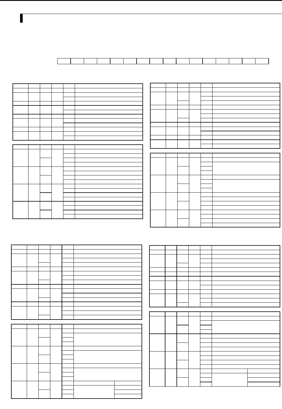
Chapter 8 High-speed counter, PWM / Pulse train output and Analogue I/O
8-3
8.1.3 Input/Output Setting
Configure each I/O setting in the special internal output (WRF071) and make it effective by setting R7F5 ON in CPU
STOP status. This information is normally reset at every power on, but this can be saved in the FLASH memory by
setting R7F5 ON after that.
Bit: 1514131211109876543210
WRF071: abcdefghi jklmnop
Initial value: 0000000000000000
Figure 8.2 Special internal output for setting detailed function
Mode 0
Name Bit Value Bit Value Function
X0----Standard input (Fixed)
0 Standard input
X1 a 0 b 1 Interrupt input
X2----Standard input (Fixed)
0 Standard input
X3 c 0 d 1 Interrupt input
X4----Standard input (Fixed)
0 Standard input
X5 e 0 f 1 Interrupt input
X6----Standard input (Fixed)
0 Standard input
X7 g 0 h 1 Interrupt input
Name Bit Value Bit Value Function
0 Standard output
01 PWM output
0 Pulse output
Y100 i
1
j
1-
0 Standard output
01 PWM output
0 Pulse output
Y101 k
1
l
1-
0 Standard output
01 PWM output
0 Pulse output
Y102 m
1
n
1-
0 Standard output
01 PWM output
0 Pulse output
Y103 o
1
p
1-
Mode 1
Name Bit Value Bit Value Function
X0 - - - - Counter input (Fixed)
0 Counter preload
01 Counter strobe
X1 a
1
b
0 Standard input *1
X2 - - - - Counter input (Fixed)
0 Counter preload
01 Counter strobe
X3 c
1
d
0 Standard input *1
X4 - - - - Standard input (Fixed)
0 Standard input
X5 e 0 f 1 Interrupt input
X6 - - - - Standard input (Fixed)
0 Standard input
X7 g 0 h 1 Interrupt input
Name Bit Value Bit Value Function
0 Counter output
01 Standard output *1
0
Y100 i
1
j
1
0 Counter output
01 Standard output *1
0
Y101 k
1
l
1
0 Standard output
01 PWM output
0 Pulse output
Y102 m
1
n
1-
0 Standard output
01 PWM output
0 Pulse output
Y103 o
1
p
1-
*1 : Supported by software version.1.11 or newer.
Mode 2
Name Bit Value Bit Value Function
X0 - - - - Counter input (Fixed)
0 Counter preload
01 Counter strobe
X1 a
1
b
0 Standard input *1
X2 ---- Counter input (Fixed)
0 Counter preload
01 Counter strobe
X3 c
1
d
0 Standard input *1
X4 ---- Counter input (Fixed)
0 Counter preload
01 Counter strobe
X5 e
1
f
0 Standard input *1
X6 ---- Counter input (Fixed)
0 Counter preload
01 Counter strobe
X7 g
1
h
0 Standard input *1
Name Bit Value Bit Value Function
0 Counter output
01 Standard output *1
0
Y100 i
1
j
1
0 Counter output
01 Standard output *1
0
Y101 k
1
l
1
0 Counter output
01 Standard output *1
0
Y102 m
1
n
1
0 Counter output Std. output *2
01 Standard output *1 PWM output *2
0 Pulse output *2
Y103 o
1
p
1
*1 : Supported by software version 1.11 or newer.
*2 : Configuration for 10 point type.
Mode 3
Name Bit Value Bit Value Function
X0 ---- 2 phase Counter 1A (Fixed)
0 Counter preload0
1 Counter strobe
X1 a
1
b
0 Standard input *1
X2 ----
2 phase counter 1B (Fixed)
X3 c 0 d 0 Counter input 1Z (Fixed)
X4 ---- Standard input (Fixed)
0 Standard inputX5 e 0 f
1 Interrupt input
X6 ---- Counter input (Fixed)
0 Counter preload0
1 Counter strobe
X7 g
1
h
0 Standard input *1
Name Bit Value Bit Value Function
0 Counter output
01
0
Y100 i
1
j
1
Standard output *1
0 Standard output
01 PWM output
0 Pulse output
Y101 k
1
l
1 -
0 Standard output
01 PWM output
0 Pulse output
Y102 m
1
n
1 -
0 Counter output Standard output *2
01 PWM output *2
0 Pulse output *2
Y103 o
1
p
1
Standard output *1
-
*1 : Supported by software version 1.11 or newer.
*2 : Configuration of 10 point type.
Chapter 8 High-speed counter, PWM / Pulse train output and Analogue I/O
8-4
8.1.4 Input/Output Setting (Mode 10)
Mode 10 had been added since Ver. 01.13. I/O assignment of mode 10 is very flexible as follows.
Parameter setting is compatible with existing mode 0 to 3 except for WRF071. Operation of FUN command (FUN 140 -
150) is same for all the mode 0 to 10.
Outline
Input and output are configured in every group as below.
X0 X1
Y100
X2 X3
Y101
X4 X5
Y102
X6 X7
Y103
Group 1 Group 2 Group 3 Group 4
Fig. 8.4 Group of mode 10
Mode setting
Set "H10" to the special internal output WRF070.
In/output setting
Set parameter according to the following table to the special internal output WRF071.
Bit : 1514131211109876543210
WRF071 : Group 1 Group 2 Group 3 Group 4
Default : 0000000000000000
Fig. 8.5 Bit table of WRF071
Select one of below combinations and set in WRF071 for every group.
Fig. 8.2 Parameter for in/output setting
Parameter X0 / 2 / 4 / 6 X1 / 3 / 5 / 7 Y100/101/102/103
H 0 Standard input Standard input Standard output
H 1 PWM output
H 2 Pulse output
H 3 Interrupt input Standard output
H 4 PWM output
H 5 Pulse output
H 6 Counter input Standard input Standard output
H 7 Counter output
H 8 Preload input Standard output
H 9 Counter output
H A Strobe input Standard output
H B Counter output
Others Standard input Standard input Standard output
Since 10 points type does not have input X6 and X7, possible value for group 4 is 0 to 2.
Example
Group Function Value
1 X0 : Standard input X1 : Standard input Y100 : Pulse output 1 Î H2
2 X2 : Counter 2 X3 :Preload input 2 Y101 : Standard output Î H8
3 X4 : Counter 3 X5 : Standard input Y102 : Counter output 3 Î H7
4 X6 : Standard input X7 : Interrupt input 4 Y103 : Standard output Î H3
Î WRF071 = H2873
Chapter 8 High-speed counter, PWM / Pulse train output and Analogue I/O
8-5
8.1.5 Special Output Operation in CPU STOP Status
Generally the counter output, PWM output and pulse output are not generated if the CPU is in the STOP state. To output
these outputs when the CPU is in the STOP state, turn on the special internal output R7DC. By turning on the special
internal output R7DC for controlling the special outputs in the STOP state, the operation of the special outputs at the time
of test operation can be checked, and the outputs that are independent of the RUN and STOP states of the CPU can be
output. Note that the R7DC is set to 0 when the power is turned on. Also, if the output control flag (R7FC to R7FF) is
turned on while the CPU is in the STOP state and the R7DC is off, the output flag is turned off by the system.
ON
OFF
Counter output
PWM output
Pulse output
RUN/STOP
R7FC toR7FF
R7DC
RUN
STOP
1]
4]
5]
5]
5]
5]
3]2]
Figure 8.4 Operation of special outputs when the CPU is in the RUN/STOP states
1] When the R7DC is off, the output control flag is turned off by the system.
2] When the R7DC is on, the corresponding special output turns on by turning on the output control flag.
* The counter output of the counter turns on when the condition is satisfied.
3] The special outputs turn on and off according to the user program.
4] The special outputs are being output while the output condition is satisfied or the R7DC is on.
5] The special outputs turn on and off according to the RUN/STOP states of the CPU. The output control flag is turned
off by the system when the CPU operation stops.
* The special outputs continue to be output as long as the CPU operation continues, even if an error has occurred
when the operation is set to be continued when I/O assignments do not match or when a congestion error occurs.
8.1.6 Pulse / PWM Output adjustment
The transistor output that generates the pulse output and PWM output contains a hardware delay time. This delay time
affects the on-duty significantly as the frequency increases. In addition, this delay time is slightly different depending on
the CPU model. By setting the value that corresponds to the CPU model in the special internal output WRF06B for
setting the PWM/pulse output correction, both the PWM output and pulse output with no load in the system can be
corrected.
Caution: There will be a slight error even if correction setting is performed.
These special internal outputs are stored in the FLASH memory by turning on the various setting write request (R7F6).
Once the setting is stored in the FLASH memory, it is not necessary to make the setting again when the power is turned
on next time.
WRF06B: Setting value indicating the CPU model
Figure 8.3 Special internal outputs for setting PWM/pulse output correction
CPU model Setting value Remark
EH-***DTP H0001
EH-***DT H0002
EH-***DRP H0003
EH-***DRT H0004
Other than above Other than above No correction
Note: *** changes depending on the CPU.
Chapter 8 High-speed counter, PWM / Pulse train output and Analogue I/O
8-6
8.2 High-Speed Counter (Single-Phase)
The high-speed counter settings are stored in the special internal outputs (WRF070 to 7E). It is only possible to perform
the setting through the special internal output (WRF071) when the CPU is stopped and the output is turned off. Once all
the input/output settings are completed, the settings of each counter can be changed using the special internal outputs for
individual setting (WRF058 to 5B), regardless of whether the CPU is operating or stopped. In addition, the settings can
be changed by a program using the FUN instruction (FUN140 to 142, and 146). Refer to the chapter about the FUN
instruction for information about how to use the FUN instruction for setting.
8.2.1 Operation of Single-Phase Counter
(1) Basic operation
Figure 8.5 describes the basic operation of the high-speed counter.
FFFFH
0000H
U
D
UDDUUD
7] 5]
4]
1]
2] 3]
6]
ON
OFF
1]
2]
4]
5]
ON
OFF
ON
INT2mINT2mINT2m INT2nINT2nINT2nINT2nINT2nINT2nINT2mINT2n
OFF
U: Up counter
D: Down counter
On preset
Off preset
Coincidence
output
Coincidence interrupt
occurrence
Coincidence output On
Off preset
Coincidence interrupt
occurrence
Coincidence output On
R7FC to R7FF
n: Even number
m: Odd number
Coincidence
interrupt
On preset
Coincidence interrupt
occurrence
Coincidence output Off
Coincidence interrupt
occurrence
Coincidence output Off
Each coincidence interrupt
and INT number
At on-preset INT20Counter 1
At off-preset INT21
At on-preset INT22Counter 2
At off-preset INT23
At on-preset INT24Counter 3
At off-preset INT25
At on-preset INT26Counter 4
At off-preset INT27
On preset
Off preset
Figure 8.5 Basic operation of high-speed counter (single-phase)
Up counter
1] The counter output turns on* when the current counter value becomes larger than the on-preset value. The
interrupt process (INT2n) starts up if an interrupt program is used in the running user program.
2] The counter output turns off when the current counter value becomes larger than the off-preset value. The
interrupt process (INT2m) starts up if an interrupt program is used in the running user program.
3] The counter values wrap around in a ring. That is, the current counter value goes back to 0h when one more pulse
is counted after the maximum value (FFFFH) is reached.
Down counter
4] The counter output turns on* when the current counter value becomes smaller than the off-preset value. The
interrupt process (INT2m) starts up if an interrupt program is used in the running user program.
5] The counter output turns off when the current counter value becomes smaller than the on-preset value. The
interrupt process (INT2n) starts up if an interrupt program is used in the running user program.
6] The counter values wrap around in a ring. That is, the current counter value becomes FFFFH when one more
pulse is counted after the minimum value (0H) is reached. Note also that the initial value of the counter is 0H, and
the value reaches FFFFH after the first pulse is counted after the start of operation.
Chapter 8 High-speed counter, PWM / Pulse train output and Analogue I/O
8-7
Others
7] The user program can switch from using a counter as an up counter to a down counter, as well as from a down
counter to an up counter while the counter is operating (using FUN142).
* The counter output does not turn on unless the control output flag (R7FC to R7FF) is turned on.
(2) Preload input operation
When a preload signal is entered, the current counter value is reset to the preload value.
The counter output is controlled only when the on-preset value or off-preset value is exceeded by the progress of the
counter value. Because of this, the counter output maintains its status before the preload input when the on-preset or off-
preset value is exceeded due to the preload value (when jumping from the Off area to the On area, or vice versa). Also,
the status of the counter output is reflected in the data memory at the timing of the refresh process. Therefore, it should be
noted that the status monitored by peripheral units, etc. and the actual output status may be different (by a delay of one
scan).
Figure 8.6 Preload input operation of high-speed counter (single-phase)
(3) Strobe input operation
When a strobe signal is entered, the current counter progress value is stored in the strobe storage area (WRF07A to 7D)
of the special internal output.
(4) Current value clear instruction operation
When the current value clear instruction (FUN144) is executed, the current counter value is reset (cleared) to zero.
The counter output is controlled only when the on-preset value or off-preset value is exceeded by the progress of the
counter value. Because of this, the counter output maintains its status before the execution of the current value clear
instruction when either the on-preset or off-preset value is exceeded due to the execution of the current value clear
instruction (when jumping from the Off area to the On area, or vice versa).
Figure 8.7 Current value clear instruction operation of high-speed counter (single-phase)
FFFFH
0000H
ON
OFF
Coincidence
output
On preset
Preload value
Off preset
Preload in
p
utPreload in
p
ut
Preload in
p
utPreload in
p
ut
FFFFH
0000H
ON
OFF
Coincidence
output
On preset
Current value clear
Off preset
Current value clear
Chapter 8 High-speed counter, PWM / Pulse train output and Analogue I/O
8-8
8.2.2 Setting of Single-Phase Counter
If either one of operation modes 1, 2, or 3 is selected, the single-phase counter should be set using the special internal
output (WRF072 to WRF07E). In order to make the contents of the various settings valid, it is necessary to turn on the
special internal output R7F5. The settings can be changed using the FUN instruction during the CPU operation (some
settings cannot be changed, however.)
(1) Setting the counter input
Bit: 1514131211109876543210
WRF07E: abcdefgh Not used
Initial value: 0000000000000000
Figure 8.8 Special internal output for setting counter input
Bit Setting
value Count edge Bit Setting
value Count operation
Counter 1 a 0 Rising edge e 0 Up count operation *1
1 Falling edge 1 Down count operation *1
Counter 2 b 0 Rising edge f 0 Up count operation *1
1 Falling edge 1 Down count operation *1
Counter 3 c 0 Rising edge g 0 Up count operation *1
1 Falling edge 1 Down count operation *1
Counter 4 d 0 Rising edge h 0 Up count operation *1
1 Falling edge 1 Down count operation *1
*1 Can also be made valid by executing FUN142.
In case of mode 1, the settings for counter 3 and 4 are ignored.
In case of mode 3, the settings for counter 1 to 3 are ignored.
(2) Setting the on-preset value
Set the count value at which the counter output is turned on (the on-preset value) for every counter used. Any value in the
range from 0 to FFFFH (0 to 65, 535) can be set. If the on-preset value is set to the same value as the off-preset value, the
counter will not perform any counting operation (see (5)).
WRF072: On-preset value for counter 1
WRF073: On-preset value for counter 2
WRF074: On-preset value for counter 3
WRF075: On-preset value for counter 4
Figure 8.9 Special internal outputs for setting the on-preset values
In case of mode 1, WRF074 and WRF075 are used to set the frequency for the PWM/pulse outputs.
In case of mode 3, WRF073 and WRF074 are used to set the frequency for the PWM/pulse outputs.
(3) Setting the off-preset value
Set the count value at which the counter output is turned off (the off-preset value) for every counter used. Any value in
the range from 0 to FFFFH (0 to 65, 535) can be set. If the off-preset value is set to the same value as the on-preset value,
or larger than the on-preset value, the counter will not perform any counting (see (5).).
WRF076: Off-preset value for counter 1
WRF077: Off-preset value for counter 2
WRF078: Off-preset value for counter 3
WRF079: Off-preset value for counter 4
Figure 8.10 Special internal outputs for setting off-preset values
In case of mode 1, WRF078 and WRF079 are used to set the on-duty for the PWM/pulse outputs.
In case of mode 4, WRF077 and WRF078 are used to set the on-duty for the PWM/pulse outputs.
Chapter 8 High-speed counter, PWM / Pulse train output and Analogue I/O
8-9
(4) Setting the counter preload
When preloading is used, the value to be preloaded should be set for each counter used. Any value in the range from 0 to
FFFFH (0 to 65,535) can be set.
WRF07A: Preload value for counter 1
WRF07B: Preload value for counter 2
WRF07C: Preload value for counter 3
WRF07D: Preload value for counter 4
Figure 8.11 Special internal outputs for setting the preload values
This special internal output becomes valid immediately after the setting.
In case of mode 1, WRF07C and WRF07D are used to set the number of pulse outputs.
In case of mode 4, WRF07B and WRF07B are used to set the number of pulse outputs.
(5) At abnormal setting
If the on-preset and off-preset settings contain the same values for one or more counters when the PI/O function setting
flag (R7F5) is turned on, the corresponding bit in the error display special internal output turns on and the counters with
error settings do not perform any counting. (It does not count even if a counter input is entered.) In addition, the setting
abnormal flag (R7F7) turns on.
Bit: 1514131211109876543210
WRF057: a Not used bcdefghi
Figure 8.12 Special internal output for setting error display
Bit Description of abnormality Related terminal
a Total pulse frequency abnormality Y100 to Y103
b Pulse 4 frequency abnormality Y103
c Pulse 3 frequency abnormality Y102
d Pulse 2 frequency abnormality Y101
e Pulse 1 frequency abnormality Y100
f Counter 4 preset value abnormality X6
g Counter 3 preset value abnormality X4
h Counter 2 preset value abnormality X2
i Counter 1 preset value abnormality X0
(6) Individual counter setting
The on-preset and off-preset values can be changed for each counter by the special internal outputs for individual setting
regardless of whether the CPU is operating or stopped. Turn on the corresponding bit in the following special internal
outputs when only the on-preset or the off-preset value should be changed for a certain counter input. (To change both
settings at the same time, set the “H3” in the corresponding special internal outputs for individual setting.)
Moreover, when the specified on-preset and off-preset values are the same, the corresponding bit of the error display
special internal output is turned on and operation is performed using the preset value before the setting. (The set value for
the special internal output also returns to the preset value before the setting was made)
15 2 1 0
WRF058: Counter 1 Not used a b
WRF059: Counter 2 Not used a b
WRF05A: Counter 3 Not used a b
WRF05B: Counter 4 Not used a b
Figure 8.13 Special internal outputs for individual counter setting
Bit Description
a Off-preset change request
b On-preset change request
In case of mode 1, WRF05A and WRF05B are used to set individual PWM/pulse outputs.
In case of mode 4, WRF059 and WRF05A are used to set individual PWM/pulse outputs.
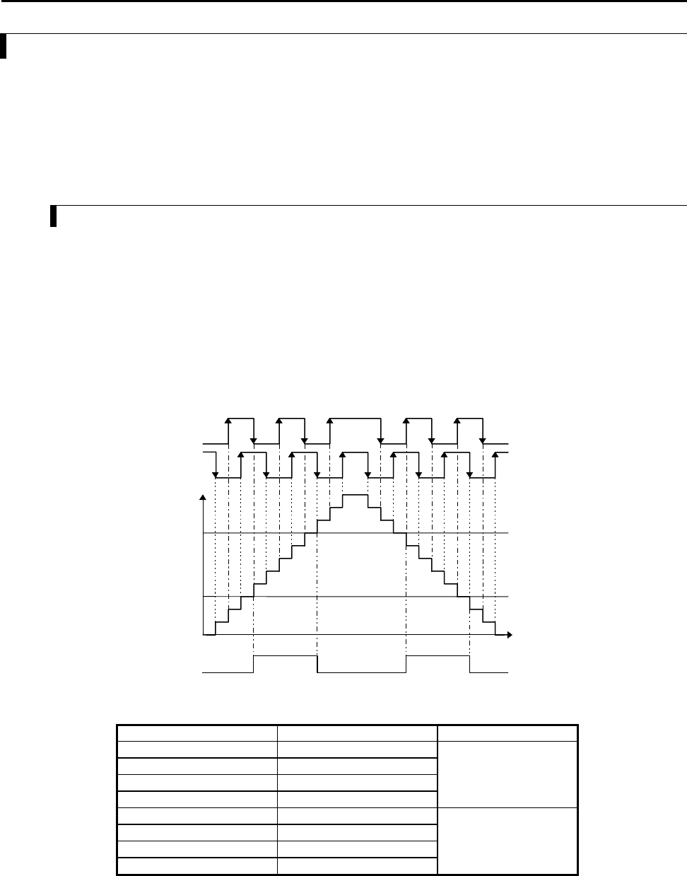
Chapter 8 High-speed counter, PWM / Pulse train output and Analogue I/O
8-10
8.3 High-Speed Counter (Two-Phase Counter)
When operation mode 3 is selected, two-phase counters can be used. Four kinds of phase counting modes are available
for two-phase counters.
The settings of the two-phase counters are stored in the special internal outputs (WRF06F to 72, 76, 7A, and 7E). It is
only possible to perform the settings through the special internal output (WRF071) when the CPU is stopped and the
output is turned off. Once all the input/output settings are completed, the setting of each counter can be changed using the
special internal outputs for individual setting (WRF058), regardless of whether the CPU is operating or stopped. In
addition, the setting can be changed by a program using the FUN instruction (FUN140 to 142, and 146). Refer to the
chapter about the FUN instruction for information about how to use the FUN instruction for setting.
8.3.1 Operation of Two-Phase Counters
The phase counting mode settings are stored in the special internal output (WRF06F). The operation of the counter values
is the same as for a single-phase counter and likewise wrap around from 0000H to FFFFH. In case of an up counter, the
count value becomes 0000H if one more pulse is input while the current count value is FFFFH. In case of a down counter,
the count value becomes FFFFH if one more pulse is input while the current count value is 0000H. Moreover, the preload
input operation, strobe input operation, and executing operation of the current value clear instruction are run in the same
manner as for a single-phase counter. The status of the counter output is stored in the data memory at the timing of the
refresh process. Therefore, it should be noted that the status monitored by peripheral units, etc. and the actual output
status may be different (by a delay of one scan).
(1) Phase counting mode 0
The counter counts up when input 1A is ahead of input 1B, and down when input 1A is lagging behind input 1B.
Figure 8.14 Counting operation of phase counting mode 0
Input 1A Input 1B Operation
1 (High) ↑ (Rising edge) Up count
0 (Low) ↓ (Falling edge)
↓ (Falling edge) 1 (High)
↑ (Rising edge) 0 (Low)
0 (Low) ↑ (Rising edge) Down count
1 (High) ↓ (Falling edge)
↓ (Falling edge) 0 (Low)
↑ (Rising edge) 1 (High)
Coincidence
output
On preset
value
Off preset
value
Count
value
Input 1B
Input 1A
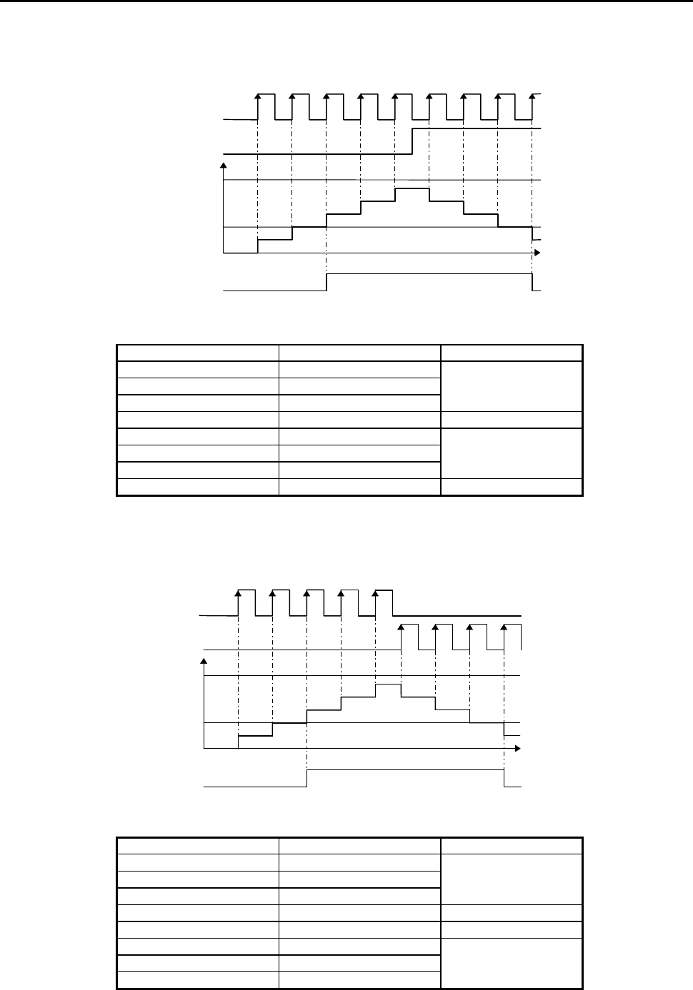
Chapter 8 High-speed counter, PWM / Pulse train output and Analogue I/O
8-11
(2) Phase counting mode 1
In this mode the counter counts at the rising edge of input 1A. At this point, if input 1B is 0 (Low) it counts up, and if
input 1B is 1 (High) it counts down.
Figure 8.15 Counting operation of phase counting mode 1
Input 1A Input 1B Operation
1 (High) ↑ (Rising edge) Do not count
0 (Low) ↓ (Falling edge)
↓ (Falling edge) 1 (High)
↑ (Rising edge) 0 (Low) Up count
0 (Low) ↑ (Rising edge) Do not count
1 (High) ↓ (Falling edge)
↓ (Falling edge) 0 (Low)
↑ (Rising edge) 1 (High) Down count
(3) Phase counting mode 2
In this mode, if input 1B is 0 (Low) at the rising edge of input 1A the counter counts up, and if input 1A is 0 (Low) at the
rising edge of input 1B, the counter counts down.
Figure 8.16 Counting operation of phase counting mode 2
Input 1A Input 1B Operation
1 (High) ↑ (Rising edge) Do not count
0 (Low) ↓ (Falling edge)
↓ (Falling edge) 1 (High)
↑ (Rising edge) 0 (Low) Up count
0 (Low) ↑ (Rising edge) Down count
1 (High) ↓ (Falling edge) Do not count
↓ (Falling edge) 0 (Low)
↑ (Rising edge) 1 (High)
Coincidence
output
On
p
reset
Off
p
reset
Count value
Input 1B
Input 1A
Coincidence
output
On
p
reset
Off
p
reset
Count
value
Input 1B
Input 1A
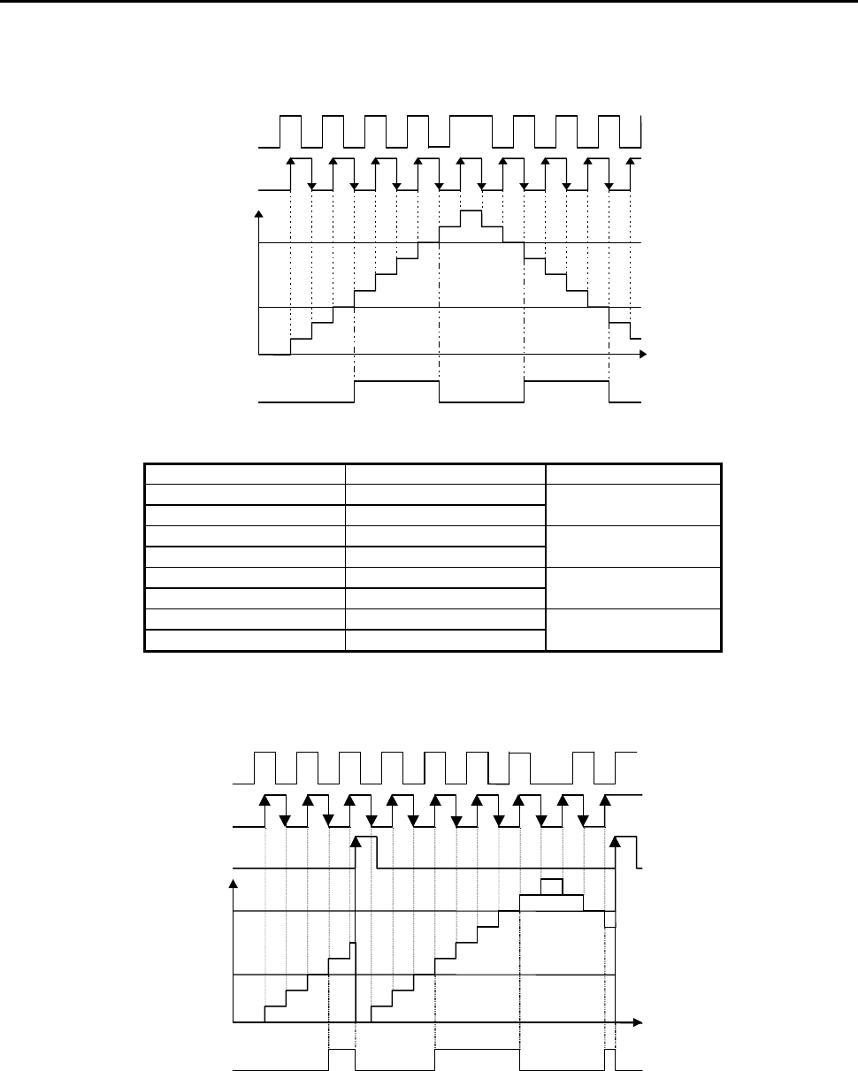
Chapter 8 High-speed counter, PWM / Pulse train output and Analogue I/O
8-12
(4) Phase counting mode 3
In this mode the counter counts at the rising and falling edge of input 1B. It counts up when input 1A is more ahead of
input 1B, and down when input 1A is lagging behind input 1B.
Figure 8.17 Counting operation of phase counting mode 3
Input 1A Input 1B Operation
1 (High) ↑ (Rising edge) Up count
0 (Low) ↓ (Falling edge)
↓ (Falling edge) 1 (High) Do not count
↑ (Rising edge) 0 (Low)
0 (Low) ↑ (Rising edge) Down count
1 (High) ↓ (Falling edge)
↓ (Falling edge) 0 (Low) Do not count
↑ (Rising edge) 1 (High)
(5) Clear input operation (common to all the phase counting modes)
The count value is cleared at the rising edge of input 1Z. As an example, the clear operation of phase counting mode 4 is
shown in Figure 8.18. (The clear operation works identically for all four phase counting modes.)
Figure 8.18 Count value clear operation (phase counting mode 4)
Coincidence
out
p
ut
On
p
reset
Off
p
reset
Count
v
alue
Input 1B
Input 1A
Coincidence
output
On
p
reset
Off
p
reset
Count
value
Input 1Z
Input 1B
Input 1A

Chapter 8 High-speed counter, PWM / Pulse train output and Analogue I/O
8-13
8.3.2 Setting of Two-Phase Counter
The setting of the two-phase counters are stored in the special internal outputs (WRF072 to WRF07E).
(1) Phase counting mode
Set the phase counting mode (0-3) in WRF06E. Please see the chapter 8.3.1 about phase counting mode.
WRF06F: Phase counting mode
Figure 8.19 Special internal output for phase counting mode
(2) Setting the on-preset value
Set the count value (the on-preset value) at which the counter output is turned on (or off). Any value in the range from 0
to FFFFH (0 to 65, 535) can be set. If the on-preset value is set to the same value as the off-preset value, or smaller than
the off-preset value, the counter will not perform any counting (see (4).).
WRF072: On-preset value for two-phase counter
Figure 8.20 Special internal output for setting the on-preset value
(3) Setting the off-preset value
Set the count value (the off-preset value) at which the counter output is turned off (or on). Any value in the range from 0
to FFFFH (0 to 65, 535) can be set. If the off-preset value is set to the same value as the on-preset value, or larger than the
on-preset value, the counter will not perform any counting (see (4).).
WRF076: Off-preset value for two-phase counter
Figure 8.21 Special internal output for setting the off-preset value
(4) Setting the counter preload
When preloading is used, the value to be preloaded should be set for each counter used. Any value in the range from 0 to
FFFFH (0 to 65, 535) can be set.
WRF07A: Preload value for two-phase counter
Figure 8.22 Special internal output for setting the preload value
This special internal output becomes valid immediately after the setting.
(5) Diagnostic error
If the on-preset and off-preset settings contain the same values for one or more counters when the PI/O function setting
flag (R7F5) is turned on, the corresponding bit in the abnormality display special internal output turns on and the
counters with abnormal settings do not perform any counting. (It does not count even if a counter input is entered.) In
addition, the setting abnormal flag (R7F7) turns on.
Bit: 1514131211109876543210
WRF057: a Not used b c d e f g h I
Figure 8.23 Special internal output for input/output function abnormality
Bit Description of abnormality Related terminal
a Total pulse frequency abnormality Y100 to Y103
b Pulse 4 frequency abnormality Y103
c Pulse 3 frequency abnormality Y102
d Pulse 2 frequency abnormality Y101
e Pulse 1 frequency abnormality Y100
f Counter 4 preset value abnormality X6
g Counter 3 preset value abnormality -
h Counter 2 preset value abnormality -
i Two-phase counter 1 preset value abnormality X0 to X3
Chapter 8 High-speed counter, PWM / Pulse train output and Analogue I/O
8-14
(5) Individual counter setting
The on-preset and off-preset values can be changed for each two-phase counter by the special internal output for
individual setting (WRF058) regardless of whether the CPU is operating or stopped. Turn on the corresponding bit in the
following special internal outputs when only the on-preset or the off-preset value should be changed for a two-phase
counter. (To change both settings at the same time, set the “H3” in the corresponding special internal outputs for
individual setting.)
Moreover, when the specified on-preset and off-preset values are the same, the corresponding bit of the error display
special internal output is turned on and operation is performed using the preset value before the setting. (The set value for
the special internal output also returns to the preset value before the setting was made)
15 2 1 0
WRF058: Two-phase
counter Not used a b
Figure 8.24 Special internal output for individual setting of counter setting values
Bit Description
a Off-preset change request
b On-preset change request
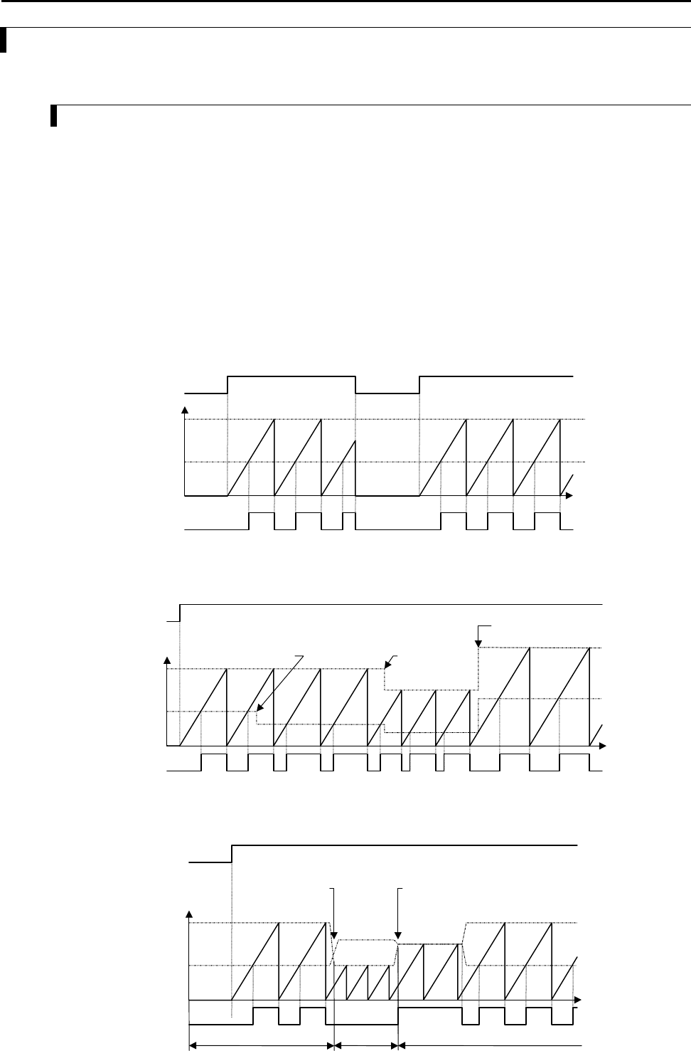
Chapter 8 High-speed counter, PWM / Pulse train output and Analogue I/O
8-15
8.4 PWM Output
A PWM output can be set as an output by setting the operation mode and output terminal. By setting an output to a PWM
output, a pulse with a duty ratio in the range that corresponds to the specified frequency can be output.
8.4.1 Operation of PWM Output
The PWM output settings are stored in the special internal outputs. It is only possible to perform the settings through the
special internal output when the CPU is stopped and the output is turned off. Once all the input/output settings are
completed, the setting of each PWM output can be changed using the special internal outputs for individual setting,
regardless of whether the CPU is operating or stopped. In addition, the settings can be changed by a program using the
FUN instruction (FUN148). See the chapter about the FUN instruction for information about how to use the FUN
instruction for setting.
(1) Basic operation
The special internal outputs R7FC to R7FF are used to control the output. When these special internal outputs are turned
on, a pulse is output at the frequency and the on-duty set in the special internal outputs (WRF072 to 79). When the
special internal output for output control is turned off, the PWM output is also turned off. The special internal outputs
R7FC to R7FF correspond to PWM outputs 1 to 4 (Y100 to Y103); for example, if R7FD is turned on, a pulse train is
output from PWM output 2 (Y101). The on/off status of the PWM outputs is not stored in the data memory. Therefore,
the status of the terminals used for PWM output monitored by peripheral units, etc. may be different from the actual
status of the PWM output terminals.
When a fatal or serious error occurs in the CPU, there will be no output. The output is also stopped if a fatal or serious
error occurs in the CPU during output.
t
R7FC to R7FF
Output pulse
On duty
Frequency
Figure 8.25 Basic operation of PWM output
(2) Operation when setting values are changed
The settings of each PWM output (frequency and on-duty) can be changed by the FUN instruction or the special internal
outputs (WRF072 to 79) regardless of whether the CPU is operating or stopped.
R7FC to R7FF
Output pulse
Change in
frequency
Change in both
frequency and
On duty
Change in On duty
On duty
Frequency
t
Figure 8.26 Operation of PWM output when setting values are changed.
(3) Operation at abnormal settings
The PWM output is not output if the on-duty is set to a value other than the range in use. However, the FUN instruction
does not execute setting change when the setting value is abnormal.
t
R7FC to R7FF
Output pulse
On duty
Normal settings
Abnormal
settings
Normal settin
g
s
Frequency
On-duty setting value:
within the range
On-duty setting value:
exceeding the range
Figure 8.27 Operation of PWM output at abnormal settings
Chapter 8 High-speed counter, PWM / Pulse train output and Analogue I/O
8-16
8.4.2 Setting the PWM Output
The settings of the PWM output operation are stored in the special internal outputs (WRF072 to WRF079).
(1) Setting the PWM output frequency
Set the frequency of output pulse for each PWM output to be used in special internal outputs. The setting values must be
10 to 2000 (HA to H7D0). If the frequency value is set to less than 10 Hz, it is changed to 10 Hz by the system.
It should be noted that the maximum frequency of the PWM output is 2 kHz. Even if a value larger than the maximum
frequency is set, an error flag, etc. will not be output, so be careful not to set a frequency that exceeds 2 kHz.
(Example) If the output frequency is 1 kHz, set “1000” (H3E8) in the special internal outputs.
WRF072: Output frequency for PWM output 1
WRF073: Output frequency for PWM output 2
WRF074: Output frequency for PWM output 3
WRF075: Output frequency for PWM output 4
Figure 8.28 Special internal outputs for setting the PWM output frequency
In case of mode 1, WRF072 and WRF073 are used to set the on-preset value of a counter.
In case of mode 4, WRF072 and WRF075 are used to set the on-preset value of a counter.
(2) Setting the PWM output on-duty value
Set the on-duty value in the corresponding special internal output for each PWM output to be used. The setting values are
0 to 100 (H0 to H64) when the auto correction of on-duty values is not performed. If an on-duty value exceeding this
range is specified, PWM outputs will not be generated. When performing auto correction, the range of on-duty values
that can be set differs depending on the frequency and CPU mode to be set. For more details on the auto correction, see
Section 8.1.5. When a function other than PWM is assigned, this setting is not necessary.
(Example) If the on-duty value is 70 %, set “70” (H46) in the special internal outputs.
WRF076: On-duty value for PWM output 1
WRF077: On-duty value for PWM output 2
WRF078: On-duty value for PWM output 3
WRF079: On-duty value for PWM output 4
Figure 8.29 Special internal outputs for setting PWM output on-duty
In case of mode 1, WRF076 and WRF077 are used to set the off-preset value of a counter.
In case of mode 4, WRF076 and WRF079 are used to set the off-preset value of a counter.
Chapter 8 High-speed counter, PWM / Pulse train output and Analogue I/O
8-17
(3) Effective range of PWM output on-duty values
When correcting on-duty values by setting the value that corresponds to the CPU model in the special internal output
(WRF06B) for setting PWM/pulse output correction, the effective range of the on-duty values differs depending on the
frequency and CPU model to be used. The effective range of the on-duty values is calculated from the following
expressions. For the hardware delay time in the expressions, see Table 6.2.
Caution: There will be a slight error even if correction setting is performed.
On-duty lower limit value (%) = Hardware delay time (µs) x Frequency used (Hz) x 10-4
On-duty upper limit value (%) = 100 - Hardware delay time (µs) x Frequency used (Hz) x 10-4
Table 8.2 Transistor output delay time for each CPU model
CPU model Hardware delay time (TYP) Remark
EH-***DTP 50 µs
EH-***DT 70 µs
EH-***DRP 75 µs
EH-***DRT 25 µs
Example: If the CPU model is EH-***DRP and the PWM output is 2 kHz,
On-duty lower limit value = 50 x 2000 x 10-4 = 10 %
On-duty upper limit value = 100 - (50 x 2000 x 10-4) = 90 %
Thus, the effective range of on-duty values will be 10 % to 90 %.
If correction is not performed (0 is set in WRF06B), on-duty values can be set in the range of 0 to 100 %. However,
caution must be exercised since there will be an error for the period of transistor output delay time between the specified
on-duty and the on-duty that is actually output.
(4) Setting abnormality
When the PI/O function setting flag (R7F5) is turned on, and a value exceeding the effective range of on-duty values is
set for the on-duty setting value of each PWM output (WFR076 to WRF079), PWM outputs will not be generated.
(Example of incorrect setting) PWM output 2 kHz
On-duty setting value (WRF076) - 95
(5) Individual PWM output setting
The frequency and on-duty can be set for each PWM output by the special internal outputs regardless of whether the CPU
is operating or stopped. By setting “H1” in the special internal outputs listed below, it is changed to the frequencies set in
the special internal outputs (WRF072 to WFR075) and the on-duty values set in the special internal outputs (WRF076 to
WFR079). When changing the setting, if any of the on-duty setting values (WRF076 to WRF079) for PWM outputs is set
to a value exceeding the effective range, PWM outputs will not be generated.
15 2 1 0
WRF058: PWM output 1 Not used a
WRF059: PWM output 2 Not used a
WRF05A: PWM output 3 Not used a
WRF05B: PWM output 4 Not used a
Figure 8.30 Special internal outputs for setting individual PWM outputs
Bit Description
a PWM output: individual setting value change request
Chapter 8 High-speed counter, PWM / Pulse train output and Analogue I/O
8-18
8.5 Pulse Train Output
A pulse output can be assigned to an output by setting an output terminal. By setting an output to pulse output, a specified
number of consecutive pulses with a duty ratio of 30 to 70 % can be output. ((To output a pulse having a duty ratio of
50 %, set the value corresponding to the CPU model in the special internal output WRF06B, by referring to Section
8.1.4.) A minimum of 10 Hz to a maximum of 5 kHz can be specified as frequency values. (The maximum frequency of
5 kHz represents the total of all pulse output frequencies.)
8.5.1 Operation of Pulse Output
The settings of the pulse outputs are stored in the special internal outputs. It is only possible to perform the settings
through the special internal output when the CPU is stopped and the output is turned off. Once all the input/output
settings are completed, the setting of each chain output can be changed using the special internal outputs for individual
setting, regardless of whether the CPU is operating or stopped. In addition, by using the FUN instruction, settings can be
changed by a program (FUN150), or pulse outputs with the acceleration/deceleration function can be generated
(FUN151). Refer to the chapter about the FUN instruction for information about how to use the FUN instruction for
setting.
(1) Basic operation
The special internal outputs R7FC to R7FF are used to control the output. When these special internal outputs are turned
on, a pulse train is output at the frequency set in the special internal outputs (WRF072 to 7D) for the set number of pulses.
After the set number of pulses is output, the special internal outputs R7FC to R7FF for output control are turned off by
the system. The special internal outputs R7FC to R7FF correspond to pulse outputs 1 to 4 (Y100 to Y103); for example,
if R7FD is turned on, a pulse is output from pulse output 2 (Y101). If peripheral units, etc. forcefully turn these special
internal outputs off, the pulse output is turned off even if the set number of pulses has not yet been output. The on/off
status of the PWM output is not stored in the data memory. Therefore, the status of the terminals used for pulse output
monitored by peripheral units, etc. may be different from the actual status of the pulse output terminals.
When a fatal or serious error occurs in the CPU, there will be no output. The output is also stopped if a fatal or serious
error occurs to the CPU during output.
In addition, pulses are not output while the backup memory is being written (R7EF=1). Therefore, care should be taken
when handling the pulse output immediately after a program transfer or after a program change while running.
t
Forcefully
turned off
Pulse output
Turned off by
the system
Turned off by
the system
Pulse outputPulse output
Number of output
pulses 2
R7FC to R7FF
Output pulse
Frequency/2
Frequency
Figure 8.31 Basic operation of pulse output
(2) Operation when setting values are changed
The settings of the pulse outputs (frequency and number of output pulses) can be changed by the FUN instruction or the
special internal outputs (WRF072 to 7D) regardless of whether the CPU is operating or stopped. If the settings are made
during the execution of a program in such way that the total frequency of all the pulse outputs exceeds 5 kHz, the
frequency settings will not be changed. Also, the corresponding bit in the abnormality display special internal output is
turned on, and the output will continue to operate at the previously set frequency. (The setting value of the special internal
output also returns to the value set before the abnormal setting was made.)
t
R7FC to R7FF
Output pulse
Frequency/2
Frequency
change (set to
exceed 5 kHz)
In case the frequency becomes 5 kHz or more, the previous setting value is used for operation.
Frequency
change
Frequency change
Frequency
Frequency
change
Figure 8.32 Operation when the pulse output frequency is changed
Chapter 8 High-speed counter, PWM / Pulse train output and Analogue I/O
8-19
To change the number of output pulses, the following operation will be performed:
1] When the number of pulses is to be changed to a value larger than the number of pulses currently being output,
pulses will be output until the number of newly changed pulses is reached, and then the pulse output stops.
2] When the number of pulses is to be changed to a value smaller than the number of pulses currently being output,
the pulse output stops when the current number of pulses is reached.
t
2]
1
]
R7FC to R7FF
Output pulse
Frequency/2
Change of the number
of pulses 6 → 3
Change of the number
of pulses 2 → 4
Frequency
Figure 8.33 Operation for changing the number of pulse output
8.5.2 Setting of Pulse Output
The settings of the pulse outputs are stored in the special internal outputs (WRF072 to WRF07D).
(1) Setting the pulse output frequency
Set the frequency of the output pulse for each pulse output to be used in all of the special internal outputs shown below.
The setting values are 10 to 5000 (HA to H1388). If a value less than 10 Hz is set, it is internally changed to 10 Hz by the
system. When setting the frequencies, make sure that the total value of all pulse output frequencies stays within 5 kHz.
(Example 1) Assuming there is one point of pulse output and the output frequency is 5 kHz:
Setting value = 5000 (H1388)
(Example 2) Assuming there are three points of pulse output and the output frequencies are 1 kHz, 1 kHz, and 3 kHz,
respectively (the settings should be made so that the sum of the output frequencies set for each of the
pulse outputs becomes 5 kHz or less.):
Setting value = 1000 (H3E8)
Setting value = 1000 (H3E8)
Setting value = 3000 (HBB8)
WRF072: Output frequency for pulse output 1
WRF073: Output frequency for pulse output 2
WRF074: Output frequency for pulse output 3
WRF075: Output frequency for pulse output 4
Figure 8.34 Special internal outputs for setting output frequencies
In case of mode 1, WRF072 and WRF073 are used for setting the on-preset value of a counter.
In case of mode 4, WRF072 and WRF075 are used for setting the on-preset value of a counter.
(3) Setting the number of output pulses
Set the number of output pulses for each pulse output used. The setting values are 0 to 65535 (H0 to HFFFF). If the
number of output pulses is set to “0,” no pulses will be output.
WRF07A: Number of output pulses for pulse output 1
WRF07B: Number of output pulses for pulse output 2
WRF07C: Number of output pulses for pulse output 3
WRF07D: Number of output pulses for pulse output 4
Figure 8.35 Special internal outputs for setting number of output pulses
In case of mode 1, WRF07A and WRF07B are used for setting the preload strobe value.
In case of mode 4, WRF07A and WRF07D are used for setting the preload strobe value.
Chapter 8 High-speed counter, PWM / Pulse train output and Analogue I/O
8-20
(4) At setting abnormality
If the sum of the frequencies of the pulse outputs is set to exceed 5 k when the PI/O function setting flag (R7F5) is turned
on, the bit for the total pulse frequency abnormality in the error display special internal output turns on, and none of the
pulse outputs are output. In addition, individual setting of pulse outputs cannot be performed when the bit for the total
pulse frequency abnormality is turned on.
Bit: 1514131211109876543210
WRF057: a Not used b c d e f g h i
Figure 8.36 Special internal output for input/output function abnormality
Bit Description of abnormality Related terminal
a Total pulse frequency abnormality Y100 to Y103
b Pulse 4 frequency abnormality Y103
c Pulse 3 frequency abnormality Y102
d Pulse 2 frequency abnormality Y101
e Pulse 1 frequency abnormality Y100
f Counter 4 preset value abnormality X6
g Counter 3 preset value abnormality X4
h Counter 2 preset value abnormality X2
i Counter 1 preset value abnormality X0
(5) Individual setting of pulse outputs
It is possible to set the frequency and number of output pulses for each pulse output by the special internal outputs for
individual setting, regardless of whether the CPU is operating or stopped. Turn on the corresponding bit in the following
special internal outputs when only the pulse frequency or number of output pulses should be changed.
If the total of frequencies exceeds 5 kHz as a result of performing individual setting of pulse outputs for pulse outputs
that are working normally, the bit for the error display special internal output that corresponds to the changed pulse output
will turn on, and that pulse output will work at the frequency before the setting change. (The value set in the special
internal output also returns to the previous value before the setting was made.)
15 2 1 0
WRF058: Pulse output 1 Not used a b
WRF059: Pulse output 2 Not used a b
WRF05A: Pulse output 3 Not used a b
WRF05B: Pulse output 4 Not used a b
Figure 8.37 Special internal outputs for setting individual pulse outputs
Bit Description
a Number of output pulse change request
b Output pulse frequency change request
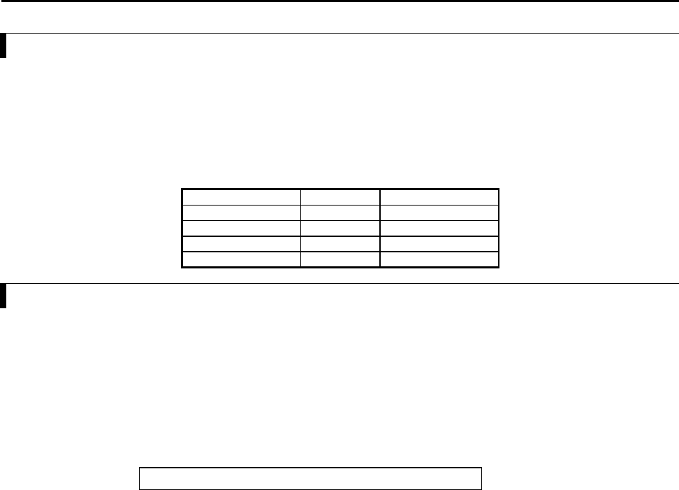
Chapter 8 High-speed counter, PWM / Pulse train output and Analogue I/O
8-21
8.6 Interrupt Input
When either operation mode 0, 1, or 3 is selected, it is possible to assign an interrupt input to X1, X3, X5, and X7 by the
special internal output (WRF07F). (The 10-point type CPU does not have X7.) It is only possible to set them by the
special internal output under the conditions where the CPU is stopped and the output is off.
When an interrupt input is entered, an interrupt process determined by a user program starts up. The INT numbers
corresponding to the interrupt inputs are listed in Table 8.2. See the chapter about the instruction specifications for the
interrupt input processing.
Table 8.3 Interrupt input – correspondence table
Interrupt input Terminal INT No.
Interrupt input 1 X1 INT16
Interrupt input 2 X3 INT17
Interrupt input 3 X5 INT18
Interrupt input 4 X7 INT19
8.7 Digital Filter
The input can set digital filter functions (when assigned normal input functions in X0 to X7 with operation mode 0, 1, or
3, be set to the input too). The sampling number of the digital filter is stored in the special internal output (WRF07F). The
sampling number is set in 0.5ms unit (0 to 40, i.e., 0 to 20ms). When the value 0 is set, there is no filter, and when 41 or
more is set, it is treated as a sampling number of 40 (20ms). This special internal output is stored in the FLASH memory
by turning on the various setting write requests (R7F6). Once the setting is stored in the FLASH memory, it is not
necessary to make the setting again when the power is turned on next time.
The input status is maintained in the buffer for the maximum sampling number. When the input status is read, the status
for the past set number of sampling numbers is looked up, and if there was no change, that status is read. If there were
changes, the status before the change is read.
WRF07F: Input sampling number
Figure 8.38 Special internal output for setting normal input sampling number
The above-mentioned setting is stored immediately upon the completion of the setting. Moreover, it is invalid for inputs
assigned to counter input.
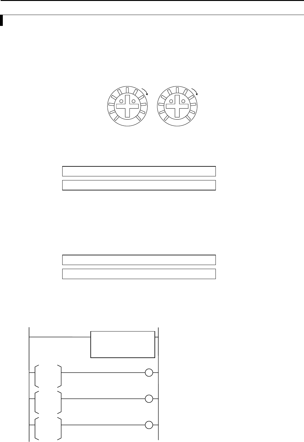
Chapter 8 High-speed counter, PWM / Pulse train output and Analogue I/O
8-22
8.8 Potentiometers
CPUs other than of the 10-point type are equipped with two potentiometers. Through the use of these potentiometers, it
becomes possible to change values in the special internal outputs from the outside using a tool that looks like a
screwdriver. The resolution is 10 bits, so it is possible to adjust the values from 0 to 3FFH (1 to 1,023).
The potentiometers are found under the cover on the left side of the main unit. The value becomes larger when the dial is
turned clockwise and smaller when turned counterclockwise. In addition, this value is always stored in the special
internal output, regardless of whether the CPU is operating or stopped.
HL
VR1
HL
VR2
Figure 8.39 Potentiometers
(1) Values of the potentiometers
The values entered by means of the potentiometers are stored in the following special internal outputs.
WRF03E: Potentiometer 1 input value
WRF03F: Potentiometer 2 input value
Figure 8.40 Potentiometer input value storage special internal output
(2) Setting a filter for the potentiometer
The input values of the potentiometers fluctuate depending on the operating environment of the main unit etc. If the ratio
of fluctuation is to be reduced, a sampling number can be set in the following special internal output. Once the sampling
number is set, the average of the data obtained in the time period determined by the sampling number calculated by
internal processing is set in WRF03E and WRF03F.
The sampling number can be set between 0 and 40 (0 to 28H). If 0 is set, the data without average is stored in WRF03E
and WRF03F. If a value greater than 41 is set, the sampling number is treated as 40.
WRF06C: Potentiometer 1 data sampling number
WRF06D: Potentiometer 2 data sampling number
Figure 8.41 Special internal output for setting input data sampling number
This special internal output is stored in the FLASH memory by turning on various setting write requests (R7F6). Once it
is stored in the memory, it is not necessary to set the value again when the power is turned on for the next time.
(3) Example
The following shows a simple ladder program using the potentiometers:
By turning potentiometer 1, one of flags Y100 to Y102 turns on.
1] Always substitute the value of potentiometer 1 to
WR0.
2] Delete the lower four bits of WR0 (because lower
four bits are more prone to error due to changes in
resistance caused by temperature, etc.)
3] If WR0 is “0,” Y100 is turned on.
4] If WR0 is 1F, Y101 is turned on.
5] If WR0 is 3F, Y102 is turned on.
WR0 = WRF03E
LSR(WR0,4)
Y102
Y101
Y100
WR0
==
0
WR0
==
1F
WR0
==
3F
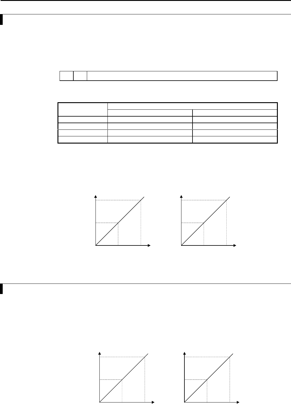
Chapter 8 High-speed counter, PWM / Pulse train output and Analogue I/O
8-23
8.9 Analogue Input
The 23-point type CPU is equipped with two points of analogue input. The input to these two points can be set to voltage
input or current input individually. The setting of current or voltage input is made in the special internal output WRF06E.
This special internal output is stored in the FLASH memory by turning on various setting write requests (R7F6). Once it
is stored in the memory, it is not necessary to set the value again when the power is turned on for the next time.
Bit: 1514131211109876543210
WRF06E: ab Not used
Initial value: 00
Figure 8.42 Special internal output for selecting the analogue type
FunctionWRF06E
Setting value Analogue CH0 (Bit a) Analogue CH1 (Bit b)
C000H Current input Current input
8000H Current input Voltage input
4000H Voltage input Current input
0000H Voltage input Voltage input
Please note that the external wiring is different for voltage input and current input. See the section regarding analogue
system wiring for the details.
Through the above-mentioned settings, the input data of channel 0 is stored in WX 30 and the input data of channel 1 is
stored in WX31. The correspondence between analogue data and digital data is shown in the figure 8.40 (divide 0 to 10 V
and 0 to 20 mA in 0 to 4000). The voltage data is converted to 0.0025 [V] per 1H and the current data is converted to
0.005 [mA] per 1H. Therefore, the value ranges that can be measured from the output channel are 0 to 10.2375 [V] for
voltage data and 0 to 20.475 [mA] for current data, respectively.
1050
7D0H
FA0H
V
(4000)
(2000)
20100
7D0H
FA0H
mA
(4000)
(2000)
Figure 8.43 Correspondence diagrams of digital and analogue input
(Example)
If analogue input channel 0 is set to voltage input and the analogue input channel 1 is set to current input, and 3V and
14mA are applied respectively, 4B0H (1200) is stored in WX30 and AF0H (2800) is stored in WX31.
8.10 Analogue Output
The 23-point type CPU is equipped with one point of analogue output. In analogue output, digital values set at WY40 are
converted to analogue output, and then output. Switching between voltage output/current output is performed by external
wiring; analogue voltage outputs are output when connected to a voltage output terminal, and analogue current output
when connected to a current output terminal.
The correspondence between analogue data and digital data is shown in the figure 8.41 (divide 0 to 10 V and 0 to 20 mA
in 0 to 4000). The voltage data is converted to 0.0025 [V] per 1H and the current data is converted to 0.005 [mA] per 1H.
Therefore, the values that can be output from the output channel are 0 to 10.2375 [V] for voltage data and 0 to 20.475
[mA] for current data, respectively.
10
5
07D0H
(2000)
FA0H
(4000)
V
20
10
07D0H
(2000)
FA0H
(
4000
)
mA
Figure 8.44 Correspondence diagrams of digital and analogue output
(Example)
If 5F0H (1520) is set in WY40, 3.8 V is output from the analogue voltage output terminal. When reconnected to the
analogue current output terminal, 7.6 mA is output. Please note that if connected to both terminals by mistake, the correct
output value will not be output.
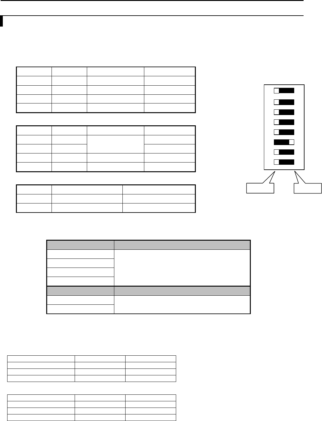
Chapter 8 High-speed counter, PWM / Pulse train output and Analogue I/O
8-24
8.11 Analogue Expansion unit
Analogue expansion module has 4 ch. of analog input and 2 ch. of analog output, which is configured by dip switches.
Range setting
Analogue input range setting (Common for all input channels.)
Sw1 Sw2 Range Remarks
off off 0 - 10V Default setting
off ON 0 - ±10V
ON off 0 - 20mA
ON ON 4 - 20mA
Analogue output range setting (Common for all output channels.)
Sw3 Sw4 Range Remarks
off off Default setting
off ON 0 - 10V
ON off 0 - 20mA
ON ON 4 - 20mA
Conversino mode
Sw6 Conversion mode Remarks
off 4,096 (H0FFF)
ON 4,000 (H0FA0) Default setting
Sw5,7,8 : Set off always.
I/O assignment, data table
I/O assignment = "FUN 0"
WX u00 System area Do not use this area.
WX u01 Ch.1 Input data
WX u02 Ch.2 Input data
WX u03 Ch.3 Input data
WX u04 Ch.4 Input data
Data in lower 12 bits.
Always 0 in higher 4 bits.
0000H - 0FFFH
WY u05 System area Do not use this area.
WY u06 Ch.6 Output data
WY u07 Ch.7 Output data
Data to be written in lower 12 bits.
0000H -0FFFH
u : Unit number (1 - 4)
Example : Unit 1, Input ch.2 → WX102 Unit 4, Output ch.7 → WY407
In/output data table
0 - 10V / 0 - 20mA / 4 - 20mA
Mode 4000 Mode 4096
0V / 0mA / 4mA 0 0
5V / 10mA / 12mA H07D0 (2000) H07FF (2047)
10V / 20mA / 20mA H0FA0 (4000) H0FFF (4095)
-10 - +10V (only for analog input)
Mode 4000 Mode 4096
-10V H0830 (-2000) * H0800 (-2048) *
0V 0 0
+10V H07D0 (2000) H07FF (2047)
* 2's complement
SW1 → 1 O
N
OFF ON
Dip switch
(Default setting)
Caution : Set dip switch while power off.
SW2 → 2
SW3 → 3
SW4 → 4
SW5 → 5
SW6 → 6
SW7 → 7
SW8 → 8
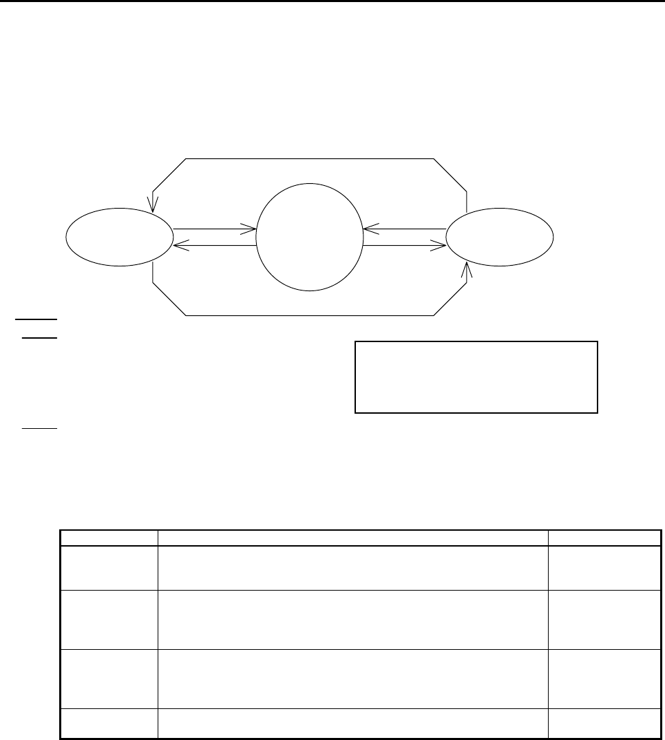
Chapter 9 PLC Operation
9-1
Chapter 9 PLC Operation
The operating status and stop status of the MICRO-EH can be switched through various types of operations. This feature
is shown in Figure 9.1.
Stop status
Switch “STOP” or
operation definition
input “OFF”
Switch “RUN” and
operation definition
input “ON”
Switch “STOP”
Switch “RUN”
Designate operation definition input
Cancel operation definition input
Stop status Operating status
Caution
The MICRO-EH cannot handle a REMOTE
specification. A 10-point type CPU becomes
the RUN mode when the RUN input is On.
Figure 9.1 Transitional diagram between operating and stop statuses
The MICRO-EH can be operated or stopped under the conditions as shown in Figure 9.1. If an error is detected during
operation or stop, output is shut off, an error is displayed and the MICRO-EH stops. There are fatal error, serious error,
minor error and warning. The operating status for each error is listed in Table 9.1.
Table 9.1 Description of each error and operating status
Classification Description Run/Stop
Fatal error This indicates there is a fatal and unrecoverable error, such as a power
supply problem, microcomputer error, system ROM error, system RAM
error and system path error.
Stops
Serious error This indicates there is an error such as data memory problem, system
program problem, user memory problem, user memory size error,
syntax/assembler error, etc., which may cause a malfunction if operation is
continued.
Stops
Minor error These are errors such as I/O information verify error, remote problem,
congestion error, excessively assigned I/O points, etc. The operation may be
continued when a continue operation is set by the user programs.
Stops
(continued operation
is possible if
specified)
Warning These are problems such as a transfer error, backup memory write problem,
etc. where it is possible to continue the operation.
Operation continues
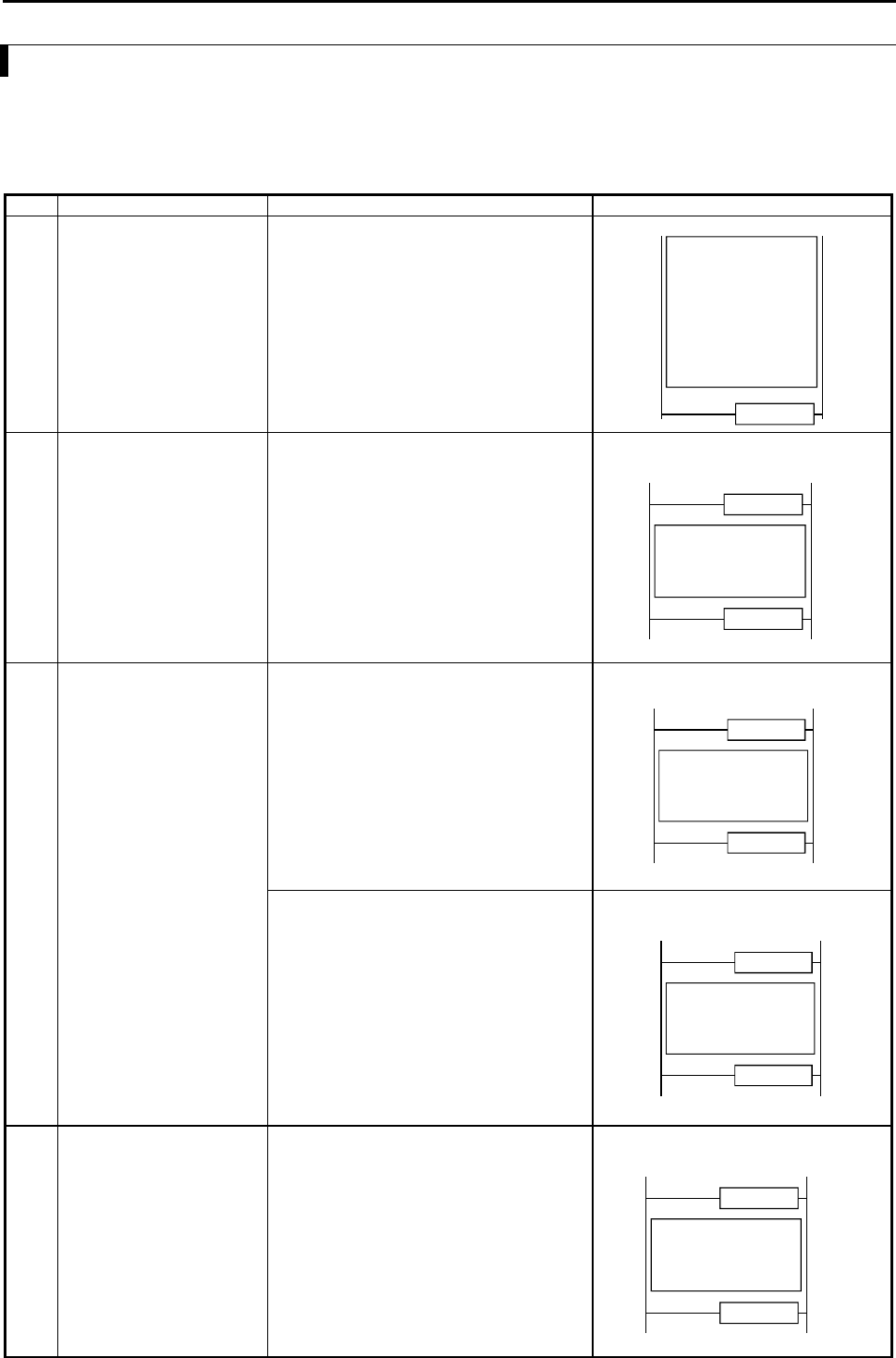
Chapter 9 PLC Operation
9-2
9.1 RUN Start
When the MICRO-EH switches to the operating state, the user program is executed in sequence from the beginning. The
user programs consist of a normal scan program and periodical scan program. In addition to these programs, there is a
subroutine area defined as a subroutine.
Table 9.2 Program classification
No. Program classification Description Expression
1 Normal scan program This is the program that is normally executed.
When the program has been executed to the
END instruction, execution starts again from
the beginning.
Congestion error is monitored according to the
congestion check time set by the user. It is
monitored from the beginning of the program
to the END instruction.
When it is specified to continue during
congestion (R7C0), the operation continues
even if a congestion error occurs. END
Normal scan
program
2 Periodical scan program This program is executed periodically at
intervals of 10 ms, 20 ms, or 40 ms.
INT0: Every 10 ms
INT1: Every 20 ms
INT2: Every 40 ms
Each execution cycle time becomes a
congestion error monitoring time.
When it is specified to continue during
congestion (R7C1), the periodical scan
program is suspended during operation.
Described in the area after the END
instruction.
RTI
INTn
n = 0, 1, 2
Periodic scan
program
3 Interrupt scan program When there is an input to the input terminal
assigned to the interrupt input, the interrupt
program (INT16 to INT19) corresponding to
that input starts up.
If another interrupt caused by the same factor
occurs during the execution of the interrupt
program, a congestion error occurs. When the
operation continuation at a congestion error
(R7C2) is specified, the same interrupt scan
program is run from the beginning again.
Described in the area after the END
instruction
If the counter value exceeds the preset value, a
corresponding interrupt program (INT20 to
INT27) starts up according to the counter
number.
Described in the area after the END
instruction
4 Subroutine This is a program called by the CALL
instruction.
Described in the area after the END
instruction
RTS
SBn
n = 0 to 99
Subroutine
program
RTI
INTn
n = 16 to 19
Interrupt scan
program
RTI
INTn
n = 20 to 27
Interrupt scan
program
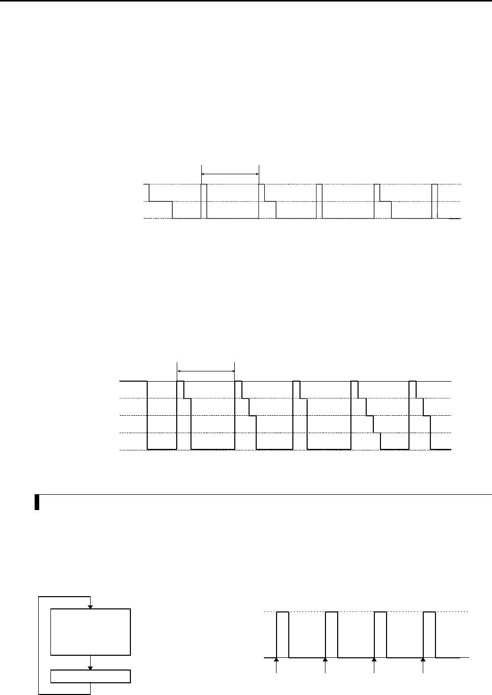
Chapter 9 PLC Operation
9-3
Each program is executed in the order of the priority shown in Figure 9.2. Each program is executed while monitoring
the execution time of each program area. If the monitored time exceeds the specified time, this causes a congestion error
and operation stops. When continued operation has been specified, operation continues.
The timing for scan execution is shown in Figure 9.2. System processing is performed at set periods (every 5 ms),
followed by communication system processing. *1 The maximum execution time of communication system processing
equals the duration of time until the next periodical system processing is started. If the communication system processing
ends before the maximum execution time is up, execution of scan processing is started upon completion of the
communication system processing. When the next periodical processing is executed, scanning is performed until the next
periodical processing is executed.
*1: Communication system processing is executed every 10 ms.
*2: The execution of scan processing starts after the communication system processing is completed.
5 ms
Periodic system processing
Communication system processing
Scan processing
1] 2] 1] 2]
Figure 9.2 Relationship between system processing and scanning
Note: Processing 1 takes extremely short period of time as compared with Processing 2. Therefore, in the following
diagram Processing 1 is omitted in order to avoid complexity.
As shown in Figure 9.3, scan processing is done while periodical scanning is performed. Periodical scanning is
processed at the point when switching to normal scan. Periodical scans are performed at intervals of every 10 ms, 20 ms,
or 40 ms. In terms of priority of execution, 10 ms scans have the highest priority. Use the refresh instruction when you
wish to perform data processing for the external I/O (X, Y) in the periodical scan.
Update processing of timer progress value is performed as a part of system processing.
10 ms
System processing
Periodic scan (10 ms)
Periodic scan (20 ms)
Periodic scan (40 ms)
Normal scan
Figure 9.3 Scan execution timing
9.1.1 Normal Scan
(1) Definition and operation
The normal scan refers to the calculations and execution of the ladder/instruction language program (excluding interrupt
programs) until the END scan processing caused by the END instruction or the execution of programs written in Pro-H.
The time required for one scan, from the beginning of a normal scan program to the END scan processing, is called the
normal scan time.
Figure 9.4 Operation of normal scan
Ladder or instruction
language program
END scan processing
(system self-diagnosis)
END scan processing
Ladder or instruction
language program
(excluding interrupt
program)
END
instruction
END
instruction
END
instruction
END
instruction
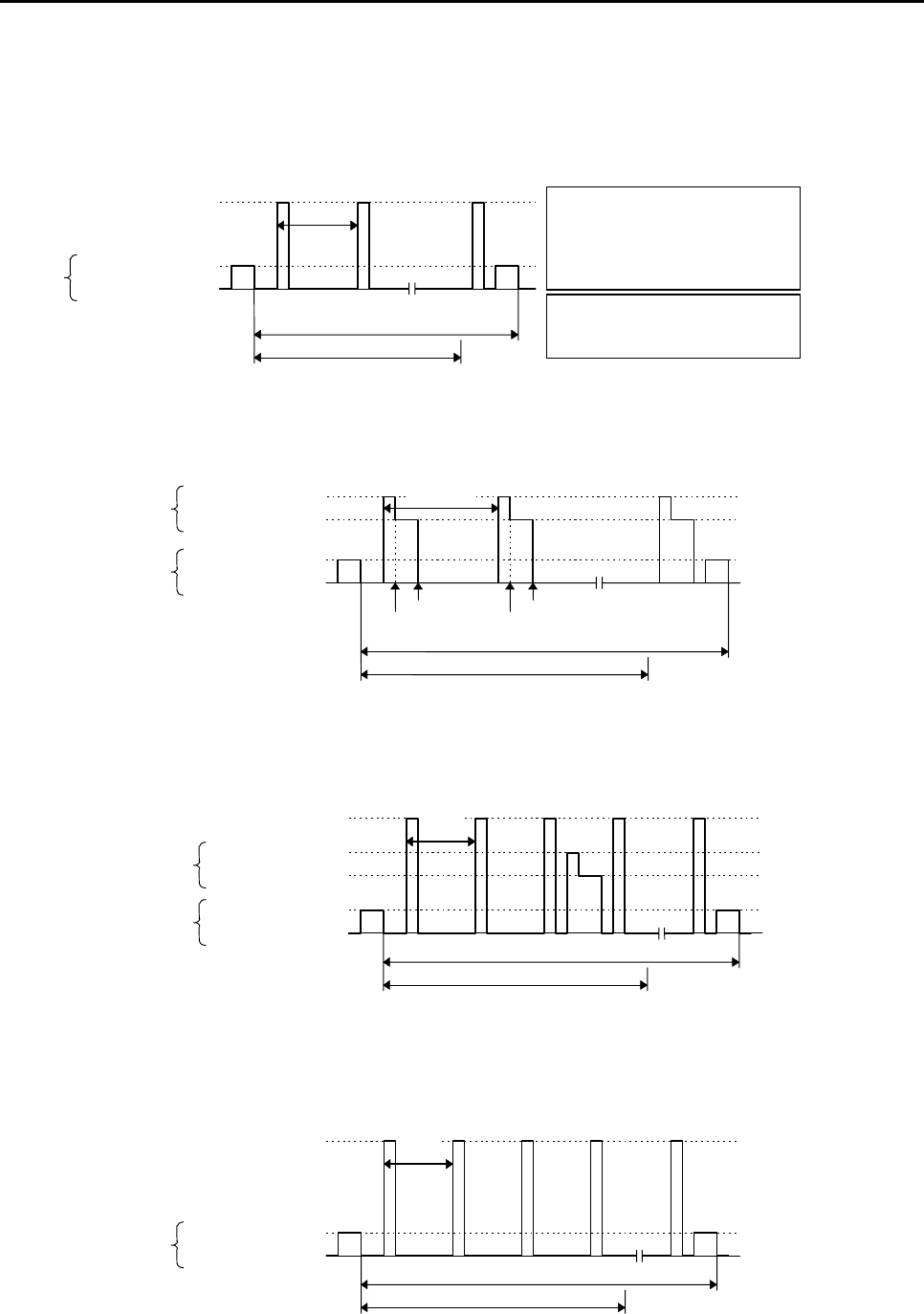
Chapter 9 PLC Operation
9-4
(2) Causes of congestion errors at normal scan
Congestion errors may occur at normal scan because of the following three possible reasons. In particular when using a
periodical scan program and an interrupt scan program together, care must be taken to create the program in such a way
that the total scan time does not exceed the congestion check time.
(a) When only a normal scan program is used
The scan time exceeded the congestion check time because the time required for one scan was too long.
Figure 9.5 Congestion error at normal scan (a)
(b) When both a normal scan program and a periodical scan program are used
The congestion check time was exceeded because the periodical scan program was executed and the normal scan
time became longer.
Figure 9.6 Congestion error at normal scan (b)
(c) When both a normal scan program and an interrupt scan program are used
The congestion check time was exceeded because the interrupt scan program was executed due to an interrupt
input and the normal scan time became longer.
Figure 9.7 Congestion error at normal scan (c)
(3) Continuation of operation after a congestion error occurred
When the special internal output bit R7C0, which specifies whether the operation should continue after a congestion
error occurred, is turned on, the normal scan executes the scan until the end regardless of the congestion check time, and
after executing the END scan processing, executes the normal scan from the beginning again.
Figure 9.8 Operation when operation continuation at congestion error is set
However, note that this setting does not stop the execution of the scan when a congestion error occurred even when an
infinite loop is formed within the normal scan by the JMP instruction.
10 ms
The periodical system interrupt
is executed by interrupts at every
10 ms regardless of whether or
not there is a periodical scan or
interrupt scan.
The congestion check time can
be set to 20 ms to 2550 ms using
peripheral devices by the users.
Normal
scan
END scan processing
Program execution
Periodical system processing
Congestion check time
Normal scan time (normal scan only)
RTI
INT0
10 ms
RTI
INT0
N
ormal
scan
END scan processing
Program execution
Periodical system
processing
Periodical program
Congestion check time
Sc
an tim
e
Periodical
scan
10 ms
N
ormal
scan
END scan processing
Program execution
Periodical s
y
stem
p
rocessin
g
Congestion check time
Sc
an tim
e
Interrupt analysis
processing
Pro
g
ram execution
I
nterrupt
scan
10 ms
N
ormal
scan
END scan processing
Program execution
Periodical system processing
Congestion check time
Scan time
Chapter 9 PLC Operation
9-5
9.1.2 Periodical Scan
(1) Definition and operation
This scan executes interrupt programs (periodical scan programs) while the CPU is operating with a fixed cycle time (10
ms, 20 ms, or 40 ms) specified by the users.
Enter the periodical scan program to be executed between instructions INT0 and RT1 if it should be started up with a 10
ms cycle time, and between INT1 and RT1 if it should be started up with a 20 ms cycle time.
The periodical system processing is executed every 10 ms regardless of whether or not there is a periodical scan program.
Figure 9.9 Operation of periodical scan (in case of INT1)
(2) Causes of congestion errors at periodical scan
If there are periodical scans at every 10 ms as well as scans at every 20 ms or 40 ms, a congestion error occurs and the
scan is stopped if the periodical scan at 10 ms is started up again before all the periodical scans are completed (i.e., the
periodical system processing at INT0 to INT2 does not end within 10 ms).
Figure 9.10 Congestion error at periodical scan (10 ms)
Similarly, when executing with a periodical scan at every 20 ms or with a combination of periodical scans at every 20 ms
and 40 ms, a congestion error occurs if the periodical scan at 20 ms is started up again before all the periodical scans are
completed (i.e., the periodical system processing at INT1 to INT2 does not end within 20 ms). Finally, when using a
periodical scan at every 40 ms, a congestion error occurs if the periodical scan at 40 ms is started up again before all the
periodical scans are completed (i.e., the periodical system processing at INT2 does not end within 40 ms).
RTI
INT1
10 ms
20 ms
RTI
INT1 INT1
Normal scan
Scan every 40 ms
Periodical program
Scan every 20 ms
Periodical program
Scan every 10 ms
Periodical program
Periodical system
processing
Periodical scan
Program execution
Periodical scan
Normal scan
Periodical system processing
(including interrupt analysis
processing)
Interrupt Interrupt Interrupt
INT0
10 ms 10 ms
INT1
INT0
RTI
10 ms
INT2
INT1
INT0
RTIRTI
END scan processing
Normal scan program
Stop
Periodical scan
N
ormal
scan
(Example 3)
Before the periodical scan program
at every 40 ms ends, the periodical
interrupt at 10 ms is started up again.
(Example 2)
Before the periodical scan program at
every 20 ms ends, the periodical
interrupt at 10 ms is started up again.
(Example 1)
Before the periodical scan program at
every 10 ms ends, the periodical
interrupt at 10 ms is started up again.
Scan every 10 ms
Periodical program
Scan every 20 ms
Periodical program
Scan every 40 ms
Periodical program
Periodical system processing
Stop
Stop
Chapter 9 PLC Operation
9-6
(3) Continuation of operation after a congestion error
If a congestion error occurs when the special internal output bit R7C1, which specifies whether the operation should
continue after a congestion error, is turned on, the execution of the periodical scan is stopped and the periodical scan is
executed from the beginning again. If the operation continuation specification for the normal scan is Off when this
happens, the scan stops as a congestion error at a normal scan. If the operation continuation specification for the normal
scan is On, only the periodical scan continues to be executed in the event of a periodical congestion error. Care must be
taken because the normal scan is not executed under this condition.
Figure 9.11 Operation when operation continuation at congestion error is set
9.1.3 Interrupt Scan
(1) Definition and operation
If there is an input to an input terminal assigned to an interrupt input, or there is an input to an input terminal assigned to
a counter input and the current counter value exceeds the preset value while the CPU is operating, interrupt programs
(interrupt scan) corresponding to them are started up. An interrupt scan caused by an interrupt input executes interrupt
programs from INT16 to19 to RTI instructions. An interrupt scan due to a corresponding interrupt caused by the counter
current value executes the interrupt programs from INT20 to INT27 to RTI instruction.
If an interrupt caused by another factor is input during the execution of an interrupt scan, the next interrupt scan is
started up at the point when the interrupt scan being executed is completed. Also, if two or more interrupts are input
during the execution of an interrupt scan, the interrupt scans are started up in order from the smallest INT number at the
point when the interrupt scan being executed is completed.
Figure 9.12 Operation of interrupt scan
(2) Causes of congestion errors at interrupt scan
An interrupt scan congestion error occurs during the interrupt scan processing when an interrupt of the same number is
entered again.
In addition, a normal scan congestion error occurs if interrupt inputs are frequently entered because a normal scan cannot
be executed.
Figure 9.13 Operation of interrupt scan
INT0
10 ms
INT0
END scan processing
Normal scan program
Periodical
scan
Normal
scan
Scan every 10 ms
Periodical program
Scan every 20 ms
Periodical program
Scan every 40 ms
Periodical program
Periodical system processing
R7C0 On/R7C1 On: Continue
R7C0 Off/R7C1 On: Stop
Congestion check time
Periodical interrupt Periodical interrupt (10 ms
periodical interrupt restarts)
RTI
INT20
INT17
INT16
INT17
INT16INT20 INT16
INT20
INT17
RTI
RTI
RTI
RTI
RTI
10 ms
Normal scan
Periodical system
processing
Interrupt analysis processing
Interrupt scanNormal scan
Interrupt analysis
p
rocessin
g
Execution of
interrupt program
10 ms
N
ormal
scan
END scan processing
Program execution
Periodical system processing
Interrupt analysis
processing
Interrupt scan Stop
I
nterrupt
scan
The interrupt contact of INT16 is turned
on during the execution of the INT16
program.
Interru
p
t contact on
(
INT16
)
Interrupt contact on (INT16)
Chapter 9 PLC Operation
9-7
(3) Continuation of operation after a congestion error occurred
If an interrupt scan congestion error occurs when the special internal output bit R7C2, which specifies whether the
operation should continue after a congestion error, is turned on, the interrupt scan is started anew and the scan is
executed from the beginning again. Therefore, if the operation continuation specification of the normal scan is Off under
the conditions where interrupt inputs are frequently entered from the external source, this scan is stopped as a normal
scan congestion error. If the operation continuation specification of the normal scan is On, only interrupt scans are
continuously executed depending on the condition of the interrupt congestion error. Care must be taken because normal
scans are not executed under this condition.
Figure 9.14 Operation when operation continuation at congestion error is set
INT16
INT16
INT16
Normal
scan
END scan processing
Program execution
Periodical system processing
Interrupt analysis
processing
Interrupt scan
Congestion check time
Interrupt contact on
Interrupt
scan
Interrupt contact on
Interrupt contact on
R7C0 On/R7C2 On: Continue
R7C0 Off/R7C2 On: Stop
Chapter 9 PLC Operation
9-8
9.1.4 Relationship of Each Scan Type
When three types of scan occur at the same time, scan is executed in the order of periodical scan, then interrupt scan, and
then normal scan.
Figure 9.15 Relational diagram of scan operation
Table 9.3 List of interrupt label
Interrupt label Cause of startup Interrupt label Cause of startup
INT0 Interrupt every 10 ms INT20 Counter 1 on-preset match
INT1 Interrupt every 20 ms INT21 Counter 1 off-preset match
INT2 Interrupt every 40 ms INT22 Counter 2 on-preset match
INT16 Interrupt of interrupt input 1 INT23 Counter 2 off-preset match
INT17 Interrupt of interrupt input 2 INT24 Counter 3 on-preset match
INT18 Interrupt of interrupt input 3 INT25 Counter 3 off-preset match
INT19 Interrupt of interrupt input 4 INT26 Counter 4 on-preset match
INT27 Counter 4 off-preset match
Low High
Execution priority
Interrupt scan Periodical scanNormal scan
Normal
scan
Ladder program
END scan
Processing
Normal scan
Interrupt scan
10 ms10 ms10 ms10 ms
Periodical scan
Periodical system processing
INT16
INT17
INT18
:
:
INT27
10 ms periodical
program
20 ms periodical
program
40 ms periodical
program
Interrupt analysis
processing
Interrupt program
Interrupt
scan
Periodical
scan
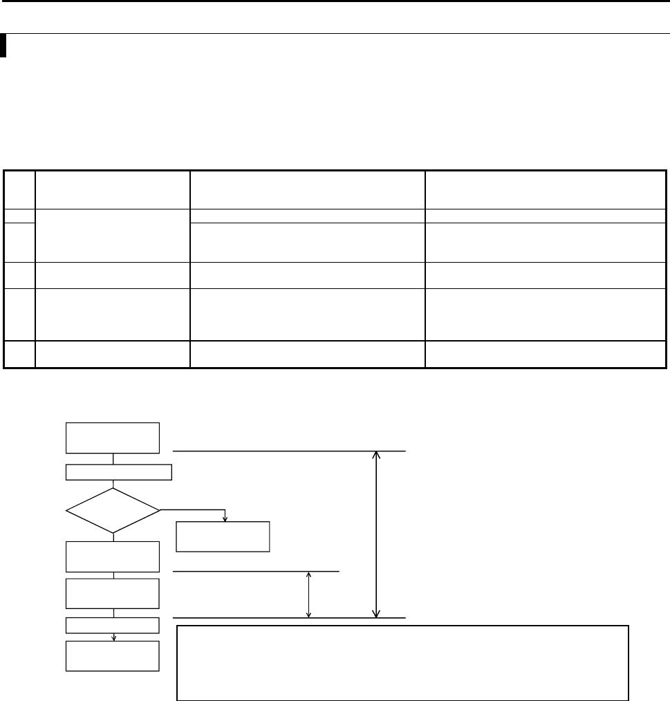
Chapter 9 PLC Operation
9-9
9.2 Online Change in RUN
The user programs can be modified during operation while retaining the output status as is. This is called the “program
change while running” function. To modify the user programs, special programming software or programmer is required.
Refer to the individual manuals on the operation.
Program change while running cannot be executed in the following situations. Perform this operation after satisfying the
conditions.
Table 9.4 Conditions for performing program change while running
No
Conditions under which
program change while
running cannot be performed
Specific situation How to satisfy the conditions
1 When READ-occupying Other programming device is connected. Change other programming devices to off-line.
2 When a personal computer or panel, etc. is
connected and monitoring is being executed.
Change the personal computer or panel to off-line.
(When monitoring, it is convenient to use the
occupancy unnecessary task code.)
3 END instruction is not executed. A program that runs in an infinite loop is being
executed.
Correct the program so that it does not run in an
infinite loop.
4 Attempted to modify a program
that includes control
instructions.
Performing program change while running for a
circuit containing a control instruction may cause
operation to stop depending on the type of the
program modification error.
An explanation of how to perform program change
while running for a circuit that contains a control
instruction is given in the programming software
manual.
5 A password has been set. A program protected by a password cannot be
modified.
Execute after having the system administrator
remove the password.
(When the CPU is stopped, the update is executed without displaying a message confirming program change while
running.)
The MICRO-EH operation when the user program is changed in RUN is shown below.
Note
The special internal output R7EF turns on during the transfer to the FLASH memory.
If the power supply to the CPU is turned off during transferring to the FLASH memory, the programs may be
destroyed. Before the power supply to the CPU is turned off it should be confirmed that R7EF is off, or it should
not be turned off until after approximately two minutes upon the completion of program transfer.
(If the pulse is being output, turn off the power supply approximately two minutes after the pulse output stops.)
OK
NG
Scan resumes
Program change
while running
Scanning stops
at END scan
Program modification
Transfer to
FLASH memory
Assemble
check
Transfer to operation
execution memory
Error stop
(output shuts off)
HALT time
Program change
while running
including control
command
Displays that program change
while running is being performed
(programming device)
Figure 9.16 Internal processing for program change while running
Transfer to the FLASH memory
Unlike the conventional H/EH series, the MICRO-EH transfers its user program to the FLASH memory, the backup
memory, during the idle time of the CPU processing. Because of this, when the transfer to the operation execution
memory is completed, the peripheral unit displays that the transfer is complete. However, the transfer to the FLASH
memory is not completed at this stage. If the power supply to the CPU (especially CPUs without battery or CPUs whose
data maintenance guarantee time is over) is turned off at this status, a user memory error (31H) occurs when the power
supply to the main unit is turned back on. Therefore, it should be confirmed that the FLASH memory writing flag
(R7EF) is off before the power supply to the main unit is turned off, or it should not be turned off until after
approximately two minutes upon the completion of program transfer. (During pulse output, programs are not transferred
to the FLASH memory until the pulse output is stopped. If the pulse is being output, turn off the power supply
approximately two minutes after the pulse output stops.)
CPU HALT time
When performing program change while running, the program to be written to the CPU is checked if there are no errors,
then the CPU is halted temporarily (RUN → HALT).
The program of the modified area is written to the CPU while it is halted, and the CPU is set to operate (HALT → RUN)
again.
At this time, the following equation shows the approximate time the CPU is halted (it is not necessarily the maximum value).
HALT time (ms) = 45 × Program capacity (k steps) + 20
An example of a calculation of the HALT time for the MICRO-EH using the above equation is 155 ms.
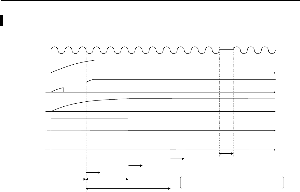
Chapter 9 PLC Operation
9-10
9.3 Instantaneous Power Failure
The following shows operation when the power supply to the MICRO-EH shuts off.
24 V DC
ON
OFF
1.2 s
1.0 s
RUN
Power on
2 s
Reset processing
STOP status
RUN status
(Starts operation)
A
C power supply
Internal 5 V DC
Internal reset
MICRO-EH operation
Instantaneous power failure
When power supply of 100 V AC is used:
operation continues for 10 ms or less
When power supply of 200 V AC is used:
operation continues for 20 ms or less
(1) Powering on
The MICRO-EH starts operations after a maximum of 3.5 seconds have elapsed after power-up. If the power for
input module is not completely started when the operation is commenced, the input that is supposed to be on will
be received as Off and operation proceeds, so make sure that the power for I/O module is completely turned on
before operation is commenced.
Note: When extending with a CPU larger than 14-point type, turn on the power supply for both base and
extension sides at the same time.
(2) Instantaneous power failure actions
(a) When 100 VAC is supplied
Operation is continued during instantaneous power failures that last less than 10 ms.
(b) When 200 VAC is supplied
Operation is continued during instantaneous power failure that last less than 20 ms.
Note: Make arrangement so that the power for input module is supplied while the CPU continues its operation. If
the power is not supplied, the CPU will perform operation assuming the input data as Off. Exercise caution
especially when performing operation that changes the contents of the power failure memory using input
signals, since the contents of the power failure memory may have been altered unintentionally due to an
instantaneous power failure.

Chapter 9 PLC Operation
9-11
9.4 Operation Parameter
The settings of “parameters,” which are required to perform tasks such as creating programs, transferring programs to the
CPU, are performed. The setting contents are explained below.
Item Function Description When to use the function
1 Password {Register a password to a program in the four-digit
hexadecimal format. The program with a password will
not allow program operation nor changes unless the
correct password is entered, so please exercise caution.
Note: The user will not be able to reset the password when
it is forgotten, so exercise extreme caution when accessing
a password.
Password is not set at the time of shipment.
Use to protect the confidentiality
of the programs.
2CPU type {Set the CPU name used to perform programming.
Set the CPU type to “H-302” for MICRO-EH.
Always perform these settings
when programming.
3 Memory assignment {Set the memory capacity.
Set the memory type to “RAM-04H” for MICRO-EH.
Always perform these settings
when programming.
The number of program steps
that can be input is 3072.
4 Operating parameters {Operation control
Perform these settings when controlling the running and
stopping of the operation using a specific I/O. If this is not
set, operation will start automatically by setting the RUN
switch (or the RUN terminal) to “RUN.”
{Congestion check time
Set this when you wish to stop the CPU operation when
the set maximum processing time for a normal scan is
exceeded. When this setting is not made, this is
automatically set to initial value 100 ms.
{Operating mode at problem occurrence
Set this when you wish to continue the CPU operation
when the error generated by the CPU is minor.
Set according to the user's
operation purposes.
5 I/O assignment {This sets the I/O assignment information of the CPU.
It is convenient to use the MICRO-EH's I/O assignment
copy function.
Always perform these settings
when programming.
6 Program name Set the program name using a maximum of 16 alphanumeric
characters. The set program names can be written into the CPU
along with the program, which will facilitate the program
verification and management.
Set this to facilitate program
verification and management.
7 Power failure
memory*
This sets the range in which the data in a specified area in the
CPU is to be stored upon CPU power off or when commencing
RUN. Settings for R, WR, WM, TD, DIF, DFN are possible.
Set this when there is data you
wish to maintain when operation
is stopped.
The special internal output data
is unconditionally saved for
power failure by the I/O number.
*: 10-point type CPU does not have the power failure memory function. Even though it is possible to set a power
failure memory area from a peripheral unit, the values that are stored here will not be persistent; do not set this
function.
Moreover, 14-point type CPU can maintain power failure memory only up to 72 hours. Note that non-persistent
values will be stored if the power supply to the main unit is not turned on after these hours have passed. 23- and 28-
point CPUs without a battery can maintain power failure memory for only up to 30 minutes. The data can be retained
for approximately two months by installing a battery.

Chapter 9 PLC Operation
9-12
9.5 Test Operation
(1) Verification of interlock
Verify performance of the interlock in case of unexpected incidents.
Create ladders such as an emergency stop circuit, protective circuit and interlock circuit outside the program
controller. For the relay output module, however, do not control the relay drive power supply to interlock with the
external loads.
(2) Operation without load
Before actually operating the loads in the system, test the program only and verify its operation.
Always perform this if there may damage the other party's equipment due to unexpected operation caused by
program errors or other problems.
(3) Operation using actual loads
Supply power to the external input and external output to verify the actions.
9.6 Forced Set/Reset
It is possible to forcefully set/reset data to specified I/O points using peripheral units, regardless of whether the CPU is
operating or stopped. Refer to the manuals for the peripheral units for how to set/reset forcefully.
Please note that for the special internal outputs related to operation modes, forcefully setting/resetting only the
corresponding special internal output does not enforce the change in the operation mode. For example, when the
frequency of a pulse output should be changed, the frequency will not be changed by just setting the desirable frequency
in WRF072, the special internal output for setting pulse frequency. See Chapter 8, where the setting of the PI/O function
is explained in detail.
9.7 Forced Output
It is possible to use peripheral units to specify single outputs for forced output while the CPU is stopped. Refer to the
manuals for the peripheral units for how to output forcefully.
Table 9.5 lists the differences between the forced set/reset and forced output.
Table 9.5 Differences between forced set/reset and forced output
Forced set/reset Forced output
I/O types that can be used X,Y,M,R,TD,SS,CU, CT,WX,WY,
WM,WR, TC,DX,DY,DM,DR
Y,WY,DY
CPU status in which the
function can be used
During RUN and being stopped Being stopped
Function Changes the data in the area that stores
the CPU calculation result to a
specified value.
Turns only one specified external
output (one point or one data) on/off
while the CPU is being stopped.
All other outputs are turned off.
Application For checking when setting/changing
power failure memory area data at
troubles.
For checking the wiring for external
output.
Note:
1] The actual external output status and the external output information stored internally in the CPU may be different
when the CPU is stopped. At this point, if a forced set/reset is performed to the external output, the external output
information stored internally in the CPU is output from other external output. Thus, the forced output function can
be used in order to check the wiring for the external output.
2] Only I/O points assigned by the I/O assignment written in the CPU can be set for external input and external output
I/O numbers.
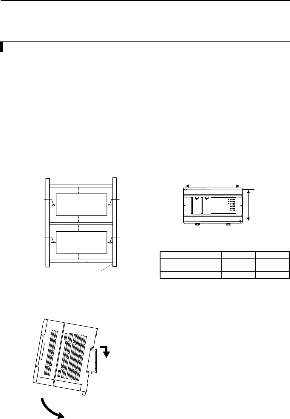
Chapter 10 PLC Installation, Mounting, Wiring
10-1
Chapter 10 PLC Installation, Mounting, Wiring
10.1 Installation
(1) Installation location and environment
(a) When installing the MICRO-EH, use the unit under the environment within the general specification.
(b) Mount the PLC onto a metal plate.
(c) Install the PLC in a suitable enclosure such as a cabinet that opens with a key, tool, etc.
(2) Installing the unit
(a) Precautions when installing the unit
1] When installing the base unit, fix it securely with screws in 2 places (M4, length 20 mm or more) or DIN
rail.
2] To use the unit within the ambient temperature range,
a) Allow ample space for air circulation. (50 mm or more at top and bottom, 10 mm or more to the left
and right)
b) Avoid installing the unit directly above equipment that generates significant heat (heater, transformer,
large-capacity resistance, etc.)
c) When the ambient temperature reaches more than 55 °C, install a fan or cooler to lower the
temperature to below 55 °C.
3] Avoid mounting inside a panel where high-voltage equipment is installed.
4] Install 200 mm or more away from high-voltage lines or power lines.
5] Avoid upside down, vertical or horizontal mounting.
L2
L1
Figure 10.2 External dimensions
Dimensional table
Unit L1 L2
10-point 65 70
14-point (basic, exp.) 85 80
23, 28-point (basic, exp.) 140 80
Unit: mm
(b) Mounting to a DIN rail
Attaching to a DIN rail
1] Hook the claw (top side) attached to the back of
the unit to the DIN rail.
2] Press the unit into the DIN rail until it clicks.
Note: After installation, check to make sure the base
unit is securely fixed.
Figure 10.1 Mounting clearances
P L C
P L C
10 mm or more
50 mm or more
Wiring duct
10 mm or more
10 mm or more
10 mm or more
50 mm or more
50 mm or more
50 mm or more
2]
1]
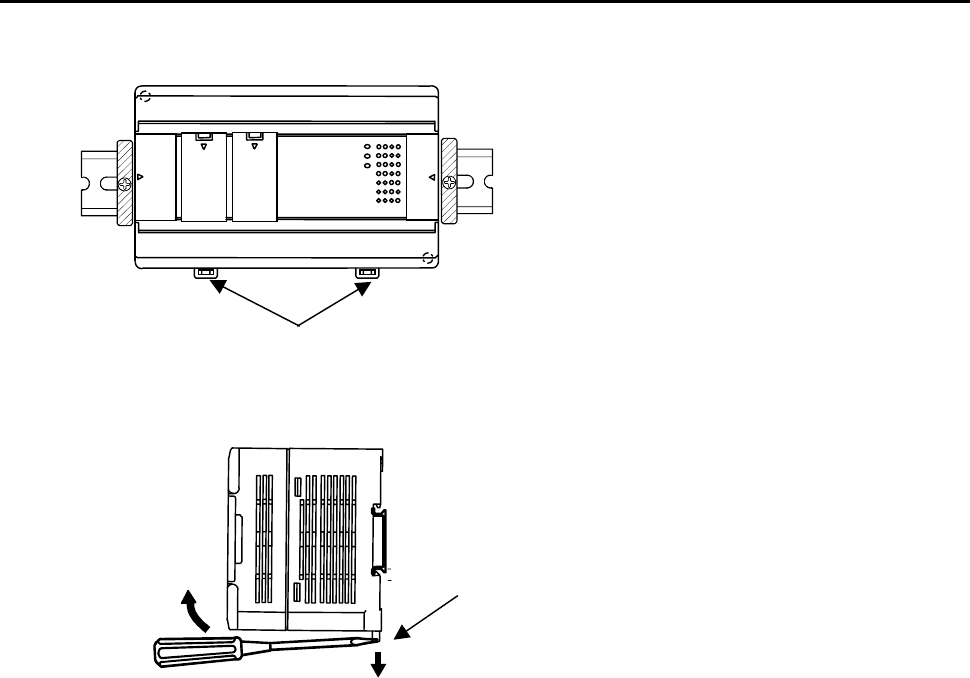
Chapter 10 PLC Installation, Mounting, Wiring
10-2
Securing the unit
Secure the unit by installing DIN rail fixing brackets
from both sides. (The product may move out of place
if not secured with the fixing brackets.)
Removing the unit from the DIN rail
1]
2]
While lowering the DIN rail attachment mounting
lever 1], lift the unit upward to remove as shown by
2].
DIN rail attachment mounting levers
DIN rail attachment mounting levers
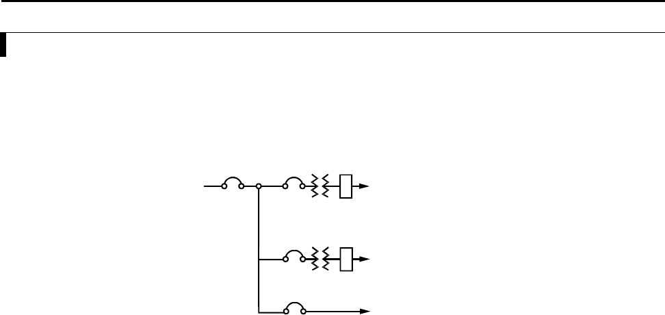
Chapter 10 PLC Installation, Mounting, Wiring
10-3
10.2 Wiring
(1) Separation of the power system
The power supplies include power for the MICRO-EH main unit/power for the I/O signals/power for general
equipment. These power supplies should be wired from separate systems as much as possible.
When these power supplies are supplied from one main power source, separate the wiring with a transformer or
similar device, so that each power supply is a separate system.
NF
100 V AC
to
240 V AC
NF
NF
Main power supply
Power for the PLC unit
Transformer
Transformer
NF: noise filter
Power for I/O signals
Power for general equipment
Figure 10.3 Example of power system diagram
(2) Regarding fail safe
1] Construct an interlock circuit external to the MICRO-EH.
When the MICRO-EH’s power is turned on or off, the inputs/outputs of the MICRO-EH may not temporarily
operate normally due to the time lag of the power supply of the MICRO-EH’s main unit, the external power
supply of the MICRO-EH’s expansion unit, and the external power supply (especially DC power supply) for
the MICRO-EH’s I/O signals, as well as the difference in their startup times.
Thus, either turn on the power to the expansion unit first, or turn on the power to both the base unit and
expansion unit simultaneously. Also, be sure to turn on the external power supply (especially DC power supply)
for the MICRO-EH’s I/O signals before turning on the MICRO-EH.
Additionally, a problem in the external power supply or a malfunction in the MICRO-EH’s main unit may
cause abnormal operations. To prevent such problems from causing abnormal operations of the entire system,
and from the viewpoint of creating a fail-safe mechanism, construct such circuits as an emergency stop circuit,
protective circuit and interlock circuit external to the MICRO-EH for the sections that may result in mechanical
damage or accident if abnormal operations occur.
2] Install a lightning arrester
To prevent damage to the equipment as a result of being struck by lightning, it is recommended that a lightning
arrester be installed for each MICRO-EH’s power supply circuit.
The MICRO-EH detects a power failure from a voltage drop in the internal 5 VDC power supply. For this
reason, when the load in the unit's internal 5 VDC system is light, 5 VDC is retained for a long period of time
and operations may continue for more than 100 ms. Thus, when an AC input unit is used, an off-delay timer for
coordinating with the internal 5 VDC system is required to avoid erroneous input since the AC input signal
turns off more quickly than the internal 5 VDC system.
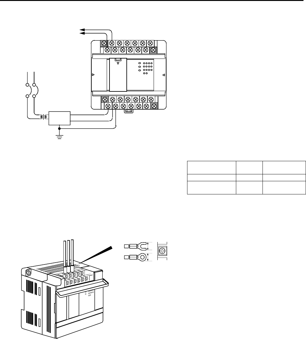
Chapter 10 PLC Installation, Mounting, Wiring
10-4
(3) Wiring to the power module
100 V AC to
240 V AC
Power supply
for the sensor
Power leakage
breaker
Shielded
insulated
transformer
Noise
filter
Figure 10.4 Power supply wiring diagram
(a) For power supply wiring, use a cable of 2
mm2 or more to prevent a voltage drop from
occurring.
(b) For the function ground terminal (PE
terminal), use a cable of 2 mm2 or more and
provide Class D grounding (100 Ω or less).
The appropriate length for the ground cable
is within 20 m.
1] Instrumentation panel and relay panel
grounding may be shared.
2] Avoid grounding shared with equipment
that may generate noise such as high-
frequency heating furnace, large-scaled
power panel (several kW or more),
thyristor exchanger, electric welders, etc.
3] Connect a noise filter (NF) to the power
cable.
(c) Tighten the terminal screws within the torque
range as shown below.
Unit Screw Clamping
torque
10-point M2.5 0.3 to 0.4 Nxm
14, 23, 28-point,
expansion M3.0 0.5 to 0.6 Nxm
(d) Use the same power supply system for the
basic and expansion units.
(4) Wiring cable for I/O signals
6
6
Tighten each terminal screw using a torque of the
specified torque range.
When using a crimp terminal, use one with an
outer diameter of 6 mm or less.
Use only up to two crimp terminals in the same
terminal. Avoid clamping down more than three
at the same time.
Only one piece of cable can be wired per
terminal if the cable type is between AWG14 and
AWG22 (cable thickness ranging between 2.1
mm2 and 0.36 mm2), but two pieces can be wired
if the cable type is between AWG16 and AWG22
(between 1.3 mm2 and 0.36 mm2).
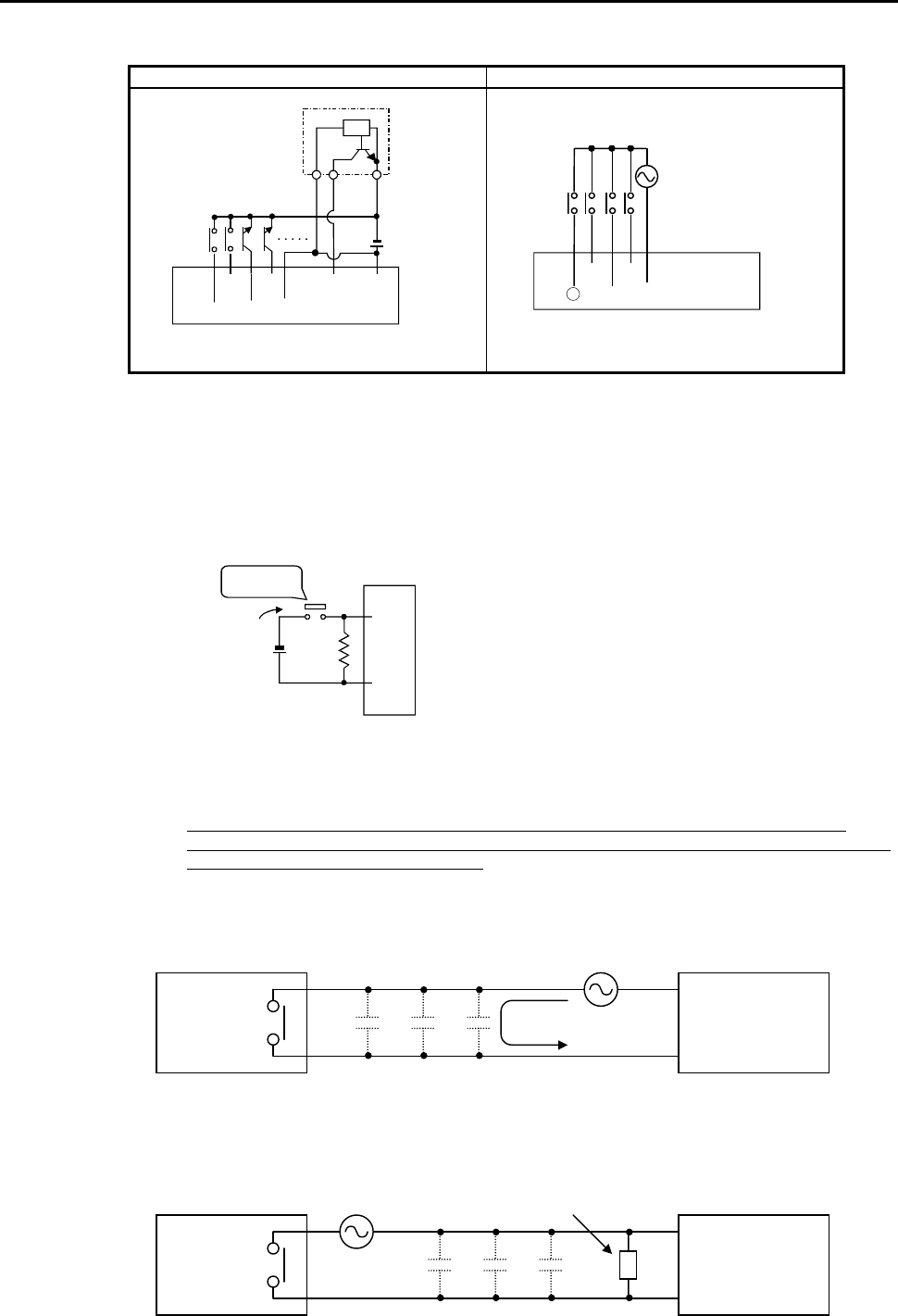
Chapter 10 PLC Installation, Mounting, Wiring
10-5
(5) Wiring to the input terminals
DC input AC input
3] 4] 6] C1
0 V C0 5] 7]
24 V DC
0]
24+
2]
1]
Current output type
Proximity switch
Example of 14-point type
③④ ⑥ C1
C0 ⑤⑦
0②
①
Example of 14-point type
Figure 10.5 Input wiring
(a) DC input
1] When all input terminals (X0, X1, ...) and the common terminal (C) are loaded with 24 VDC, the input
becomes ON status, and approximately 7.5 mA of current flows to the external input contacts.
2] For sensors such as a proximity switch or photoelectric switch, current output type (transistor open
collector) can be connected directly. For voltage-output-type sensors, connect them to the input terminal
after first going through the transistor.
3] Take measures to prevent faulty contact in a strong electric contact.
C
3 W
560 Ω
24 V DC
1]
Strong electric
contact
Approx. 50 mA
DC input module
The current that flows to a contact when external contacts
are closed is approximately 7.5 mA. If a strong electric
contact must be used, add resistance as shown in the diagram
at left and supply sufficient current to the contact to prevent
a faulty contact.
4] Limit the wiring length within 30 m.
5] Multiple number of common terminals located at each input section are not connected internally. Make
the connections externally as needed.
6] There are no RUN and STOP switches for the 10-point type. Connect with the RUN input terminal
according to the above connection procedure so that RUN and STOP can be performed. Operation cannot
be performed unless this connection is done.
(b) AC input
In case of AC input module, input voltage may exist if input wiring is long although no device drives. This
phenomenon is caused from leakage current due to floating capacitance between lines.
External
device
AC input
module
The countermeasures are [1] or [2] as follows. This voltage due to electrostatic coupling must be half of max.
OFF voltage or less.
[1] To install dummy resistor in parallel so that impedance of input module is lower.
[2] To replace power supply at drive (external device) side.
External
device
AC input
module
Dummy resistor
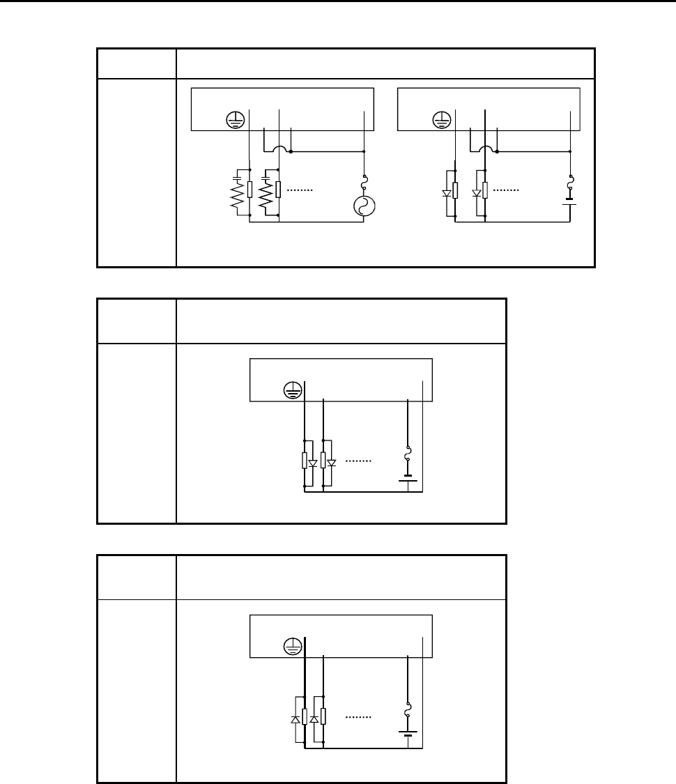
Chapter 10 PLC Installation, Mounting, Wiring
10-6
(6) Wiring to the output terminals
Item Relay output
EH-*XXDR**
External
wiring
FUSE
1] 2] 4] C2
POW C1 3] 5]
POW
C0
0]
FUSE
1] 2] 4] C2
POW C1 3] 5]
POW
C0
0]
Figure 10.6 Relay output wiring
Item
Transistor output
(sink type)
(EH-*XXDT**)
External
wiring
FUSE
NC 3] 5] C
POW 2] 4] V
POW
1]
0]
Diode
Figure 10.7 Transistor output wiring
Item
Transistor output
(source type)
(EH- XXDTP**)
External
wiring
FUSE
NC 3] 5] C
POW 2] 4] V
POW
1]
0]
Diode
Figure 10.8 Transistor output wiring
Surge killer Diode
Chapter 10 PLC Installation, Mounting, Wiring
10-7
(a) Wiring to the relay output terminals
1] Life of relay contacts
Life curve of relay contacts
500
100
10
1
01 45
50
20
63
2
1000
AC 125 V cos φ =1
AC 125 V cos φ =0.7
AC 125 V cos φ =0.4
Switching life (10,000 times)
Contact switchin
g
current
(
A
)
Figure 1 Life characteristics (125 V AC) Life of the contact is almost in squared
reverse proportion to the current, so be aware
that interrupting rush current or directly
driving the condenser load will drastically
reduce the life of the relay.
When switching is made with high
frequency, use a transistor output module.
500
100
10
1
01 45
50
20
63
2
1000
AC 250 V cos φ =1
AC 250 V cos φ =0.7
AC 250 V cos φ =0.4
Contact switchin
g
current
(
A
)
Figure 2 Life characteristics (250 V AC)
Switching life (10,000 times)
500
100
10
1
01 45
50
20
63
2
1000
DC 30 V L/R=1 ms
DV 30 V L/R=7 ms
DC 30 V L/R=15 ms
Figure 3 Life characteristics
Switching life (10,000 times)
Contact switchin
g
current
(
A
)
2] Surge killer
For inductive load, connect a surge killer (condenser 0.1 µF, + resistance of approx. 100 Ω) in parallel to
the load. Also, for DC load, connect a flywheel diode.
3] Fuse
A built-in fuse is not used in this module. Install a 6 A fuse in the common to prevent the external wiring
from burning out.
For the independent contact output section, install a 2A fuse per circuit.
(b) Wiring to the transistor output terminals
4] Flywheel diode
For inductive load, connect a flywheel diode in parallel.
5] V and C terminals
Always connect a V terminal and C (common) terminal. If the module is used without connecting these
terminals, the internal flywheel diode may not function and the module may malfunction or break down.
6] Fuse
There is no built-in fuse to prevent external wiring burning. Therefore, it is recommended that a fuse be
installed externally to prevent the external wiring from burning out. (This does not protect the internal
transistor elements.) If the external load is short-circuited, please contact us for repair.
Chapter 10 PLC Installation, Mounting, Wiring
10-8
(7) Wiring to the unit terminals
NF
Wiring for the power supply
Use a 2 mm2 cable and twist it. Leave a distance of 100
mm or more from the signal cable and 200 mm or more
from the power line.
Shield insulation
transformer
AC power supply
Connection of a noise
filter is recommended.
Use a cable 2 mm2 or
more for the wirin
g
.
Ground wiring
Class D grounding
Leave a distance of at least
200 mm from the power
line and do not run the wire
next to the power cable.
I/O signal cable
Ex
p
ansion cable
Always segregate power
line, I/O signal and
power supply cable
Metal plate
Perform class D grounding
Outer hull (Cabinet)
Perform class D grounding
Figure 10.9 Example of wiring
(8) Wiring to the analog I/O terminals
•Do not apply the voltage that exceeds the rated input voltage to the analog input terminals. In addition, do not
allow the current that exceeds the rated input current to flow into the analog input terminals. If a power supply
that is different from the specified power supply is connected, the product may be damaged or burned out.
•For the channels that do not use the analog input terminals, be sure to short-circuit the analog input terminals
before using such channels.
•For the external wiring to the analog I/O terminals, use a shielded cable and make routing different from other
power lines with different voltages and signal lines. In addition, ground one end of the shield cable. However,
grounding both ends or open ends may have better effect than grounding one end of the shield cable, depending
on the noise environment in which the equipment is used. Use the appropriate grounding method accordingly.
•Place AC power supply lines, signal lines and data lines in separate pipes.
•Wire signal lines and data lines as close as possible to a grounded surface such as a cabinet and metal bar.
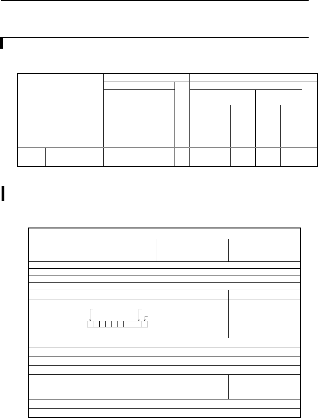
Chapter 11 Communication Specifications
11-1
Chapter 11 Communication Specifications
11.1 Port function
Port function of MICRO-EH is shown in Table 11.1.
Table 11.1 Communication port specification
RS-232C RS-422/485
Dedicated port Dedicated port
Transmission procedure 1 Transmission
procedure 2
Port type
Transmission
procedure 1
Trans.
proce-
dure 2 Without St. No.
(1:1)
With
St. No.
(1:N)
Without
St. No.
(1:1)
With
St. No.
(1:N)
Connected devices Programming device,
PC, modem, HMI
PC,
etc.
PC,
etc.
Programming
device, PC, HMI PC, etc. PC, etc. PC,
etc.
PC,
etc.
Port 1 All modules 999*- ----
Port 2 23,28 pts. module - - - 99999*
* Supported by software version 1.30 (WRF051=H0130) or newer.
11.2 Port 1
Specification of port 1 is shown below.
Table 11.1 Port 1 specification
Item Specification
Communication Dedicated (programming) port Modem mode General purpose port
speed* 4800, 9600, 19.2k, 38.4k bps
2400, 4800, 9600, 19.2 k, 38.4k,
57.6 k bps
300, 600, 1200, 2400, 4800,
9600, 19.2k, 38.4k, 57.6k bps
Communication system Half duplex
Synchronization Asynchronous
Startup system One-sided startup using the host side command
Transmission system Serial transmission (bit serial transmission)
Transmission code ASCII Configured by user
Transmission code
configuration
ASCII: 7-bit data, 1 start, 1 stop, even parity
202126P
Start bit (1 bit) Parity bit (1 bit)
Stop bit (1 bit)
Data (7 bits) (even parity)
Configured by user
Data sending sequence Sent out from the lowest bit
Error control Vertical parity check, checksum, overrun check, framing check
Transmission unit Message unit (variable length)
Max. message length 1,024 bytes (including control characters)
Control procedure H-series dedicated procedure (hi-protocol)
Standard protocol (transmission control procedure 1),
Simplified protocol (transmission control procedure 2)
Configured by user
Interface RS-232C (maximum cable length: 15 m)
Connector 8P modular connector (RJ45)
* : Handy programmers are not available with MICRO-EH.
* : GPCL01H is not available with 10 points type as communication speed is fixed as 4,800 bps.
* : If host sends NAK command, the next message must be sent after 10 ms interval.
General purpose
p
ort
General purpose
p
ort
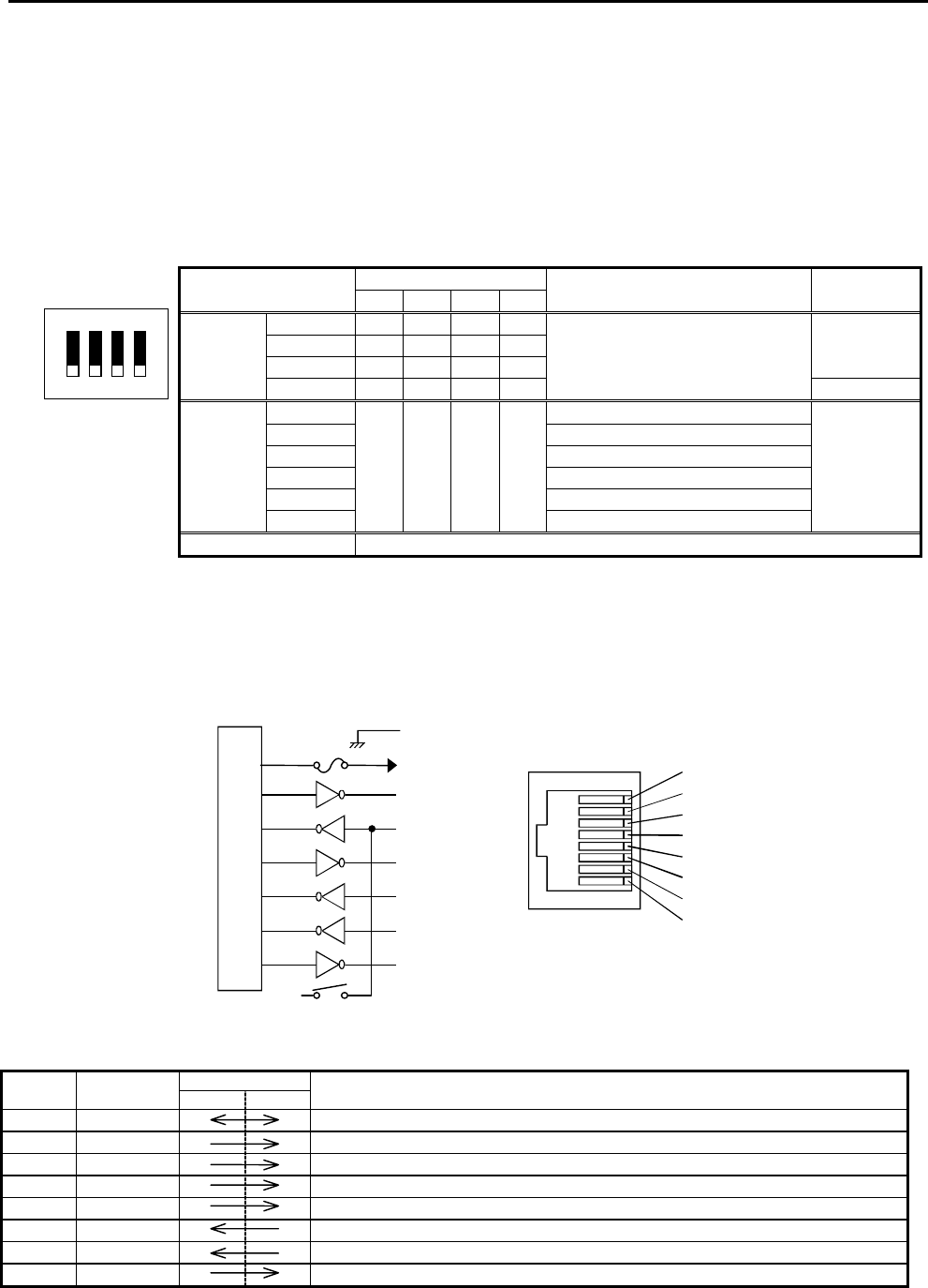
Chapter 11 Communication Specifications
11-2
(1) Port 1 settings
Port 1 is configured by combination of DIP switch and special register (WRF01A).
DIP switch can be set when cable is not connected (DR signal is off). Switch configuration is set at cable connected
(DR is high).
Value in WRF01A is saved in FLASH memory when writing flag (R7F6) is turned on. If saved in FLASH memory,
it is not necessary to set again at the next power up.
[ Caution ] If transmission procedure 2 is configured and saved in FLASH memory once, peripheral
device/application which supports procedure 1 such as LADDER EDITOR can not be connected.
DIP switch
Port type 1234 WRF01A Remarks
38.4 kbps ON off ON off
19.2 kbps ON off off off
9600 bps off off ON off
Dedicated
port
4800 bps off off off off
H0000 : Transmission procedure 1
H8000 : Transmission procedure 2
Default
4800 bps H0000 : Prcd. 1 / H8000 : Prcd. 2
9600 bps H0100 : Prcd. 1 / H8100 : Prcd. 2
19.2 k bps H0200 : Prcd. 1 / H8200 : Prcd. 2
38.4 k bps H0300 : Prcd. 1 / H8300 : Prcd. 2
57.6 k bps H0400 : Prcd. 1 / H8400 : Prcd. 2
Dedicated
port via
modem
2400 bps
off ON off off
H0500 : Prcd. 1 / H8500 : Prcd. 2
H0*** :
Procedure 1
H8*** :
Procedure 2
General purpose port Port switching by FUN5 command, Baud rate by TRNS/RECV command
* Due to no DIP switch equipped, 10 points type does not support modem function.
* +12V is supplied from pin 4 if DIP switch is ON.
* General purpose port is supported by software version 0130 (WRF051=H0130) or newer.
(2) Port 1 hardware
The circuit diagram of port 1 and the signal list are shown in Figure 11.2 and Table 11.3 respectively.
Figure 11.2 Circuit diagram and pin numbers for port 1
Table 11.3 List of port 1 signals
Pin No. Signal Direction Meaning
abbreviation CPU Host
1] SG1 Signal ground
2] VCC 5 V DC is supplied. (Protective fuse is connected.)
3] DTR1 (ER) Communication enabled signal. When it is high, communication is possible.
4] CD1 (DCD) 12V is output when DIP switch 1 is on.
5] SD1 (TXD) Data sent by the CPU
6] RD1 (RXD) Data received by the CPU
7] DR1 (DSR) Peripheral units connected signal. When it is high, peripheral device is connected.
8] RS1 (RTS) Transmission request signal. When it is high, CPU is ready to receive data.
TX1
RX1
DR1
RS1
1] SG1
2] VCC
3] DTR1
4] CD1
5] SD1
6] RD1
7] DR1
8] RS1
12 V
5 V
ER1
DCD1
Micro processor
1]
2]
3]
4]
5]
6]
7]
8]
4321
ON
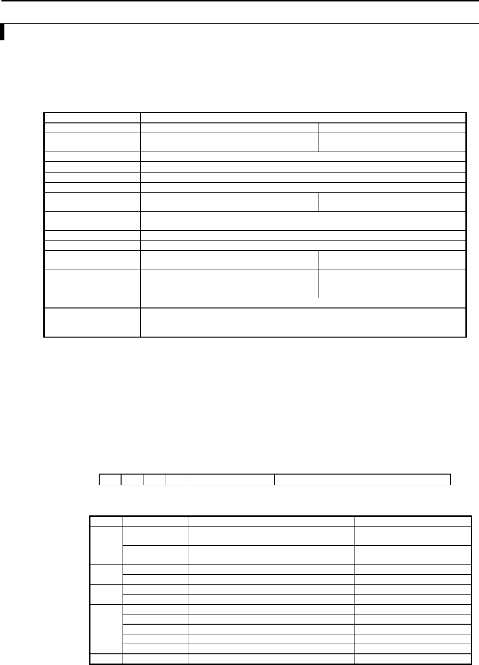
Chapter 11 Communication Specifications
11-3
11.3 Port 2
The specifications of port 2 are listed in Table 11.4. 1:n station communication by the high protocol is possible with port 2.
By creating and including a control procedure based on the high protocol on the personal computer which will become the
host, it becomes possible to control a maximum of 32 stations from one host. The systems can thus be configured in several
ways.
Table 11.4 Port 2 specifications
Item Specification
Dedicated (programming) port General purpose port
Communication speed 4800, 9600, 19.2 k, 38.4 k bps 300, 600, 1200, 2400, 4800, 9600, 19.2 k,
38.4 k, 57.6 k bps
Communication system Half duplex
Synchronization Asynchronous
Startup system One-sided startup using the host side command
Transmission system Serial transmission (bit serial transmission)
Transmission code,
configuration
ASCII: 7-bit data, 1 start, 1 stop, even parity Configured by user
Transmission code outgoing
sequence
Sent out from the lowest bit in character units
Error control Vertical parity check, checksum, overrun check, framing check
Transmission unit Message unit (variable length)
Maximum message length 503 bytes (including control characters)
Note: 505 bytes when the station number is used.
1,024 bytes
Control procedure H-series dedicated procedure (h-protocol)
Standard protocol (transmission control procedure 1),
Simplified protocol (transmission control procedure 2)
Configured by user
Interface RS-422/485 (maximum cable length: 250 m)
Connector CPU side: 15-pin D-sub
Cable side: a cable equivalent to 17JE-23150-02(D8B) (DDK Co., Ltd.) is recommended (D-SUB
fitting screw M3 × 0.5)
(1) Setting port 2
Port 2 is configured by special register WRF03D. The settings can be changed even when port 2 is communicating. The
highest bit (b15) of WRF03D is setting bit.
If station number mode is used, make sure to set the station number from 0 to 31 in BCD code.
Value in WRF03D is saved in FLASH memory when writing flag (R7F6) is turned on. If saved in FLASH memory, it is
not necessary to set again at the next power up.
(Example) Transmission control procedure 2, communication speed 19.2 kbps, and station number 28.
Î WRF03D = HE228 After the setting is completed, WRF03D is changed to H6228. (b15 cleared)
Bit: 1514131211109876543210
WRF03D: abc0 d e
Initial value: 0000000000000000
Figure 11.3 Special internal output for setting port 2
Field Setting value Content Note
a 0 Setting completed After the setting is completed, the
system changes this bit to 0.
1 Setting change request Set this bit to 1 when changing the
setting.
b 0 Transmission control procedure 1
1 Transmission control procedure 2
c 0 Without station number
1 With station number
d 0 Transmission speed 4800 bps Setting of bits 8 to 12 H0000
1 9600 bps H0001
2 19.2 kbps H0010
3 38.4 kbps H0011
Other than above 4800 bps
e 0 ~ 31 Station number * Set by BCD.
* Communication speed of general purpose port is configured in TRNS/RECV command. Value in WRF03D
is ignored.
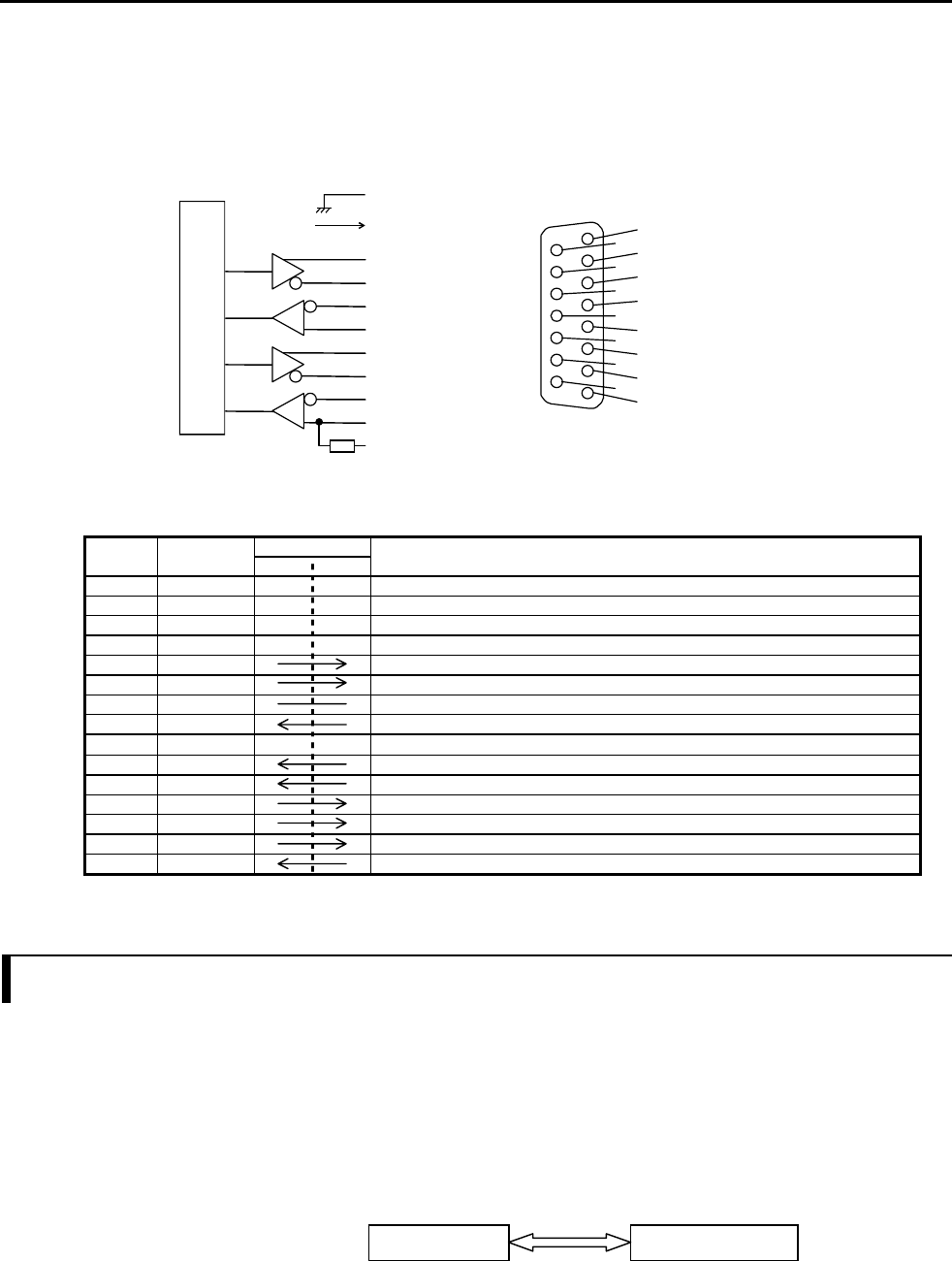
Chapter 11 Communication Specifications
11-4
(2) 1:n station communication on RS-485
When station number mode is used on RS-485, termination command (NAK FF) from host/PC can conflict with reply
from CPU, and CPU can fail to receive this command. Pay attention to this possibility at using this command.
(3) Port 2 hardware
The circuit diagram of port 2 and the signal list are shown in Figure 11.4 and Table 11.6 respectively.
Figure 11.4 Circuit diagram and pin numbers for port 2
Table 11.6 List of port 2 signals
Pin No. Signal Direction Meaning
abbreviation CPU Host
1] NC Not used
2] NC Not used
3] NC Not used
4] NC Not used
5] Vcc 5 V DC is supplied.
6] RSN Transmission request signal. When it is high low, CPU is ready to receive data..
7] SG Signal ground
8] CSP Receive enabled signal. When it is high, connected device is ready to receive data.
9] RT Terminating resistor (120Ω). Connect to pin 10 if necessary.
10] RDN Data received by the CPU -
11] RDP Data received by the CPU +
12] SDN Data sent by the CPU -
13] SDP Data sent by the CPU +
14] RSP Transmission request signal. When it is high level, CPU is ready to receive data.
15] CSN Receive enabled signal. When it is low, connected device is ready to receive data.
11.4 General purpose port (Port 1,2)
General purpose port can be configured either port 1 or port 2 by FUN 5 command in user program. General purpose port
enables serial communication to devices like bar code reader by TRNS/RECV command in user program.
Even if configured, the port works as general purpose port only CPU is in RUN status. Port is changed back to dedicated
port when CPU is in STOP status.
* General purpose port is supported by software version 1.30 (WRF051=H0130) or newer.
TX2
RX2
CS2
RS2
VCC
7] SG
5] VCC
14] RSP
6] RSN
15] CSN
8] CSP
13] SDP
12] SDN
10] RDN
11] RDP
9] RT
Micro processor
9]
10]
11]
12]
13]
14]
15]
1]
2]
3]
4]
5]
6]
7]
8]
General purpose port Dedicated port
CPU in STOP
General purpose port
CPU in RUN
Switching
automatically
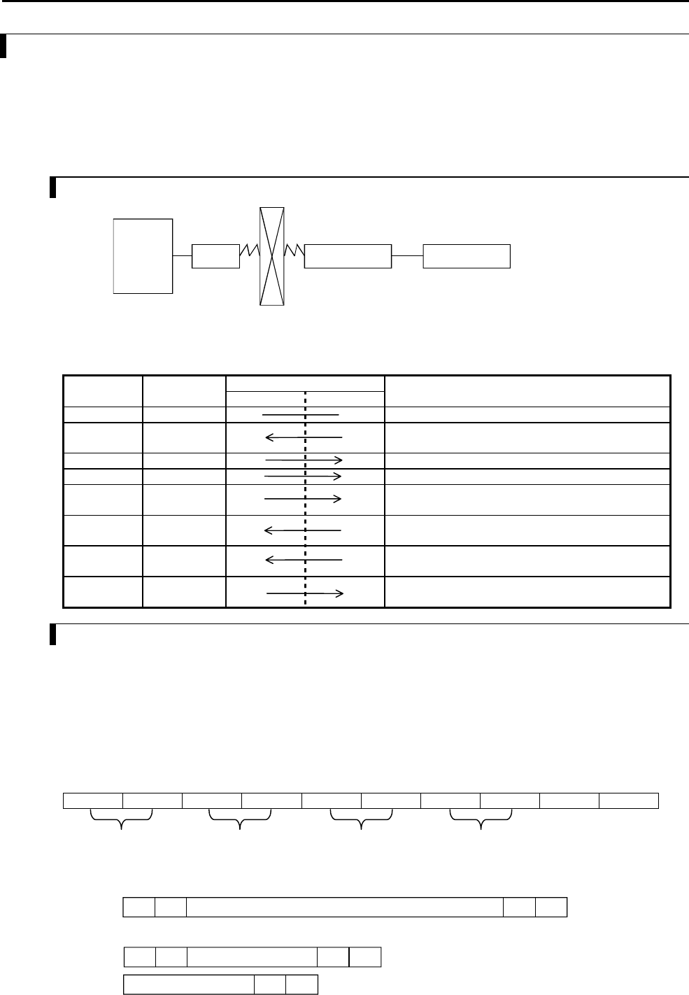
Chapter 11 Communication Specifications
11-5
11.5 Modem Control Function
The 14-point or higher MICRO-EH is equipped with a modem control function. The modem control function can be
operated using task codes. To use this function, it is necessary to set No.2 of the DIP SW.
For details on the communication specifications, see Table 11.1, “Specifications of port 1.”
* The 10-point type CPU does not have this function.
Connecting two operating modems may be difficult if there is a significant difference between them in terms of
communication speeds. Thus, use the models having the same communication speed.
11.5.1 Configuration
Figure 11.5 Modem connection configuration diagram
Table 11.7 List of port 1 signals when a modem is connected
Pin No. Signal Direction
abbreviation CPU Host Meaning
1] SG1 Signal ground
2] CD1 Carrier receive in-progress notification signal
Connected to CD in the modem.
3] ER1 Communication enabled signal of the terminal
4] ER2 Not used
5] SD1 Data sent by the CPU
Connected to SD in the modem.
6] RD1 Data received by the CPU
Connected to RD in the modem.
7] DR1 Communication enabled signal of the modem
Connected to DR in the modem.
8] RS1 Transmission request signal
Connected to RS in the modem.
11.5.2 AT Commands
The AT commands are used to make various modem settings, and are set from the host computer. The MICRO-EH issues
the AT commands automatically for initial setting. Other than this, the AT commands are not used.
Refer to instruction manual or other documents furnished by modem manufacturers for details on the AT commands.
In AT commands, an instruction sent to the modem from the host is called a “command,” and the character string in
response to the “command” returned to the host from the modem is called a “result code.”
AT commands always begin with the character string “AT,” and a return code is input at the end of the command. However,
A/ is excluded. The command that follows the “AT” can have multiple inputs in a single line.
Example)
AT&C1&S0 P 2CRLF
(1) Format
1] AT command format
LFCRAT command parameter command parameter · · · ·
2] Result code format
CR LF CR LF
CR LF
Result code (word)
Result code (number)
AT commands CD signals: Follows the
carrier signals generated
by the opposite device
DR signals: Always On 20 pps (pulse setting)
MICRO-EH
RS-232C
(MAX 57.6 kbps)
Personal
computer Modem Modem
Public line

Chapter 11 Communication Specifications
11-6
(2) List of commands (extract)
1] AT commands
Command Function overview Example
AT Automatically recognizes data format
A/ Re-executes the response directly preceding
ATA Forced reception
ATDmm Dial ATD12345678
ATEn Command echo (echo back a text string entered to modem) 0: No
1: Yes
ATE0
ATHn Line ON/OFF 0: On hook (disconnect)
1: Off hook
ATH0
ATH1
ATPn Pulse (dial) setting 0, 1: 10 pps
2 : 20 pps
ATP0, ATP1
ATP2
ATQn Result code setting 0: Yes 1: No ATQ0
ATT Tone (push) setting ATT
ATSn = X Sets S register value. ATS0 = 0
ATVn Result code display format 0: Number
1: Word
ATV0
ATV1
AT&Cn CD signal control 0: Always on
1: Depends on the carrier of counter-party modem
AT&C0
AT&C1
AT&Dn ER signal control
0: Always on
2: Turning from on to off during communication disconnects line
3: Turning from on to off resets the software
AT&D0
AT&D2
AT&D3
AT&Sn DR signal 0: Always on
1: Depends on sequence
2: Depends on CD signal
AT&S0
AT&S1
AT&S2
AT&Rn RI(CI) signal control
0: Turns on from calling start until communication begins
1: Turns on from calling start until communication ends
2: Turns on/off in synchronization with the call signal
AT&R0
AT&R1
AT&R2
2] S register
S register Set value Function
S0 0 no automatic
reception
1 to 255
Setting for automatic reception/reception ring count
S2 0 to 127
(43 [+] )
Escape code setting
S3 0 to 127
(13 [CR] )
CR code setting
S4 0 to 127
(10 [LF] )
LF code setting
3] Result codes
Number format Word format Meaning
0 OK Normal execution
1 CONNECT Connection complete
2 RING Reception detected
3 NO CARRIER Line disconnected
4 ERROR Command error
5 CONNECT 1200 1200 bps connection
6 NO DIAL TONE Cannot hear dial tone
7 BUSY Busy signal detected
8 NO ANSWER No tone heard
10 CONNECT 2400 2400 bps connection
11 CONNECT 4800 4800 bps connection
12 CONNECT 9600 9600 bps connection
13 CONNECT 14400 14400 bps connection
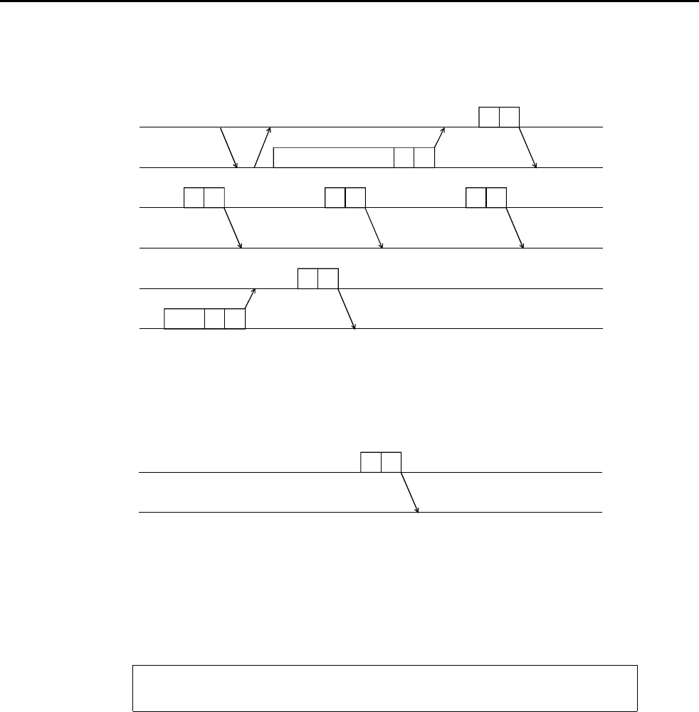
Chapter 11 Communication Specifications
11-7
(3) Sequence
An example of a communication sequence using the Omron-made modem ME3314A is given below.
(a) Reception sequence
MICRO-EH
MICRO-EH
MICRO-EH
ATE0Q0V0&C1&S0 CR LF
0CR
2CR
3]
2CR2CR
1CR
ATA C R L F
ER on
Modem
Modem
Modem
Waiting for reception
Forced connection when three rings are detected
Reception complete
Port communication begins from here
DR on
Initial setting (Note 1)
1]
2]
4]
1] The PLC issues the AT command that performs the initial setting of the modem.
2] If initial setting is OK, the modem returns “0.”
3] The PLC detects the result code “2” three times while in the reception wait state.
4] It connects the modem.
(b) Disconnect sequence
MICRO-EH
3CR
M
odem
Line disconnected
Port communication ends 1]
1] The PLC disconnects the line when the result code “3” is returned from the modem.
Note 1: Since the modem initial setup sets only minimal items from the MICRO-EH side, connect a personal computer
and perform necessary settings before making the connection. (Set the DR signal to always on.) Moreover, do not
change the following initial settings.
Contents of the initial settings
Command echo: None
Result code: Yes
Display format of result code: Numerical format
Note 2: The modem timeout (WRF03C) stored in the special internal output refers to the time from data transmission
from the MICRO-EH to the data reception from the opposite station (STX, ENQ, NAK). Normally, this special
internal output should be set to “0000” (default) or “H8000” (no timeout). Set the timeout only when it is
especially necessary to monitor the reception time from the opposite station. When a timeout is detected, the
MICRO-EH cuts off the line. When setting the timeout, set the time in the ** part of H80. The unit is * seconds
(hexadecimal).
Note 3: Before actually cutting off the line, issue the task code of the line cut off request (HIC--see Appendix 2, “Task
code list” for details) from the host side.
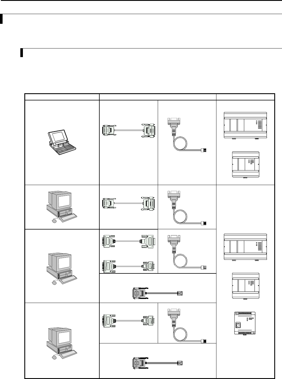
Chapter 11 Communication Specifications
11-8
11.6 Connecting to the Ports
The following shows some examples of connections between port 1 and 2 and peripheral units. When creating a
connection cable, check it thoroughly in advance according to what the purpose of its use is.
11.6.1 Port 1
Port 1 of the MICRO-EH is a communication port that uses the RS-232C protocol as interface. It is also a dedicated port
with which to perform communication by the H series dedicated procedure (high protocol). Table 11.8 lists the types of
peripheral units and cables that can be connected to port 1.
Table 11.8 Peripheral unit connection configuration
Peripheral unit Cable CPU type
28-/23-point type
GPCL01H
(Ladder Editor, HI-Ladder)
GPCB02H
EH-RS05
14-point type
Ladder Editor (DOS version)
PCCB02H
EH-RS05
WPCB02H (PC9800)
WVCB02H
(DOS/V system)
EH-RS05
Ladder Editor for Windows®
EH-VCB02 (DOS/V system)
WVCB02H
EH-RS05
Pro-H
EH-VCB02
28-/23-point type
14-point type
10-point type
*1: Set the DIP switches to 19.2 kbps when connecting to a GPCL01H.
*2: Adjust the DIP switch settings to the speed with which to communicate when connecting a LADDER EDITOR or
Pro-H. (The speed is fixed at 4800 bps for 10-point type CPU.)
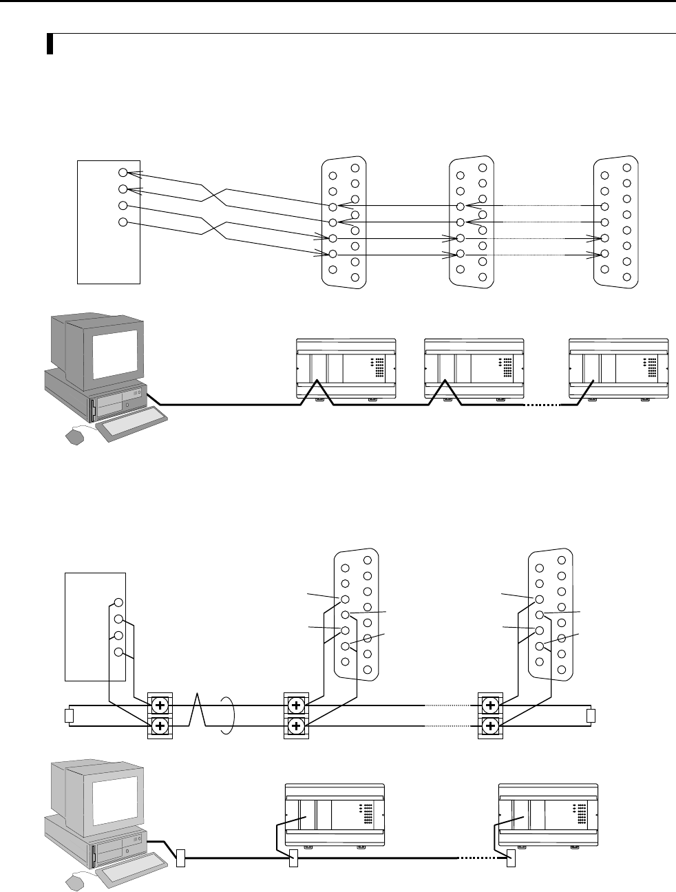
Chapter 11 Communication Specifications
11-9
11.6.2 Port 2
Port 2 of the MICRO-EH is a communication port that uses either the RS-422 or RS-485 protocol as interface. It is also a
dedicated port with which to perform communication by the H series dedicated procedure (high protocol), which allows
1:n station communication. Figure 11.6 and 11.7 show examples of port 2 connections for 1:n station communication.
Moreover, the connection for communicating 1:1 is performed by connecting only the first CPU in the figure below.
(1) In case of RS-422
MICRO-EH
(32nd CPU)
MICRO-EH
(2nd CPU)
MICRO-EH
(1st CPU)
Host
RD (+)
RD (-)
SD (-)
SD (+)
(13) SDP
(12) SDN
(11) RDP
(10) RDN
(13) SDP
(12) SDN
(11) RDP
(10) RDN
(13) SDP
(12) SDN
(11) RDP
(10) RDN
Figure 11.6 Connection for 1:n station communication by RS-422
(2) In case of RS-485
Relay terminal blockRelay terminal block
Twisted pair cable
Relay terminal block
MICRO-EH
(1st CPU)
Host
RD (+)
RD (-)
SD (-)
SD (+)
B
A
MICRO-EH
(32nd CPU)
(13) SDP
(12) SDN
(11) RDP (10) RDN
(13) SDP
(12) SDN
(11) RDP (10) RDN
Figure 11.7 Connection for 1:n station communication by RS-485

Chapter 11 Communication Specifications
11-10
MEMO
Chapter 12 Error Code List and Special Internal Outputs
12-1
Chapter 12 Error Code List and Special Internal
Outputs
12.1 Error Codes
The table below indicates the self-diagnostic error codes. (See Chapter 13, “Troubleshooting” about corrective actions.)
Error codes are output as hexadecimal values to the special internal output WRF000. (This special internal output is
saved during power failure, and is retained even when the causes of the error are eliminated. Also, when multiple errors
occur, the most fatal error in the error classification is stored.)
Note: LED examples The occurrence of a flashing pattern other than the following means a micro computer error.
However, an error code is not reflected in the special internal output in this case.
: ON : OFF : Flashing (1 s ON, 1 s OFF) : Flashing (500 ms ON, 500 ms OFF) : Flashing (250 ms ON, 250 ms OFF)
Related special
internal output
Error
code
Error name
[detection timing]
Classifi
-cation Description RUN
LED
OK
LED
Ope-
ration Bit Word
11 System ROM error
[at power ON]
Fatal
error
The system ROM has a checksum
error or cannot be read
Error in built-in ROM/FLASH )
Stop
12 System RAM error
[at power ON]
Fatal
error
The system RAM cannot be read
and/or written properly
Stop
13 Micro computer error
[always checking]
Fatal
error
Address error interrupt, undefined
instruction interrupt occurred in the
micro computer
Stop R7C8
Reset processing in
progress
[at power ON]
CPU is being reset. Stop
1F System program error
[always checking]
Fatal
error
System program in FLASH memory
has a checksum error
Stop
23 Undefined instruction
[at starting RUN]
Serious
error
Error is detected when an attempt is
made to execute a user program
instruction that cannot be decoded
(undefined instruction)
Stop R7C9
27 Data memory error
[at power ON and
initializing CPU]
Serious
error
Data memory cannot be read/written
properly.
Stop
31 User memory error
[at power ON and during
RUN]
Serious
error
A checksum error is detected in user
memory.
Stop R7CA
33 User memory size error
[at starting RUN]
Serious
error
User program capacity set by the
parameter is other than 280 HEX.
Stop R7CC
34 Grammar/assemble error
[at starting RUN and
online change in RUN]
Serious
error
There is a grammatical error in user
program.
Stop R7D4 WRF001
41 I/O configuration error
[always checking]
Minor
error
• I/O assignment information and
actual loading of module do not
match
• Assignment is made for expansion
level 5 or greater.
• There exists assignment of 5 slots or
greater.
*1 Stop
*2
R7CD WRF002
44 Overload error
(normal scan)
[at END processing]
Minor
error
Execution time for normal scan
exceeded the overload check time set
by the parameter.
*1 Stop
*2
R7D1
45 Overload error
(periodical scan)
[periodical processing]
Minor
error
Execution time for periodical scan
exceeded the execution period.
*1 Stop
*2
R7D2
46 Overload error
(interrupt scan)
[during interrupt
processing]
Minor
error
An interrupt of the same cause
occurred during interrupt scan
*1 Stop
*2
R7D3
Chapter 12 Error Code List and Special Internal Outputs
12-2
Related special
internal output
Error
code
Error name
[detection timing]
Classifi
-cation Description RUN
LED
OK
LED
Ope-
ration Bit Word
5F Backup memory error
[at program downloading
and special I/O function
setting is requested]
Warning Data cannot be written to the backup
memory.
*1 Run
61 Port 1 transmission error
(parity)
[when transmitting]
Warning Parity error was detected during
transmission.
*1 Run
62 Port 1 transmission error
(framing/overrun)
[when transmitting]
Warning Framing error or overrun error was
detected during transmission.
*1 Run
63 Port 1 transmission error
(time out)
[when transmitting]
Warning Time out error was detected during
transmission.
*1 Run
64 Port 1 transmission error
(protocol error)
[when transmitting]
Warning Protocol (transmission procedure)
error was detected during transmission.
*1 Runs
65 Port 1 transmission error
(BCC error)
[when transmitting]
Warning Checksum error was detected during
transmission.
*1 Run
67 Port 2 transmission error
(parity)
[when transmitting]
Warning Parity error was detected during
transmission.
*1 Run
68 Port 2 transmission error
(framing/overrun)
[when transmitting]
Warning Framing error or overrun error was
detected during transmission.
*1 Run
69 Port 2 transmission error
(time out)
[when transmitting]
Warning Time out error was detected during
transmission.
*1 Run
6A Port 2 transmission error
(protocol error)
[when transmitting]
Warning Protocol (transmission procedure)
error was detected during transmission.
*1 Run
6B Port 2 transmission error
(BCC error)
[when transmitting]
Warning Checksum error was detected during
transmission.
*1 Run
71
*3
Battery error
(data memory)
[always checking]
Warning •Battery voltage dropped below the
specified value
•Battery not installed
*1 Run R7D9
72
*4
Instantaneous power
failure detection
[always checking]
Warning Instantaneous power failure detected. *1 Run R7CF
R7DA
94 Port 1
No modem response
[when modem is
connected]
Warning There is no response with the AT
command.
*1 Run
*1: Depends on the CPU’s operating state. The RUN LED is lit while the CPU is in operation; the RUN LED is unlit while the
CPU is not in operation.
*2: Depending on the settings of the operating parameters from the peripherals, the operation may be continued even when an error
occurs.
*3: Although batteries cannot be mounted on the 10- or 14-point type, battery errors are monitored by the system. Set R7EE to
OFF prior to the use.
*4: Supported by software version 1.11 (WRF051=H0111) or newer.
How to Clear the CPU Error Code:
Set 1 to the Special Internal Output R7EC.

Chapter 12 Error Code List and Special Internal Outputs
12-3
12.2 Syntax and Assembler Error Codes
The following describes the syntax and Assembler error codes. The error codes are output as hexadecimal values to the
internal output WRF001. The syntax and Assembler error checks are performed at the time of RUN startup.
Error code Error item Description of error Corrective action
H0001 Duplicate definition of
LBL
There are 2 or more LBL instructions with the
same number in the program
Limit the LBL instruction that has
2 or more of the same number to 1.
H0002 Duplicate definition of
FOR
There are 2 or more FOR instructions with the
same number in the program
Limit the FOR instruction that has
2 or more of the same number to 1.
H0003 Duplicate definition of
NEXT
There are 2 or more NEXT instructions with the
same number in the program
Limit the NEXT instruction that
has 2 or more of the same number
to 1.
H0004 Duplicate definition of
SB
There are 2 or more SB instructions with the same
number in the program
Limit the SB instruction that has 2
or more of the same number to 1.
H0005 Duplicate definition of
INT
There are 2 or more INT instructions with the
same number in the program
Limit the INT instruction that has
2 or more of the same number to 1.
H0010 END undefined There is no END instruction prior to the INT or
SB instructions
Define the END instruction before
the INT or SB instruction.
H0011 RTS undefined There is no RTS instruction corresponding to the
SB instruction
Define the RTS instruction after
the SB instruction.
H0012 RTI undefined There is no RTI instruction corresponding to the
INT instruction
Define the RTI instruction after the
INT instruction.
H0013 SB undefined There is no SB instruction corresponding to the
RTS instruction
Define the SB instruction before
the RTS instruction.
H0014 INT undefined There is no INT instruction corresponding to the
RTI instruction
Define the INT instruction before
the RTI instruction.
H0020 RTS area error There is the RTS instruction in the normal scan
area or interrupt scan program area
Define the RTS instruction within
the subroutine area.
H0021 RTI area error There is the RTI instruction in the normal scan
area or subroutine program area
Define the RTI instruction within
the interrupt scan area.
H0022 END area error There is the END instruction in the interrupt scan
program area or subroutine program area
Define the END instruction at the
end of the normal scan area.
H0023 CEND area error There is the CEND instruction in the interrupt
scan program area or subroutine program area
Define the CEND instruction
within the normal scan area.
H0030 RTS start condition error There is a startup condition in the processing box
that includes the RTS instruction
Delete the startup condition of the
processing box.
H0031 RTI start condition error There is a startup condition in the processing box
that includes the RTI instruction
Delete the startup condition of the
processing box.
H0032 END start condition error There is a startup condition in the processing box
that includes the END instruction
Delete the startup condition of the
processing box.
Syntax and Assembler error checks by the task code
The undefined contents of the syntax, Assembler and operation error codes will be checked.
However, error codes will not be set in WRF001

Chapter 12 Error Code List and Special Internal Outputs
12-4
12.3 Operation Error Codes
If an error occurs when a control instruction is executed, “1” is set in the operation error (ERR) special internal output
“R7F3” and an error code (hexadecimal) indicating the description of the error is set in WRF015.
To clear the operation errors to zeros, execute “R7F3=0” using a forced setting from a program or peripheral unit. To
clear the error codes to zeros, execute “WRF015=0” using a forced setting from a program or peripheral unit.
Error code Error name Description of error Originating
instruction
H0013 SB undefined SBn instruction corresponding to the instruction
number n in the CALn instruction is not
programmed
CAL
H0015 LBL undefined LBLn instruction corresponding to the instruction
number n in the JMPn and CJMPn instructions is
not programmed
JMP
CJMP
H0016 FOR undefined FORn instruction corresponding to the instruction
number n in the NEXTn instruction is not
programmed
NEXT
H0017 NEXT undefined NEXTn instruction corresponding to the
instruction number n in the FORn instruction is
not programmed
FOR
H0040 LBL area error LBLn instruction corresponding to the instruction
number n in the JMPn and CJMPn instructions is
not programmed in the same program area
JMP
CJMP
H0041 CAL nesting overflow There are more than 6 levels of subroutine nesting CAL
H0042 CAL undefined RTS instruction was executed without executing
the CAL instruction
RTS
H0043 FOR to NEXT error There is a NEXTn with the same instruction
number n prior to the FORn instruction
FOR
H0044 NEXT area error There is no NEXTn instruction with the same
instruction number n as the FORn instruction in
the same program area
FOR
H0045 FOR to NEXT nesting
overflow
The FORn and NEXTn instructions are not nested FOR
H0046 FOR nesting overflow There are more than 6 nesting levels of FOR to
NEXT
FOR
NEXT

Chapter 12 Error Code List and Special Internal Outputs
12-5
12.4 Bit Special Internal Output Area
The MICRO-EH has a special internal output area for performing status display and various other settings. The special
internal output area is constantly backed up in case of power failure.
The following lists the definitions of the bit special internal output area (R7C0 to R7FF).
No. Name Meaning Description Setting
condition
Resetting
condition
R7C0 Ignore scan time
error (normal scan)
0: Stop operation
1: Continue operation
Designates continue/stop running when
a normal scan overload error occurs
R7C1 Ignore scan time
error (cyclic scan)
0: Stop operation
1: Continue operation
Designates continue/stop running when
a periodic-scan overload error occurs Set by user
R7C2 Ignore scan time
error (interrupt scan)
0: Stop operation
1: Continue operation
Designates continue/stop running when
an interrupt-scan overload error occurs
Cleared by
user, Cleared
when
retentive area
is cleared, or
the CPU is
initialized.
R7C3 Undefined Do not use.
R7C4 Undefined Do not use.
R7C5 Undefined Do not use.
R7C6 Undefined Do not use.
R7C7 On line change in
RUN
0: On line changed not
allowed.
1: On line changed
allowed.
Designates whether online change in
RUN is allowed in user program Set by user
R7C8 Serious error flag 0: Normal
1: Abnormal
Indicates whether there is an abnormal
in the microcomputer
(Address error, undefined instruction)
R7C9 Microcomputer error 0: Normal
1: Abnormal
Indicates whether there is an abnormal
in the microcomputer
(Computation error)
R7CA User memory error 0: Normal
1: Abnormal
Indicates whether there is an abnormal
in user memory
Set by the
system
Cleared by
user, Cleared
when
retentive area
is cleared, or
the CPU is
initialized.
R7CB Undefined Do not use.
R7CC Memory size over 0: Normal
1: Abnormal
Indicates whether the capacity set by
the parameter exceeds loaded memory
capacity
R7CD I/O configuration
error
0: Normal
1: Unmatched
Indicates whether I/O assignment and
loading are matched (Mismatched
information output to WRF002)
Set by the
system
Cleared by
user, Cleared
when
retentive area
is cleared, or
the CPU is
initialized.
R7CE Undefined Do not use.
R7CF
*1
Operation mode for
instantaneous power
failure
0: Hold
1: Reset (same start up operation as normal power on.) Set by the
system
Cleared by
user, Cleared
when retentive
area is cleared,
or the CPU is
initialized.
R7D0 Undefined Do not use.
R7D1 Scan time error
(normal scan)
0: Normal
1: Scan time over
Indicates whether the normal scan
execution time has exceeded the
designated time
R7D2 Scan time error
(cyclic scan)
0: Normal
1: Scan time over
Indicates whether the periodic scan was
completed within cycle time
R7D3 Scan time error
(interrupt scan)
0: Normal
1: Scan time over
Indicates whether an interrupt of the
same factor occurred during interrupt
scan execution.
R7D4 Grammar/assemble
error
0: Normal
1: Error
Indicates whether there is a grammar
error in user program (Detailed
information output to WRF001)
Set by the
system
Cleared by
user, Cleared
when
retentive area
is cleared, or
the CPU is
initialized.
R7D5 Blown fuse detection 0: Normal
1: Error
Indicates whether or not a fuse
connected to the second pin (see
Chapter 11) of serial port 1 has blown
out.
Set by the
system
Cleared by
the system
R7D6 Undefined Do not use.
*1: Supported by software version 1.11 (WRF051=H0111) or newer.

Chapter 12 Error Code List and Special Internal Outputs
12-6
No. Name Meaning Description Setting
condition
Resetting
condition
R7D7 Undefined Do not use.
R7D8 Undefined Do not use.
R7D9 Battery error 0: Normal
1: Abnormal
Indicates whether battery voltage is
low
Set by the
system
Cleared by
the system *2
R7DA
*1
Instantaneous power
failure detection
0: Not detected
1: Instantaneous power failure detected.
Set by the
system
R7DB
Self-diagnostic error 0: Normal
1: Error
Indicates whether there is a self-
diagnostic error (Detailed information
output to WRF000)
Set by the
system
R7DC
Output mode 0: Stops output
1: Continues output
Operation mode at CPU stop for PWM
output, pulse output and counter
coincidence output.
Set by user
Cleared by
user, Cleared
when
retentive area
is cleared, or
the CPU is
initialized.
R7DD Undefined Do not use.
R7DE Undefined Do not use.
R7DF Undefined Do not use.
R7E0 Key switch location
(STOP)
0: at RUN position
1: at STOP position
Set by the
system
Cleared by
the system
R7E1 Undefined Do not use.
R7E2 Key switch location
(RUN)
0: at STOP position
1: at RUN position
R7E3 1st scan ON after
RUN 1: 1st scan after RUN ON only at the 1st scan.
Cleared by
the system
R7E4 Always ON 1: Always Always ON regardless of CPU status Cannot be
cleared.
R7E5 0.02 second clock 0: 0.01 seconds
1: 0.01 seconds
R7E6 0.1 second clock 0: 0.05 seconds
1: 0.05 seconds
R7E7 1.0 second clock 0: 0.5 seconds
1: 0.5 seconds
R7E8 CPU Occupation 0: Unoccupied
1: Occupied
Indicates CPU occupation status from
the peripheral unit
R7E9 RUN prohibited 0: Operation allowed
1: Operation prohibited
Indicates whether it is operation
prohibited status
R7EA Executing a online
change in RUN 1: Being executed
Indicates whether operation is
temporarily stopped (output hold) due
to online change in RUN
Set by the
system
Cleared by
the system
*1: Supported by software version 1.11 (WRF051=H0111) or newer.
*2: The battery error (R7D9) will turn off when the error cause is eliminated by replacing the battery, etc.

Chapter 12 Error Code List and Special Internal Outputs
12-7
No. Name Meaning Description Setting
condition
Resetting
condition
R7EB Clear retentive area 1: Clear retentive area
R7EC Clear error code 1: Clear error code in WRF000 to F00A, R7C8 to 7DE Set by user Cleared by
the system
R7ED Undefined Do not use.
R7EE Battery error
detection
enable/disable
1: Detection enabled
0: Detection disabled
Be sure to set if battery is used.
Set by user
Cleared by
user, or when
retentive area
is cleared, or
the CPU is
initialized.
R7EF Backup memory
writing execution
flag
1: Being written
R7F0 Carry flag (CY) 0: No carry
1: Carry
Indicates whether there is a carryover
from the operation result
R7F1 Overflow flag (V) 0: No overflow
1: Overflow
Indicates whether there is overflow in
the operation result
Set by the
system *3
Cleared by
the system
R7F2 Shift data (SD) 0: Shift data “0”
1: Shift data “1”
Designates the shift data used in shift
instructions, etc. Set by user Cleared by
user
R7F3 Operation error
(ERR)
0: Normal
1: Error
Indicates whether there is an operation
error when operation is executed
R7F4 Data error (DER) 0: Normal
1: Error
Indicates whether there is a data error
when operation is being executed.
Set by the
system
R7F5 Special I/O function
setting flag
1: Request to set For counter, PWM and pulse train
R7F6 Special I/O
parameters to write in
FLASH *4
1: Request to write For counter, PWM and pulse train Set by user
R7F7 Special I/O parameter
error
0: Normal
1: Error
Indicates the results of the special I/O
parameter settings.
Set by the
system
R7F8 Calendar, clock read
request
1: Request to read Read the present values of calendar,
clock and set in WRF01B to WRF01F
R7F9 Calendar, clock
setting request
1: Request to write Set the data set in WRF01B to
WRF01F in the calendar and clock
R7FA Clock ± 30 second
adjustment request
1: Request adjustment When second data (WRF00F) is 0 to
29, it becomes 0 seconds and when it is
30 to 59, +1 minute is added and
second data becomes 0
Set by user
R7FB Calendar and clock
set data error
0: Normal
1: Error
Indicates whether there is an error in
calendar and clock set data
Set by the
system
Cleared by
the system
R7FC Output control 1
R7FD Output control 2
R7FE Output control 3
R7FF Output control 4
0: Output disabled
1: Output enabled
Sets the enabling and disabling when
Y100 through Y103 is used as PWM
output, pulse output, and counter
coincidence output. Set by user
Cleared by
user
(Cleared by
the system in
case of pulse
output)
*3: Cleared by system even when Set by user.
*4: The word special internal output that can be written using this function is shown in Table 12.1 on the following page.

Chapter 12 Error Code List and Special Internal Outputs
12-8
Table 12.1 List of special internal outputs that can be stored
No. Special internal output
that can be stored Function
1 WRF01A Dedicated port 1 Communication settings
2 WRF03C Dedicated port 1 Modem timeout time
3 WRF03D Dedicated port 2 Communication settings
4 WRF06B Pulse and PWM auto correction setting
5 WRF06C Potentiometer 1 Filtering time
6 WRF06D Potentiometer 2 Filtering time
7 WRF06E Analog input type selection
8 WRF06F Phase counting mode
9 WRF070 I/O operation mode
10 WRF071 I/O detailed function settings
11 WRF072
12 WRF073
13 WRF074
14 WRF075
Output frequency
On-preset value
15 WRF076
16 WRF077
17 WRF078
18 WRF079
On-duty value
Off-preset value
19 WRF07A
20 WRF07B
21 WRF07C
22 WRF07D
Pre-load value
Pulse output value
23 WRF07E Input edge
24 WRF07F Input filtering time
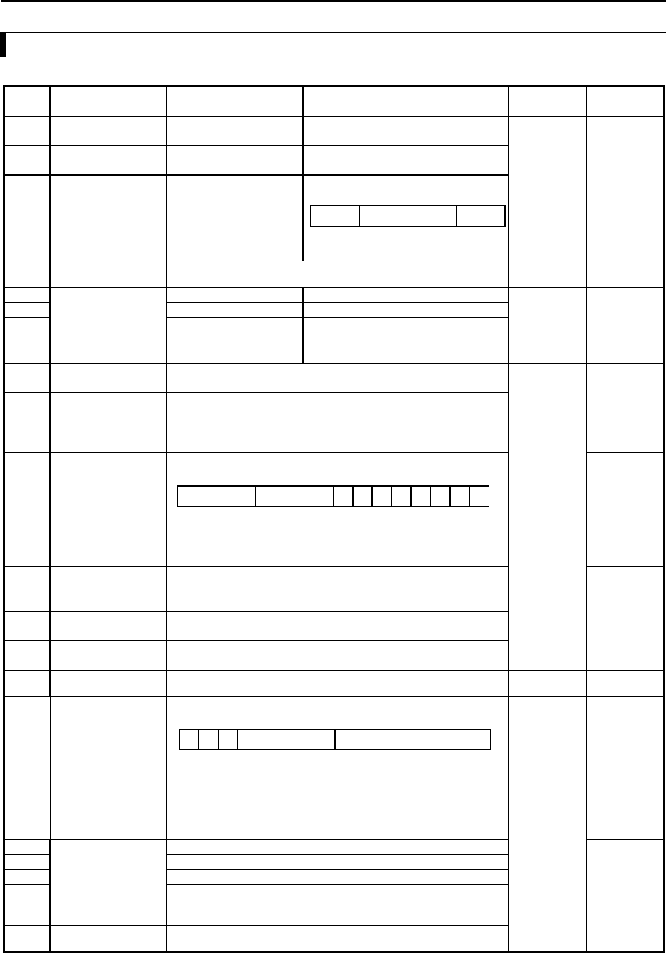
Chapter 12 Error Code List and Special Internal Outputs
12-9
12.5 Word Special Internal Output Area
The following lists the definitions of the word special internal output area (WRF000 to WRF1FF).
No. Name Storage data Description Setting
condition
Resetting
condition
WRF000 Self-diagnosis error
code
Error code
(Hexadecimal)
WRF001 Syntax/Assembler
error details
Syntax/Assembler error
code (Hexadecimal)
Error code for user program
Syntax/Assembler error is stored
WRF002 Further information
of I/O configuration
error
Mismatched slot number
a: Unit number (0 to 5)
b: Slot number (0 to F)
Set by the
system
Cleared by
user
WRF003
-F00A
Undefined Do not use.
WRF00B Year 4 digit year [yyyy]
WRF00C Month / date [mm dd]
WRF00D Day of the week Sunday: 0000 to Saturday: 0006
WRF00E Hour / minute [hh mm] (24-hour system)
WRF00F
Calendar and clock
present value
(4 digit BCD)
Seconds [00 ss]
Set by the
system
Always
displayed
WRF010 Scan time
(maximum value)
Max. scan time × 10 ms
WRF011 Scan time
(present value)
Current scan time × 10 ms
WRF012 Scan time
(minimum value)
Min. scan time × 10 ms.
(HFFFF at 1st scan)
Cleared by
the system (in
the RUN
starts)
WRF013 CPU status
a: CPU type (0011), b: Battery error (1=error, 0=no error),
c: Not used, d-g: Not used (Fixed to 0),
h: Halt (1=executing, 0=not executing),
i: CPU operation (1=RUN, 0=STOP)
Always
displayed
WRF014 Word internal output
capacity
Number of words for word internal output (WR) = H1000 Always
displayed
WRF015 Operation error code Operation error code
WRF016 Division remainder
register (low word)
Remainder data when division instruction executed
WRF017 Division remainder
register (high word)
Remainder data when division instruction executed
(Used only at double word operation)
Set by the
system
Cleared by
user
WRF018-
F019
Undefined Do not use.
WRF01A Setting of
Com. port 1
a: Transmission control procedures (0- Standard, 1-Simplified)
b-c: Not used
d: Baud rate during modem connection
= 00000: 4800 bps, = 00001: 9600 bps, = 00010: 19.2 kbps
= 00011: 38.4 kbps, = 00100: 57.6 kbps, = 00101: 2400 bps
= 4800 bps for other than the above
Set by user Cleared by
user
WRF01B Year 4 digit year [yyyy]
WRF01C Month / date [mm dd]
WRF01D Day of the week Sunday: 0000 to Saturday: 0006
WRF01E Hour / minute [hh mm] (24-hour system)
WRF01F
Reading or writing
register for calendar
and clock
(4 digit BCD)
Use with R7F8 or
R7F9 Seconds [00 ss]
Set by system
or user
Cleared by
user
WRF020
to F03B
Undefined Do not use.
15 12 11 8 7 4 3 0
0ab0
15 14 13 12 11 8 7 6 5 4 3 2 1 0
Unused a b c d e f g h i
15 14 13 12 8 7 0
a b c d Unused
Chapter 12 Error Code List and Special Internal Outputs
12-10
No. Name Storage data Description Setting
condition
Resetting
condition
WRF03C Port 1
Modem timeout time
a: Whether or not settings are present 0=No setting
1=Setting is present
Modem timeout time: 1 second increments (set with hexadecimal
value)
0=No timeout monitoring
Set by user Cleared by
user
WRF03D Port 2
Communication
settings
a: Setting bit 1=Set Set to 0 by the system after setting is
complete.
b: Transmission control procedures 0=Standard, 1=Simplified
c: Whether or not station numbers are present 0=No station
numbers, 1=Station numbers are present
d: Baud rate settings
= 00000: 4800 bps, = 00001: 9600 bps, = 00010: 19.2 kbps
= 00011: 38.4 kbps, = 4800 bps if other than the above
Station numbers: 2 digits from 00 through 31 of BCD
Set to 31 for values outside the range
Set by user Cleared by
user
WRF03E Potentiometer input 1 0 - 1023 Set by user Cleared by
user
WRF03F Potentiometer input 2 0 - 1023 Set by user Cleared by
user
WRF040
to F042
Occupied member
registration area 1
WRF043
to F045
Occupied member
registration area 2
WRF046
to F048
Occupied member
registration area 3
WRF049
to F04B
Occupied member
registration area 4
Occupied port number
a: 0=Not occupied, 1=Read-occupied, 2=Write-occupied
b: Loop number c: Unit number
d: Module number e: Port number
Set by the
system
Cleared by
the system
WRF04C
to F04F
Undefined Do not use.
WRF050 System ROM version System software version in internal ROM
WRF051 System ROM version System software version in external FLASH memory
Set by the
system -
WRF052 Undefined Do not use.
WRF053 Undefined Do not use.
WRF054 Power on timer Power on time [sec.] (low word)
WRF055 Power on timer Power on time [sec.] (high word)
Set by the
system -
WRF057 Detailed information
of counter setting
errors
a: Error in pulse frequency total
b: Pulse 4 frequency c: Pulse 3 frequency
d: Pulse 2 frequency e: Pulse 1 frequency
f: Counter 4 preset g: Counter 3 preset
h: Counter 2 preset i: Counter 1 preset
0=Normal, 1=Error
Set by the
system
Cleared by
the system
15 8 7 0
aNot used Modem timeout time
15 14 13 12 8 7 0
abc d Station number
15 8 7 0
aFixed to 0
bc
de
1514 876543210
aNot used bcdefghi
Chapter 12 Error Code List and Special Internal Outputs
12-11
No. Name Stored data Description Setting
condition
Resetting
condition
WRF057 Detailed information
of counter setting
errors
a: Error in pulse frequency total
b: Pulse 4 frequency c: Pulse 3 frequency
d: Pulse 2 frequency e: Pulse 1 frequency
f: Counter 4 preset g: Counter 3 preset
h: Counter 2 preset i: Counter 1 preset
0=Normal, 1=Error
Set by the
system
Cleared by
the system
WRF058 PI/O function
individual setting
request 1 *
a: Output number (during pulse setting)
Off-preset (during counter setting)
b: On-preset (during counter setting)
Frequency (during pulse setting), frequency, on-duty (during
PWM setting)
0=No changes, 1=Change request
Set by user Cleared by
the system
WRF059 PI/O function
individual setting
request 2 *
a: Output number (during pulse setting)
Off-preset (during counter setting)
b: On-preset (during counter setting)
Frequency (during pulse setting), frequency, on-duty (during
PWM setting)
0=No changes, 1=Change request
Set by user Cleared by
the system
WRF05A PI/O function
individual setting
request 3 *
a: Output number (during pulse setting)
Off-preset (during counter setting)
b: On-preset (during counter setting)
Frequency (during pulse setting), frequency, on-duty (during
PWM setting)
0=No changes, 1=Change request
Set by user Cleared by
the system
WRF05B PI/O function
individual setting
request 4 *
a: Output number (during pulse setting)
Off-preset (during counter setting)
b: On-preset (during counter setting)
Frequency (during pulse setting), frequency, on-duty (during
PWM setting)
0=No changes, 1=Change request
Set by user Cleared by
the system
WRF05D
to F06A
Undefined Do not use.
1514 876543210
aNot used bcdefghi
15 2 1 0
Not used ab
15 2 1 0
Not used ab
15 2 1 0
Not used ab
15 2 1 0
Not used ab
Chapter 12 Error Code List and Special Internal Outputs
12-12
No. Name Stored data Description Setting
condition
Resetting
condition
WRF06B Pulse and PWM
output auto
correction setting
01: For EH-***DTP
02: For EH-***DT
03: For EH-***DRP
04: For EH-***DRT
The output waveforms of the pulses and
PWM are automatically corrected by
setting the value corresponding to the
CPU model.
WRF06C Potentiometer CH1
WRF06D Potentiometer CH2
Sampling number: 0 to 40.
WRF06E Analog input type
selection
Selects whether the analog input is voltage or current.
a: Analog 1 selection 0=Voltage 1=Current
b: Analog 2 selection 0=Voltage 1=Current
WRF06F Counting mode of
2-phase counter
00: Mode 0 01: Mode 1
02: Mode 2 03: Mode 3
WRF070 I/O operation mode H00: Mode 0
H01: Mode 1
H02: Mode 2
H03: Mode 3
H10: Mode 10
WRF071 I/O detailed function
settings
I/O assignment for counter, PWM and pulse train output
WRF072
to F075
Output frequency,
On-preset value
Frequency setting value, on-preset setting value
WRF076
to F079
On-duty value,
Off-preset value
On-duty setting value, off-preset setting value
WRF07A
to F07D
Pre-load value,
Pulse output value
Counter pre-load value or pulse output value
WRF07E Input edge Counter input edge setting value
WRF07F Input filtering time Filter time ×0.5 ms, up to 40 (=20ms)
Set by user Cleared by
user
WRF080
to F19F
Undefined Do not use.
*: See Chapter 8 for more details.
15 14 13 0
ab Not used
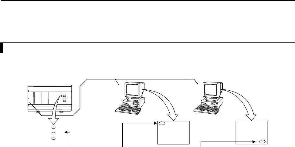
Chapter 13 Troubleshooting
13-1
Chapter 13 Troubleshooting
13.1 Error Display and Actions
The display locations of errors detected by individual device in the MICRO-EH system are shown in Figure 13.1. When
an error occurs, take an action according to the error code list.
OK
POW
RUN
LADDER EDITOR
for Windows®
LADDER EDITOR
OK Lamp L/E for Windows® error display
L/E error display
Figure 13.1 Error display locations of the MICRO-EH
(1) Error display
(a) Error display on the main unit
The MICRO-EH will perform self-diagnostic tests using the microcomputer, and when there is an error the contents
are indicated in the combination of lit/flashing/not lit of the OK and RUN lamps located in the front of the main unit.
See the error code list and action in Chapter 12, for the detailed error codes and actions.
(b) Programmer error display
Error codes encountered during program device operation, such as duplicate definition error, undefined error,
operation error, program over, etc., will be displayed on the programming device. For detailed error codes,
refer to the error code list in the programming device manual.
(c) GPCL error display
The error detected by the CPU during the GPCL operation is displayed at the bottom left of the screen. For
the details of error codes, see the list of error codes in the GPCL manual.
(d) Setting in the special internal output
An error code is set in the special internal output area (such as WRF000). The smaller the error code value,
the more serious the error is. When two or more errors occur, the smaller number is set. For example, if “71”
(battery error) and “31” (user memory error) occur simultaneously, “31” is set. If the levels are the same, the
cause code generated last will be displayed.
The clearing of error special internal output is performed by setting the special internal output R7EC to “1.”
The R7EC can be set to “1” either by connecting the programming device or by including a subprogram that
sets the R7EC using external input within the program. (If turning R7EC on by the program, always set it on
after the error cause has been verified. However, if R7EC is turned on by a program that would generate a
congestion error, the system may clear the error cause and rerun after detecting a congestion error.)
Note: Error codes are set in hexadecimal values. Verify error codes by setting the monitor to hexadecimal
display.

Chapter 13 Troubleshooting
13-2
The following shows the range of the special internal output that is cleared when R7EC is set to “1.”
No. Bit special internal output No. Word special internal output
R7C8 Fatal error flag WRF000 Self-diagnostic error code
9 Microcomputer error 1 Syntax/assembler error details
A User memory error 2 I/O verify mismatch details
B (Undefined)
C Memory size over
D I/O verify mismatch
E (Undefined)
R7CF (Undefined)
R7D0 (Undefined)
1 Congestion error (normal scan)
2 Congestion error (periodical scan)
3 Congestion error (interrupt scan)
4 Syntax/assembler error
5 (Undefined)
6 (Undefined)
7 (Undefined)
8 (Undefined)
9 Battery error
A (Undefined)
R7DB Self-diagnostic error
When all of the special internal output data cannot be cleared during program execution, refer to the self-
diagnostic error code list and clear only the corresponding error flags by using forced set of the programmer
or peripheral unit.
Caution
If the internal output for a self-diagnostic error R7DB (WRF000) is used as a system error for the stop condition of CPU
RUN, the R7DB may be turned on even with an error of the warning level (battery error, etc.), causing the CPU to stop.
Therefore, do not use the internal output of the self-diagnostic error as a condition for stopping the CPU.
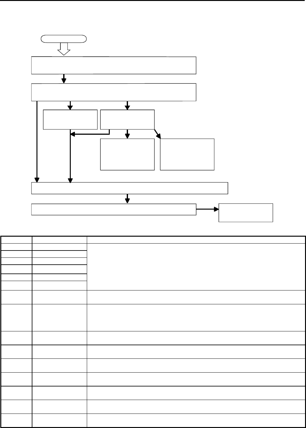
Chapter 13 Troubleshooting
13-3
(2) Corrective actions when an error occurred
The process flow when an error occurred is shown below.
Error occurred
Reference the bit special
internal output (14-1).
Reference the word
special internal output
(14-2).
Reference the grammar/
assemble error (WRF001)
detailed data (13-2) and
remove the error cause.
Reference the operation
error (WRF015) detailed
data (13-3) and remove
the error cause.
Remove the error cause according to the corrective action for each error code as shown below.
Contact our service
department.
If there are spare parts available, replace the parts.
Error is detected by the CPU module and displayed by lit/flashing/not lit
of RUN and OK LEDs.
Verify the self-diagnostic error code (WRF000) with the RUN and OK
LED statuses or using a peripheral unitand refer to error code list.
Error code Error name Corrective action
11 System ROM error
12 System RAM error
13 Microcomputer error
1F System program error
23 Undefined instruction
27 Data memory error
Restart the power.
If the same error occurs, it is a hardware error in the CPU module, so replace the CPU module
with a spare.
Make sure that there are no machines, etc. that generate excessive noise near MCRO-EH.
Note: The 1x error cannot be verified since peripheral units cannot be connected until the
system starts up after powering on again.
Power shut-off, power
supply error
Check the power supply voltage of the basic unit and expansion unit.
31 User memory error The contents of the user program is destroyed. Perform initialization and transfer the program
again.
This is displayed when the machine is stored with a worn-out battery or without battery for a
long period of time.
33 User memory size
error
This may be displayed when the contents of the memory within the basic unit is unstable.
If the same error occurs after initialization, replace the basic unit with a new one.
34 Syntax/assembler
error
There is a syntax/assembler error in the user program.
Verify the program and I/O assignment.
41 I/O information
verification error
Check the I/O assignment.
Check the expansion cable connection.
44 Congestion error
(normal scan)
Change the program so that the scan time of the user program is less or change the congestion
check time.
45 Congestion error
(periodic scan)
Change the program so that the periodic interrupt program execution time is less.
46 Congestion error
(interrupt scan)
Perform interlock externally to that the same interrupt will not occur during interrupt
processing. Change the program so that the execution time of the interrupt program is short.
5F Backup memory error There is a possibility that the FLASH memory cannot be written to. Reset the power after the
user program is read and saved to the peripheral units.
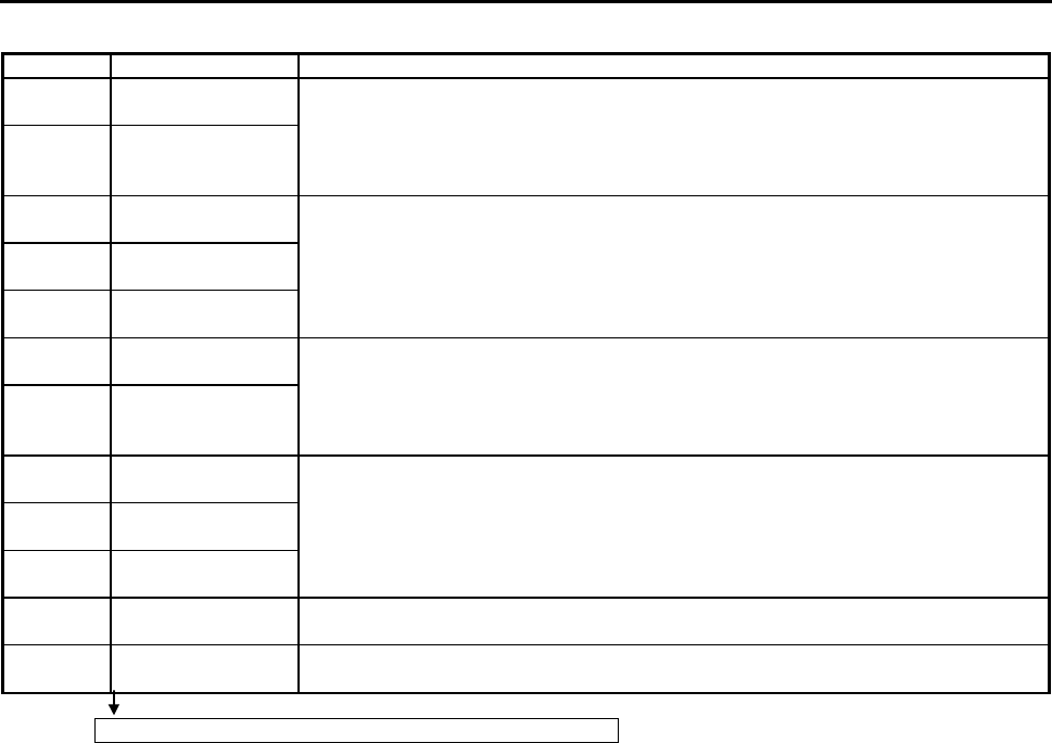
Chapter 13 Troubleshooting
13-4
Error code Error name Corrective action
61 Port 1 transmission
error (parity)
62 Port 1 transmission
error
(framing/overrun)
Check the connection of the connector cable.
Check the settings such as the transmission speed.
Check to see if there are any sources of noise near the cable.
63 Port 1 transmission
error (timeout)
64 Port 1 transmission
error (protocol error)
65 Port 1 transmission
error (BCC error)
Check the connection of the connector cable.
Check to see if there are any sources of noise near the cable.
Verify the protocol specification, examine the host computer processing and correct any
errors.
67 Port 2 transmission
error (parity)
68 Port 2 transmission
error
(framing/overrun)
Check the connection of the connector cable.
Check the settings such as the transmission speed.
Check to see if there are any sources of noise near the cable.
69 Port 2 transmission
error (timeout)
6A Port 2 transmission
error (protocol error)
6B Port 2 transmission
error (BCC error)
Check the connection of the connector cable.
Check to see if there are any sources of noise near the cable.
Verify the protocol specification, examine the host computer processing and correct any
errors.
71 Battery error Replace the battery with a new one.
Verify the connection of the battery connector.
91 Port 1
Modem no response
Verify the connection with battery.
Replace the modem with a new one.
Perform the following procedures to erase the error display.
(a) When the basic unit is being stopped
Turn the basic unit RUN switch (or RUN terminal) to “STOP,” then to “RUN” again.
If the cause of the error has been corrected, the OK lamp is lit. However, the error information remains in the
error special internal output, which stores the CPU error types and details. (This makes it possible to analyze
the error after recovery.) To reset the error information, perform the procedures shown in (b) or turn ON the
special internal output (R7EB) of the power failure memory clear on the peripheral units.
(b) When the CPU is still running (RUN)
Set the special internal output R7EC to “1” to clear the OK lamp indicator and the error internal output.

Chapter 13 Troubleshooting
13-5
13.2 Checklist when Abnormality Occurred
If an error occurs in the MICRO-EH system, check the following items. If there are no problems in the following items,
contact our service department.
(a) Power supply related items
•Is the power voltage correct? (85 to 264 V AC)
•Are there any warps in the power supply waveform?
•Are there any excessive noises in the power supply?
•Is power supplied for all basic and expansion units?
(b) CPU related items
•Are the initial settings (CPU initialization, I/O assignment, parameter settings, etc.) proper?
•Are there any error codes that are output to the special internal output?
•Is the RUN switch (or RUN terminal) in the proper location?
•Are batteries mounted properly? Is the battery life still remaining? (23/28-point types only)
(c) Input module related items
•Is the input voltage within the specifications for the internal section?
•Is there any noise or chattering in the input?
•Do the I/O assignment numbers in the program match?
•Is the wiring done properly?
(d) Output module related items
•Do the module and the load power supply type (DC/AC) match?
•Do the load voltage and current match the specification of the output section?
•Is there any noise or chattering in the output waveform?
•Is the wiring done properly?
•Do the I/O assignment numbers in the program match?
•Are there any unintentional overlaps in the output numbers?
(e) Wiring related items
•Is the wiring between the expansions mixed up with other wires?
•Are the power supply wiring and I/O cables separated?
•Are there any foreign substances in the connector of the basic/expansion units?
Cautions
(a) When returning the unit for repair, please notify us of the malfunctioning conditions in as much detail as possible
(including error codes, malfunctioning I/O bit number, will not turn on or off, etc.).
(b) The tools and devices necessary for troubleshooting are briefly as follows:
Phillips/flathead drivers, digital multimeter, tester, oscilloscope (necessary depending on the case) etc.
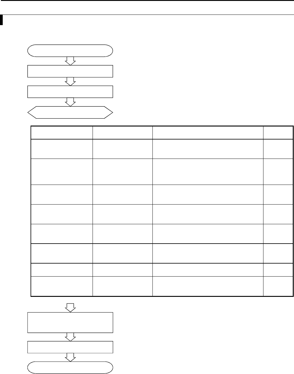
Chapter 13 Troubleshooting
13-6
13.3 Procedures to Solve Abnormality
The following shows the processing flow when a problem has occurred:
Problem occurred
Bring the system to a safe condition
Record the status
Problem, Analysis, Presumption
Major problems Verification points Typical causes of problem Reference
item
PLC will not start Power LED, CPU error
code
Power supply problem, power shut-off,
insufficient power supply capacity, fatal CPU
error
(a)
Will not operate
(will not RUN)
CPU error code, CPU
LED, Internal output of
error
I/O assignment problem, incorrect parameter
settings, incorrect user program, syntax error,
operating conditions not established, write-
occupied status
(b)
Operation stopped
(RUN stopped)
Power LED, CPU LED,
CPU error code
Power supply problem, expansion power supply
problem/shut-off, CPU problem, memory
problem
(c)
Erroneous input, no input
(abnormal operation)
CPU LED, I/O LED
Monitoring by peripheral
units
User program timings, input power supply, bad
connection, problem in input area, I/O inductive
noise
(d)
Counter input does not
operate
Input LED, special
internal output setting
Input power supply, bad connection, problem in
input area, I/O inductive noise, operating mode
setting error
(e)
Output error, no output
(abnormal operation)
CPU LED, I/O LED,
Monitoring by peripheral
units, Forced setting
User programming, bad connection, problem in
output area, I/O inductive noise
(f)
PWM pulse output does
not operate
Output LED, special
internal output setting
Bad connection, problem in output area, I/O
inductive noise, operating mode setting error
(g)
Peripheral unit problem CPU error code, fuse,
peripheral units
Fatal CPU error, peripheral unit problem,
peripheral unit setting error, cable problem,
broken fuse
(h)
Verify the system operation
Correct or replace the faulty area
(Verify according to the item
corresponding to the problem.)
Operation
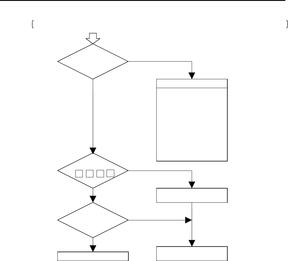
Chapter 13 Troubleshooting
13-7
(a) PLC will not start
The CPU OK LED does not turn off even when power is started, nor peripheral units cannot be connected on-line.
Power supply check
AC power supply type
•AC power supply voltage (at
the input terminal)
•DC power supply voltage (at
the output terminal)
DC power supply type
•DC power supply voltage (at
the input terminal)
•DC power supply voltage (at
the output terminal)
Fitting between terminal stand
and main unit
YES
YES
NO
NO
NO
YES
131211
Contact our service department
Malfunction due to noise
There is a possibility of power
supply area damage
Occur frequently?
1F
POWER LED is lit
Fatal CPU error
Self-diagnostic error code
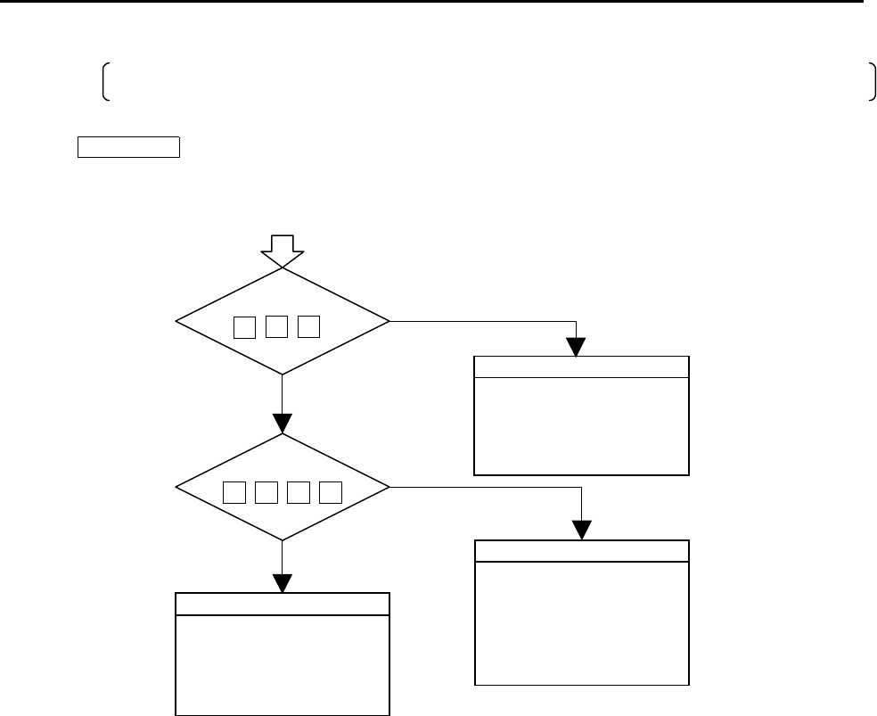
Chapter 13 Troubleshooting
13-8
(b) Will not operate (will not run)
Even if the PLC operation conditions are met, the CPU does not operate (the RUN LED does not turn on) and
remains stopped. However, the peripheral units go on-line.
Caution
If the CPU is WRITE-occupied, the CPU will not run even if the RUN switch is switched from “STOP” to “RUN.” The
CPU starts running by pressing the GRS key after peripheral units are connected.
Check the memory
Perform CPU initialization
Set memory parameters
Reset the power
Replace CPU if above steps
does not remedy the problem
NO
YES
YES
NO
Serious user program error
45443423
Self-diagnostic error code
Serious memory error
3331
Self-diagnostic error code
Check the user program
•Check programs using
peripheral devices
•Error special internal output
monitor
•Verify scan time
•Correct program
Check I/O assignments
•Check the assignment table at
peripheral devices
•Can I/O assignment be
corrected?
•Malfunction due to noise
27
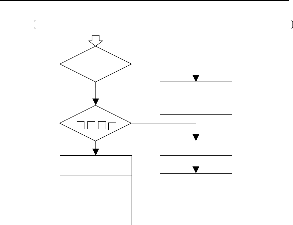
Chapter 13 Troubleshooting
13-9
(c) Operation stopped (RUN stopped)
During normal operation, the CPU suddenly stops (the RUN LED turns off).
NO
YES
NO
YES
131211 1F
Check the power supply
•Instantaneous power failure
occurs
•Power is shut off on the
expansion unit side
Contact our service department
if a fatal error occurs frequently
Turn the power off and turn it
back on
Check the program
Check parameters
Check I/O assignment
•Parameter settings
•Program congestion
•Check I/O assignment
•Duplicate use of the timer
counter
•Retransfer of program
•Connection with the expansion
connector
POWER LED is lit
(Power supply is
normal)
Fatal CPU error
Self-diagnostic error code
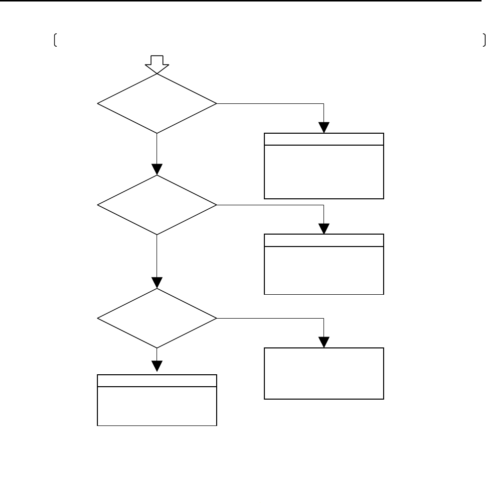
Chapter 13 Troubleshooting
13-10
(d) Wrong input at input module or no input (operation problem)
The CPU runs, but the input data is not correct.
Check input signals
•Input signal voltage
•Input power supply type
•Cable disconnection
•High-speed pulse is entered
in a normal input
NO
YES
YES
NO
Check input signals
•Check input monitor
•I/O assignment
•Program
•Input signal voltage
NO
YES
LED error
∗LED replacement may not be
performed by the user, so a
repair request must be
submitted.
Check for input error
•Check input signal source
•Check input program
•Malfunction due to noise
Input LED is not lit
Input is not read
Input LED is lit
Input is not read
Input LED is not lit
Input is read
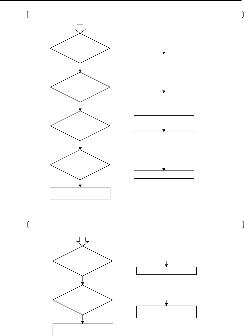
Chapter 13 Troubleshooting
13-11
Data cannot be entered.
I/O assignment error is generated, but data is read.
NO
YES
YES
NO
YES
NO
NO
YES
Is there a wiring
error, disconnection
or loose screw on the
terminal block?
Replace the terminal block
Contact our service department
Contact our service department
Perform rewiring
Check the wiring systems
Change the voltage to satisfy
the specifications
Is there input
when the voltage is
checked between
the common and bit
on the input side?
Is the LED lit?
Is there an error on the
internal contactors on the
terminal stand?
YES
NO
YES
NO
Are the program and I/O
assignment correct?
Replace the expansion cable
Correct the error
Replace the expansion unit
Is the cable in the
expansion unit
damaged?
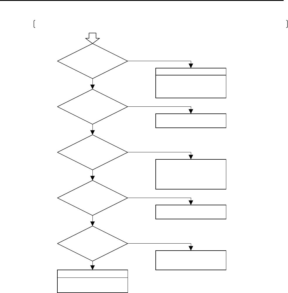
Chapter 13 Troubleshooting
13-12
(e) The counter input does not function
The CPU operates, but the input data is incorrect
Set the operating mode for the
peripheral devices
Note: The operating mode can
only be changed while the
CPU is bein
g
sto
pp
ed
Set the I/O functions on devices
such as peripheral devices
Turn on the setting enabling
request flag ON using peripheral
devices
•Check the input pulse
•Malfunction due to noise
YES
NO
YES
NO
YES
NO
YES
NO
Set the pulse input to 5kHz or
less
NO
YES
Check the in
p
ut area
Check the input area
•Check the input signal source
•Malfunction due to noise
•Cable is disconnected
Does it operate as
normal input?
Are the operating mode
settings correct?
Are the various
settings valid?
Are the I/O function
settings correct?
Are pulses that exceed
5 kHz being input?
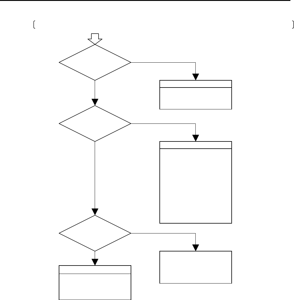
Chapter 13 Troubleshooting
13-13
(f) Wrong output from output module or output module will not output (operation problem)
The CPU operates, but output signals are not correct.
Check the output area
•Forced output
•I/O assignment
•Program
NO
YES
YES
NO
Check output signals
•Output signal voltage
•Power supply voltage for load
•Terminal block wiring
•Terminal block connector
connection
•Voltage between the common
and the bit
•Wiring
Especially for the S terminal
on the transistor
•The drive power supply for the
relay is not connected
NO
YES
LED error
∗LED replacement may not be
performed by the user, so a
repair request must be
submitted
Check for output error
•Check the output power
supply
•Check the output program
•Malfunction due to noise
Output LED is not lit
Will not output
Output LED is lit
Will not output
Output LED is not lit
Will output
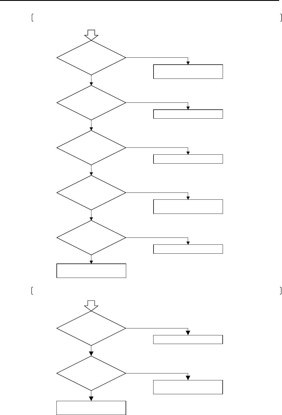
Chapter 13 Troubleshooting
13-14
The CPU operates, but output signals are not detected.
I/O assignment error occurred, but output is normal.
Replace the expansion cable
Correct the error
YES
NO
Replace the expansion unit
NO
YES
Are the program and
I/O assignment
correct?
Is the expansion unit
cable damaged?
YES
NO
NO
YES
YES
YES
NO
NO
YES
NO
Is there a wiring error,
disconnection or loose
screw on the terminal
block?
Replace the terminal block
Supply 24 VDC power
Contact our service department
Check the program
Perform rewiring
Is the voltage satisfying
the specification in the
terminal block? Is the
polarity correct?
Is the LED lit?
Are there any problem in
internal contactors of the
terminal block?
Is the relay drive power
supply connected?
Change the voltage and polarity
to satisfy the specifications
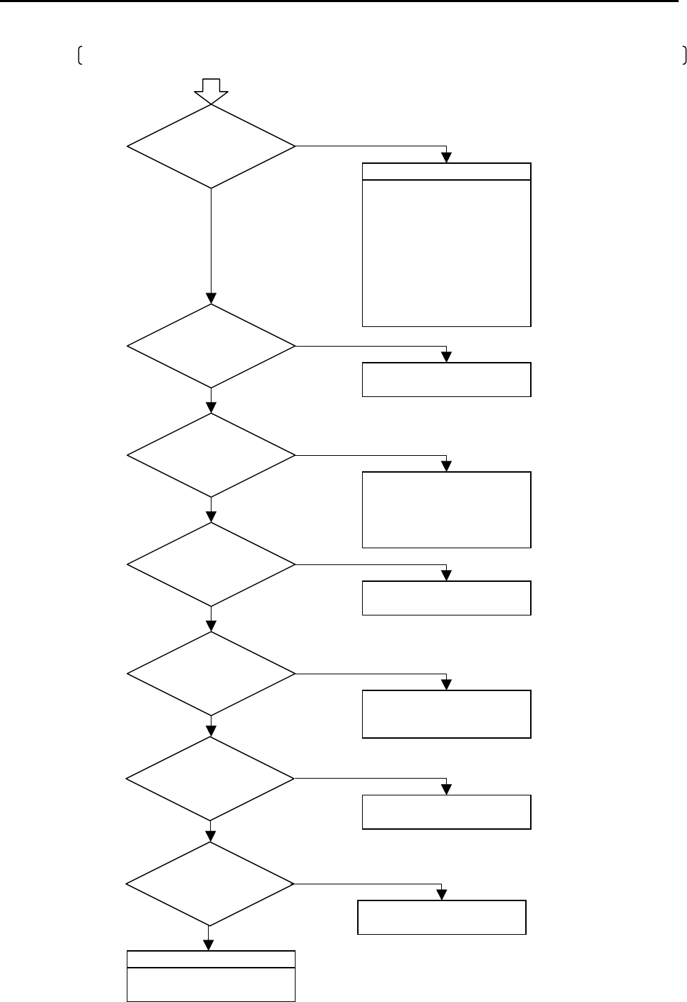
Chapter 13 Troubleshooting
13-15
(g) The PWM and pulse output does not operate
The CPU operates, but the pulse output and PWM output are not correct
*Pulse output only. 2 kHz is the upper
limit for PWM output.
Turn on the setting enabling
request flag ON using
peripheral devices
YES
NO
Set the operating mode for the
peripheral devices
Note:The operating mode can
only be changed while the
CPU is being stopped
Set the I/O functions on devices
such as peripheral devices
YES
NO
YES
NO
Set the pulse input to be a total
of 5 kHz or less*
NO
YES
Check the output area
YES
NO
Check the output area
NO
YES
The expected pulse output from
the relay is not output
•Output signal voltage
•Power supply voltage for the
load
•Terminal stand wiring
•Terminal stand connection
•Voltage between the
common and bit
•Wiring
Especially for the S terminal on
the transistor
• Check the output power supply
• Malfunction due to noise
Are the various
settings valid?
Are the operating mode
settings correct?
Are the I/O function
settings correct?
The total pulse output
exceeds 5kHz?
Does it operate as
normal output?
Pulse is output using
the relay output
YES
Wait until the write to the
backup memory is completed.
*1 Pulse output only.
Is the backup
memory being
written? *1
NO
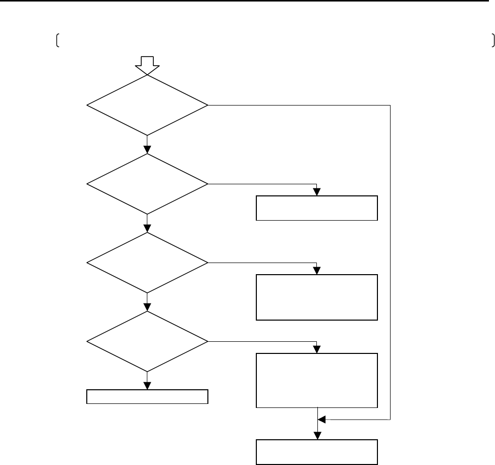
Chapter 13 Troubleshooting
13-16
(h) Peripheral units problem
Peripheral units cannot be connected.
Replace the connection cable
Please contact our service
department.
NO
YES
Expansion connector check
Expansion cable check
YES
NO
YES
NO
YES
NO
Correct the setting
Set the CPU DIP SW to the
communication speed of the
peripheral unitused
Broken fuse
∗Fuse replacement may not be
performed by the user, so a
replacement request must be
submitted
Is it a fatal CPU error?
Are the connection
cable type, continuity
and connector
connections normal?
Are the CPU
communication setting
correct?
Is there 5 V DC output
when a 5 V DC power
supply is required?
Chapter 14 Operation Examples
14-1
Chapter 14 Operation Examples
To understand the basic operation of the MICRO-EH, this chapter explains samples of operations such as inputting
simple programs and verifying operations.
The following programming devices can be used:
Peripheral unit name Form
1 H series ladder diagram
instruction language software
LADDER EDITOR
HL-PC3
HL-AT3E
2 H series ladder diagram
instruction language software
LADDER EDITOR for Windows® version
HLW-PC3
HLW-PC3E
* Graphic input device (format: GPCL01H) can be used except on-direct mode.
(1) Operation verification procedures
An operation is verified according to the following procedures:
STEP 1
STEP 2
STEP 3
STEP 4
STEP 5
STEP 6
STEP 7
End
Start
Start the LADDER EDITOR for Windows®
Perform initial settings
Input program
Check program errors
Save program
Transfer program to the CPU
Monitor (verify the operation)
A personal computer and LADDER EDITOR for Windows® are used as the peripheral units in the example. For
details, refer to the user's manual for each peripheral unit.
(2) Detailed operation example
The following explains an operation example using the module and sample program from step 1.
CPU: 14-point type
Slot 0: Bit point X48
Slot 1: Bit point Y32
Slot 2: 16 vacant points
Input/output operating mode: Mode 0
(WRF070 = 0, default value)
Operation of program
Turn Y100 and Y 102 on and
Y101 and Y103 off and vice
versa, alternating at one second
intervals.
R7E3
R0 = 1
TD0 Y100 = 1
Y101 = 0
Y102 = 1
Y103 = 0
R0
(00001)
(
00002
)
. 1S 10
TD0
(00003)
TD0 Y100 = 0
Y101 = 1
Y102 = 0
Y103 = 1
TD0 TD1
(00005)
TD1
(00004)
. 1S 10
Chapter 14 Operation Examples
14-2
S T E P 1 Starting the LADDER EDITOR for Windows®
1. Start the personal computer.
Start the personal computer.
2. Start the LADDER EDITOR for Windows® system (GRS screen).
From the Start menu of Windows®, click
[Program] → [Hladder] → [Hladder].
As LADDER EDITOR for Windows® is started,
the GRS screen is displayed.
Startu
p
3. Switching to Offline mode.
Click [Offline] in the Menu bar.
GRS screen
The Read/Edit screen is displayed.
Mode switchin
g
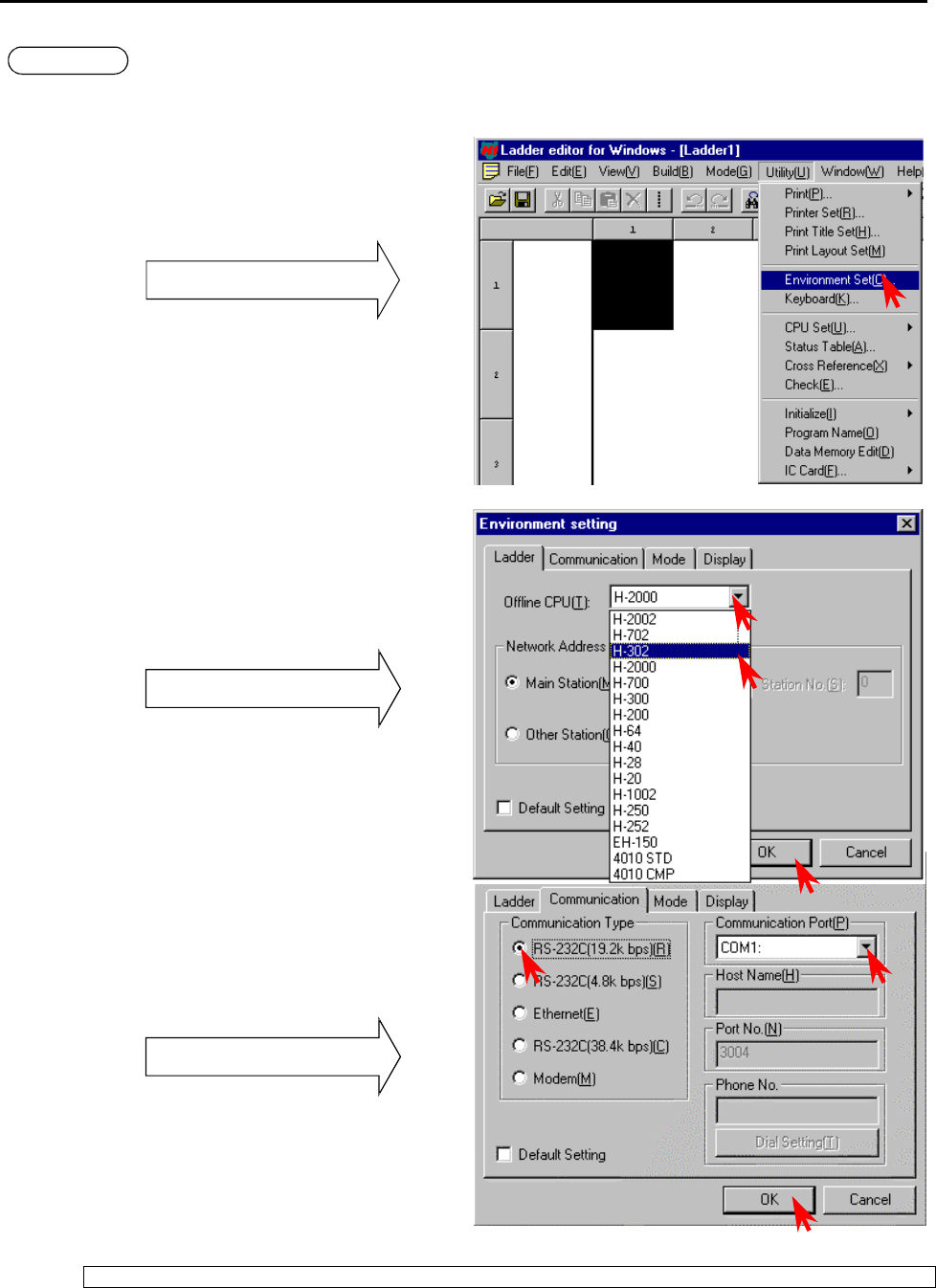
Chapter 14 Operation Examples
14-3
S T E P 2 Initialization
Settings for the CPU type, memory type and I/O assignment are performed.
1. Setting the CPU type
Click [Utility] → [Environment Settings] in
the Menu bar.
Pull-down menu
The Environment Setting dialogue box is displayed.
Specify the CPU type from the Ladder tag.
•Click the W of the Offline CPU field to show the
available CPU types in the pull-down display.
Select the CPU type.
•Click the [OK] button.
Pull-down display of CPU types
Specify the transmission speed from the
Communication tag.
•Select the transmission speed set with the DIP
switches of the MICRO-EH main unit (in case of
the 10-point type CPU, the transmission speed is
fixed at 4800 bps).
• Specify the communication port.
• Click the [OK] button.
Pull-down display of CPU types
Select “H-302” for the CPU type setting.
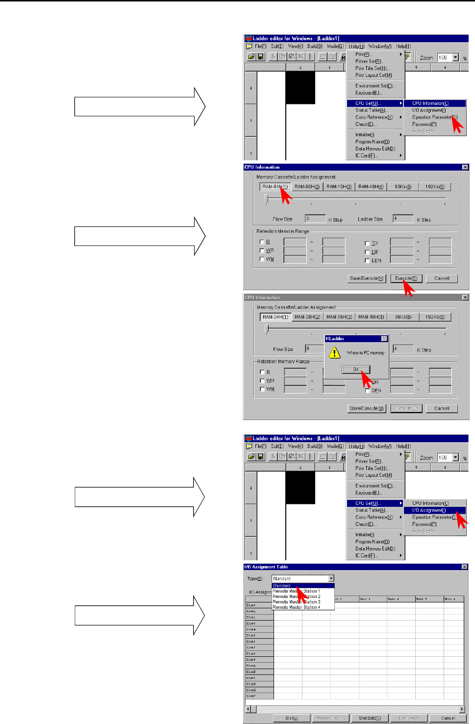
Chapter 14 Operation Examples
14-4
2. Setting the memory type
Click [Utility] → [CPU Setting] → [CPU
Information] in the Menu bar.
The CPU Information dialogue box is displayed.
Pull-down menu
•Click the Memory Cassette/Ladder Assign button
and select the memory cassette size.
•Click [Execute] or the [Memory/Execute]
button.
CPU Information dialogue box
•Click the [OK] button in the confirmation
dialogue box.
Set the memory cassette size to RAM-04H.
[Execute]: Save to the PC memory
[Memory/Execute]: Save to the PC memory and
Window registry.
3. Assigning I/O
Click [Utility] → [CPU Setting] → [I/O
Assign] in the Menu bar.
Pull-down menu
The I/O Assign List dialogue box is displayed.
Click the W of the Types field and select
[Standard] from the pull-down display.
I/O Assign List dialogue box
There are two setting methods for the subsequent
procedures.
•From the I/O Assign List
•From the I/O Assign List → Slot Setting Status
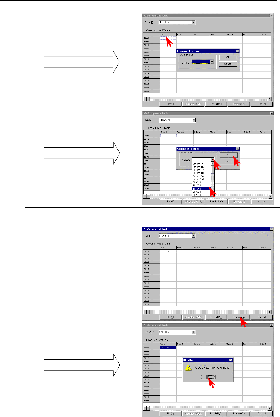
Chapter 14 Operation Examples
14-5
[Setting from the I/O Assign List]
1] Double-click the cell for the unit number and
slot number to be set.
The Assignment Setting dialogue box is displayed.
The Assignment Setting dialogue box
v
2] Click the W of the data and select I/O type
from the pull-down display.
3] Click the [OK] button to close the Assignment
Setting dialogue box.
Setting of I/O type
In the same way, repeat steps 1] to 3] to assign X48
and 16 vacant points to Slot 1 and 2 respectively.
If a wrong value has been entered, the slot is left blank by assigning [Vacant 0] and is treated as though nothing is
assigned to it.
4] Click the [Execute] button.
The information assigned to the PC memory is
written.
5] Click the [OK] button in the confirmation
dialogue box to close the I/O Assignment List
dialogue box.
Confirmation dialogue box
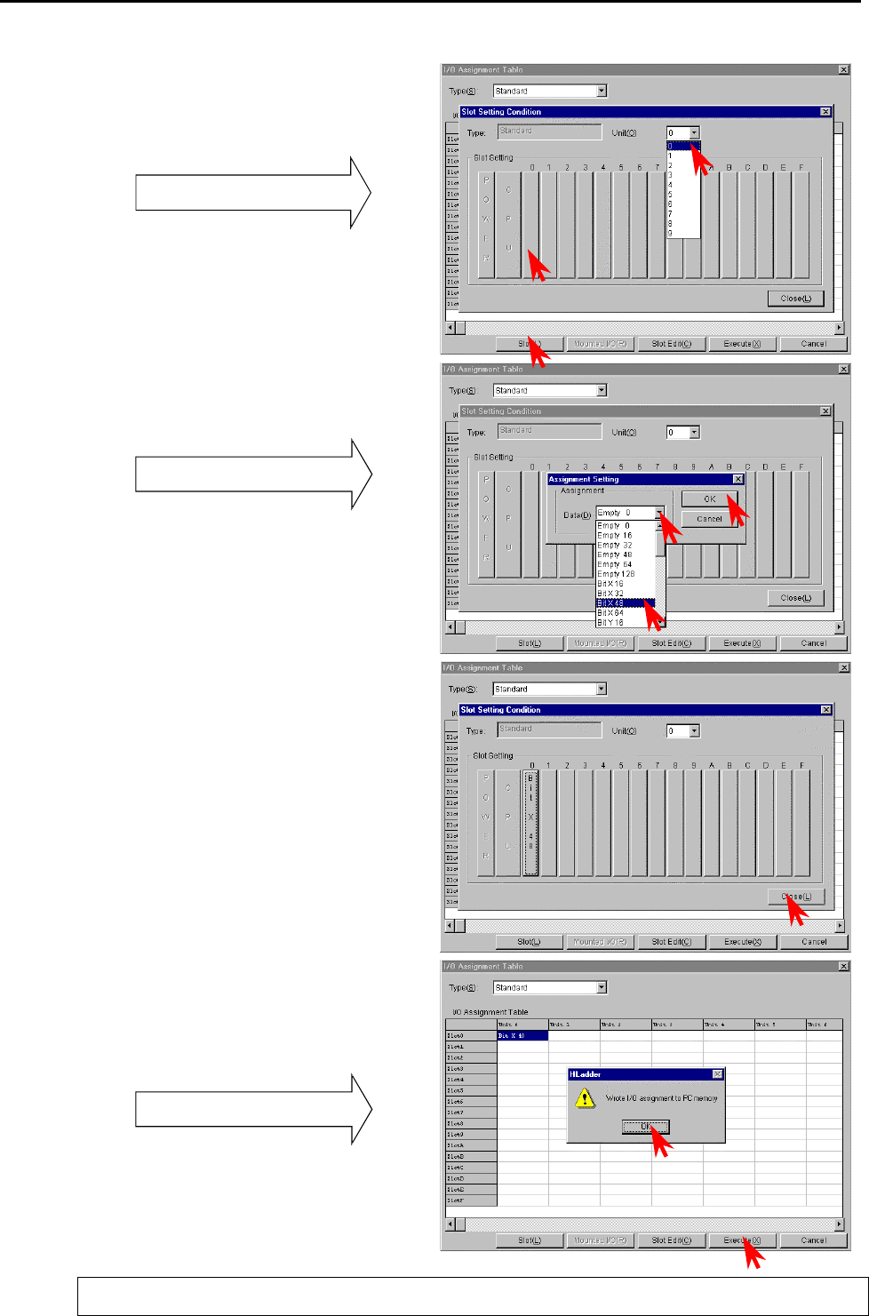
Chapter 14 Operation Examples
14-6
[Setting from the Slot Setting Status]
Click the [Slot] button to display the Slot Setting
Status dialogue box.
1] Click the W of the unit and select the unit
number from the pull-down display.
2] Click the button of the slot number to be set.
Slot Setting Status dialogue box
3] Click the W of the data and select the I/O type
from the pull-down display.
4] Click the [OK] button and close the
Assignment Setting dialogue box.
Specification of I/O type
In the same way, repeat the steps 1] and 2] to 4] to
set other unit and slot numbers in order to perform
I/O assignment according to the unit to be used.
In this example, X48 and 16 vacant points are
assigned to slots 1 and 2 respectively.
5] Click the [Close] button to close the Slot
Setting Status dialogue box.
Enter the I/O assignment set in the Slot Setting
Status into the I/O Assignment List.
6] Click the [Execute] button to write the
assigned information to the PC memory.
7] Click the [OK] button in the confirmation
dialogue box to close the I/O Assignment List
dialogue box.
Confirmation dialogue box
For online mode, it is possible to read the I/O mounted on the CPU by the “Mount” button. For details, refer to the
“Reading Mounted I/O” of the programming device.
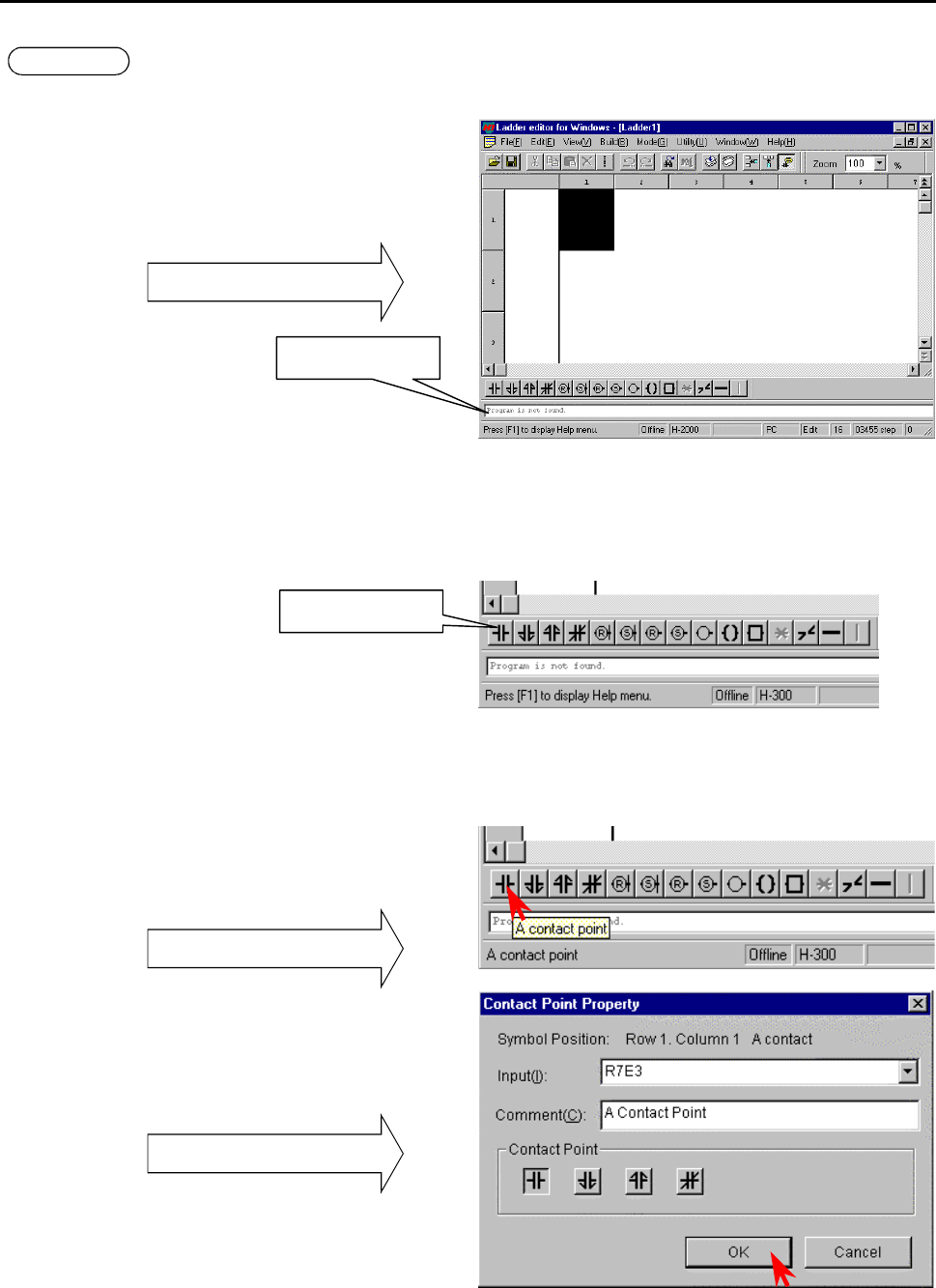
Chapter 14 Operation Examples
14-7
S T E P 3 Program Input
1. Input a program.
At first, the output window displays “there is no
program” in the bottom left of the Read/Edit
screen.
The cursor , which indicates the program input
position, is placed at the top left of the screen.
Read/Edit screen
[Input procedure of ladder program]
Repeat steps 1] to 4] to proceed with symbol input. The usual operations found in other Windows applications, such as
cut, copy, paste, and move, can be performed on already input symbols.
1] Specify the input position. (Move the cursor by clicking the mouse or the arrow keys.)
2] Click symbols in the Symbol bar.
3] Input the desired function (I/O, comparison expression, arithmetic expression) in the dialogue box for the symbol
displayed.
4] Click the [OK] button in the dialogue box.
[Example of entering a contact]
1] Begin from the cursor position at the top left.
2] Click the symbol for contact A.
The dialogue box for contacts is displayed.
Symbol selection
3] Enter “R7E3” as the I/O No. in the Input field.
(I/O No. (half-width alpha-numeric input) can
be entered by the keyboard only, or by
selecting the initial letter(s) from the pull-down
menu of W and by typing the rest.)
Enter a proper comment.
Contact property
4] Click the [OK] button.
The dialogue closes.
Output window
Symbol bar
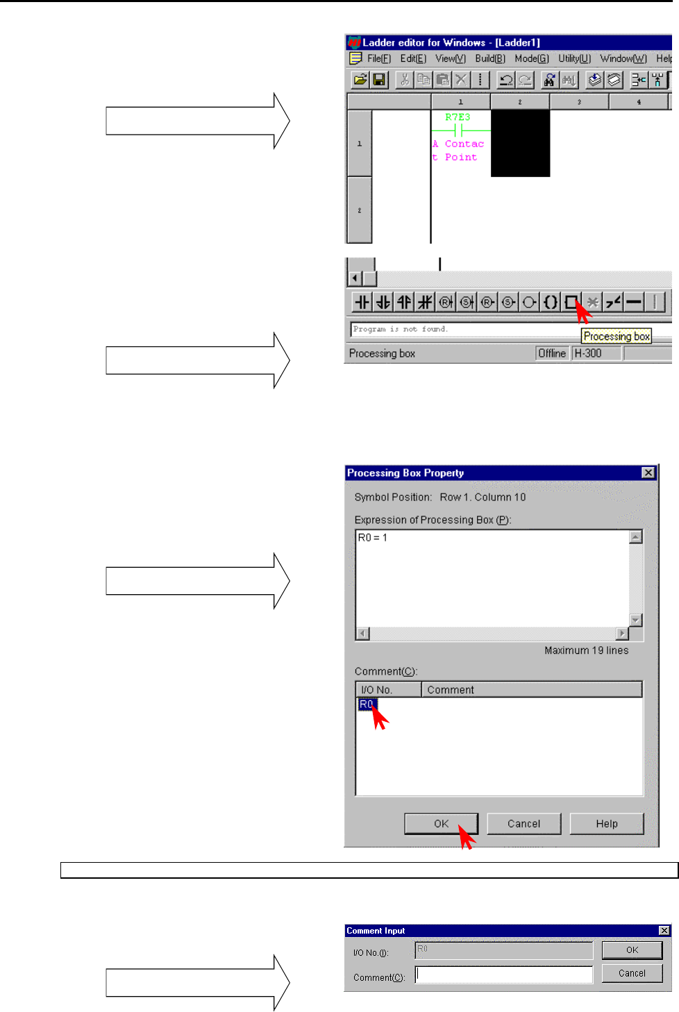
Chapter 14 Operation Examples
14-8
When the dialogue box closes, the symbol is
displayed in the Read/Edit screen and the cursor
shifts.
Display of symbol
The comment is displayed under the symbol.
[Example of entering a Processing Box]
1] The specification of the input position can be
omitted when entering symbols into the same
circuit as the contact above.
2] Click the symbol for Processing Box.
Symbol selection
The cursor moves to the far-right portion of the
screen automatically.
The dialogue box for the processing box symbol is
displayed.
3] Input arithmetic expressions in the Expression
in Processing Box text field.
Multiple lines (a maximum of 19) can be input by
including line breaks
Processing Box properties
The comment for the I/O No. written to the
Processing Box is displayed by clicking the
Comment column.
If there are no comments, only the I/O No. is
displayed.
Always enter a space before and after “=“.
•The Comment Input dialogue box is displayed by
double-clicking the I/O No. displayed in the
Comment column.
•Input a comment and click the [OK] button.
Comment Input dialogue box
4] Click the [OK] button in the Processing Box.
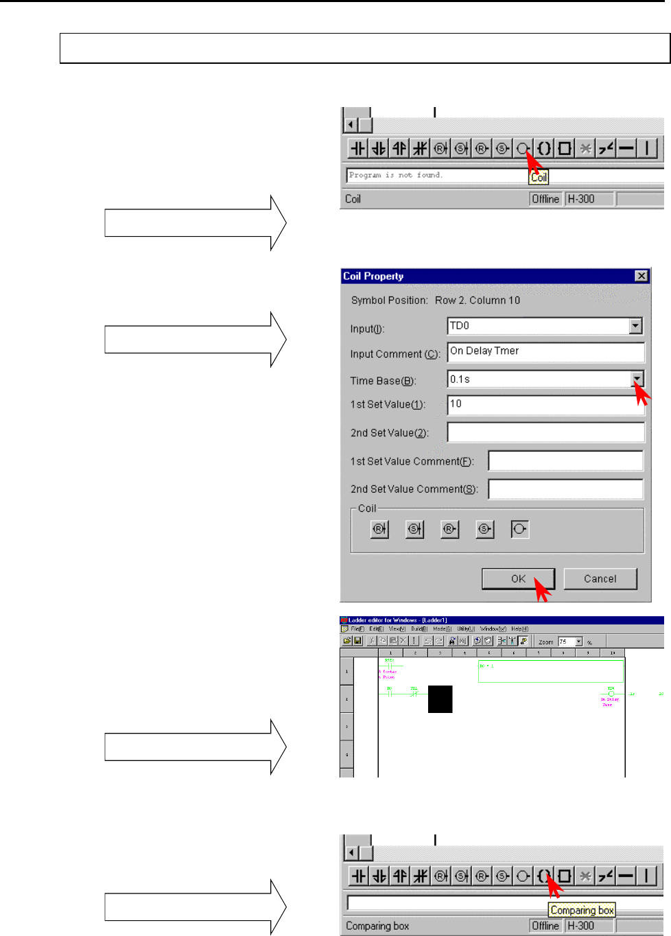
Chapter 14 Operation Examples
14-9
The input of the horizontal line symbol, which connects between symbols, may be omitted. (Symbols are connected by
horizontal lines by the automatic wiring function at circuit write.)
[Example of entering a timer]
1] Specify the input position, or omit the
specification if entering it in the same circuit.
2] Click the symbol for coil.
When the specification of the input position is
omitted, the cursor automatically moves to the
far-right portion of the screen.
Symbol selection
3] Input I/O No., time base, and the first setting
value.
Coil property
The following initials of various I/O numbers can
be selected from the pull-down display of the Input
field:
R, L, M, Y, TD, SS, WDT, MS, TMR, CU,
RCU, CTU, CTD, CL
Input values in the necessary items, such as the
time base, the first setting value, and second setting
value, according to the I/O No.
(Example) Coil
It is only necessary to enter values in
the Input and Comment items.
4] Click the [OK] button to display the symbol at
the cursor at the far-right portion of the circuit.
Symbols whose input positions for coils, arithmetic
expressions, etc. are determined are automatically
flushed to the right.
Display of symbols
After displaying the coil, the cursor moves to the
top of the next circuit.
[Example of entering a Comparison Box]
1] Specify the input position
2] Click the symbol for Comparison Box.
Symbol selection
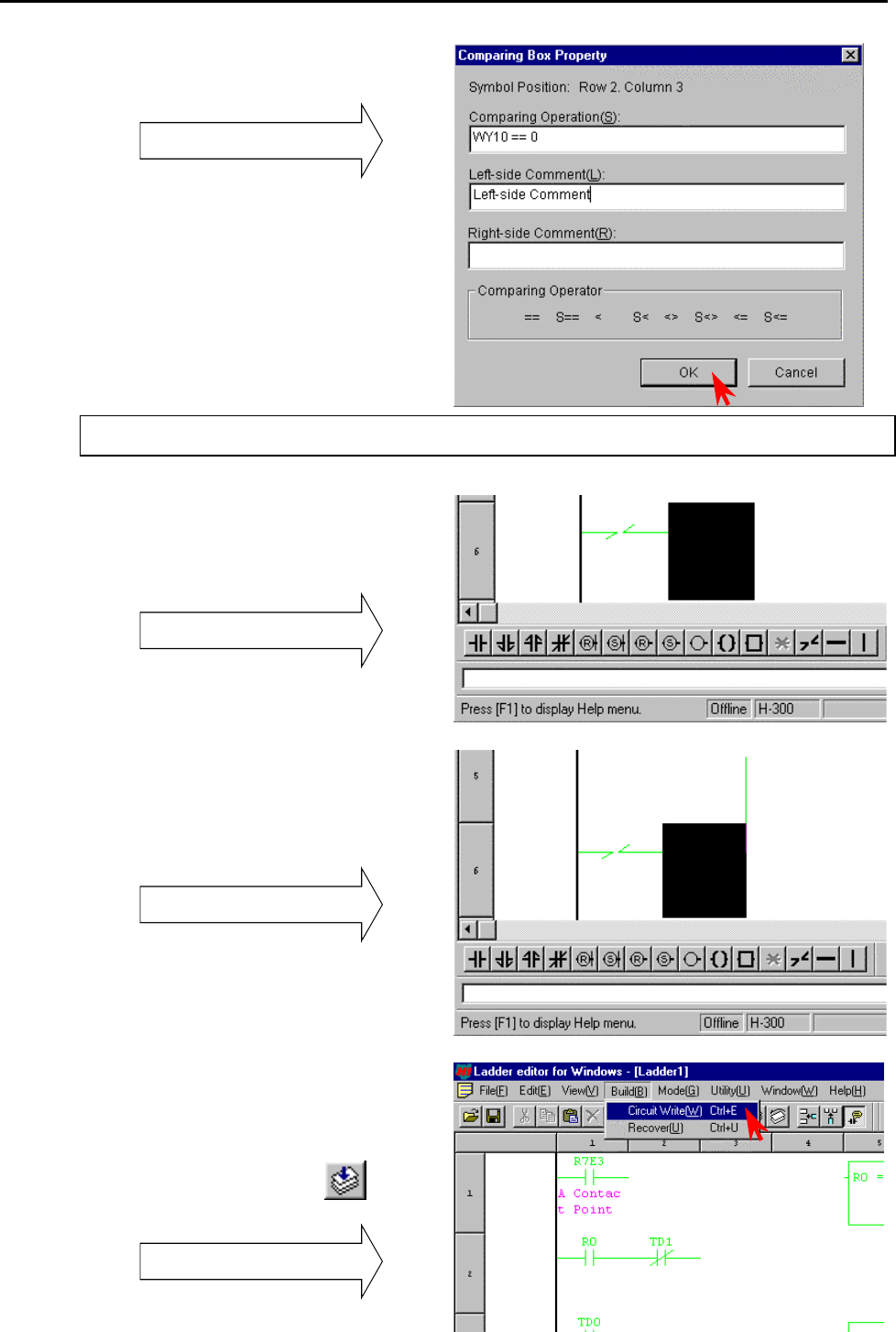
Chapter 14 Operation Examples
14-10
3] Input comparison expression and comment.
4] Click the [OK] button.
Comparison Box property
The comment input is valid only for I/O numbers.
In this example, entering a comment for the value
on the right side of the expression will not generate
a comment.
Always enter a space between an I/O number and comparison operator (in this case, between “WY10” and “= =“), as
well as between a comparison operator and comparison data (“= =“ and “0”).
[Example of entering a Knot]
1] Specify the input position.
2] Click the symbol for Knot.
The symbol is displayed and the cursor moves to
the right.
Display of symbols
[Example of entering a Vertical Line]
1] Specify the input position.
2] Click the symbol for Vertical Line.
The symbol is displayed on the right side of the
cursor.
The cursor does not move.
Display of symbol
In case of the Horizontal Line symbol, the cursor
does move to the right after displaying the symbol,
in the same way as in the Knot symbol.
2. Writing to the program memory
Perform a “circuit write” operation by either of the
following methods in order to write the circuit
to the program memory.
1] Click [Build] → [Circuit write] in the Menu
bar.
2] Click the [circuit write] icon in the
tool bar.
Circuit write operation
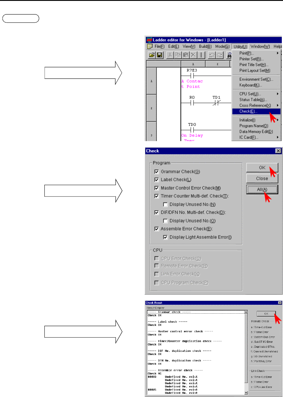
Chapter 14 Operation Examples
14-11
S T E P 4 Checking Program Errors
Check to see if the program in the memory is correct.
Click [Utility] → [Check] in the Menu bar.
The Check dialogue box is displayed.
Pull-down menu
•Click the [All items] or the individual check
column to specify the items to be checked.
•Click the [Execute] button.
The Check Result dialogue box is displayed.
Check dialogue box
The checking of the CPU can be specified at online
mode.
•Click the [OK] button.
The Check Result dialogue box closes.
Check Result dialogue box
(Note)
For example, if the I/O assignment of bit Y32 is
missing for unit 1, WY10 of the sample is treated
as undefined; the error is displayed as in the figure
to the right.
If there are any errors, correct the errors of the program before check the program again.
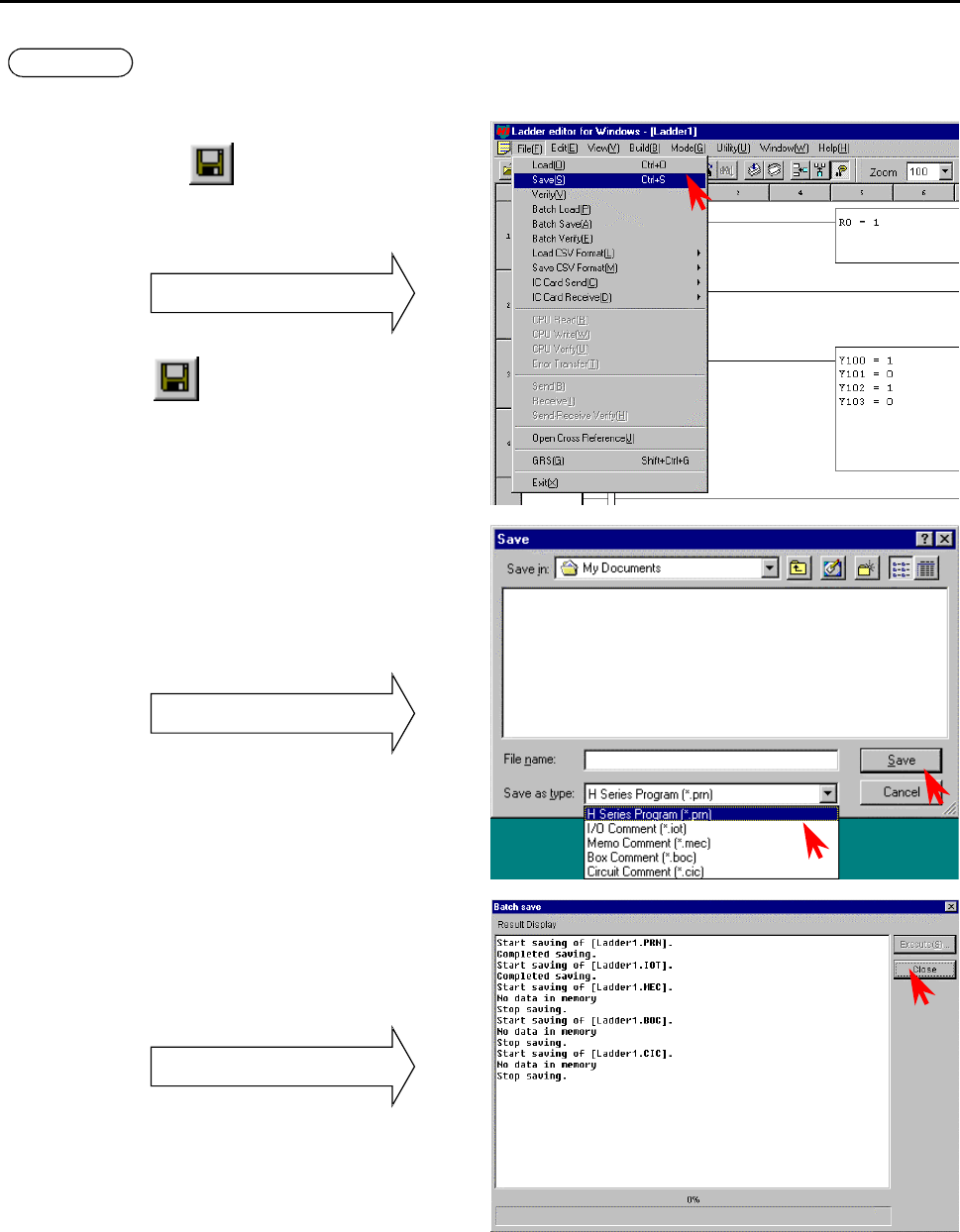
Chapter 14 Operation Examples
14-12
S T E P 5 Saving the Program
Save the program and comment that has been created to a floppy disk.
Click [File] → [Record] in the Menu bar, the
Record icon , or [File] → [Batch Record].
The dialogue for Record or Batch Record is
displayed.
Pull-down menu
Record : Specify the file type and save.
Batch Record: Saves a program and all the
comment files.
Record dialogue box:
Specify the directory to save in, file name, and
file type.
Batch Record dialogue box:
Specify the place to save and file name.
Click the [Save] button to save.
Record dialogue box
File name extensions are not necessary to input.
Record and Batch Record display the results of the
save operations for one file and five files
respectively.
The figure to the left shows an example of a result
display for the Batch Record.
Batch Record Result dialogue box
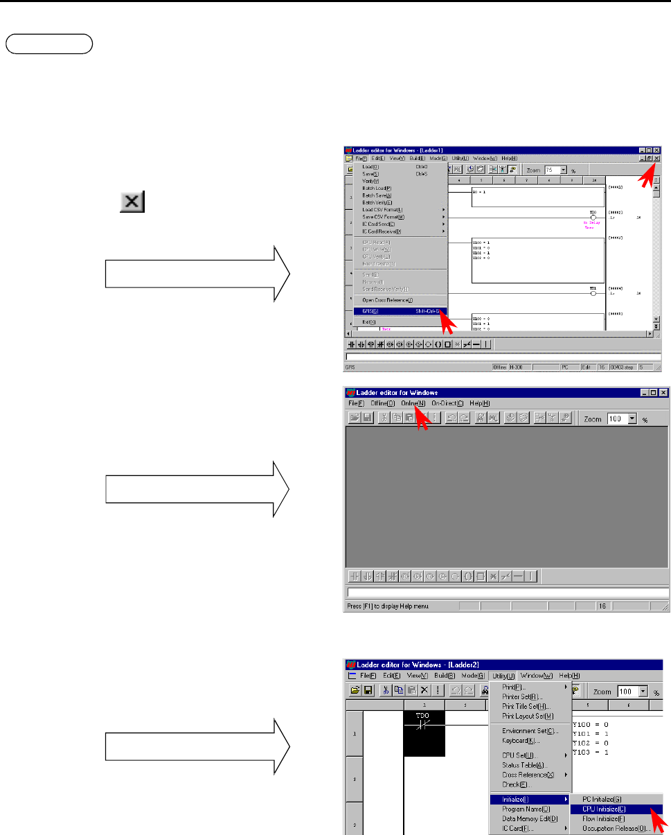
Chapter 14 Operation Examples
14-13
S T E P 6 Program Transfer to CPU
Write the program that has been input, to the CPU. However, verify the following:
•The CPU and the personal computer connection cable are properly connected.
•The CPU power is on.
•CPU mode switch is set to “STOP.”
1. Switching to online mode.
Move to the GRS screen from the offline mode.
This can be done in two ways.
1] Click [File] → [GRS] in the Menu bar.
2] Click (lower button) on the upper right of
the screen.
GRS screen
In the GRS screen, click the [Online] item in the
Menu bar.
The Read/Edit screen of the online mode is
displayed.
GRS screen
Note: Verify again that the DIP switches are set to
the transmission speed selected in the
Environment Setting in step 2. (For the 10-
point type, it is fixed to 4800 bps.)
2. Initializing the CPU
Click [Utility] → [Initialize] → [CPU initialize]
in the Menu bar.
Pull-down menu
Note: Please note that programs etc. in the personal
computer will be erased if [PC initialize] is
selected.
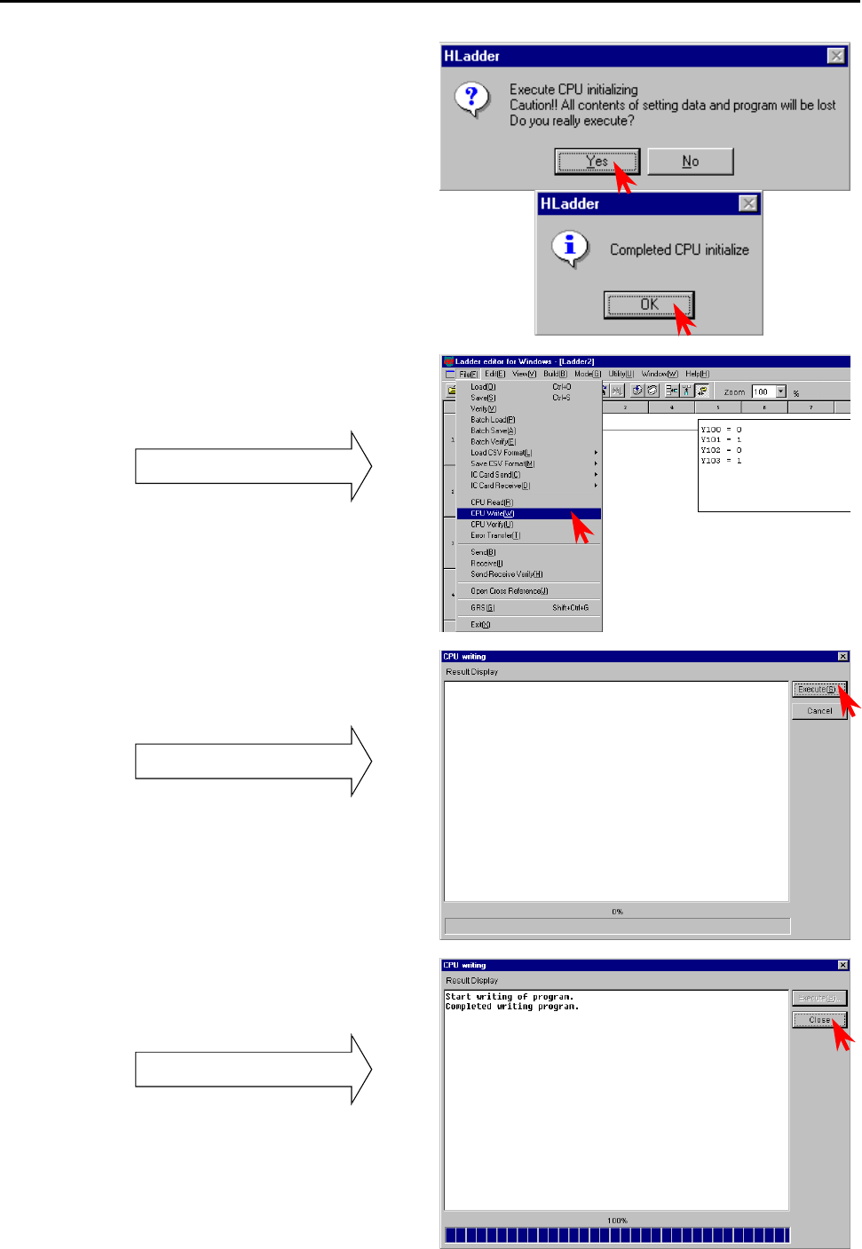
Chapter 14 Operation Examples
14-14
The Confirmation dialogue box is displayed; click
the [Yes] button and start the CPU initialization.
The Exit dialogue box is displayed; click the [OK]
button to close the dialogue.
3. Transferring to the CPU
Click [File] → [CPU write] in the Menu bar.
Pull-down menu
Program transfer
CPU Read: PC (personal computer) ← CPU
CPU Write: PC (personal computer) → CPU
The CPU Write dialogue box is displayed.
Click the [Execute] button.
CPU write dialogue box
When the writing is completed, the result is
displayed.
Click the [Close] button to close the dialogue box.
Display of write result
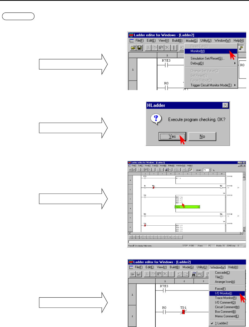
Chapter 14 Operation Examples
14-15
S T E P 7 Monitoring (Verifying the Operation)
Monitor the program execution status in the CPU.
[Circuit monitor]
Click [Mode] → [Monitor] in the Menu bar.
Pull-down menu
The Confirmation dialogue box for the program
match check between PC and the CPU is displayed.
Click the [Yes] button.
Match check
Set the CPU's RUN switch to “RUN” to begin the
CPU operation.
The on/off status of the contact, timer, and current
counter value are displayed.
Display of circuit monitor
To monitor and display the current value and
progress value, select comparison expression,
arithmetic box, and coil (timer, counter, etc.) with
the mouse arrow.
[I/O monitor]
The I/O monitor can be operated while in monitor
mode.
Click [Window] → [I/O Monitor] in the Menu
bar.
The I/O Monitor dialogue box is displayed.
Pull-down menu
The I/O Monitor dialogue box is displayed on the
Read/Edit screen at its maximum size.
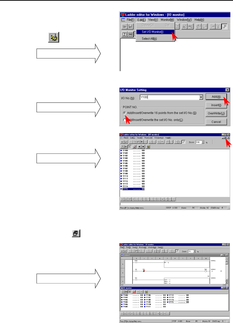
Chapter 14 Operation Examples
14-16
The I/O monitor can be specified in the following
two ways.
1] Click [Edit] → [I/O monitor setting] in the
Menu bar.
2] Click the icon in the Symbol bar.
I/O Monitor dialogue box
•Enter the starting I/O No.
•Click the number of points to be monitored.
•Click on either the [Add], [Insert], or
[Overwrite] buttons.
I/O Monitor Setting dialogue box
Monitor and display 16 points from Y100.
I/O monitor
The I/O monitor can display up to 64 I/O points (up
to 64 including words/double-words).
Click the I/O No. being I/O monitored and click
[Edit] → [Delete] to delete it from the monitor.
The display size of the I/O Monitor dialogue box
can be changed by clicking .
Both the circuit monitor in the Read/Edit screen
and the I/O Monitor can be displayed by making
their display sizes smaller to check the operation.
Display of circuit and I/O monitor

Chapter 15 Daily and Periodic Inspection
15-1
Chapter 15 Daily and Periodic Inspections
In order to use the functions of the MICRO-EH in the optimal conditions and maintain the system to operate normally, it
is essential to conduct daily and periodic inspections.
(1) Daily inspection
Verify the following items while the system is running.
Table 15.1 Items for daily inspection
Item LED
display Normal status Main cause of error
POW Lighting Power supply error, etc.
RUN Lighting
(in RUN
status)
When not lit:
Microcomputer malfunction, memory error, etc.
When flashing:
Syntax error, congestion error, etc.
Unit LED display
*1
OK Lighting When not lit:
Microcomputer malfunction, memory error, etc.
When flashing:
Battery error *2
*1: The MICRO-EH indicates the error contents using the combination of lit/flashing/not lit status of OK and
RUN lamps. For details, see the error code list in Chapter 12.
*2: If the power supply for the basic unit is left turned off without replacing the battery after the OK lamp was
flashing, the memory contents may be destroyed. Exercise caution when the system power is turned off for a
long period of time, since this error may not have been detected and the memory contents may have already
been destroyed.
(2) Periodic inspection
Turn off the power for the external I/O circuit and check the following items once every six months.
Table 15.2 Items for periodic inspection
Part Item Check criteria Remarks
Programming device to
CPU
Check operation of
programming device
Must be able to be connected online.
All switches and display lamps work
normally.
Power supply Check for voltage fluctuations 85 to 264 V AC Tester
I/O module Output relay life Electrical life 200,000 times
Mechanical life 20 million times
See the relay contact life
curve (Chapter 10).
LED Turns on/off correctly
External power voltage Within the specification for each I/O See the I/O specifications
(Chapter 6).
Battery
(Lithium battery)
Check voltage and life Is the OK lamp flashing?
Check to see if it has been less than
2 months since the last exchange.
Installation and
connecting areas
(1) All modules are securely
fixed
(2) All connectors fit snugly
(3) All screws are tightened
(4) Damage and deterioration
of each cable
There should be no problem. Tighten
Check insertion
Tighten
Visual check
Ambient environment (1) Temperature
(2) Humidity
(3) Other
0 to 55 °C
5 to 95 % RH (no condensation)
No dust, foreign matter, vibration
-
Spare parts Check number of parts, storage
condition
There should be no problem. -
Program Check program contents Compare the contents of the latest
program saved and CPU contents,
and make sure they match.
Check both master and
backup.
(3) Life of the power module
Numbers of electrolytic condensers are used in the power module. Electrolytic condensers have a lifetime and it is
believed that the life is reduced by half when the ambient temperature rises 10 °C.
When stocking spare parts, the standard for consideration is that the power module has a life of approximately five
years when used at the rated ambient temperature (30 °C). Also, to extend the life of the module, consider the air
circulation around the module and ambient temperature when installing it.
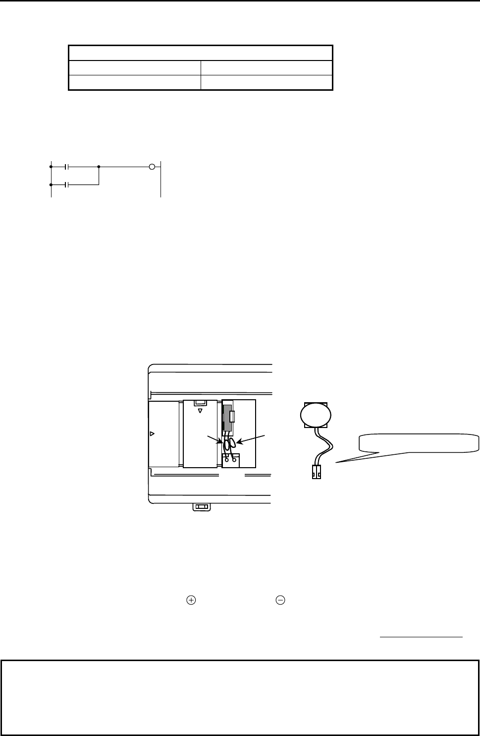
Chapter 15 Daily and Periodic Inspection
15-2
(4) Life of the battery
•The battery life time is shown below.
Battery life time (total power off time) [Hr] *
Guaranteed value (Min.) @55°C Actual value (Max.) @25°C
9,000 18,000
* Battery life time has been changed since Oct. 2002 production (MFG NO.02Jxx) due to hardware modification.
•The battery life can be determined by checking for the flashing of the OK lamp.
•The battery life time flag is in the bit special internal output “R7D9.”
An example of a circuit using “R7D9” is shown below.
R7D9
Y00100
Y00100
The battery error can be output to external output Y00100 by using
the ladder shown to the left.
* R7EE is a bit to enable battery error detection. Be sure to set R7EE
if battery is used.
Figure 15.1 Battery error detection circuit
•The self-diagnostic error code “71” indicates that the battery is not loaded or that it has reached its life.
•Exchange the battery every two years even if it is still functional.
•Use the battery within one year after purchase.
(5) How to replace the battery
Red
Blue
- +
Figure 15.2 Replacing battery
1] Prepare a new battery (EH-MBAT).
2] Replace the battery while the power supply to the basic base is turned on.
3] Remove the old lithium battery from the battery case.
4] Insert the new battery and connect the cable to the CPU module.
Insert it so that the red lead is , and the black lead is .
5] Fold the excess lead and store it in the lead storage space.
(If excess lead is not stored properly, the wire may get caught on the front cover and be severed.)
* When exchanging while the basic unit power turned off, perform steps 4], 5] and 6], in less than 30 minute.
Caution on handling the battery
Be careful when replacing the battery, since incorrect replacement may cause the battery to explode. Use EH-MBAT for new
batteries.
Batteries that have been replaced should be individually placed in a suitable plastic bag (to prevent shorting) and a disposal
company should be requested to dispose of them.
At this time, do not short the batteries, throw them in a fire, dismantle them, exert external force, expose them to water,
charge them or cut the lead wires since doing so leads to the risk that the batteries will ignite, explode or burn up.
Connector on batter
y
side

Appendix 1 H-series Instruction Support Comparison Chart
A-1
Appendix 1 H-Series Instruction Support
Comparison Chart
[Basic instructions and sequence instructions]
No. Instruction
format
Instruction name MICRO-
EH
EH-150 H-64
~
H-20
H-200 H-250 H-252 H-2000
H-700
H-300
H-2002
H-1002
H-702
H-302
H-4010
1 LD Start logical operation {{{{{{{{{
2 LDI Start logical NOT operation {{{{{{{{{
3 AND Logical AND {{{{{{{{{
4 ANI Logical AND not {{{{{{{{{
5 OR Logical OR {{{{{{{{{
6 ORI Logical OR not {{{{{{{{{
7 NOT Logical NOT {{{{{{{{{
8 AND DIF Detect rising edge {{{{{{{{{
9 OR DIF Detect rising edge {{{{{{{{{
10 AND DFN Detect falling edge {{{{{{{{{
11 OR DFN Detect falling edge {{{{{{{{{
12 OUT Output I/O {{{{{{{{{
13 SET Set I/O {{{{{{{{{
14 RES Reset I/O {{{{{{{{{
15 MCS Start master control {{{{{{{{{
16 MCR Cancel master control {{{{{{{{{
17 MPS Push operation result {{{{{{{{{
18 MRD Read operation result {{{{{{{{{
19 MPP Pull operation result {{{{{{{{{
20 ANB Connect logical block in serial {{{{{{{{{
21 ORB Connect logical block in parallel {{{{{{{{{
22 [ ] Start and end processing box {{{{{{{{{
23 ( ) Start and end relational box {{{{{{{{{
[Basic instructions and timers/counters]
No. Instruction
format
Instruction name MICRO-
EH
EH-150 H-64
~
H-20
H-200 H-250 H-252 H-2000
H-700
H-300
H-2002
H-1002
H-702
H-302
H-4010
1 OUT TD On-delay timer {{{{{{{{{
2 OUT SS Single shot {{{{{{{{{
3 OUT MS Mono stable timer ×{××
{{{{{
4 OUT TMR Integral timer ×{××
{{{{{
5 OUT WDT Watchdog timer ×{××
{{{{{
6 OUT CU Counter {{{{{{{{{
7 OUT RCU Ring counter ×{××
{{{{{
8 OUT CTU Up-down counter up {{{{{{{{{
9 OUT CTD Up-down counter down {{{{{{{{{
10 OUT CL Clear counter {{{{{{{{{

Appendix 1 H-series Instruction Support Comparison Chart
A-2
[Basic instructions and comparison boxes]
No. Instruction format Instruction name MICRO-
EH
EH-150 H-64
~
H-20
H-200 H-250 H-252 H-2000
H-700
H-300
H-2002
H-1002
H-702
H-302
H-4010
1 LD (s1 == s2) = comparison box {{{{{{{{{
2 AND (s1 == s2) = comparison box {{{{{{{{{
3 OR (s1 == s2) = comparison box {{{{{{{{{
4 LD (s1 S== s2) Signed = comparison box {{ ××
{{{{{
5 AND (s1 S== s2) Signed = comparison box {{ ××
{{{{{
6 OR (s1 S== s2) Signed = comparison box {{ ××
{{{{{
7 LD (s1 < > s2) < > comparison box {{{{{{{{{
8 AND (s1 < > s2) < > comparison box {{{{{{{{{
9 OR (s1 < > s2) < > comparison box {{{{{{{{{
10 LD (s1 S< > s2) Signed < > comparison box {{ ××
{{{{{
11 AND (s1 S< > s2) Signed < > comparison box {{ ××
{{{{{
12 OR (s1 S< > s2) Signed < > comparison box {{ ××
{{{{{
13 LD (s1 < s2) < comparison box {{{{{{{{{
14 AND (s1 < s2) < comparison box {{{{{{{{{
15 OR (s1 < s2) < comparison box {{{{{{{{{
16 LD (s1 S< s2) Signed < comparison box {{ ××
{{{{{
17 AND (s1 S< s2) Signed < comparison box {{ ××
{{{{{
18 OR (s1 S< s2) Signed < comparison box {{ ××
{{{{{
19 LD (s1 <= s2) <= comparison box {{{{{{{{{
20 AND (s1 <= s2) <= comparison box {{{{{{{{{
21 OR (s1 <= s2) <= comparison box {{{{{{{{{
22 LD (s1 S<= s2) Signed <= comparison box {{ ××
{{{{{
23 AND (s1 S<= s2) Signed <= comparison box {{ ××
{{{{{
24 OR (s1 S<= s2) Signed <= comparison box {{ ××
{{{{{

Appendix 1 H-series Instruction Support Comparison Chart
A-3
[Arithmetic instructions]
No. Instruction
format
Instruction name MICRO-
EH
EH-150 H-64
~
H-20
H-200 H-250 H-252 H-2000
H-700
H-300
H-2002
H-1002
H-702
H-302
H-4010
1 d = s Assignment statement {{{{{{{{{
2 d = s1 + s2 Binary addition {{{{{{{{{
3 d = s1 B+ s2 BCD addition {{{{{{{{{
4 d = s1 – s2 Binary subtraction {{{{{{{{{
5 d = s1 B– s2 BCD subtraction {{{{{{{{{
6 d = s1 × s2 Binary multiplication {{{{{{{{{
7 d = s1 B× s2 BCD multiplication {{{{{{{{{
8 d = s1 S× s2 Signed binary multiplication {{ ××
{{{{{
9 d = s1 / s2 Binary division {{{{{{{{{
10 d = s1 B/ s2 BCD division {{{{{{{{{
11 d = s1 S/ s2 Signed binary division {{ ××
{{{{{
12 d = s1 OR s2 Logical OR {{{{{{{{{
13 d = s1 AND s2 Logical AND {{{{{{{{{
14 d = s1 XOR s2 Exclusive OR {{{{{{{{{
15 d = s1 == s2 = comparison expression {{{{{{{{{
16 d = s1 S== s2 Signed = comparison expression {{ ××
{{{{{
17 d = s1 < > s2 ≠ comparison expression {{{{{{{{{
18 d = s1 S< > s2 Signed ≠ comparison expression {{ ××
{{{{{
19 d = s1 < s2 < comparison expression {{{{{{{{{
20 d = s1 S< s2 Signed < comparison expression {{ ××
{{{{{
21 d = s1 <= s2 ≤ comparison expression {{{{{{{{{
22 d = s1 S<= s2 Signed ≤ comparison expression {{ ××
{{{{{
[Application instructions] (1/2)
No. Instruction
format
Instruction name MICRO-
EH
EH-150 H-64
~
H-20
H-200 H-250 H-252 H-2000
H-700
H-300
H-2002
H-1002
H-702
H-302
H-4010
1 BSET (d, n) Bit set {{{{{{{{{
2 BRES (d, n) Bit reset {{{{{{{{{
3 BTS (d, n) Bit test {{{{{{{{{
4 SHR (d, n) Shift right {{{{{{{{{
5 SHL (d, n) Shift left {{{{{{{{{
6 ROR (d, n) Rotate right {{{{{{{{{
7 ROL (d, n) Rotate left {{{{{{{{{
8 LSR (d, n) Logical shift right {{{{{{{{{
9 LSL (d, n) Logical shift left {{{{{{{{{
10 BSR (d, n) BCD shift right {{{{{{{{{
11 BSL (d, n) BCD shift left {{{{{{{{{
12 WSHR (d, n) Batch shift right ×{××
{{{{{
13 WSHL (d, n) Batch shift left ×{××
{{{{{
14 WBSR (d, n) Batch BCD shift right ×{××
{{{{{
15 WBSL (d, n) Batch BCD shift left ×{××
{{{{{
16 MOV (d, s, n) Block transfer {{ ××
{{{{{
17 COPY (d, s, n) Copy {{ ××
{{{{{

Appendix 1 H-series Instruction Support Comparison Chart
A-4
[Application instructions] (2/2)
No. Instruction
format
Instruction name MICRO-
EH
EH-150 H-64
~
H-20
H-200 H-250 H-252 H-2000
H-700
H-300
H-2002
H-1002
H-702
H-302
H-4010
18 XCG (d, d2, n) Block exchange {{ ××
{{{{{
19 NOT (d) Reverse {{{{{{{{{
20 NEG (d) Two's complement {{{{{{{{{
21 ABS (d, s) Absolute value {{{{{{{{{
22 SGET (d, s) Sign addition ×{××
{{{{{
23 EXT (d, s) Sign expansion ×{××
{{{{{
24 BCD (d, s) Binary → BCD conversion {{{{{{{{{
25 BIN (d, s) BCD → Binary conversion {{{{{{{{{
26 DECO (d, s, n) Decode {{{{{{{{{
27 ENCO (d, s, n) Encode {{{{{{{{{
28 SEG (d, s) 7 segment decode ×{××
{{{{{
29 SQR (d, s) Square root ×{××
{{{{{
30 BCU (d, s) Bit count {{{{{{{{{
31 SWAP (d) Swap {{{{{{{{{
32 FIFIT (P, n) Initialize FIFO ×{××
{{{{{
33 FIFWR (P, s) Write FIFO ×{××
{{{{{
34 FIFRD (P, d) Read FIFO ×{××
{{{{{
35 UNIT (d, s, n) Unit {{{{{{{{{
36 DIST (d, s, n) Distribute {{{{{{{{{
37 ADRIO (d, s) Convert I/O address ×{×××
{{{{
[Control instructions]
No. Instruction
format
Instruction name MICRO-
EH
EH-150 H-64
~
H-20
H-200 H-250 H-252 H-2000
H-700
H-300
H-2002
H-1002
H-702
H-302
H-4010
1 END End normal scan {{{{{{{{{
2 CEND (s) End scan condition {{{{{{{{{
3 JMP n Unconditional jump {{{{{{{{{
4 CJMP n (s) Conditional jump {{{{{{{{{
5 RSRV n Reserve ××××××
{{{
6 FREE Free reserve ××××××
{{{
7LBL n Label {{{{{{{{{
8FOR n (s) For {{ ××
{{{{{
9NEXT n Next {{ ××
{{{{{
10 CAL n Call subroutine {{{{{{{{{
11 SB n Start subroutine program {{{{{{{{{
12 RTS Return subroutine {{{{{{{{{
13 START n Start basic task ××××××
{{{
14 INT n Start interrupt scan program {{{{{{{{{
15 RTI Return interrupt {{{{{{{{{

Appendix 1 H-series Instruction Support Comparison Chart
A-5
[High-function module transfer instructions]
No. Instruction
format
Instruction name MICRO-
EH
EH-150 H-64
~
H-20
H-200 H-250 H-252 H-2000
H-700
H-300
H-2002
H-1002
H-702
H-302
H-4010
1 TRNS 0 (d, s, t) General-purpose port transmission
instruction
{*{×××××
{{
2 RECV 0 (d, s, t) General-purpose port reception
instruction
{*{×××××
{{
3 TRNS 1 (d, s, t) Data transmission/reception
instruction for SIO, CLOCK
×××××
{×{{
4 QTRNS1 (d, s, t) High-speed data
transmission/reception instruction for
SIO, CLOCK
×××××××
{{
5 TRNS 2 (d, s, t) Data transmission/reception
instruction for ASCII
×××××××
{{
6 QTRNS2 (d, s, t) High-speed data
transmission/reception instruction for
ASCII
×××××××
{{
7 TRNS 3 (d, s, t) Data transmission instruction for
POSIT-H
×××××××
{{
8 QTRNS3 (d, s, t) High-speed data transmission
instruction for POSIT-H
×××××××
{{
9 RECV 3 (d, s, t) Data reception instruction for POSIT-
H
×××××××
{{
10 TRNS 4 (d, s, t) Data transmission/reception
instruction for POSIT-2H,
POSITA2H
×××××
{×{{
11 QTRNS 4 (d, s, t) High-speed data
transmission/reception instruction for
POSIT-2H, POSITA2H
×××××××
{{
12 TRNS 5 (d, s, t) Data transmission/reception
instruction for XCU-001H
×××××××
{{
13 TRNS 6 (d, s, t) Data transmission/reception
instruction for XCU-232H
×××××××
{{
* Supported by software version 1.30 (WRF051=H0130) or newer.
[FUN instructions] (1/5)
No. Instruction
format
Instruction name MICRO-
EH
EH-150 H-64
~
H-20
H-200 H-250 H-252 H-2000
H-700
H-300
H-2002
H-1002
H-702
H-302
H-4010
1FUN 0 (s)
(PIDIT (s))
PID operation initialization ×{×××
{×{{
2FUN 1 (s)
(PIDOP (s))
PID operation execution control ×{×××
{×{{
3FUN 2 (s)
(PIDCL (s))
PID operation execution ×{×××
{×{{
4FUN 4 (s)
(IFR (s))
Process stepping ×{××××××
{
5 FUN 5 (s) General purpose port switching {××××××××
6 FUN 10 (s)
(SIN (s))
SIN function calculation ×{×××
{×{{
7 FUN 11 (s)
(COS (s))
COS function calculation ×{×××
{×{{
8 FUN 12 (s)
(TAN (s))
TAN function calculation ×{×××
{×{{
9 FUN 13 (s)
(ASIN (s))
ARC SIN function calculation ×{×××
{×{{
10 FUN 14 (s)
(ACOS (s))
ARC COS function calculation ×{×××
{×{{
11 FUN 15 (s)
(ATAN (s))
ARC TAN function calculation ×{×××
{×{{
12 FUN 20 (s)
(DSRCH (s))
Data search ×××××
{×{{
13 FUN 21 (s)
(TSRCH (s))
Table search ×××××
{×{{
14 FUN 30 (s)
(BINDA (s))
Binary → decimal ASCII conversion
(16 bits)
×××××
{×{{
15 FUN 31 (s)
(DBINDA (s))
Binary → decimal ASCII conversion
(32 bits)
×××××
{×{{

Appendix 1 H-series Instruction Support Comparison Chart
A-6
[FUN instructions] (2/5)
No. Instruction
format
Instruction name MICRO-
EH
EH-150 H-64
~
H-20
H-200 H-250 H-252 H-2000
H-700
H-300
H-2002
H-1002
H-702
H-302
H-4010
16 FUN 32 (s)
(BINHA (s))
Binary → hexadecimal ASCII
conversion (16 bits)
×××××
{×{{
17 FUN 33 (s)
(DBINHA (s))
Binary → hexadecimal ASCII
conversion (32 bits)
×××××
{×{{
18 FUN 34 (s)
(BCDDA (s))
BCD → decimal ASCII conversion
(16 bits)
×××××
{×{{
19 FUN 35 (s)
(DBCDDA (s))
BCD → decimal ASCII conversion
(32 bits)
×××××
{×{{
20 FUN 36 (s)
(DABIN (s))
Unsigned 5 digit
Decimal ASCII → binary conversion
×××××
{×{{
21 FUN 37 (s)
(DDABIN (s))
Signed 10 digit
Decimal ASCII → binary conversion
×××××
{×{{
22 FUN 38 (s)
(HABIN (s))
4-digit hexadecimal ASCII → binary
conversion
×××××
{×{{
23 FUN 39 (s)
(DHABIN (s))
8-digit hexadecimal ASCII → binary
conversion
×××××
{×{{
24 FUN 40 (s)
(DABCD (s))
4-digit decimal ASCII → BCD
conversion
×××××
{×{{
25 FUN 41 (s)
(DDABCD (s))
8-digit decimal ASCII → BCD
conversion
×××××
{×{{
26 FUN 42 (s)
(ASC (s))
Hexadecimal binary → ASCII
conversion (digit designation)
×××××
{×{{
27 FUN 43 (s)
(HEX (s))
Hexadecimal ASCII → binary
conversion (digit designation)
×××××
{×{{
28 FUN 44 (s)
(ASDD (s))
Unit character strings ×××××
{×{{
29 FUN 45 (s)
(SCMP (s))
Compare character strings ×××××
{×{{
30 FUN 46 (s)
(WTOB (s))
Word → byte conversion ×××××
{×{{
31 FUN 47 (s)
(WTOW (s))
Byte → word conversion ×××××
{×{{
32 FUN 48 (s)
(BSHR (s))
Shift byte unit to right ×××××
{×{{
33 FUN 49 (s)
(BSHL (s))
Shift byte unit to left ×××××
{×{{
34 FUN 50 (s)
(TRSET (s))
Set sampling trace ×××××
{×{{
35 FUN 51 (s)
(TRACE (s))
Execute sampling trace ×××××
{×{{
36 FUN 52 (s)
(TRRES (s))
Reset sampling trace ×××××
{×{{
37 FUN 60 (s)
(BSQR (s))
Binary square root ×××××
{×{{
38 FUN 61 (s)
(PGEN (s))
Dynamic scan pulse ×××××
{×{{
39 FUN 70 (s) Set high-speed counter mode ××
{××××××
40 FUN 71 (s) Read high-speed counter progress
value
××
{××××××
41 FUN 72 (s) Write high-speed counter progress
value
××
{××××××
42 FUN 73 (s) Read high-speed counter set value ××
{××××××
43 FUN 74 (s) Write high-speed counter set value ××
{××××××
44 FUN 80 (s)
(ALREF (s))
Refresh I/O (all points) {{ ×××
{××
{

Appendix 1 H-series Instruction Support Comparison Chart
A-7
[FUN instructions] (3/5)
No. Instruction
format
Instruction name MICRO-
EH
EH-150 H-64
~
H-20
H-200 H-250 H-252 H-2000
H-700
H-300
H-2002
H-1002
H-702
H-302
H-4010
45 FUN 81 (s)
(IORREF (s))
Refresh I/O
(input/output designation)
{{ ×××
{××
{
46 FUN 82 (s)
(SLREL (s))
Refresh I/O refresh (any slot) {{ ×××
{××
{
47 FUN 90
(ETDIT)
Expansion timer initial setting ××××××××
{
48 FUN 91
(ETD)
Expansion timer execution ××××××××
{
49 FUN 92
(ECUIT)
Expansion counter/up-down counter
initial setting
×××××××××
50 FUN 93
(ECU)
Expansion counter execution ×××××××××
51 FUN 94
(ECTU)
Expansion up-down counter up
execution
×××××××××
52 FUN 95
(ECTD)
Expansion up-down counter down
execution
×××××××××
53 FUN 96
(ECL)
Clear expansion counter ×××××××××
54 FUN 97
(WNRED)
Read expansion link area ××××××××
{
55 FUN 98
(WNWRT)
Write expansion link area ××××××××
{
56 FUN 100
(INT)
Floating decimal point operation
(real number → integer (word )
conversion)
×{××××××
{
57 FUN 101
(INTD)
Floating decimal point operation
(real number → integer (double word)
conversion)
×{××××××
{
58 FUN 102
(FLOAT)
Floating decimal point operation
(integer (word) → real number
conversion)
×{××××××
{
59 FUN 103
(FLOATD)
Floating decimal point operation
(integer (double word) → real number
conversion)
×{××××××
{
60 FUN 104
(FADD)
Floating decimal point operation
(addition)
×{××××××
{
61 FUN 105
(FSUB)
Floating decimal point operation
(subtraction)
×{××××××
{
62 FUN 106
(FMUL)
Floating decimal point operation
(multiplication)
×{××××××
{
63 FUN 107
(FDIV)
Floating decimal point operation
(division)
×{××××××
{
64 FUN 108
(FRAD)
Floating decimal point operation
(angle → radian conversion)
×{××××××
{
65 FUN 109
(FDEG)
Floating decimal point operation
(radian → angle conversion)
×{××××××
{
66 FUN 110
(FSIN)
Floating decimal point operation
(SIN)
×{××××××
{
67 FUN 111
(FCOS)
Floating decimal point operation
(COS)
×{××××××
{
68 FUN 112
(FTAN)
Floating decimal point operation
(TAN)
×{××××××
{
69 FUN 113
(FASIN)
Floating decimal point operation
(ARC SIN)
×{××××××
{
70 FUN 114
(FACOS)
Floating decimal point operation
(ARC COS)
×{××××××
{

Appendix 1 H-series Instruction Support Comparison Chart
A-8
[FUN instructions] (4/5)
No. Instruction
format
Instruction name MICRO-
EH
EH-150 H-64
~
H-20
H-200 H-250 H-252 H-2000
H-700
H-300
H-2002
H-1002
H-702
H-302
H-4010
71 FUN 115
(FATAN)
Floating decimal point operation
(ARC TAN)
×{××××××
{
72 FUN 116
(FSQR)
Floating decimal point operation
(square root)
×{××××××
{
73 FUN 117
(FEXP)
Floating decimal point operation
(exponent)
×{××××××
{
74 FUN 118
(FLOG)
Floating decimal point operation
(natural logarithm)
×{××××××
{
75 FUN 120
(INDXD)
Index setting (argument d) ××××××××
{
76 FUN 121
(INDXS)
Index setting (argument s) ××××××××
{
77 FUN 122
(INDXC)
Cancel index ××××××××
{
78 FUN 123
(INC)
Increment (INC) ××××××××
{
79 FUN 124
(INCD)
Double word increment (DINC) ××××××××
{
80 FUN 125
(DEC)
Decrement (DEC) ××××××××
{
81 FUN 126
(DECD)
Double word decrement (DECD) ××××××××
{
82 FUN 127
(BITTOW)
Expand bit data to word data ××××××××
{
83 FUN 128
(WTOBIT)
Expand word data to bit data ××××××××
{
84 FUN 130
(FBINI)
Set file memory block ××××××××
{
85 FUN 131
(FBMOV)
Transfer file memory block ××××××××
{
86 FUN 132
(FBCHG)
Exchange file memory block ××××××××
{
87 FUN 133
(FWRED)
Read file memory word unit ××××××××
{
88 FUN 134
(FWWRT)
Write file memory word unit ××××××××
{
89 FUN 135
(FRED)
Read file memory byte unit ××××××××
{
90 FUN 136
(FWRT)
Write file memory byte unit ××××××××
{
91 FUN 140 (s) High-speed counter operation control {××××××××
92 FUN 141 (s) High-speed counter coincident output
control
{××××××××
93 FUN 142 (s) High-speed counter up/down control {××××××××
94 FUN 143 (s) Rewrite current high-speed counter
value
{××××××××
95 FUN 144 (s) Read current high-speed counter
value
{××××××××
96 FUN 145 (s) Clear current high-speed counter
value
{××××××××

Appendix 1 H-series Instruction Support Comparison Chart
A-9
[FUN instructions] (5/5)
No. Instruction
format
Instruction name MICRO-
EH
EH-150 H-64
~
H-20
H-200 H-250 H-252 H-2000
H-700
H-300
H-2002
H-1002
H-702
H-302
H-4010
97 FUN 146 (s) Preset high-speed counter {××××××××
98 FUN 147 (s) PWM operation control {××××××××
99 FUN 148 (s) Change PWM frequency on-duty {××××××××
100 FUN 149 (s) Pulse output control {××××××××
101 FUN 150 (s) Change number of pulse frequency
output setting
{××××××××
102 FUN 151 (s) Pulse output with
acceleration/deceleration
{××××××××
103 FUN 210 (s)
(LOGIT (s))
Initial setting for data logging ×{×××××××
104 FUN 211 (s)
(LOGWRT (s))
Write log data ×{×××××××
105 FUN 212 (s)
(LOGCLR (s))
Clear log data ×{×××××××
106 FUN 213 (s)
(LOGRED (s))
Read log data ×{×××××××
107 FUN 254 (s)
(BOXC (s))
BOX comment {{{{{{{{{
108 FUN 255 (s)
(MEMC (s))
Memo comment {{{{{{{{{
Supported command for EH-150 depends on CPU types. Please read EH-150 application manual for further information.

Appendix 2 Standards
A-11
Appendix 2 Standards
MICRO-EH products are global products designed and manufactured for use throughout the world. They should be installed and
used in conformance with product-specific guidelines as well as the following agency approvals and standards.
Item Standards
Industrial Control
Equipment[Safety]
UL 508
CSA C22.2 no 142-M1987
Certification by Underwriters Laboratories for
selected modules
Hazardous Locations[Safety]
Class I, Div II, A,B,C,D
UL 1604
CSA C22.2 No142-M1987
Certification by Underwriters Laboratories for
selected modules
European EMC Directive IEC 61131-2 (2003) Emission, Immunity
European Low Voltage Directive IEC 61131-2 (1994)
Australia C-tick mark AS/AZN CISPR11 (2002)
Warning:
Explosion hazard – substitution of componets may impair suitability for class I, division 2"
Do not replace modules unless power has been switched off or the area is known to be non-hazardous.
Do not disconnect equipment unless power has been switched off or the area is known to be non-hazardous.
