Honeycomb Technologies HBT24B13AN Bluetooth Module User Manual manual
Shenzhen Honeycomb Technologies Company Limited Bluetooth Module manual
User Manual

HBT24B13AN
©2013 Honeycomb Technologies Advance Information Page 1
HBT24B13AN
Data Sheet

HBT24B13AN
©2013 Honeycomb Technologies Advance Information Page 2
Note the label artwork for Products
Warning: Changes or modifications to this unit not expressly approved by the party
responsible for compliance could void the user’s authority to operate the equipment.
NOTE: This equipment has been tested and found to comply with the limits for a Class B
digital device, pursuant to Part 15 of the FCC Rules. These limits are designed to provide
reasonable protection against harmful interference in a residential installation. This
equipment generates, uses and can radiate radio frequency energy and, if not installed and
used in accordance with the instructions, may cause harmful interference to radio
communications.
However, there is no guarantee that interference will not occur in a particular installation. If
this equipment does cause harmful interference to radio or television reception, which can be
determined by turning the equipment off and on, the user is encouraged to try to correct the
interference by one or more of the following measures:
Reorient or relocate the receiving antenna.
Increase the separation between the equipment and receiver.
Connect the equipment into an outlet on a circuit different from that to which the
receiver is connected.
Consult the dealer or an experienced radio/TV technician for help.

HBT24B13AN
©2013 Honeycomb Technologies Advance Information Page 3
Note: This BT Module is designed to be used internally only in Controls products
which with RF shielding. It is not intended to be sold as an end item by itself to
external customers.
FCC Caution: Any changes or modifications not expressly approved by the party
responsible for compliance could void the user’s authority to operate this
equipment.
This module and its antenna(s) must not be co-located with any other transmitters
except in accordance with FCC multi-transmitter product procedures.
The module is intended only for OEM integrator. And it should not be marketed
and sold in a way that has to be end-user accessible / replaceable. The host
product is required to comply with all applicable FCC equipment authorizations
regulations, requirements and equipment functions not associated with the
transmitter module portion. The host manufacturer is responsible for ensuring
compliance with the module(s) installed and fully operational.
Label of the end product:
The final end product must be labeled in a visible area with the following “Contains
Transmitter Module FCC ID: 2AAUWHBT24B13AN” or “Contains FCC ID:
2AAUWHBT24B13AN”. If the size of the end product is larger than 8*10cm, then
the following FCC Part 15.19 statement has to also be available on the label: This
device complies with Part 15 of the FCC Rules. Operation is subject to the following
two conditions: (1) this device may not cause harmful interference, and (2) this
device must accept any interference received, including interference that may
cause undesired operation.
User manual of the end product:
In the user manual of the end product, the end user has to be informed that:
Warning: Changes or modifications to this unit not expressly approved by the party
responsible for compliance could void the user’s authority to operate the equipment.
NOTE: This equipment has been tested and found to comply with the limits for a Class B
digital device, pursuant to Part 15 of the FCC Rules. These limits are designed to provide
reasonable protection against harmful interference in a residential installation. This
equipment generates, uses and can radiate radio frequency energy and, if not installed and
used in accordance with the instructions, may cause harmful interference to radio
communications.
However, there is no guarantee that interference will not occur in a particular installation. If
this equipment does cause harmful interference to radio or television reception, which can be
determined by turning the equipment off and on, the user is encouraged to try to correct the
interference by one or more of the following measures:

HBT24B13AN
©2013 Honeycomb Technologies Advance Information Page 4
Reorient or relocate the receiving antenna.
Increase the separation between the equipment and receiver.
Connect the equipment into an outlet on a circuit different from that to which the
receiver is connected.
Consult the dealer or an experienced radio/TV technician for help.
If the size of the end product is smaller than 8*10cm, then additional FCC Part
15.19 statement is required to be available in the user manual: This device
complies with Part 15 of the FCC Rules. Operation is subject to the following two
conditions: (1) this device may not cause harmful interference, and (2) this device
must accept any interference received, including interference that may cause
undesired operation.

HBT24B13AN
©2013 Honeycomb Technologies Advance Information Page 5
BlueTooth 2.1+EDR Module
Features:
On-chip TX/RX switch
Small Size: 27mm*13mm Surface Mountable.
Polar modulation transmitter architecture with very low power
consumption high TX performance.
Near-Zero IF receiver architecture with 91dBm sensitivity.
Support for class 1, 2 and 3 transmitting power requirement.
Fully integrated synthesizer without external loop filter component.
Operational:
Operating Voltage: 3.2V to 4.3V(typical 3.3V )
Temperature Range: -20°C to +70°C
Simple, Four-Wire SPI Interface
BASEBAND
Fully compliant with Bluetooth 2.1 + EDR specification.
Support Bluetooth Piconet and Scatternet.
Support up to 3Mbps high speed UART interface.
Support Sniff mode, hold mode and park mode.
Support A-law, μ-law and CVSD digitize audio CODEC in PCM
interface
HBT24B13AN
©2013 Honeycomb Technologies Advance Information Page 6
Provide 4 wires SPI interface.
DEVICE
Enhanced support for WLAN/BT Co-existence.
Standby and sleep modes to minimize power consumption.
Support share handset system reference clock.
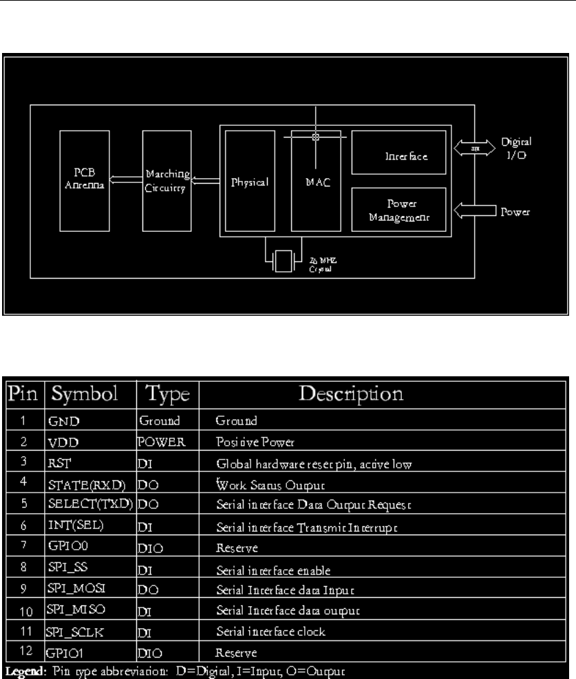
FIGURE 1: PIN DIAGRAM
Device Overview
The BK3211 chip is a highly integrated single-chip Bluetooth device. It
integrates the high-performance transceiver and rich features baseband
processor, which is compliant with Bluetooth 2.1 + EDR specification
HBT24B13AN
©2013 Honeycomb Technologies Advance Information Page 7
FIGURE 2: BLOCK DIAGRAM
TABLE 1-1: PIN DESCRIPTION
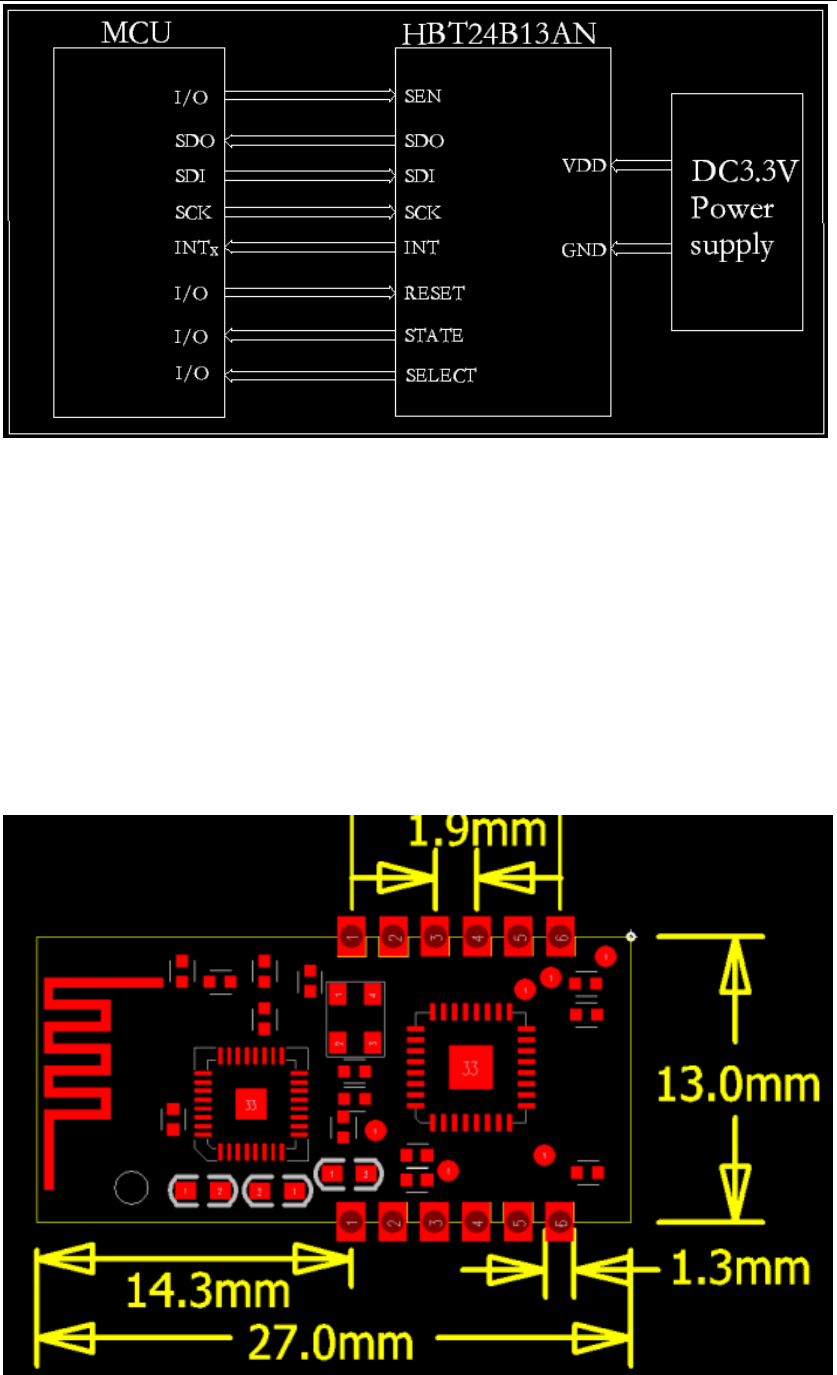
FIGURE 3: MICROCONTROLLER TO HBT24B13AN INTERFACE
HBT24B13AN
©2013 Honeycomb Technologies Advance Information Page 8
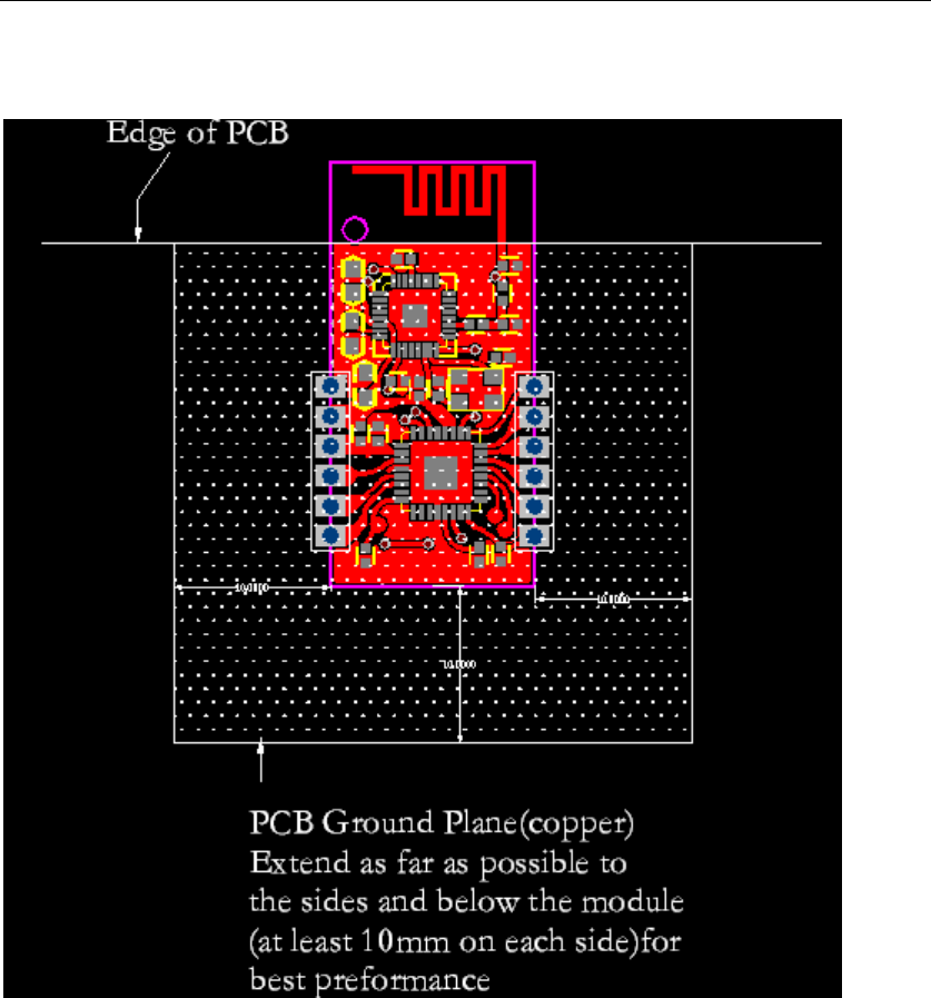
Mounting Details
The HBT24B13AN is a surface mountable module. Module dimensions are shown in
Figure 4. The module Printed Circuit Board (PCB) is 0.032" thick with castellated
mounting holes on the edge. Figure5 is a recommended host PCB footprint for the
HBT24B13AN. The HBT24B13AN has an integrated PCB antenna. For the best
performance, follow the mounting details shown in Figure 5. It is recommended that
the module be mounted on the edge of the host PCB and an area around the
antenna, approximately 1.2", be kept clear of metal objects. A host PCB ground plane
around the HBT24B13AN acts as a counterpoise to the PCB antenna. It is
recommended to extend the ground plane at least 0.4" around the module.
FIGURE 4: MODULE DETAILS
HBT24B13AN
©2013 Honeycomb Technologies Advance Information Page 9
FIGURE 5 RECOMMENDED PCB FOOTPRINT
CIRCUIT DESCRIPTION
The HBT24B13AN module is a compliant with Bluetooth 2.1 + EDR surface mount
module with integrated crystal, internal voltage regulator, matching circuitry and PCB
antenna. The HBT24B13AN module interfaces to many popular micro-controllers via
a 4-wire serial SPI interface, interrupt, wake, Reset, power and ground.
HBT24B13AN
©2013 Honeycomb Technologies Advance Information Page 10
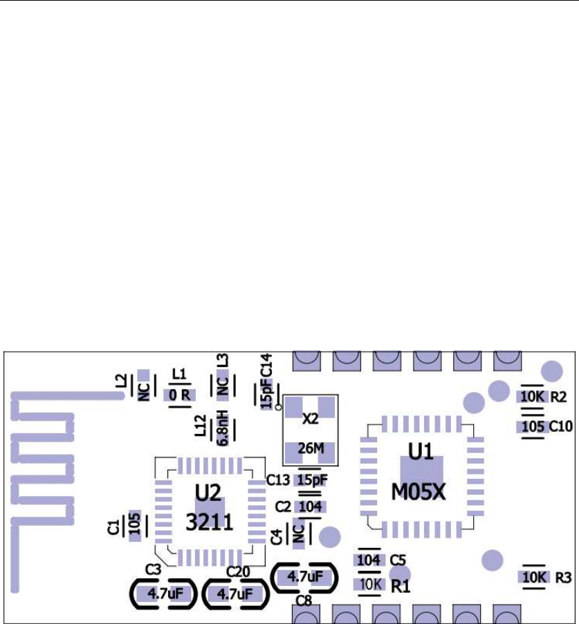
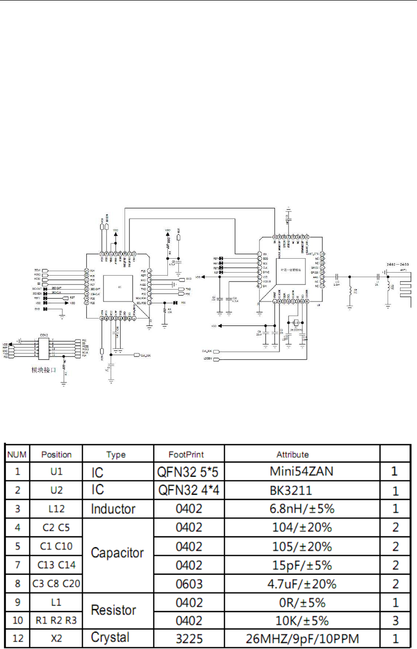
SCHEMATIC
A schematic diagram of the module is shown in Figure 6 and the Bill of Materials
(BOM) is shown in Table 2. The HBT24B13AN module is based on the BK3211 chip is a
highly integrated single-chip Bluetooth device. ceiver IC. The serial I/O (SCK, SDI, SDO
and CS), RESET, STATE, SELECT and INT pins are brought out to the module pins. The
SDO signal is tri-state buffered by IC2 to solve a silicon errata where the SDO signal
does not release to a high-impedance state after the CS pin returns to its inactive
state. Crystal Y1 is a 26 MHz crystal with a frequency tolerance of ±20 ppm @ 25°C to
±40 ppm.
FIGURE 6 HBT24B13AN SCHEMATIC
TABLE 2
HBT24B13AN BILL OF MATERIALS
HBT24B13AN
©2013 Honeycomb Technologies Advance Information Page 11
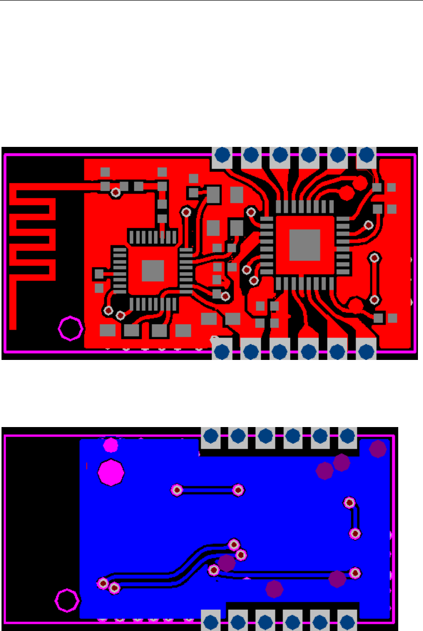
Printed Circuit Board
The HBT24B13AN module printed circuit board is con-structed with FR4 material,
two layers and 0.8mm thick. The layers are shown in Figure 7 through Figure 8. The
stack up of the PCB is shown in Figure9
FIGURE 7 TOP COPPER
FIGURE 8 BOTTOM COPPER
HBT24B13AN
©2013 Honeycomb Technologies Advance Information Page 12
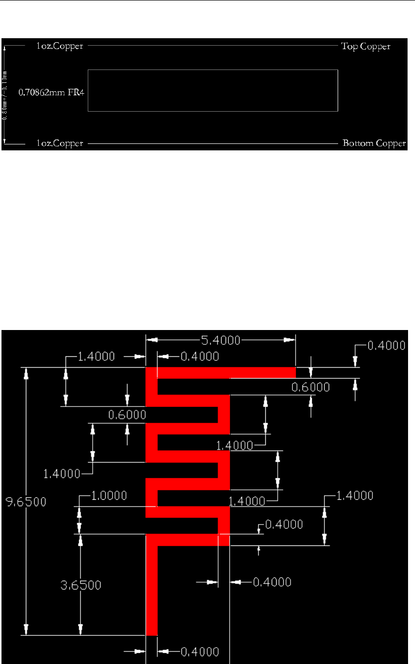
FIGURE 9 PCB LAYER STACK UP
PCB Antenna
The PCB antenna is fabricated on the top copper trace. Figure 10 shows the trace
dimensions. The layers below the antenna have no copper traces. The ground and
power planes under the components serve as a counterpoise to the PCB antenna.
Additional ground plane on the host PCB will substantially enhance the performance
of the module.
FIGURE 10 PCB LAYER STACK UP