Hosiden CFU0321 802.15.4 ZigBee RF Module User Manual CFU0321Product Datasheet
Hosiden Corporation 802.15.4 ZigBee RF Module CFU0321Product Datasheet
UserManual.wiki
>
Hosiden
>
CFU0321 User Manual
Manual
Navigation menu
Upload a User Manual
Namespaces
Wiki Guide
HTML
PDF
Info
Views
User Manual
Discussion / Help
Navigation
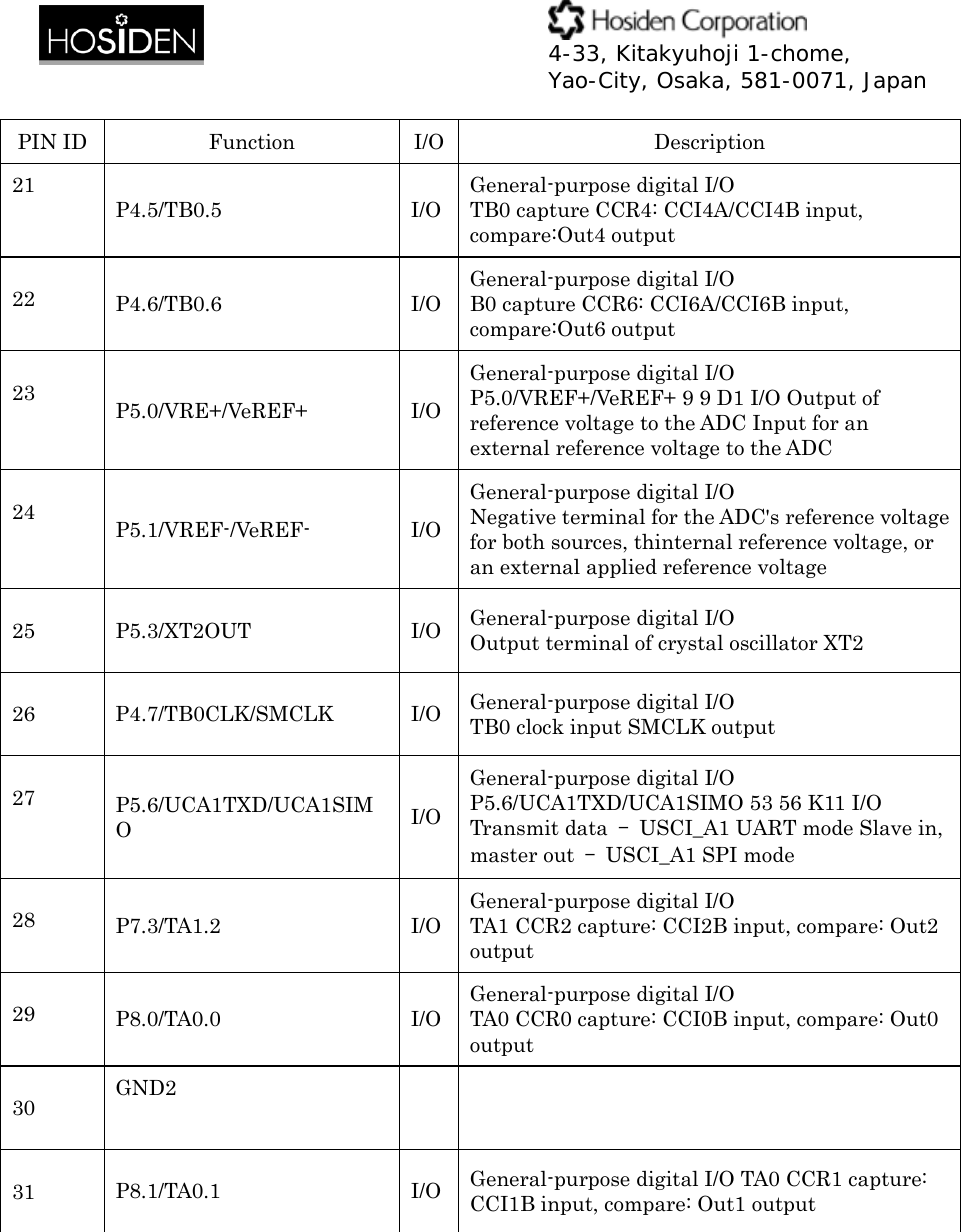
![4-33, Kitakyuhoji 1-chome, Yao-City, Osaka, 581-0071, Japan Pin Assignment and Layout CFU0321 Pin Assignments PIN ID Function I/O Description 1 GND1 2 P2.0/TA1CLK/MCLK I/O General-purpose digital I/O with port interrupt TA1 clock signal TA1CLK input MCLK output 3 P2.1/TA1.0 I/OGeneral-purpose digital I/O with port interrupt TA1 CCR0 capture: CCI0A input, compare: Out0 output 4 P2.3/TA1.2 I/OGeneral-purpose digital I/O with port interrupt TA1 CCR1 capture: CCI1A input, compare: Out1 output 5 P2.4/RTCCLK I/O General-purpose digital I/O with port interrupt RTCCLK output 6 P2.5/ROSC I/O General-purpose digital I/O with port interrupt 7 P2.6/ACLK I/O General-purpose digital I/O with port interrupt ACLK output (divided by 1, 2, 4, 8, 16, or 32) 8 P2.7/ADC12CLK/DMAE0 I/OGeneral-purpose digital I/O with port interrupt Conversion clock input ADC DMA external trigger input 9 P3.0/UCB0STE/UCA0CLK I/OGeneral-purpose digital I/O Slave transmit enable – USCI_B0 SPI mode P3.0/UCB0STE/UCA0CLK 33 35 L5 I/O Clock signal input – USCI_A0 SPI slave mode Clock signal output – USCI_A0 SPI master mode 10 P3.1/UCB0SIMO/ UCB0SDA/[FLASH_SIMO] I/OGeneral-purpose digital I/O Slave in, master out – USCI_B0 SPI mode I2C data – USCI_B0 I2C mode](https://usermanual.wiki/Hosiden/CFU0321/User-Guide-1701146-Page-6.png)
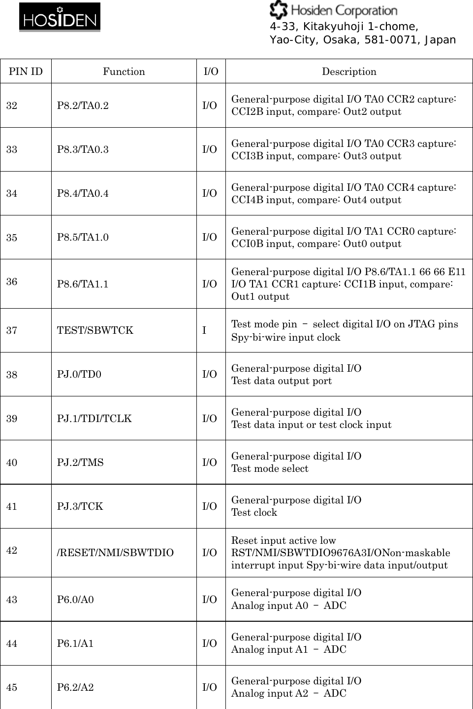
![4-33, Kitakyuhoji 1-chome, Yao-City, Osaka, 581-0071, Japan PIN ID Function I/O Description 11 P3.2/UCB0SOMI/ UCB0SCL/[FLASH_SOMI] I/OGeneral-purpose digital I/O P3.2/UCB0SOMI/UCB0SCL 35 37 J6 I/O Slave out, master in – USCI_B0 SPI mode I2C clock – USCI_B0 I2C mode 12 P3.3/UCB0CLK/UCA0STE/ [FLASH_CLK] I/OGeneral-purpose digital I/O Clock signal input – USCI_B0 SPI slave mode P3.3/UCB0CLK/UCA0STE 36 38 L6 I/O Clock signal output – USCI_B0 SPI master modeSlave transmit enable – USCI_A0 SPI mode 13 P3.4/UCA0TXD/ UCA0SIMO I/OGeneral-purpose digital I/O P3.4/UCA0TXD/UCA0SIMO 39 39 L7 I/O Transmit data – USCI_A0 UART mode Slave in, master out – USCI_A0 SPI mode 14 P3.5/UCA0RXD/ UCA0SOMI I/OGeneral-purpose digital I/O P3.5/UCA0RXD/UCA0SOMI 40 40 J7 I/O Receive data – USCI_A0 UART mode Slave out, master in – USCI_A0 SPI mode 15 P3.6/UCB1STE/UCA1CLK4120 I/OGeneral-purpose digital I/O Slave transmit enable – USCI_B1 SPI mode P3.6/UCB1STE/UCA1CLK 41 41 M8 I/O Clock signal input – USCI_A1 SPI slave mode Clock signal output – USCI_A1 SPI master mode 16 P4.0/TB0.0 I/OGeneral-purpose digital I/O TB0 capture CCR0: CCI0A/CCI0B input, compare:Out0 output 17 P4.1/TB0.1 I/OGeneral-purpose digital I/O TB0 capture CCR1: CCI1A/CCI1B input, compare:Out1 output 18 P4.2/TB0.2 I/OGeneral-purpose digital I/O TB0 capture CCR2: CCI2A/CCI2B input, compare:Out2 output 19 P4.3/TB0.3 I/OGeneral-purpose digital I/O TB0 capture CCR3: CCI3A/CCI3B input, compare:Out3 output 20 P4.4/TB0.4 I/OGeneral-purpose digital I/O TB0 capture CCR4: CCI4A/CCI4B input, compare:Out4 output](https://usermanual.wiki/Hosiden/CFU0321/User-Guide-1701146-Page-7.png)