Hp Computer Accessories 6269B Users Manual TM 11 6625 2958 14&P
6269b to the manual 1967ec14-931b-423a-9ba2-ca8e47a5b501
2015-02-09
: Hp Hp-Computer-Accessories-6269B-Users-Manual-545555 hp-computer-accessories-6269b-users-manual-545555 hp pdf
Open the PDF directly: View PDF ![]() .
.
Page Count: 96
- TOC
- LOI
- LOT
- WARNING
- SECTIONS
- SECTION 0
- SECTION I
- SECTION II
- SECTION III
- SECTION IV
- SECTION V
- PARA 5-1
- PARA 5-3
- PARA 5-5
- PARA 5-7
- PARA 5-11
- PARA 5-13
- PARA 5-15
- PARA 5-27
- PARA 5-32
- PARA 5-40
- PARA 5-44
- PARA 5-51
- PARA 5-56
- PARA 5-62
- PARA 5-64
- PARA 5-65
- PARA 5-67
- PARA 5-68
- PARA 5-71
- PARA 5-73
- PARA 5-75
- PARA 5-77
- PARA 5-79
- PARA 5-81
- PARA 5-83
- PARA 5-84
- PARA 5-85
- PARA 5-86
- PARA 5-88
- PARA 5-89
- PARA 5-90
- PARA 5-92
- PARA 5-93
- PARA 5-94
- PARA 5-95
- PARA 5-97
- PARA 5-98
- PARA 5-99
- PARA 5-101
- PARA 5-103
- PARA 5-105
- PARA 5-107
- PARA 5-109
- PARA 5-111
- SECTION VI
- SECTION VII
- FIGURES
- FIGURE 1-1
- FIGURE 2-1
- FIGURE 2-2
- FIGURE 2-3
- FIGURE 2-4
- FIGURE 2-5
- FIGURE 3-1
- FIGURE 3-2
- FIGURE 3-3
- FIGURE 3-4
- FIGURE 3-5
- FIGURE 3-6
- FIGURE 3-7
- FIGURE 3-8
- FIGURE 3-9
- FIGURE 3-10
- FIGURE 3-11
- FIGURE 3-12
- FIGURE 4-1
- FIGURE 4-2
- FIGURE 4-3
- FIGURE 4-4
- FIGURE 5-1
- FIGURE 5-2
- FIGURE 5-3
- FIGURE 5-4
- FIGURE 5-5
- FIGURE 5-6
- FIGURE 5-7
- FIGURE 5-8
- FIGURE 5-9
- FIGURE 5-10
- FIGURE 7-1
- FIGURE 7-2
- FIGURE 7-3
- FIGURE 7-4
- FIGURE 7-5
- FIGURE 7-6
- FIGURE 7-7
- FIGURE 7-8
- FIGURE 7-9
- FIGURE 7-10
- FIGURE 7-11
- TABLES
- APPENDICES
- PAGES
- PAGE 0-1
- PAGE 1-1
- PAGE 1-2
- PAGE 1-3
- PAGE 2-1
- PAGE 2-2
- PAGE 2-3
- PAGE 2-4
- PAGE 3-1
- PAGE 3-2
- PAGE 3-3
- PAGE 3-4
- PAGE 3-5
- PAGE 3-6
- PAGE 3-7
- PAGE 3-8
- PAGE 3-9
- PAGE 4-1
- PAGE 4-2
- PAGE 4-3
- PAGE 4-4
- PAGE 4-5
- PAGE 4-6
- PAGE 4-7
- PAGE 4-8
- PAGE 5-1
- PAGE 5-2
- PAGE 5-3
- PAGE 5-4
- PAGE 5-5
- PAGE 5-6
- PAGE 5-7
- PAGE 5-8
- PAGE 5-9
- PAGE 5-10
- PAGE 5-12
- PAGE 5-13
- PAGE 5-14
- PAGE 5-15
- PAGE 5-16
- PAGE 5-17
- PAGE 5-18
- PAGE 5-19
- PAGE 5-20
- PAGE 5-21
- PAGE 5-22
- PAGE 6-1
- PAGE 6-2
- PAGE 6-5
- PAGE 6-12
- PAGE 7-1
- PAGE 7-2
- PAGE 7-3
- PAGE 7-4
- PAGE 7-5
- PAGE 7-6
- PAGE 7-7
- PAGE A-1
- PAGE B-1
- PAGE B-2
- PAGE D-1
- PAGE D-3
- PAGE D-4
- PAGE D-5

SAFETY STEPS TO FOLLOW IF SOMEONE
IS THE VICTIM OF ELECTRICAL SHOCK
DO NOT TRY TO PULL OR GRAB THE INDIVIDUAL
IF POSSIBLE , TURN OFF THE ELECTRICAL POWER
IF YOU CANNOT TURN OFF THE ELECTRICAL
POWER, PULL, PUSH, OR LIFT THE PERSON TO
SAFETY USING A WOODEN POLE OR A ROPE OR
SOME OTHER INSULATING MATERIAL
SEND FOR HELP AS SOON AS POSSIBLE
AFTER THE INJURED PERSON IS FREE OF
CONTACT WITH THE SOURCE OF ELECTRICAL
SHOCK, MOVE THE PERSON A SHORT DISTANCE
AWAY AND IMMEDIATELY START ARTIFICIAL
RESUSCITATION

This manual includes copyright material reproduced by permission of the HEWLETT-PACKARD Company.
TM 11-6625-2958-14&P
TECHNICAL MANUAL
HEADQUARTERS
DEPARTMENT OF THE ARMY
No. 11-6625-2958-14&P Washington DC, 21 August 1980
OPERATOR’S, ORGANIZATIONAL, DIRECT SUPPORT AND
GENERAL SUPPORT MAINTENANCE MANUAL
(INCLUDING REPAIR PARTS AND SPECIAL TOOLS LISTS)
FOR
DC POWER SUPPLY PP-7545/U
(HEWLETT-PACKARD MODEL 6269B)
(NSN 6130-00-148-1796)
FOR SERIALS 1027A00101 AND ABOVE*
REPORTING OF ERRORS
You can improve this manual by recommending improvements using DA Form 2028-2 located
in the back of the manual. Simply tear out the self-addressed form, fill it out as shown on the sam-
ple, fold it where shown, and drop it in the mail.
If there are no blank DA Forms 2028-2 in the back of your manual, use the standard DA Form
2028 (Recommended Changes to Publications and Blank Forms) and forward to Commander, US
Army Communications and Electronics Materiel Readiness Command, ATTN: DRSEL-ME-MQ,
Fort Monmouth, NJ 07703.
In either case a reply will be forwarded direct to yOU.
This manual is an authentication of the manufacturer's commercial literature which, through usage, has been found to cover the
data required to operate and maintain this equipment. Since the manual was not prepared0 in accordance with military specifications
and AR 310-3, the format has not been structured to consider Ievels of maintenance.
i
TABLE OF CONTENTS
Section
Page No.
Section
0
INSTRUCTIONS
. . . . . . . . . . . . . . . 6-1
0-1 Scope0-1
0-2 Indexes of Publications
0-3 Forms and Records 0-1
0-4 Reporting Equipment Im-
provement Recom-
mendations (EIR) 0-1
0-5 Administrative Storage
0-6 Destruction of Army
Electronics Materiel 0-1
IGENERAL INFORMATION. . . . . . . . 1-1
1-1 Description 1-1
1-7 Specifications 1-2
1-9 Options 1-2
1-11 Instrument/Manual
Identification 1-2
1-14 Ordering Additional Manuals 1-3
II INSTALLATION . . . . . . . . 2-1
2-1
2-3
2-5
2-7
2-9
2-11
2-13
2-15
2-17
2-19
2-21
2-23
2-25
2-27
2-29
Initial Inspection
Mechanical Check
Electrical Check
Installation Data
Location
Outline Diagram
Rack Mounting
Input Power Requirements
Connections for 208 Volt
Operation (Model 6259B,
6261B, or 6268B)
Connections for 208 Volt
Operation (Model 6260B
and 6269B)
Connections for 115 Volt
Operation (Model 6259B,
6261B, and 6268B)
Connections for 115 Volt
Operation (Model 6260B)
Connections for 50Hz
Operation
Power Cable
Repackaging for Shipment
2-1
2-1
2-1
2-1
2-1
2-1
2-1
2-1
2-1
2-2
2-3
2-3
2-4
2-4
2-4
III OPERATING INSTRUCTIONS . . . . . . . .3-1
3-1 Turn-On Checkout Procecdure 3-1
3-3 Operating Modes
3-5 Normal Operating Mode
3-7 Constant Voltage
3-9 Constant Current
3-11 Overvoltage Trip
Point Adjustment
3-14 Connecting Load
3-18 No Load Operation
3-20 Operation Beyond
Rated Output
3-1
3-1
3-2
3-2
3-2
3-2
3-2
3-3
3-22
3-23
3-32
3-41
3-46
3-50
3-55
3-59
3-60
3-62
3-65
3-67
Optional Operating Modes
Remote Programming,
Constant Voltage
Remote Programming,
Constant Current
Remote Sensing
Auto-Parallel Operation
Auto-Series Operation
Auto-Tracking Operation
Special Operating
Considerations
Pulse Loading
Output Capacitance
Reverse Voltage Loading
Reverse Current Loading
Page No.
3-3
3-3
3-4
3-5
3-6
3-7
3-8
3-8
3-8
3-9
3-9
3-9
IV PRINCIPLES OF OPERATION.. . . . ...4-1
4-1
4-16
4-17
4-27
4-29
4-31
4-38
4-43
4-46
4-50
4-56
4-59
4-64
4-68
Overall BIock Diagram
Discussion
Detailed Circuit Analysis
Preregulator Control Circuit
Series Regulator and Driver
Short Circuit Protection
Constant Voltage Comparator
Constant Current Comparator
Voltage Clamp Circuit
Mixer and Error Amplifiers
Overvoltage Protection
Crowbar
Turn-On Control Circuit
Reference Regulator
Meter Circuit
Additional Protection Features
4-1
4-3
4-3
4-4
4-4
4-5
4-5
4-6
4-6
4-6
4-7
4-7
4-7
4-8
vMAINTENANCE . . . . . . . . . . . . . . . . . .. 5-1
5-1
5-3
5-5
5-7
5-40
5-51
5-56
5-62
5-71
5-73
5-75
5-77
5-79
5-81
5-90
.5-99
Introduction
Test Equipment Required
performance Test
Constant Voltage Tests
Constant Current Tests
Troubles hooting
Overall Troubleshooting
Procedure
Disassembly Procedures
Repair and Replacement
Adjustment and Calibration
Meter Zero
Voltmeter Calibration
Ammeter Calibration
Constant Voltage
Programming Current
Constant Current
Programming Current
Transient Recovery Time
5-101 Ripple Imbalance 150 and
60Hz Operation)
iii
5-l
5-1
5-2
5-2
5-7
5-9
5-10
5-15
5-16
5-18
5-18
5-18
5-18
5-19
5-20
5-20
5-20
0-1
0-1

TABLE OF CONTENTS (Continued)
SectionPage No. Section
V MAINTANCE . . Continued Page No.
5-111 Crowbar Disablement 5-22
5-103 Preregulator Tracking (5 O and
60Hz Operation) 5-21 VI REPLACEABLE PARTS . . . . . . . . . . . ...6-1
5-105 50Hz Operation (Option 005) 5-21 6-1 Introduction 6-1
5-107 Crowbar Trip Voltage 5-21 6-4 Ordering Information 6-1
5-109 Maximum Crowbar
Trip Voltage 5-22 VII CIRCUIT DIAGRAMS & COMPONENT
LOCATION DIAGRAMS . . . . . . . . . . . 7-1
APPENDIX
A.
B.
SectionI.
II.
III.
APPENDIX
c.
D.
SectionI.
II.
111.
Iv.
Table
1-1
5-1
5-2
5-3
5-4
5-5
5-6
5-7
5-8
6-1
6-2
6-3
6-4
6-5
References
Components of End Item List
Introduction
Integral Components of End Item
Basic Issue Items
Additional Authorization List (N/A)
Maintenance Allocation Chart
Introduction
Maintenance Allocation Chart
Tools and Test Equipment Required
Remarks
LIST OF TABLES
Page No.
A-1
D-1
D-1
D-3
D-4
D-5
Page No
Specifications . . . . . . . . . . . . . . . . . . . . . . . . . . . . . . . . . . . . . . . . . . . . . . . . . . . . . . . . .
1-3
Test Equipment Required . . . . . . . . . . . . . . . . . . . . . . . . . . . . . . . . . . . . . . . . . . . . . . . . 5-1
Reference and Bias Voltages. . . . . . . . . . . . . . . . . . . . . . . . . . . . . . . . . . . . . . . . . . . . . 5-10
Overall Troubleshooting . . . . . . . . . . . . . . . . . . . . . . . . . . . . . . . . . . . . . . . . . . . . . . . . 5-10
Feedback Loop Isolation . . . . . . . . . . . . . . . . . . . . . . . . . . . . . . . . . . . . . . . . . . . . . . . . 5-12
Series Regulator Troubleshooting, High Voltage Condition . . . . . . . . . . . . . . . . ...5-13
Series Regulator Troubleshooting, Low Voltage Condition. . . . . . . . . . . . . . . . . ...5-13
Preregulator Troubleshooting . . . . . . . . . . . . . . . . . . . . . . . . . . . . . . . . . . . . . . . . . . . . 5-14
Checks and Adjustments After Replacement of Semiconductor Devices . . . . . . . . .5-17
Reference Designators. . . . . . . . . . . . . . . . . . . . . . . . . . . . . . . . . . . . . . . . . . . . . . . . . . 6-1
Description Abbreviations . . . . . . . . . . . . . . . . . . . . . . . . . . . . . . . . . . . . . . . . . . . . ...6-1
Code List of Manufacturers . . . . . . . . . . . . . . . . . . . . . . . . . . . . . . . . . . . . . . . . . . . . . . 6-2
Replaceable Parts. . . . . . . . . . . . . . . . . . . . . . . . . . . . . . . . . . . . . . . . . . . . . . . . . . . . . . 6-5
Part Number-National Stock Number Cross Reference Index . . . . . . . 6-12
MANUAL CHANGES
Check the serial number of your power supply.
Then refer to the manual changes at the rear
of this technical manual and make changes as
required so that your power supply can be
correctly serviced.
iv
LIST OF ILLUSTRATIONS
Figure
Page No.
1-1 DC Power Supply, Model 6259B, 6260B, 6261B, 6268B, or 6269B . . . . . . . . . . . .. l-l
2-1 Outline Diagram . . . . . . . . . . .. . . . . . . . . . . . . . . . . . . . . . . . . . . . . . . . . . . . . . . . . . . . 2-1
2-2 Bias Transformer Primary Connections for 208Vac and 115Vac Operation . . . . . . .2-2
2-3 Power Transformer Primary Connections for 208Vac and 115Vac Operation . . . ...2-2
2-4 Power Transformer T1 Primary Connections for 208Vac Operation. . . . . . . . . . . . .. 2-3
2-5 RF I Choke (A2L1A/A2L1B) Connections for 115Vac Operation . . . . . . . . . . . . . . ...2-3
3-1 Front Panel Controls and Indicators . . . . . . . . . . . . . . . . . . . . . . . . . . . . . . . . . . . . . . 3-1
3-2 Normal Strapping Pattern . . . . . . . . . . . . . . . . . . . . . . . . . . . . . . . . . . . . . . . . . . . . . ...3-2
3-3 Remote Resistance Programming (Constant Voltage) . . . . . . . . . . . . . . . . . . . . . . ...3-3
3-4 Remote Voltage Programming, Unity Gain (Constant Voltage) . . . . . . . . . . . . . . ...3-3
3-5 Remote Voltage Programming, Non-Unity Gain (Constant Voltage). . . . . . . . . . ...3-4
3-6 Remote Resistance Programming (Constant Current) . . . . . . . . . . . . . . . . . . . . . . ...3-4
3-7 Remote Voltage Programming, Unity Gain (Constant Current) . . . . . . . . . . . . . . ...3-5
3-8 Remote Voltage Programming, Non-Unity Gain (Constant Current). . . . . . . . . . ...3-5
3-9 Remote Sensing. . . . . . . . . . . . . . . . . . . . . . . . . . . . . . . . . . . . . . . . . . . . . . . . . . . . . . . . 3-5
3-10 Auto-Parallel Operation, Two and Three Units . . . . . . . . . . . . . . . . . . . . . . . . . . ...3-6
3-11 Auto-Series Operation, Two and Three Units . . . . . . . . . . . . . . . . . . . . . . . . . . . . ...3-7
3-12 Auto-Tracking, Two and Three Units . . . . . . . . . . . . . . . . . . . . . . . . . . . . . . . . . . . . . . 3-8
4-1 Overall Block Diagram . . . . . . . . . . . . . . . . . . . . . . . . . . . . . . . . . . . . . . . . . . . . . . . . ...4-1
4-2 Operating Locus of a CV/CC Power Supply . . . . . . . . . . . . . . . . . . . . . . . . . . . . . . . . 4-2
4-3 Triac Phase Control Over AC Input Amplitude . . . . . . . . . . . . . . . . . . . . . . . . . . . ...4-3
4-4 Preregulator Control Circuit Waveforms . . . . . . . . . . . . . . . . . . . . . . . . . . . . . . . . . . . 4-4
5-1 Differential Voltmeter Substitute Test Setup . . . . . . . . . . . . . . . . . . . . . . . . . . . . . . . 5-2
5-2 Constant Voltage Load Regulation Test Setup . . . . . . . . . . . . . . . . . . . . . . . . . . . . . .
5-3
5-3 Ripple Test Setup . . . . . . . . . . . . . . . . . . . . . . . . . . . . . . . . . . . . . . . . . . . . . . . . . . . . . . 5-4
5-4 Noise Spike Measurement Test Setup . . . . . . . . . . . . . . . . . . . . . . . . . . . . . . . . . . ...5-5
5-5 Transient Recovery Time Test Setup . . . . . . . . . . . . . . . . . . . . . . . . . . . . . . . . . . . ...5-6
5-6 Transient Recovery Time Waveforms . . . . . . . . . . . . . . . . . . . . . . . . . . . . . . . . . . . ...5-6
5-7 Current Sampling Resistor Connections . . . . . . . . . . . . . . . . . . . . . . . . . . . . . . . . . ...5-8
5-8 Constant Current Load Regulation Test Setup . . . . . . . . . . . . . . . . . . . . . . . . . . . ...5-8
5-9 Constant Current Ripple and Noise Test Setup . . . . . . . . . . . . . . . . . . . . . . . . . . ...5-9
5-10 “ZERO ADJUST’’ Section of Main Circuit Board . . . . . . . . . . . . . . . . . . . . . . . . . . ...5-19
7-1 A2 RFI Assembly Component Location Diagram . . . . . . . . . . . . . . . . . . . . . . . . . . ...7-2
7-2 A3 Interconnection Circuit Board Assembly Component Location Diagram. . . . ...7-2
7-3 Top Front Chassis Assembly Component Location Diagram . . . . . . . . . . . . . . . . . . . . 7-3
7-4 Bottom Front Chassis Assembly Component Location Diagram . . . . . . . . . . . . . ...7-4
7-5 Bottom Rear Chassis Assembly Component Location Diagram . . . . . . . . . . . . . . ...7-5
7-6 Series Regulator Emitter Resistor Assembly Component Location Diagram . . . ...7-6
7-7 A4 Heat Sink Assembly Component Location Diagram (Top View) . . . . . . . . . . . ...7-6
7-8 A4 Heat Sink Assembly Component Location Diagram (End View) . . . . . . . . . . . ...7-7
7-9 Preregulator Control Circuit Waveforms . . . . . . . . . . . . . . . . . . . . . . . . . . . . . . . . . . . 7-7
7-10 A1 Main Printed Circuit Board Component Location Diagram. . . . . . . . . . . . . . . ...7-8
7-11 Schematic Diagram . . . . . . . . . . . . . . . . . . . . . . . . . . . . . . . . . . . . . . . . . . . . . . . . . . . . Foldout
v

TM 11-6625-2958-14&P
SECTION O
INTRODUCTION
.
0-1. SCOPE.
a. This manual describes DC Power
Supply PP-7545/U (fig. l-l) and
provides maintenance instructions.
Throughout this manual, PP-7545/U
is referred to as the Hewlett-Pack-
ard (HP) Model 6269B DC Power
supply.
0-2. INDEXES OF PUBLICATIONS.
a. DA Pam 310-4. Refer to the latest issue of
DA Pam 310-4 to determine whether there are new
editions, changes, additional publications per-
taining to the equipment.
b. DA Pam 310-7: Refer to DA Pam 310-7 to
determine whether there are modification work
orders (MWO’s) pertaining to the equipment.
0-3. FORMS AND RECORDS.
a. Reports of Maintenance and Unsatisfactory
Equipment. Maintenance forms, records, and
reports which are to be used by maintenance per-
sonnel at all maintenance levels are listed in and
preSCribed by TM 38-750.
b. Report of Packaging and Handling Deficien-
ties. FiII out and forward DD Form 6 (Packaging
Improvement Report) as prescribed in AR 735-11
-2/NAVUPINST4440.127E/AFR 400-54/MCO
4430.3E and DSAR 4140.55.
c. Discrepancy in Shipment Report (DISREP)
(SF 361). Fill out and forward Discrepancy in
Shipment Report (DISREP) (SF 361) as prescribed
in AR 55-38/NAVSUPlNST 4610.33B/AFR 75-
18\MCO P4610.19C and DLAR 4500.15.
0-4. REPORTING EQUIPMENT
IMPROVEMENT
RECOMMENDATIONS (EIR).
EIR’s will be prepared using SF 368 (Quality Defi-
ciency Report). Instructions for preparing EIR’s
are provided in TM 38-750, the Army Mainten-
ance Management System. El R’s should be mailed
direct to Commander, US Army Communication
and Electronics Materiel Readiness Command,
ATTN: DRSEL-ME-MQ, Fort Monmouth, NJ
07703. A reply will be furnished direct to you.
0-5. ADMINISTRATIVE STORAGE.
Administrative storage of equipment issued to and
used by Army activities shall be in accordance with
TM 740-90-1 and paragraph 2-8.
0-6. DESTRUCTION OF ARMY
ELECTRONICS MATERIEL.
Destruction of Army electronics materiel to pre-
vent enemy use shall be in accordance with TM
750-244-2.
SAFETY PRECAUTIONS.
A periodic review of safety precautions in TB 385-4 is
recommended. When the equipment is operated with covers
removed while performing maintenance, DO NOT TOUCH ex-
posed connections or compments. MAKE CERTAIN you are
not grounded when making connections or adjusting com-
ponents inside the power supply.
WARNING
HIGH VOLTAGE is used during the “performance
of maintenance as instructed in this manual.
DEATH ON CONTACT may result if personnel
fail to observe safety precautions.
0-1
TM 11-6625-2958-14&P
SECTION I
GENERAL INFORMATION
Figure 1-1. DC Power Supply, Model 6259B, 6260B, 6261B, 6268B, or 6269B
1-1 DESCRIPTION
1-2 This power supply, Figure 1-1, is completely
transistorized and suitable for either bench or relay
rack operation. It is a well-regulated, constant
voltage/constant current supply that will furnish
full rated output voltage at the maximum rated out-
put current or can be continuously adjusted through-
out the output range. The front panel CURRENT con-
trols can be used to establish the output current
limit (overload or short circuit) when the supply is
used as a constant voltage source and the VOLTAGE
controls can be used to establish the voltage limit
(ceiling) when the supply is used as a constant cur-
rent source. The supply will automatically cross
over from constant voltage to constant current oper-
ation and vice versa if the output current or voltage
exceeds these preset limits.
1-3 The power supply contains an added feature
for protection of delicate loads. A limit can be set
on the output voltage. If this limit is exceeded the
output will automatically be shorted.
1-4 The power supply has rear output terminals.
Either the positive or negative output terminal may
be grounded or the power supply can be operated
floating at up to a maximum of 300 volts above
ground.
1-5 Output voltage and current are continuously
monitored on two front panel meters.
1-6 TerminaIs located at the rear of the unit allow
access to various control points within the unit to
expand the operating capabilities of the power sup-
ply. A brief description of these capabilities is
given below:
a. Remote Programming. The power supply
output voltage or current may be programmed (con-
trolled) from a remote location by means of an ex-
ternal voltage source or resistarice.
b. Remote-Sensing. The degradation in regu-
lation which occurs at the load due to voltage drop
in the load leads can be reduced by using the pow-
er supply in the remote sensing mode of operation.
c. Auto-Series Operation. Power supplies
1-1

TM 11-6625-2958-14&P
may be used in series when a higher output voltage
is required in the constant voltage mode of opera-
t ion or when greater voltage compliance is required
in the constant current mode of operation. Auto-
Series operation permits one-knob control of the
total output voltage from a “master” supply.
d. Auto-Parallel Operation. The power sup-
ply may be operated in parallel with a similar unit
when greater output current capability is required.
Auto-Parallel operation permits one-knob control of
the total output current from a “master” supply.
e. Auto-Tracking. The power supply may be
used as a “master” supply controlling one or more
“slave” supplies furnishing various voltages for a
system.
1-7 SPECIFICATIONS
1-8 Detailed specifications for the power supply
are given in Table 1-1 on Page 1-3.
1-9 OPTIONS
1-10 Options are customer-requested factory mod-
ifications of a standard instrument. The following
options are available for the instrument covered by
this manual. Where necessary, detailed coverage
of the options is included throughout the manual.
Option No.
005
007
008
009
010
013
Description
50Hz Regulator Realignment: Stand-
ard instruments are designed for 57 to
63 Hz operation. Option 005 (factory
realignment) is necessary when the
instrument is to be operated from a
50Hz ac source. The option consists
of changing a resistor in the preregu -
lator circuit and adjusting the prereg-
ulator tracking.
Ten-Turn Output Voltage Control:
A single control that replaces the
coarse voltage control and allows
greater resolution in setting the out-
put voltage.
Ten-Turn Output Current Control:
A single control that replaces the
coarse current control and allows
greater resolution in setting the out-
put current.
Ten-Turn Output Voltage and Current
Controls: Options 007 and 008 on the
same instrument.
Chassis Slides: Enables convenient
access to power supply interior for
maintenance purposes.
Three Digit Graduated Decadial
Voltage Control: A single control that
replaces the coarse voltage control
and allows accurate resetting of the
output voltage.
020
021
022
Option No. Description
014
Three Digit Graduated Decadial Cur-
rent Control: A single control that
replaces the coarse current control
and allows accurate resetting of the
output current.
Rewire for 115Vac Input (6260B only):
Consists of replacing the input power
transformer and circuit breaker, and
reconnecting the bias transformer, RFI
choke, and fans for 115Vac operation.
Voltage Programming Adjustment:
Two rear panel mounted, screwdriver-
adjustable controls that allow accu-
rately setting the zero volt output and
the constant voltage programming co-
efficient.
Current Programming Adjustment:
Two rear panel mounted, screwdriver-
adjustable controls that allow accu-
rately setting the zero current output
and the constant current programming
coefficient.
Voltage and Current Programming
Adjustments: Options 020 and 021 on
the same instrument.
Rewire for 115Vac Input (6259B,
6261B, and 6268B only): Consists of
replacing the line circuit breaker, and
reconnecting the input power transfor-
mer, bias transformer, RF I choke, and
fans for 115Vac operation.
Rewire for 208Vac Input: Consists
of reconnecting the input power trans-
former and bias transformer for 208V
ac operation.
027
1-11 lNSTRUMENT/MANUAL IDENTIFICATION
1-12 Hewlett-Packard power supplies are identified
by a two-part serial number. The first part is the
serial number prefix, a number-letter combination
that denotes the date of a significant design change
and the country of manufacture. The first two digits
indicate the year (10= 1970, 11= 1971, etc.), the
second two digits indicate the week, and the letter
“A” designates the U.S.A. as the country of manu-
facture. The second part is the power supply serial
number;
a different sequential number is assigned
to each power supply, starting with 00101.
1-13 If the serial number on your instrument does
not agree with those on the title page of the manual,
Change Sheets supplied with the manual or Manual
Backdating Changes in Appendix A define the dif-
ferences between your instrument and the instru-
ment described by this manual.
1-2

TM 11-6625-2958-14&P
1-14 ORDERING ADDITIONAL MANUALS
your local Hewlett-Packard field office (see list at
rear of this manual for addresses). Specify the
1-15 One manual is shipped with each power sup- model number, serial number prefix, and HP part
ply. Additional manuals may be purchased from number shown on the title page.
Table 1-1. Specifications
INPUT:
230Vac *10%, single phase, 57-63 Hz, 18A,
2500W @ 230V.
OUTPUT :
0-40 volts @ 0-50 amperes.
LOAD REGULATION:
Constant Voltage - Less than 0.01% plus 200µV
for a load current change equal to the current
rating of the supply.
Constant Current - Less than 0.02% plus 2mA
for a load voltage change equal to the voltage
rating of the supply.
LINE REGULATION :
Constant Voltage - Less than 0.01% plus 200µV
for a change in line voltage from 207 to 253 volts
at any output voltage and current within rating.
Constant Current - Less than 0.02% plus 2mA
for a change in line voltage from 207 to 253 volts
at any output voltage and current within rating.
RIPPLE AND NOISE:
Constant Voltage - Less than 1mV rms, 5mV
P-P (dc to 20MHz).
Constant Current - Less than 25mA rms.
TEMPERATURE RATINGS:
Operating: O to 55°C. Storage: -40 to +75°C.
TEMPERATURE COEFFICIENT:
Constant Voltage - Less than O .01% plus 200µV
change in output per degree Centigrade change in
ambient following 30 minutes warm-up.
Constant Current - Less than 0.01% plus 4mA
change in output per degree Centigrade change in
ambient following 30 minutes warm-up.
STABILITY :
Constant Voltage - Less than O .03% plus 2mV
total drift for 8 hours following 30 minutes warm-
up under constant ambient conditions.
Constant Current- Less than 0.03% plus 10mA
total drift for 8 hours following 30 minutes warm-
up under constant ambient conditions.
TRANSIENT RECOVERY TIME:
Less than 50µsec is required for output voltage
recovery (in constant voltage operation) to within
10mV of the nominal output voltage following a
S ampere change in output current.
METERS:
A front panel voltmeter (0-50V) and ammeter
(0-60A) is provided. (Accurate within 2% of full
scale. )
OUTPUT CONTROLS:
Single-turn coarse and fine voltage and current
controls are included on the front panel.
OUTPUT TERMINALS:
Output bus bars are located on the rear of the
chassis. Both bus bars are isolated from the
chassis and either the positive or negative bus
bar may be connected to the chassis through a
separate, adjacent ground terminal.
REMOTE VOLTAGE PROGRAMMING:
All programming terminals are on a rear
barrier strip.
Constant Voltage - 1V/volt (accuracy: 1%).
Constant Current - 10mV/amp (Accuracy 10%).
REMOTE RESISTANCE PROGRAMMING:
All programming terminals are on a rear
barrier strip.
Constant Voltage -200 ohms/volt (Accuracy:
1%).
Constant Current -4 ohms/ampere (Accuracy
10%).
OVERVOLTAGE PROTECTION CROWBAR:
The minimum crowbar trip setting above the
desired operating output voltage” to prevent false
crowbar tripping is 5% of output voltage setting
plus 2 volts. Range is 4 to 45Vdc.
COOLING:
Forced air cooling is employed. The supply has
two cooling fans.
WEIGHT:
95 lbs. (43.0 kg.) net. 120 lbs. (54.5 kg.)
shipping.
SIZE:
7.0“ (17.8cm) H x 17.511 (44.4cm) D x 19.0”
(48, 3 cm) W. The unit can be mounted in a
standard 19” rack panel.
FINISH:
Light gray front panel with dark gray case.
1-3
SECTION II
INSTALLATION
TM 11-6625-2958-14&P
2-1 INITIAL INSPECTION
2-2 Before shipment, this instrument was inspect-
ed and found to be free of mechanical and electri-
cal defects. As soon as the instrument is unpacked,
inspect for any damage that may have occurred in
transit. Save all packing materials until the in-
spection is completed. If damage is found, file a
claim with the carrier immediately. Hewlett-
Packard Sales and Service office should be notified.
2-3
MECHANICAL CHECK
2-4 This check should confirm that there are no
broken knobs or connectors, that the cabinet and
panel surfaces are free of dents and scratches,
and that the meters are not scratched or cracked.
2-5 ELECTRICAL CHECK
2-6 The instrument should be checked against
its electrical specifications. Section V includes
a n “in-cabinet” performance check to verify proper
instrument operation.
2-7 INSTALLATION DATA
2-8 The instrument is shipped ready for bench
operation. It is necessary only to connect the in-
strument to a source of power and it is ready for
operation.
.
2-9
LOCATION
2-10 This instrument is fan cooled. Sufficient
space should be allotted so that a free flow of
cooling air can reach the sides of the instrument
when it is in operation. It should be used in an
area where the ambient temperature does not ex-
ceed 55°C.
2-11 OUTLINE DIAGRAM
2-12 Figure 2-1 illustrates the outline shape and
dimensions of Models 6259B, 6260B, 6261B, 6268B,
and 6269B.
2-13 RACK MOUNTING
2-14 This instrument is full rack size and can be
easily rack mounted in a conventional 19 inch rack
panel using standard mounting screws,
Figure 2-1. Outline Diagram
2-15 INPUT POWER REQUIREMENTS
2-16 Model 6259B, 6260B, 6261B, or 6268B power
supply may be operated continuously from either a
nominal 230 volt, 208 volt, or 115 volt 57-63Hz
power source. Model 6269B may be operated from
a 230 volt or 208 volt, 57-63Hz power source only.
The instrument as shipped from the factory is wired
for 230 volt operation. The input power when oper-
ated from a 230 volt power source at full load is:
Model Input Current Input Power
6259B
6A
850W
6260B
12A
1600W
6261B
11A
1500W
6268B
11A
1600W
6269B
18A
2500W
2-17 CONNECTIONS FOR 208 VOLT OPERATION
(Model 6259B, 6261B, or 6268B: Option 027)
2-18 To convert Model 6259B, 6261B, or 6268B to
operation from a 208Vac source, taps on the power
and bias transformers must be changed as follows:
a. Remove RFI assembly as described in
Steps (a) through (c) of Paragraph 5-67. Access is
now provided to bias transformer A3T2. (See Figure
7-2.)
2-1
Figure 2-2. Bias Transformer Primary Connections
for 208Vac Operation (Model 6259B, 6260B, 6261B,
6268B, and 6269B) and 115Vac Operation
(Except Model 6269B)
b. Unsolder wire from circuit breaker A5CB1
connected to "230V" terminal of bias transformer
A3T2 and solder it instead to "208V" terminal of
transformer (see Figure 2-2 B). Leave wire from fan
B2 (not used in 62599) soldered to “230V” terminal.
c. Re-install RFI assembly by reversing pro-
cedure of Step (a).
d. Unsolder wire connected to terminal 5 of
power transformer T1 (see Figure 7-4) and solder it
instead to terminal 4 of transformer (see Figure
2-3 B).
Figure 2-3. Power Transformer Primary
Connections for 208Vac and 115Vac Operation
. (Model 6259B, 6261B, and 6268B)
2-19 CONNECTIONS FOR 208 VOLT OPERATION
(Model 6260B and 6269B: Option 027)
2-20 To convert Model 6260B or 6269B to operation
from a 208Vac source, taps on the power and bias
transformers must be changed as follows:
a. Perform Steps (a) through (c) of Paragraph
2-18. b. Unsolder wire connected to to "230V” terminal
2-2
TM 11-6625-2958-14&P
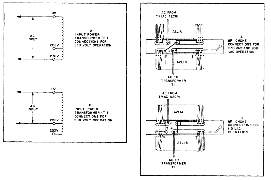
Figure 2-4. Power Transformer T 1 Primary
Connections for 208Vac Operation
(Model 6260B and 6269B)
of power transformer T1 (see Figure 7-4) and solder
it instead to "208V" terminal of transformer (see
Figure 2-4 B).
2-21 CONNECTIONS FOR 115 VOLT OPERATION
(Model -6259B, 6261B, and 6268B: Option 026)
2-22 To convert Model 6259B, 6261B, or 6268B to
operation from a 115Vac source, a new circuit
breaker must be installed and taps must be changed
on the bias transformer, power transformer, and RFI
choke as follows:
a. Obtain and install new LINE circuit
breaker (A5CB1). Connections to new circuit
breaker are same as old connections. Refer to
Option 026 in Table 6-4 (Replaceable Parts) for
current rating and HP Part Number.
b. Remove and partially disassemble RFI
assembly as described in Steps (a) through (d) of
Paragraph 5-67.
c. Unsolder jumper between terminals 2 and
3 of RFI choke mounting board and solder jumpers
between terminals 1 and 3, 2 and 4 (see Figure
2-5 B). Replace cover on RFI assembly.
d. Unsolder wires from circuit breaker
A5CB1 and fan B2 connected to "230V" terminal of
bias transformer A3T2 (see Figure 7-2). Solder
wire from circuit breaker to "115V" terminal of
transformer, and solder wire from fan to "0V" ter-
minal of transformer (see Figure 2-2 C). Note that
Figure 2-5. RFI Choke (A2L1A/A2L1B)
Connections for 115Vac Operation
(Model 6259B, 6260B, 6261B, and 6268B)
fan B2 is not used in Model 6259B.
e. Re-install RFI assembly by reversing pro-
cedure of Step (b).
f. Unsolder jumper connecting terminals 2
and 3 of power transformer T1 (see Figure 7-4) and
solder jumpers between terminals 1 and 3, 2 and 5
(see Figure 2-3 C).
2-23 CONNECTIONS FOR 115 VOLT OPERATION
(Model 6260B: Option 016)
2-24 To convert Model 6260B to operation from a
115Vac source, a new power transformer and circuit
breaker must be installed and taps must be changed
on the RFI choke and bias transformer as follows:
a. Obtain and install new power transformer
(T1) and new circuit breaker (A5CB1). Refer to
Option 016 in Table 6-4 (Replaceable Parts) for
power ratings and HP Part Numbers. New transfor-
mer has two primary terminals. Transfer wire from
old transformer "0V" terminal to new transformer
"0V" terminal, and wire from old transformer "230V"
terminal to new transformer "115V" terminal. New
circuit breaker connections are same as old.
2-3
TM 11-6625-2958-14&P
TM 11-6625-2958-14&P
b. Perform Steps (b) through (e) of Paragraph
2-22.
2-25 CONNECTIONS FOR 50Hz OPERATION
2-26 For operation from a 50Hz ac input, R82
must be replaced with a 240 Ω, ±5%, ½ watt resistor
as specified under Option 005 in Table 6-4 (Re-
placeable Parts). In addition, it is necessary to
readjust the voltage drop across the series regula-
tor (“Preregulator Tracking” , Paragraph 5-103) and
to check the ripple imbalance as described in Steps
(a) through (e) of Paragraph 5-101.
2-27 POWER CABLE
2-28 A power cable is not supplied with the in-
strument. It is recommended that the user-supplied
power cable have three conductors (third conductor
grounded) and be of sufficient wire size to handle
the input current drawn by the supply (see Paragraph
2-16). Note that when the supply is operated from
a 115Vac source, the input current is approximately
double that shown in Paragraph 2-16.
2-29 REPACKAGING FOR SHIPMENT
2-30 To insure safe shipment of the instrument, it
is recommended that the package designed for the
instrument be used. The original packaging materi-
al is reusable. If it is not available, contact your
local Hewlett-Packard field office to obtain the
materials. This office will also furnish the address
of the nearest service center to which the instru-
ment can be shipped. Be sure to attach a tag to the
instrument specifying the owner, model number,
full serial number, and service required, or a brief
description of the trouble.
2-4
TM 11-6625-2958-14&P
SECTION Ill
OPERATING INSTRUCTIONS
Figure 3-1. Front Panel Controls and Indicators,’ Modal 6259B, 6260B, 6261B, 6268B or 6269B
3-1 TURN-ON CHECKOUT PROCEDURE 3-3 OPERATING MODES
3-2 The following checkout procedure describes
the use of the front panal controls and indicators
(Figure 3-1) and ensures that the supply is opera-
tional.a. Set LINE circuit breaker ① to ON, and
observe that pilot light ② lights.
b. Adjust VOLTAGE controls ③ until desired
voltage is indicated on voltmeter ④ .
c. To ensure that overvoltage crowbar cir-
cuit is operational, rotate OVERVOLTAGE ADJUST
control ⑤ (screwdriver adjust) counterclockwise
until unit crowbars. Overvoltage lamp ⑥ will
light and output voltage will fall to zero volts.
d. To deactivate crowbar, return OVERVOLT-
AGE ADJUST control to its maximum clockwise po-
sition and turn off supply. Turn supply back on
and voltage should again be value obtained in step
(b).
e. To check out constant current circuit,
turn off supply. Short circuit rear output terminals
and turn on supply.
f. Adjust CURRENT controls ⑦ until desired
output current is indicated on ammeter ⑧ .
g. Remove short circuit and read following
paragraphs before connecting actual load to supply.
3-4 The power supply is designed so that its mode
of operation can be selected by making strapping
connections between particular terminals on the ter-
minal strip at the rear of the power supply. The ter-
minal designations are stenciled in white on the
power supply below their respective terminals. The
following paragraphs describe the procedures for
utilizing the various operational capabilities of the
power supply. A more theoretical description con-
cerning the operational features of this supply is
contained in Application Note 90, Power Supply
Handbook (available at no charge from your local
Hewlett-Packard sales office). Sales office ad-
dresses appear at the rear of the manual.
3-5 NORMAL OPERATING MODE
3-6 The power supply is normally shipped with
its rear terminal strapping connections arranged for
constant voltage/constant current, local sensing,
local programming, single unit mode of operation.
This strapping pattern is illustrated In Figure 3-2.
The operator selects either a constant voltage or a
constant current output using the front panel con-
trols (local programming; no strapping changes are
necessary).
3-1
TM 11-6625-2958-14&P
Figure 3-2. Normal Strapping Pattern
3-7 CONSTANT VOLTAGE
3-8 To select a constant voltage output, proceed
as follows:
a. Turn on power supply and adjust VOLTAGE
controls for desired output voltage with output ter-
minals open.
b. Short circuit output terminals and adjust
CURRENT controls for maximum output current al-
lowable (current limit), as determined by load con-
ditions. If a load change causes the current limit
to be exceeded, the power supply will automatical-
ly cross over to constant current output at the pre-
set current limit and the output voltage will drop
proportionately. In setting the current Iimit, al-
lowance must be made for high peak currents which
can cause unwanted crossover. (Refer to Paragraph
3-60. )
3-9 CONSTANT CURRENT
3-10 To select a constant current output, proceed
as follows:
a. Short circuit output terminals and adjust
CURRENT controls for desired output current.
b. Open output terminals and adjust VOLT-
AGE controls for maximum output voltage allowable
(voltage limit ), as determined by load conditions.
If a load change causes the voltage limit to be ex-
ceeded, the power supply will automatically cross
over to constant voltage output at the preset volt-
age limit and the output current will drop propor-
tionately. In setting the voltage limit, allowance
must be made for high peak voltages which can
cause unwanted crossover. (Refer to Paragraph 3-60.)
3-11 OVERVOLTAGE TRIP POINT ADJUSTMENT
3-12 The crowbar trip voltage can be adjusted by
using the screwdriver control on the front panel.
The trip voltage range is as follows:
6259B, 6260B
2 to 12Vdc 2 to 23Vdc 4 to 45Vdc
When the crowbar trips, the output is shorted and
the amber indicator on the front panel lights.
Clockwise rotation of the control produces higher
trip voltages. The factory sets the control fully
clockwise. The crowbar may be disabled complete-
ly if desired. (Refer to Paragraph 5-11 1.)
3-13 False crowbar tripping must be considered
when adjusting the trip point. If the trip voltage is
set too close to the operating output voltage of the
supply, a transient in the output will falsely trip
the crowbar. It is recommended that the crowbar be
set higher than the output voltage by 5% of the out-
put voltage plus 2 volts. However, If occasional
crowbar tripping on unloading can be tolerated, the
crowbar trip point can be set much closer to the
operating out put voltage of the supply.
3-14 CONNECTING LOAD
3-15 Each load should be connected to the power
supply output terminals using separate pairs of
connecting wires. This will minimize mutual cou-
pling effects between loads and will retain full ad-
vantage of the low output impedance of the power
supply. Each pair of connecting wires should be as
short as possible and twisted or shielded to reduce
noise pickup. (If a shielded pair is used, connect
one end of the shield to ground at the power supply
and leave the other end unconnected.)
3-16 If load considerations require that the output
power distribution terminals be remotely located
from the power supply, then the power suppIy out-
put terminals should be connected to the remote
distribution terminals via a pair of twisted or
shielded wires and each load should be separately
connected to the remote distribution terminals. For
this case, remote sensing should be used. (Refer
to Paragraph 3-4 1.)
3-17 Positive or negative voltages can be obtained
from this supply by grounding either one of. the out-
put terminals or one end of the load. Always use
two leads to connect the load to the supply, regard-
less of where the setup is grounded. This will elim-
inate any possibility of output current return paths
through the power source ground which would dam-
age the line cord plug. This supply can also be
operated up to 300Vdc above ground, if neither out-
put terminal is grounded.
3-18 NO LOAD OPERATION
3-19 When the supply is operated without a load,
down-programming speed is considerably slower
than in normal loaded operation. This slower pro-
gramming speed is evident when using any method
of down-programming - either turning the VOLTAGE
controls fully counterclockwise, activating the
crowbar, or throwing the LINE circuit breaker to
OFF. Under any of these conditions, the supply
output will rapidly fall to approximately two volts,
3-2
6261B6268B, 6269B
then proceed at a slower rate towards zero. The
actual time required for the output to fall from two
volts to zero will vary from several seconds to
several minutes, depending upon which down-pro-
gramming method is used.
3-20 OPERATION BEYOND RATED OUTPUT
3-21 The shaded area on the front panel meter face
indicates the approximate amount of output voltage
or current that may be available in excess of the
normal rated output. Although the supply can be
operated in this shaded region without being dam-
aged, it cannot be guaranteed to meet all of its
performance specifications.
3-22 OPTIONAL OPERATING MODES
3-23 REMOTE PROGRAMMING, CONSTANT
VOLTAGE
3-24 The constant voltage output of the power
supply can be programmed (controlled) from a re-
mote location if required. Either a resistance or
voltage source can be used as the programming
device. The wires connecting the programming
terminals of the supply to the remote programming
device should be twisted or shielded to reduce
noise pickup. The VOLTAGE controls on the front
panel are automatically disabled in the following
procedures.
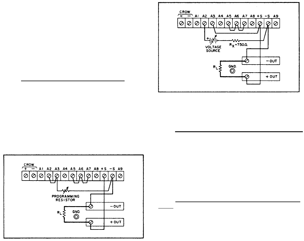
3-25 Resistance Programming (Figure 3-3). In this
mode, the output voltage will vary at a rate deter-
mined by the voltage programming coefficient of
200 ohms/volt. The programming coefficient is de-
termined by the programming current. This current
is factory adjusted to within 1% of 5mA. If greater
programming accuracy is required, it may be
achieved by either adjusting R3 as discussed in
Paragraph 5-88, or, if the instrument is equipped
with Option 020, by adjusting potentiometer R112
as discussed in Paragraph 5-89.
Figure 3-3.
Remet e Resistance Programming
(Constant Voltage)
TM 11-6625-2958-14&P
3-26 The output voltage of the supply should be
-15mV ±5mV when zero ohms is connected across
the programming terminals. If a zero ohm voltage
closer to zero than this is required, it may be
achieved by inserting and adjusting R110 as dis-
cussed in Paragraph 5-83, or, if the instrument is
equipped with Option 020, by adjusting potentiome-
ter R113 as discussed in Paragraph 5-85.
3-27 To maintain the stability and temperature co-
efficient of the power supply, use programming re-
sistors that have stable, low noise, and low temp-
erature coefficient (less than 30ppm per degree
Centigrade) characteristics. A switch can be used
in conjunction with various resistance values in
order to obtain discrete output voltages. The switch
should have make-before-break contacts to avoid
momentarily opening the programming terminals dur-
ing the switching interval.
Figure 3-4.
Remet e Voltage Programming,
Unity Gain (Constant Voltage)
3-28 Voltage Programming, Unity Gain (Figure 3-4).
Employ the strapping pattern shown in Figure 3-4
for voltage programming with unity gain. In this
mode, the output voltage will vary in a 1 to 1 ratio
with the programming voltage (reference voltage)
and the load on the programming voltage source will
not exceed 20 microampere. Impedance matching
resistor (Rx) is required to maintain the temperature
coefficient and stability specifications of the sup-
ply .
3-29 Voltage Programming, Non-Unity Gain (Figure
3-5). The strapping pattern shown in Figure 3-5
can be utilized for programming the power supply
using an external voltage source with a variable
voltage gain. The output voltage in this configura-
tion is found by multiplying the external voltage
source by (Rp/RR).
3-30 External resistors Rp and RR should have sta-
ble, low noise, and low temperature coefficient
3-3
TM 11-6625-2958-14&P
Figure 3-5. Remote Voltage Programming,
Non-Unity Gain (Constant Voltage)
(less than 30ppm Per degree Centigrade) character-
istics in order to maintain the Supply's temperature
and stability specifications. Reference resistor RR
should not exceed 10K. Note that it is possible to
use the front panel voltage control already in the
supply (A5R121) as the voltage gain control (Rp) by
simply removing the external Rp and strapping ter-
minals Al and A2 together.
3-31 The output voltage of the supply may be ad-
justed to exactly zero when the external program-
ming voltage is zero by either inserting and adjust-
ing R111 as discussed in Paragraph 5-84, or, if the
instrument is equipped with Option 020, by adjust-
ing potentiometer R112 as discussed in Paragraph
5-86.
3-32 REMOTE PROGRAMMING, CONSTANT
CURRENT
3-33 Either a resistance or a voltage source can
be used to control the constant current output of
the supply. The CURRENT controls on the front
panel are automatically disabled in the following
procedures.
3-34 Resistance Programming (Figure 3-6). In this
mode, the output current varies at a rate determined
by the programming coefficient as follows:
Model Programming Coefficient
6259B
4 ohms/ampere
6260B
2 ohms/ampere
6261B
4 ohms/ampere
6268B
6 ohms/ampere
6269B
4 ohms/ampere
The programming coefficient is determined by the
constant current programming current which is ad-
justed to within 10% of 2.5mA at the factory. If
greater programming accuracy is required, it may
be achieved by either adjusting R30 as discussed
in Paragraph 5-97, or, if the instrument is equipped
Figure 3-6. Remote Resistance Programming
(Constant Current)
with Option 021, by adjusting potentiometer R116
as discussed in Paragraph 5-98. The output current
of the supply when zero ohms is placed across the
programming terminals may be set to exactly zero
by either inserting and adjusting R117 as discussed
in Paragraph 5-92, or, if the instrument is equipped
with Option 021, by adjusting potentiometer R119
as discussed in Paragraph 5-94.
3-35 Use stable, low noise, low temperature co-
efficient (less than 30ppm/°C) programming resis-
tors to maintain the power supply temperature coef-
ficient and stability s pacifications. A switch may
be used to set discrete values of output current. A
make-before-break type of switch should be used
since the output current will exceed the maximum
rating of the power supply if the switch contacts
open during the switching interval.
If the programming terminals (A4 and
A 6) should open at any time during the
remote resistance programming mode,
the output current will rise to a value
that may damage the power supply
and/or the load. If, in the particular
programming configuration in use,
there is a chance that the terminals
might become open, it is suggested
that a 200 ohm resistor be connected
across the programming terminals.
Like the programming resistor, this
resistor should be a low noise, low
temperature coefficient type. Not e
that when this resistor is used, the
resistance value actually programming
the supply is the parallel combination
of the remote programming resistance
and the resistor across the program-
ming terminals.
3-4
CAUTION
Figure 3-7. Remote Voltage Programming,
Unity Gain (Constant Current]
3-36 Voltage Programming, Unity Gain (Figure 3-7).
In this mode, the output current will vary linearly
with changes in the programming voltage. The pro-
gramming voltage should not exceed 0.6 volts.
Voltage in excess of 0.6 volts will result in exces-
sive power dissipation in the instrument and possi-
ble damage.
3-37 The output current varies at a rate determined
by the programming coefficient as follows:
Model Programming Coefficient
6259B
10.0mV/ampere
6260B
5.0mV/ampere
6261B
10.0mV/ampere
6268B
16.7mV/ampere
6269B
10.0mV/ampere
The current required from the voltage source will be
less than 20µA. Impedance matching resistor Rx is
required to maintain the temperature coefficient and
stability specifications of the supply.
3-38 Voltage Programming, Non-Unity Gain (Figure
3-8). The power supply output current can be
Figure 3-8. Remote Voltage Programming,
Non-Unity Gain (Constant Current)
TM 11-6625-2958-14&P
programmed using an external voltage source with
variable gain by utilizing the strapping pattern
shown in Figure 3-8. In this mode, the output cur-
rent is found by multiplying the external voltage
source (Es) by [Rp/(RR x Kp)], where Kp is the
constant current voltage programming coefficient as
given in Paragraph 3-37. The value of reference
resistor RR and programming voltage source Es
should be such that the value of ES/RR is equal to
or greater than 2.5mA.
3-39 External resistors Rp and RR should have sta-
ble, low noise, and low temperature coefficient
(less than 30ppm per degree Centigrade) character-
istics in order to maintain the stability and temper-
ature specifications of the Power supply. Reference
resistor RR should not exceed 10K. Note that it is
possible to use the front panel current control al-
ready in the supply (A5R123) as the gain control (Rp)
by simply removing the external Rp and strapping
terminals AS and A6 together.
3-40 The output current of the supply may be ad-
justed to exactly zero when the external program-
ming voltage is zero by either inserting and adjust-
ing R115 as discussed in Paragraph 5-93, or, if the
instrument is equipped with Option 021, by adjust-
ing potentiometer R116 as discussed in Paragraph
5-95.
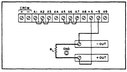
3-41 REMOTE SENSING (Figure 3-9)
3-42 Remote sensing is used to maintain good reg-
ulation at the load and reduce the degradation of
regulation which would occur due to the voltage
drop in the leads between the power supply and the
load. Remote sensing is accomplished by utilizing
the strapping pattern shown in Figure 3-9. The
Power supply should be turned off before changing
strapping paterns. The leads from the sensing (±S)
terminals to the load will carry much less current
than the load leads and it is not required that these
leads be as heavy as the load leads. However,
they must be twisted or shielded to minimize noise
pickup.
Figure 3-9. Remote Sensing
3-5
TM 11-6625-2958-14&P
3-43 For reasonable load lead lengths, remote
sensing greatly improves the performance of the
supply. However, if the load is located a consid-
erable distance from the supply, added precautions
must be observed to obtain satisfactory operation.
Notice that the voltage drop in the load leads sub-
tracts directly from the available output voltage
and also reduces the amplitude of the feedback er-
ror signals that are deveIoped within the unit. Be-
cause of these factors it is recommended that the
drop in each load lead not exceed 0.5 volt. If a
larger drop must be tolerated, please consult an
HP Sales Engineer.
NOTE
Due to the voltage drop in the load
leads, it may be necessary to read-
just the current limit in the remote
sensing mode.
3-44 Observance of the precautions in Paragraph
3-43 will result in a low dc output impedance at
the load. However, another factor that must be
considered is the inductance of long load leads.
This causes a high ac Impedance and could affect
the stability of the feedback loop seriously enough
to cause oscillation. If this is the case, it is
recommended that the following actions be taken:
a. Adjust equalization control R47 to remove
oscillation, or to achieve best possible transient
response for given long load lead configuration.
Refer to Paragraph 5-27 for discussion of transient
response measurement.
b. If performing adjustment in step (a) above
does not remove oscillation, disconnect output
capacitor A3C3 and connect a capacitor having sim-
ilar characteristics (approximately the same capa-
citance, the same voltage rating or greater, and
having good high frequency characteristics) direct-
ly across load using short leads. Readjust equali-
zation control R47 as in step (a) above after making
this change. In order to gain access to capacitor
A3C3, it is necessary to remove the RFI assembly
as described in steps (a) through (c) of Paragraph
5-67. Lead from positive side of capacitor (shown
arrowed In Figure 7-2) can then be unsoldered from
A3 interconnection circuit board.
3-45 To employ remote sensing with any method of
remote programming or with any method of combin-
ing more than one supply discussed in the Preced-
ing or following paragraphs, use the following pro-
cedure:
a. Remove the two external leads connecting
the sensing terminals (±S) to the output bus bars
(±OUT).
b. Connect a lead from the +S terminal to the
positive side of the load, and connect another lead
from the -S terminal to the negative side of the load.
Note that there may be more than one lead connect-
ed to the +S and -S terminals.
3-46 AUTO-PARALLEL OPERATION (Figure 3-10)
3-47 Two or more power supplies can be connected
in an Auto-Parallel arrangement to obtain an output
Figure 3-10. Auto-Parallel Operation,
Two and Three Units
3-6
TM 11-6625-2958-14&P
current greater than that available from one supply.
Auto-Parallel operation permits equal current shar-
ing under all load conditions, and allows complete
control of the output current from one master power
supply. The output current of each slave will be
approximately equal to the master’s output current
regardless of the load conditions. Because the
output current controls of each slave are operative,
they should be set to maximum to prevent the slave
reverting to constant current operation; this would
OCCur if the master output current setting exceeded
the slave’s.
3-48 Additional slave supplies may be added in
parallel with the master/slave combination as
shown in the bottom half of Figure 3-10. All the
connections between the master and slave #1 are
duplicated between slave #1 and the added slave
supply. In addition, the strapping pattern of the
added slave should be the same as slave #1. Re-
mote sensing and programming can be used, though
the strapping arrangements shown in Figure 3-10
show local sensing and programming.
3-49 Overvoltage protection is controlled by the
crowbar circuit in the master supply which monitors
the voltage acress the load and fires the SCR's in
both units if an overvoltage condition occurs. The
firing pulses are fed to the slave supply from trans-
former T90 (winding 5-6) of the master supply
through the “ EXT. CROWBAR TRIGGER" terminals on
the rear panel of the master supply. Correct polari-
ty must be observed in connecting the crowbars to-
gether. The overvoltage trip point is adjusted on
the master supply, The OVERVOLTAGE ADJUST po-
tentiometer on the slave supply should be set to
maximum [clockwise) so that the master crowbar
will control the slave.
3-50 AUTO-SERIES OPERATION (Figure 3-11)
3-51 Two or more power supplies can be operated
in Auto-Series to obtain a higher voltage than that
available from a single supply. When this connec-
tion is used, the output voltage of each slave sup-
ply varies in accordance with that of the master
supply. At maximum output voltage, the voltage of
the slaves is determined by the setting of the front
panel VOLTAGE controls on the master. The master
supply must be the most positive supply of the
series. The output CURRENT controls of all series
units are operative and the current limit is equal to
the lowest control setting. If any of the output
CURRENT controls are set too low, automatic cross-
over to constant current operation will occur and
the output voltage will drop. Remote sensing and
programming can be used, though the strapping ar-
rangements shown in Figure 3-11 show local sensing
and programming.
3-52 In order to maintain the temperature coeffi-
Figure 3-11. Auto-Series Operation,
Two and Three Units
cient and stability specifications of the power sup-
ply, the external resistors (Rx) shown in Figure
3-11 should be stable, low noise, low temperature
coefficient (less than 30ppm per degree Centigrade)
resistors. The value of each resistor is dependent
3-7
TM 11-6625-2958-14&P
on the maximum voltage rating of the "master" sup-
ply. The value of RX is this voltage divided by the
voltage programming current of the slave supply
(1/Kp where KP is the voltage programming coeffi-
cient). The voltage contribution of the slave is
determined by its voltage control setting.
3-53 Overvoltage protection is provided in Auto-
Series operation by connecting the crowbars in par-
allel with correct polarity as in Auto-Parallel oper-
ation (see Paragraph 3-49). The OVERVOLTAGE AD-
JUST potentiometer in each supply should be adjust-
ed so that it trips at a point slightly above the out-
put voltage that the supply will contribute.
3-54 When the center tap of an Auto-Series combi-
nation is grounded, coordinated positive and nega-
tive voltages result. This technique is commonly
referred to as “robber-banding” and an external
reference source may be employed if desired. Any
change of the internal or external reference source
(e.9. drift, ripple) will cause an equal percentage
change in the outputs of both the master and slave
supplies. This feature can be of considerable use
in analog computer and other applications, where
the load requires a positive and a negative power
supply and is less susceptible to an output voltage
change occurring simultaneously in both supplies
than to a change in either supply alone.
3-55 AUTO-TRACKING OPERATION (Figure 3-12)
3-56 The Auto-Tracking configuration is used when
several different voltages referred to a common bus
must vary in proportion to the setting of a particular
instrument (the control or master). A fraction of the
master’s output voltage is fed to the comparison
amplifier of the slave supply, thus controlling the
slave's output. The master must have the largest
output voltage of any power supply in the group. It
must be the most positive supply in the example
shown on Figure 3-12.
3-57 The output voltage of the slave (Es) is a per-
centage of the master's output voltage (EM), and is
determined by the voltage divider consisting of RX
and the voltage control of the slave supply, Rp,
where ES = EM [Rp/(Rx+Rp)]. Remote sensing and
programming can be used (each supply senses at its
own load), though the strapping patterns given in
Figure 3-12 show only local sensing and program-
ming. In order to maintain the temperature coeffi-
cient and stability specifications of the power sup-
ply, the external resistors should be stable, low
noise, low temperature coefficient (less than 30ppm
per degree Centigrade) resistors.
3-58 The overvoltage protection circuit in each
unit is operable end independently monitors the
voltage across its own load. Notice that if the
master supply crowbars, the output voltage of
Figure 3-12. Auto-Tracking, TwO and Three Units
each slave will also decrease. However, the re-
verse is not true. If one of the slave units crow-
bars, the other supplies in *the ensemble will not
be affected.
3-59 SPECIAL OPERATING CONSIDERATIONS
3-60 “PULSE LOADING
3-61 The power supply will automatically cross
3-8

over from constant voltage to constant current op-
eration, or the reverse, in response to an increase
(over the preset limit) in the output current or volt-
age, respectively. Although the preset limit may
be set higher than the average output current or
voltage, high peak currents or voltages (as occur
in pulse loading) may exceed the preset limit and
cause crossover to occur. If this crossover limit-
ing is not desired, set the preset limit for the peak
requirement and not the average.
3-62 OUTPUT CAPACITANCE
3-63 An internal capacitor (A3C3) connected across
the output terminals of the power supply, helps to
supply high-current pulses of short duration during
constant voltage operation. Any capacitance added
externally will improve the PUlSe current capability,
but will decrease the safety provided by the con-
stant current circuit. A high-current pulse may
damage load components before the average output
current is large enough to cause the constant cur-
rent circuit to operate.
3-64 The effects of the output capacitor during
constant current operation are as follows:
a. The output impedance of the power supply
decreases with increasing frequency.
b. The recovery time of the output voltage is
longer for load resistance changes.
TM 11-6625-2958-14&P
c. A large surge current causing a high pow-
er dissipation in the load occurs when the load re-
sistance is reduced rapidly.
3-65 REVERSE VOLTAGE LOADING
3-66 A diode (A4CR106) is connected across the
output terminals. Under normal operation condi-
tions, the diode is reverse biased (anode connect-
ed to the negative terminal). If a reverse voltage
is applied to the output terminals (POSitive voltage
applied to the negative terminal), the diode will
conduct, shunting current across the output termi-
nals and limiting the voltage across the output
terminals to the forward voltage drop of the diode.
This diode protects the series transistors and the
output electrolytic capacitors.
3-67 REVERSE CURRENT LOADING
3-68 Active loads connected to the power supply
may actually deliver a reverse current to the power
supply during a portion of its operating cycle. An
external source cannot be allowed to pump current
into the supply without loss of regulation and pos-
sible damage to the output capacitor. To avoid
these effects, it is necessary to preload the supply
with a dummy load resistor so that the power supply
delivers current through the entire operation cycle
of the load device.
3-9
TM 11-6625-2958-14&P
SECTION IV
PRINCIPLES OF OPERATION
Figure 4-1. Overall Block Diagram
4-1 OVERALL BLOCK DIAGRAM DISCUSSION
4-2 The major circuits of the power supply are
shown on the overall block diagram of Figure 4-1.
The ac input voltage is first applied to the prereg-
ulator triac which operates in conjunction with the
preregulator control circuit to form a feedback loop.
This feedback loop minimizes the power dissipated
by the series regulator by keeping the voltage drop
across the regulator at a low and constant level.
4-3 To accomplish this, the preregulator control
circuit issues a phase adjusted firing pulse to the
triac once during each half cycle of the input ac.
The control circuit continuously samples the output
voltage, the input line voltage (from A3T2), and the
voltage across the series regulator and, on the
basis of these inputs, determines at what time each
firing pulse is generated.
4-4 The phase adjusted output of the triac is ap-
plied to the power transformer where it is stepped-
down and coupled to a full-wave rectifier and filter.
The preregulated dc current is applied next to the
series reguIator which varies its conduction to pro-
vide a regulated voltage or current at the output
terminals.
4-5 The series regulator is part of another feed-
back loop consisting of the error and driver ampli-
fiers and the constant voltage/constant current
compactors. The series regulator feedback loop
provides rapid, low magnitude regulation of the out-
put while the preregulator feedback loop handles
large, relatively slow, regulation demands.
4-1
TM 11-6625-2958-14&P
4-6 The feedback signals controlling the conduc-
tion of the series regulator originate within the
constant voltage or constant current comparator.
During constant voltage operation the constant
voltage comparator continuously compares the out-
put voltage of the supply with the drop across the
VOLTAGE controls. If these voltages are not equal,
the comparator produces an amplified error signal
which is further amplified by the error amplifier and
then fed back to the series regulator in the correct
phase and amplitude to counteract the difference.
In this manner, the constant voltage comparator
helps to maintain a constant output voltage and
also generates the error signals necessary to set
the output voltage at the level established by the
VOLTA GE controls.
4-7 During constant current operation, the con-
stant current comparator detects any difference be-
tween the voltage drop developed by the load cur-
rent flowing through the current sampling resistor
and the voltage acress the CURRENT controls. If
the two inputs to the comparator are momentarily
unequal, an error signal is generated which (after
amplification) alters the conduction of the series
regulator by the amount necessary to reduce the
error voltage at the comparator input to zero.
Hence, the IR drop across the current sampling re-
sistor, and therefore the output current, is main-
tained at a constant value.
4-8 Since the constant voltage comparator tends
to achieve zero output impedance and alters the
output current whenever the load resistance
changes, while the constant current comparator
causes the output impedance to be infinite and
changes the output voltage in response to any load
resistance change, it is obvious that the two com-
parison amplifiers cannot operate simultaneously.
For any-given value of load resistance, the power
supply must act either as a constant voltage source
or as a constant current source - it cannot be both.
4-9 Figure 4-2 shows the output characteristic of
a constant voltage/constant current power supply.
With no load attached (RL = ∞), IOUT = O, and
EOUT = Es, the front panel voltage control setting.
When a load resistance is applied to the output
terminals of the power supply, the output current
increases, while the output voltage remains con-
stant; point D thus represents a typical constant
voltage operating point. Further decreases in load
resistance are accompanied by further increases in
IOUT with no change in the output voltage until the
output current reaches Is, a value equal to the front
panel current control setting. At this point the sup-
ply automatically changes its mode of operation and
becomes a constant current source; still further
decreases in the value of load resistance are ac-
companied by a drop in the supply output voltage
with no accompanying change in the output current
Figure 4-2. Operating Locus of a CV/CC
Power Supply
value. With a short circuit across the output load
terminals, IOUT = ES and EOUT = O.
4-10 The ‘: Crossover” value of load resistance can
be defined as RC = Es/Is. Adjustment of the front
panel voltage and current controls permits this
“crossover” resistance RC to be set to any desired
value from 0 to ∞. If RL is greater than RC, the
supply is in constant voltage operation, while if RL
is less than RC, the supply is in constant current
operation.
4-11 The short circuit protection circuit (see Fig-
ure 4-1) protects the series regulator in the event
of a shorted output when the controls are set to a
high output voltage and current. The protection cir-
cuit monitors the voltage drop across the series
regulator. If the drop rises above a preset level,
the protection circuit limits the current through the
series regulator until the preregulator can reduce
the voltage across the series regulator. Once this
voltage returns to normal, the short circuit protec-
tion circuit is turned off and has no effect on norm-
al operation of the supply.
4-12 The overvoltage protect ion crowbar monitors
the output of the supply, and if it exceeds a preset
(adjustable) threshold, fires an SCR which short
circuits the supply. The circuit also sends a turn-
down signal to the preregulator control circuit.
4-13 The overvoltage limit circuit protects the main
rectifier diodes and filter capacitors from damage
that might occur if the series regulator transistors
were shorted or the voltage programming pot were
opened. The circuit monitors the output voltage of
4-2
the supply and, if it exceeds approximately 120%
of maximum rated output, sends a turn-down signal
to the preregulator control circuit. Hence, the out-
put voltage of the supply is limited to a “safe” val-
ue despite any possible failure in the series regu-
lator feedback loop.
4-14 The turn-on control circuit is a long time
constant network which allows the supply to
achieve a gradual turn-on characteristic. The slow
turn-on feature protects the preregulator triac and
the series regulator from damage which might occur
when ac power is first applied to the unit. At turn-
on, the control circuit sends inhibiting voltages to
the preregulator control circuit and the s cries regu-
lator (via the error and driver amplifiers). A short
time after the unit is in operation, the inhibiting
voltages are removed and the circuit no longer ex-
ercises any control over the operation of the supply.
4-15 The reference supply provides stable refer-
ence voltages used by the constant voltage and
current comparators. Less critical operating volt-
ages are obtained from the bias supply.
4-16 DETAILED CIRCUIT ANALYSIS (See
Figure 7-11)
4-17 PREREGULATOR CONTROL CIRCUIT
4-18 The preregulator minimizes changes in the
power dissipated by the series regulating transis -
tors due to output voltage or. input line voltage var-
iations. Preregulation is accomplished by means
of a phase control circuit utilizing triac A2CR1 as
the switching element.
4-19 In order to understand the operation of the
preregulator, it is important to understand the op-
eration of the triac. The triac is a hi-directional
device, that is, it can conduct current in either
direction. Hence, the device fires whenever it
receives a gating pulse regardless of the polarity
of the input a c that is applied to it. The triac is
fired once during each half-cycle (8.3 3 millisec-
onds) of the input ac (see Figure 4-3). Notice that
when the triac is fired at an early point during the
half-cycle, the ac level applied to the power trans-
former is relatively high. When the triac is fired
later during the half-cycle, the ac level is rela-
tively low.
4-20 Normally the ac input signal must be at a
certain minimum potential before the triac will con-
duct. However, A2R1 and A2C1 provide a holding
current that allows the triac to conduct at any time
during the ac input cycle. RFI choke A2L1A/A2L1B
(in series with the triac) slows down the turn-on of
the triac in order to minimize spikes at the output
of the supply. Components A2CR1, A2R1, A2L1A/
A2L1B, and A2C1 are all mounted inside a shielded
Figure 4-3. Triac Phase Control Over
AC Input Amplitude
box (assembly A2) to minimize radiated and reflect-
ed RFI. Further RFI suppression is provided by by-
pass capacitors C110 and C111.
4-21 The preregulator control circuit samples the
input line voltage, the output voltage, and the
voltage across the series regulator transistors. It
generates firing pulses, at the time required, to
fire the triac. This action maintains the ac input
voltage across the primary winding of T I at the de-
sired level.
4-22 The inputs to the control circuit are algebra-
ically summed across capacitor C70. All inputs
contribute to the time required to charge C70. The
input line voltage is rectified by CR81, CR82, CR83,
and CR84, attenuated by voltage divider R86 and
R83, and applied to the summing point at the col -
lector of Q71 (TP81) via capacitor C70. Capacitor
C73 is used for smoothing purposes.
4-23 Transistor Q71, connected in a common base
configuration, provides a charging current for the
summing capacitor varying in accordance with the
input signals applied to its emitter. Resistor R78,
connected between the negative output line and the
emitter of Q71, furnishes a signal which is propor-
tional to the output voltage. Resistors R75 and R76
sample the voltage across, and the current through,
the series regulator. Capacitor C72 and resistor
R82 stabilize the entire preregulator feedback loop.
Resistors R70 and R80 are the source of a constant
offset current which sustains a net negative charg-
4-3
TM 11-6625-2958-14&P
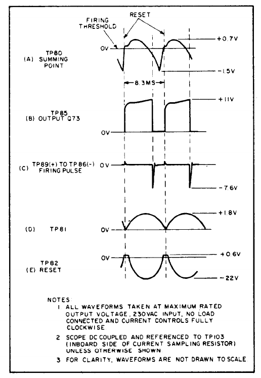
TM 11-6625-2958-14&P
ing current to the summing point, ensuring that the
triac will fire at low output “voltages.
4-24 The summation of the input signals results
in the generation of a voltage waveform at TP80
similar to that shown in waveform (A) of Figure 4-4.
When the linear ramp portion of the waveform
reaches a certain negative threshold voltage, di-
odes CR74 and CR75 become forward biased. The
negative voltage is then coupled to the base of
transistor Q72. Transistors Q72 and Q73 form a
squaring circuit resembling a Schmitt trigger con-
figuration. Q72 is conducting prior to firing time
due to the positive bias connected to its base
through R84, Transistor Q73 is cut off at this time
because its base is driven negative by the collect-
or of Q72.
4-25 When the negative threshold voltage is
reached, transistor Q72 is turned off and Q73 is
turned on. The conduction of Q73 allows capacitor
C71 to discharge rapidly through pulse transformer
T70 resulting in the generation of a firing pulse
across the secondary winding of T70. As shown in
Figure 4-4. Preregulator Control Circuit Waveforms
waveform (C) of Figure 4-4, the firing pulse is
quite narrow because Q73 saturates rapidly, causing
the magnetic field surrounding T70 to collapse. Di-
ode CR76 damps out positive overshoot.
4-26 Reset of the control circuit occurs once every
8.33 milliseconds when the rectified ac voltage at
the junction of CR77, CR78, and CR79 (TP82) in-
creases to a level at which diode CR78 becomes
forward biased. Summing capacitor C70 is then al-
lowed to discharge through CR78. Diodes CR74 and
CR75 become reverse biased at reset and transistor
Q72 reverts to its “on” state. Consequently, Q73
is turned off and capacitor C71 charges up through
R79 at a comparatively slow rate until the collector
voltage of Q73 reaches approximately +11 volts.
The above action causes the small positive spike
that appears across the windings of pulse transform-
er at T70 at reset time.
4-27 SERIES REGULATOR AND DRIVER
4-28 The series regulator consists of transistors
A4Q103 through A4Q108 connected in parallel. The
transistors serve as the series or “pass” element
which provides precise and rapid control of the out-
put. Resistors A4R150 through A4R155 allow high
output currents to be equally shared by the series
regulator transistors. The conduction of the series
transistors is controlled by signals obtained from
driver A4Q102, which is connected in a Darlington
configuration with the parallel-connected series
regulator transistors. Thermal switch A4TS101 opens
if the heat sink assembly temperature exceeds ap-
proximately 230°F, thus turning off the series regu-
lator transistors. This feature protects critical
components of the supply from excessive tempera-
tures which could occur if cooling fan A4B1 failed.
Diode CR50 provides a discharge path for the out-
put capacitors when the supply is rapidly down-
programmed; R57 limits the discharge current flow-
ing through the diode and through error amplifier
A4Q101. Diode A4CR105, connected across the reg-
ulator circuit, protects the series elements from
reverse voltages that could develop across them
during parallel operation if one supply is turned on
before the other.
4-29 SHORT CIRCUIT PROTECTION
4-30 This circuit acts to initially protect the series
regulator against a simultaneous full-voltage, full-
current conditions such as might occur if the output
were shorted when the controls were set to deliver
a high output voltage and current. Under this con-
dition, Q20 goes into heavy conduction due to the
increased voltage across the series regulator,
putting R26 in parallel with the current controls and
thus limiting the current to less than 10% of the
supply’s rating. Within 10 milliseconds after the
short circuit is imposed, the preregulator shuts off.
4-4
The input capacitor then begins to discharge through
the series regulator, and the voltage across the
regulator decreases until Q20 turns off. The dis-
charge time (typically ½ to 4 seconds) depends on
the voltage and current ratings of the supply, the
main filter capacitor, and the control settings.
Once this recovery time has elapsed, the output
current will return to the level set by the current
controls, and the preregulator will return the volt-
age across the series regulator to the normal 3.5V
level, thus limiting the power dissipated by the
s cries regulator.
4-31 CONSTANT VOLTAGE COMPARATOR
4-32 This circuit consists of the programming re-
sistors (A5R121 and A5R122) and a differential am-
plifier stage (Z1 and associated components). An
integrated circuit is used for the differential ampli-
fier to minimize differential voltages due to mis-
matched transistors and thermal differentials.
4-33 The constant voltage comparator continuously
compares the voltage drop across the VOLTAGE con-
trols with the output voltage and, if a difference
exists, produces an error voltage whose amplitude
is proportional to this difference. The error signal
ultimately alters the conduction of the series regu-
lator which, in turn, alters the output current so
that the output voltage becomes equal to the voltage
drop across the VOLTAGE controls. Hence, through
feedback action, the difference between the two in-
puts to Z1 is held at zero volts.
4-34 One input of the differential amplifier (pin
10) is connected to the output voltage sensing ter-
minal of the supply (+S) through impedance equaliz-
ing resistor R23. Resistors R1 and optional resistor
R110 are used to zero bias the input. If the supply
is equipped with Option 020, resistor R114 and po-
tentiometer R 113 provide a variable input bias that
allows the output voltage to be adjusted to exactly
zero volts when the supply is programmed for zero
output. The other input of the differential amplifier
(pin 1) is connected to a summing point (terminal
A2) at the junction of the programming resistors and
the current pullout resistors R3, R4, end R5. In-
stantaneous changes in the output voltage or
changes in the voltage at the summing point due to
manipulation of the VOLTAGE controls produce a dif-
ference voltage between the two inputs of the dif-
ferential amplifier. This difference voltage is am-
plified and appears at the output of the differential
amplifier (pin 12) as an error voltage which ulti-
mately varies the conduction of the series regulator.
4-3 S Resistor R6, in series with the summing-point
input to the differential amplifier, limits the cur-
rent through the programming resistors during rapid
voltage turn-down. Diode CR7 prevents excessive
current drain from the +6.2 volt reference supply
TM 11-6625-2958-14&P
during rapid down-programming; diodes CR5 and
CR6 prevent excessive voltage excursions from
over-driving the differential amplifier. Capacitor
C2 prevents the gain of the feedback loop from
changing during manipulation of the VOLTAGE con-
trols. Resistor R2 limits the discharge current
through C2. Resistors Z2F, Z2M, and Z2N bias the
differential amplifier; diode CR4 provides tempera-
ture compensation.
4-36 During constant voltage operation, the pro-
gramming current flowing through the programming
resistors (VOLTAGE controls) is held constant be-
cause the value of shunt resistor R3 is factory
selected to allow all of the +6.2 volt reference to
be dropped across R3, R4, and RS. Linear constant
voltage programming is thus assured with a constant
current flowing through A5R121 and A5R122. If the
supply is equipped with Option 020, resistor R111
and potentiometer R 112 allow the programming cur-
rent to be adjusted by varying the bias applied to
the summing point.
4-37 Main output capacitor A3C3 stabilizes the
series regulator feedback loop and helps supply
high-current pulses of short duration during con-
stant voltage pulse loading operation. An additional
output capacitor (C 19), connected directly across
the output bus bars, helps maintain a low ac output
impedance by compensating for the inductive react-
ance of the main output capacitor at high frequencies.
C19 also prevents any spikes in the output from
reaching the load.
4-38 CONSTANT CURRENT COMPARATOR
4-39 This circuit is similar in appearance and op-
eration to the constant voltage comparator circuit.
It consists of the coarse and fine current controls
(A5R123 and A5R124) and a differential amplifier
stage (Z 1 and associated components). As in the
constant voltage comparator, an integrated circuit
is used for the differential amplifier to minimize
differential voltages due to mismatched transistors
and thermal differentials.
4-40 The constant current comparator circuit con-
tinuously compares the voltage drop across the
CURRENT controls with the voltage drop across the
current sampling resistor, A4R123. If a difference
exists, the differential amplifier produces an error
signal which is proportional to this difference.
The remaining components in the feedback loop
(mixer amplifier, error amplifiers, and the series
regulator) function to maintain the voltage drop
across the current sampling resistors, and hence
the output current, at a constant value.
4-41 One input of the differential amplifier (pin 7)
is connected to the output bus through impedance
equalizing resistor R20 and is zero-biased by R21
4-5
TM 11-6625-2958-14&P
and optional resistor R 117. The other input of the
differential amplifier (pin 4) is connected to a sum-
ming point (terminal A6) at the junction of the pro-
gramming resistors and the current pullout resistors
R30 and R31. Changes in the output current due to
load changes or changes in the voltage at the sum-
ming point due to manipulation of the CURRENT
controls produce a difference voltage between the
two inputs of the differential amplifier. This differ-
ence voltage is amplified and appears at the output
of the differential amplifier (pin 6) as an error volt-
age which ultimately varies the conduction of the
s cries regulator.
4-42 Resistor R30 serves as a trimming adjustment
for the programming current flowing through A5R123
and A5R124. If the supply is equipped with Option
021, resistor R115 and potentiometer R116 provide
a means of adjusting the programming current. As
in the constant voltage comparator circuit, a vari-
able input bias (from resistor R118 and potentiome-
ter R119) is provided to allow the output current to
be adjusted to exactly zero when the supply is pro-
grammed for zero output. Diode CR21 limits exces-
sive voltage excursions at the summing-point input
to the differential amplifier.
4-43 VOLTAGE CLAMP CIRCUIT
4-44 The voltage clamp circuit keeps the constant
voltage programming current relatively constant
when the power supply is operating in the constant
current mode. This is accomplished by clamping
terminal A2, the voltage summing point, to a fixed
bias voltage. During constant current operation the
constant voltage programming resistors are a shunt
load acress the out put terminals of the power sup-
ply. When the output voltage changes, the current
through these resistors also tends to change. Since
this programming current flows through the current
sampling resistor, it is erroneously interpreted as
a load change by the current comparator circuit.
The clamp circuit eliminates this undesirable effect
by maintaining this programming current at a con-
stant level.
4-45 The voltage divider, Z2A, Z2B, and VR1, back
biases CR2 and Q1 during constant voltage opera-
t ion. When the power supply goes into constant
current operation, CR2 becomes forward biased by
the voltage at pin 12 of Z 1. This results in conduc-
tion of Q1 and the clamping of the summing point at
a potential only slightly more negative than the
normal constant voltage potential. Clamping this
voltage at approximately the same potential that
exists in constant voltage operation results in a
constant voltage acress, and consequently a con-
stant current through, the current pullout resistors
R3, R4, and R5.
4-46 MIXER AND ERROR AMPLIFIERS
4-47 The mixer and error amplifiers amplify the
error signal from the constant voltage or constant
current input circuit to a level sufficient to drive
the series regulating transistors. Mixer amplifier
Q41 receives the error voltage input from either the
constant voltage or constant current comparator via
the OR-gate diode (CR1 or CR20) that is conducting
at the time. Diode CR1 is forward biased and CR20
reverse biased during constant voltage operation.
The reverse is true during constant current opera-
tion.
4-48 Transistor Q40 provides a constant current to
the collector of Q41 and also generates a negative
going turn-off signal for the series regulator when
the unit is first turned off. Feedback network C41,
R47, and R53 shapes the high frequency rolloff in
the loop gain response in order to stabilize the
series regulator feedback loop.
4-49 Error amplifiers Q42 and A4Q101 serve as the
predriver elements for the series regulator. In addi-
tion, transistor A4Q101 allows faster down-program-
ming by providing a discharge path for output ca-
pacitors A3C3 and C19, and by supplying a bleed
current for the series regulator (thus keeping it in
its linear, active region) when the supply is set for
zero output current. Diode CR44, in the base cir-
cuit of transistor A4Q101, prevents the base from
going more negative than -3 volts. This action li-
mits the current through R57 to a relatively low
level, thus protecting A4Q101 from damage in the
event a voltage higher than the programmed output
voltage is placed across the output terminals (such
as might occur in Auto-Parallel or battery charging
applications).
4-50 OVERVOLTAGE PROTECTION CROWBAR
4-51 The overvoltage protection circuit protects
delicate loads from high voltage conditions such
as might result from the failure of the series regu-
lator transistor. It accomplishes this by shorting
the output of the supply. Under normal operation
(no overvoltage), Q92 is conducting since CR91 is
reverse biased and Q91 is off. Thus no trigger
signal is received by SCR A4CR110 and it acts as
an open circuit, having no effect on normal output
voltage.
4-52 A5R125 (OVERVOLTAGE ADJUST) adjusts the
bias of Q92 with relation to -S. It establishes the
point at which CR91 becomes forward biased and
Q92 is turned off. Zener diode VR90 provides a
stable reference voltage with which the -S potential
is compared; R95 sets the upper crowbar trip limit.
When Q92 turns off, Q91 begins to conduct, send-
ing a positive going trigger pulse to A4CR110,
causing it to create a near short circuit across the
4-6
output. When A4CR110 is fired, overvoltage lamp
A5DS2 is tuned on, completing a path for a + 11V
unregulated holding current through A5DS2. This
current holds A4CR110 on even after the output
voltage has fallen. A4 CR110 will remain in conduc-
tion until the supply is turned off. R92 supplies the
holding current if lamp A5DS2 should open. R106
protects A4CR108 and A4CR110 from the large surge
current that occurs when A4CR110 is first fired.
CR93 damps out positive overshoot in the trigger
pulse.
4-53 The firing of SCR A4CR110 biases Q90 into
conduction, placing approximately +11 volts on the
cathode of CR74 in the preregulator control circuit
and thus reverse biasing CR74 and CR75. This
action, by preventing transistor Q 72 from turning
off, prevents the generation of any trigger pulses
and turns off the preregulator. This prevents the
series regulator from experiencing a full-voltage,
full-current condition.
4-54 The crowbar circuit creates an extra current
path during normal operation of the supply, thus
changing the current that flows through the sam-
pling resistor. Diode CR92 keeps this extra current
at a fixed level for which compensation can then be
made in the constant current comparator circuit.
4-55 A slaving arrangement of crowbar circuits in
more than one unit is made possible by an extra
secondary winding (terminals 5 and 6) on transfor-
mer T90. Terminals on the rear barrier strip (±EXT.
CROWBAR TRIGGER) allow easy connection to this
winding. Connecting these windings in parallel
when operating in a multiple-supply configuration
will result in all the crowbars being activated if
one of the crowbars is tripped. To reset the crow-
bars in this arrangement, all of the units must be
turned off and then on. Correct polarity must be
observed when connecting the windings in parallel.
Figures 3-10 and 3-11 (Auto-Parallel and Auto-
Series ) demonstrate these connections.
4-56 TURN-ON CONTROL CIRCUIT
4-57 This circuit is a long time-constant network
which protects the triac and the series regulator
from possible damage during turn-on. When the
supply is first tuned on, C35 provides a positive
voltage to the anodes of CR35 and CR36. The volt-
age from CR35 is connected to the cathode of diode
CR74 in the preregulator control circuit to ensure
that it is initially reverse biased. After C35 be-
comes sufficiently charged, diode CR35 becomes
reverse biased and the preregulator control circuit
is permitted to fire the triac.
4-58 Diode CR36 performs a similar function for
the series regulator. CR36 initially couples a pos-
itive voltage to Q41 where it is inverted and ap-
TM 11-6625-2958-14&P
plied to the series regulator. This negative voltage
keeps the regulator cut off untill C35 charges up.
Diode CR37 provides a discharge path for C35 when
the supply is turned off.
4-59 REFERENCE REGULATOR
4-60 The reference circuit is a feedback power
supply similar to the main supply. It provides
stable reference voltages used throughout the unit.
AH the reference voltages are derived from dc ob-
tained from full wave rectifier CR61-CR62 and filter
capacitor C61. The total output of the reference
circuit is 18.6V. Zener diodes VR60 and VR61 es-
tablish moderately well regulated potentials of
+6.2V and -6.2V respectively from the common point
+S, while the regulator circuit establishes a very
well regulated potential of +12.4 volts from +S.
Resistor R63 limits the current through the Zener
diodes to establish an optimum bias level.
4-61 The regulating circuit consists of s cries reg-
ulating transistor Q60, driver Q61, and differential
amplifier Q62 and Q63. The voltage across Zener
diode VR60 (+6.2 volts with respect to +S) and the
voltage at the junction of divider Z2L-R69B and Z2J
are compared, and any difference is amplified by
Q 62 and Q63. The error voltage thus appearing at
the collector of Q62 is amplified by driver stage
Q61 and applied to series regulator Q60 in the cor-
rect phase and amplitude to maintain the +12.4 volt
output at a constant level.
4-62 Diode CR60, connected from voltage divider
R66 and R67 to the base of Q61, serves as a turn-
on circuit for series regulator transistor Q60. When
the supply is first turned on, CR60 biases driver
Q61 on, thus turning on the series regulator. When
the reference supply reaches normal output, the
base voltage of Q61 is sufficient to reverse bias
CR60, thus effectively removing it from the circuit.
Capacitor C60, connected across the output of the
reference supply, removes spikes and stabilizes
the reference reguIator loop.
4-63 Unregulated 11Vdc is supplied from a sepa-
rate winding on transformer A3T2 by diodes CR53
and CR54 and filter capacitor C44. Additional light-
ly regulated reference voltages of -4V and -2.4V are
provided by diodes CR45-CR46 and CR47-CR48-CR49
respectively. Diode CR43 prevents reverse current
flow from damaging the main supply series reguIator
transistors. Diode CR7, shown in the schematic
near the current pullout resistors (R3, R4, and RS),
protects the Zener diodes in the reference circuit
by providing a path for surge currents which occur
during rapid down programming.
4-64 METER CIRCUIT
4-65 The meter circuit provides continuous indica-
4-7
TM 11-6625-2958-14&P
tions of output voltage and current on the dc volt-
meter and ammeter. Both meter movements can
withstand an overload of many times the maximum
rated output without damage.
4-66 The ammeter together with its series resistors
(R101, R105) is connected across current sampling
resistor A4R123. As mentioned previously, the
voltage drop across the current sampling resistor
varies in proportion to the output current. Potenti-
ometer R101 is adjusted for full scale deflection
(calibration) of the ammeter.
4-67 The voltmeter, in series with R103 and R104
and shunted by R102 and R106, is connected direct-
ly across the output terminals of the supply. Poten-
tiometer R106 permits calibration of the voltmeter.
4-68 ADDITIONAL PROTECTION FEATURES
4-69 The supply contains several “special pur-
pose” components which protect the supply in the
event of unusual circumstances. One of these
components is diode A4CR106. Connected across
the output terminals of the supply, it prevents in-
ternal damage from reverse voltages that might be
applied across the supply. This could occur, for
example, during Auto-Series operation if one sup-
ply was turned on before the other.
4-70 Resistors R108 and R109 limit the output of
the supply if the connections between both output
buses and the sensing terminals (+S and -S) are in-
advertently removed.
4-71 Diode A4CR105, previously mentioned in the
series regulator description, protects the regula-
ting transistor from the effects of reverse voltages.
4-8
TM 11-6625-2958-14&P
SECTION V
MAINTENANCE
5-1 INTRODUCTION
5-2 Upon receipt of the power supply, the per-
formance check (Paragraph 5-5) should be made.
This check is suitable for incoming inspection. If
a fault is detected in the power supply while mak-
ing the performance check or during normal opera-
tion, proceed to the troubleshooting procedures
(Paragraph 5-51). After troubleshooting and repair
returning the power supply to normal operation, re-
peat the performance check to ensure that the fault
has been properly corrected and that no other faults
exist. Before performing any maintenance checks,
turn on the power supply and allow a half-hour
warm-up.
5-3 TEST EQUIPMENT REQUIRED
5-4 Table 5-1 lists the test equipment required to
(Paragraph 5-71), perform any necessary adjust- perform the various procedures described in this
ments and calibrations (Pare graph 5-73). Before section.
Table 5-1. Test Equipment Required
TYPE
REQUIRED
USE
RECOMMENDED
CHARACTERISTICS
MODEL
Differential
I
Sensitivity: 1mV full scale (min.)
Voltmeter Input impedance: 10M Ω (rein.)
Oscilloscope Sensitivity and bandwidth;
100µV/cm and 400KHz for all
measurements except noise spike;
5mV sensitivity and 20 MHz band-
width for noise spike measure-
ment.
Measure dc voltages;
calibration procedures.
Measure ripple; display
transient recovery wave-
form; measure noise
spikes.
3420A/B (See
Note on Page 5-2)
140A with 1423A
time base and
1400A vertical
plug-in; 1402A
plug-in for spike
measurement.
Variable
Voltage
Transformer
Range: 207-253Vac. Recommend-
ed minimum output current: 12A,
6259B; 22A, 6261B and 6268B;
24A, 6260B: 36A, 6269B.
Vary ac input for line
regulation measurement.
----
AC Voltmeter Sensitivity: 1mV full scale de- Measure ac voltages and
403B
flection (min). Accuracy: 2%. ripple.
DC Voltmeter
I
Sensitivity: 1mV full scale de- Measure dc voltages.
I
412A
flection (rein). Accuracy: 1%.
Repetitive
I
Switching rate: 60-400Hz
I
Measure transient re- See Figure 5-5.
Load Stitch Rise time: 2µsec. covery time.
Resistive
I
Values: see Figures 5-2 and 5-5. Power supply load ----
Loads
resistors.
Current
Sampling
Resistors
Values: see Figure 5-8. Measure output current;
calibrate ammeter.
A4R123;
:
A4R123A-
A4R123B,
6260B only; see
Replaceable Parts
IITable.
5-1
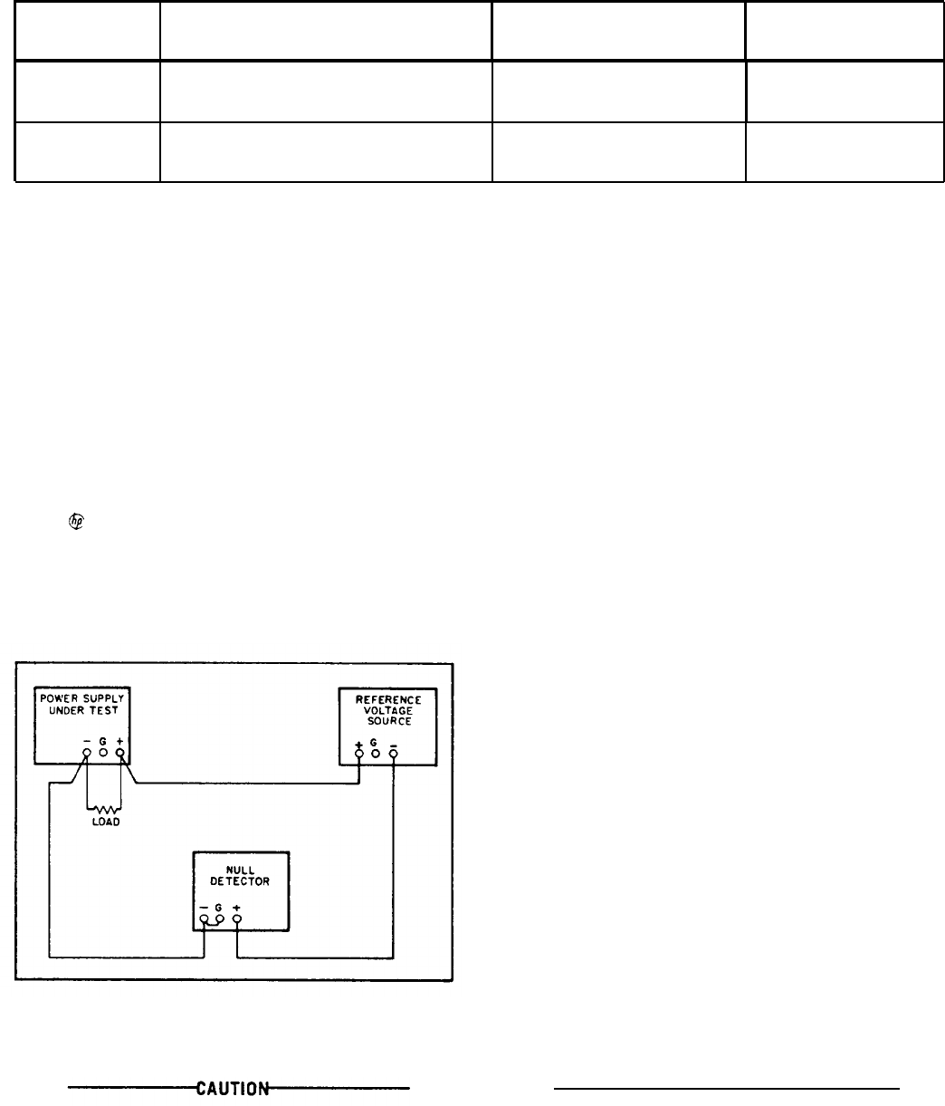
TM 11-6625-2958-14&P Table 5-1. Test Equipment Required (Continued)
TYPE
REQUIRED
RECOMMENDED
CHARACTERISTICS
USE
MODEL
Terminating Value: 50 ohms, ½ watt, ±5%, Noise spike measure- ----
Resistors non-inductive. (Four required.) ment.
Blocking Value: 0.01µF, 100Vdc. (Two Noise spike measure- ----
Capacitors required.) ment.
1
NOTE
A satisfactory substitute for a differen-
tial voltmeter is a reference voltage
source and null detector arranged as
shown in Figure 5-1. The reference
voltage source is adjusted so that the
voltage difference between the supply
being measured and the reference volt-
age will have the required resolution
for the measurement being made. The
voltage difference will be a function of
the null detector that is used. Exam-
ples of satisfactory null detectors are:
419A null detector, a dc coupled
oscilloscope utilizing differential in-
put, or a 50mV meter movement with a
100 division scale. For the latter, a
2mV change in voltage will result in a
meter deflection of four divisions.
Figure 5-1. Differential Voltmeter Substitute
Test Setup
Care must be exercised to avoid ground
loops and circulating currents when
using an electronic null detector in
which one input terminal is grounded.
5-5 PERFORMANCE TEST
5-6 The following test can be used as an incoming
inspection check and appropriate portions of the
test can be repeated either to check the operation
of the instrument after repairs or for periodic main-
tenance tests. The tests are performed using a 230V
ac, 60 Hz, single phase input power source. If the
correct result is not obtained for a particular check,
do not adjust any internal controls; proceed to
troubleshooting (Paragraph 5-5 1).
5-7 CONSTANT VOLTAGE TESTS
5-8 If maximum accuracy is to be obtained in the
following measurements, the measuring devices
must be connected as close to the output terminals
as possible. This is particularly important when
measuring the transient response, regulation, or
ripple of the power supply. A measurement made
across the load includes the impedance of the leads
to the load and such lead lengths can easily have
an impedance several orders of magnitude greater
than the supply impedance, thus invalidating the
measurement.
5-9 To avoid mutual coupling effects, each moni-
toring device must be’ connected to the output ter-
minals by a separate pair of leads. Twisted pairs
or shielded two-wire cables should be used to avoid
pickup on the measuring leads. The load resistor
should be connected across the output terminals as
close to the supply as possible. When measuring
the constant voltage performance specifications, the
current controls should be set well above (at least
10%) the maximum output current which the supply
will draw, since the onset of constant current
action will cause a drop in output voltage, increased
ripple, and other performance changes not properly
ascribed to the constant voltage operation of the
supply .
5-10 Voltage Output and Voltmeter Accuracy. To
check the output voltage, proceed as follows:
a. Connect load resistor (RL) indicated in
Figure 5-2 across output terminals of supply.
b. Connect differential voltmeter acress
+OUT and -OUT terminals of supply, observing
5-2
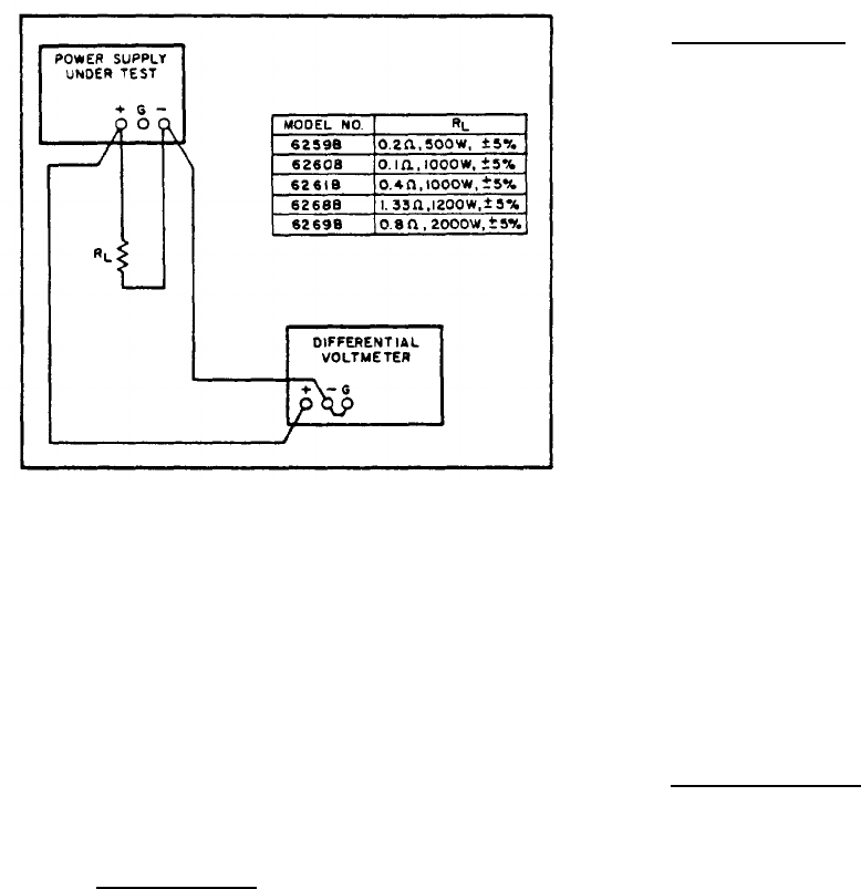
Figure 5-2. Constant Voltage Load Regulation
Test Setup
correct polarity.
c. Turn CURRENT controls fully clockwise.
d. Turn on supply and adjust VOLTAGE con-
trols until front panel meter indicates exactly max-
imum rated output voltage.
e. Differential voltmeter should indicate the
following:
5-11
5-12
tion,
6259B, 6260B
10 ±0.2Vdc
6261B
20 ±0.4Vdc
6268B, 6269B
40 ±0.8Vdc
Load Regulation.
Definition: The change ∆ EOUT in the
static value of dc output voltage re-
sulting from a change in load resist-
ance from open circuit to a value
which yields maximum rated output
current (or vice versa).
To check the constant voltage load regula-
proceed as follows:
‘a. Connect test setup shown in Figure 5-2.
b. Turn CURRENT controls fully clockwise.
c. Turn on supply and adjust VOLTAGE con-
trols until front panel meter indicates exactly max-
imum rated output current.
d. Read and record voltage indicated on dif-
ferential voltmeter.
e. Disconnect load resistor.
f. Reading on differential voltmeter should
not vary from reading recorded in Step (d) by more
than the following:
6259B, 6260B 1.2mV
6261B
2.2mV
6268B, 6269B 4.2mV
5-13
5-14
TM 11-6625-2958-14&P
Line Regulation.
Definition: The change ∆ EOUT in the
static value of dc output voltage re-
sulting from a change in ac input volt-
age over the specified range from low
line (usually 207 volts) to high line
(usually 253 volts), or from high
line to low line.
To check the line regulation, proceed as
follows :
a. Connect test setup shown in Figure 5-2.
b. Connect variable auto transformer between
input power source and power supply power input.
c. Adjust variable auto transformer for 207
volts a c input.
d. Turn CURRENT controls fully clockwise.
e. Turn on supply and adjust VOLTAGE con-
trols until front panel meter indicates exactly maxi-
mum rated output voltage.
f. Read and record voltage indicated on dif-
ferential voltmeter.
g. Adjust variable auto transformer for 253V
ac input.
h. Reading on differential voltmeter should
not vary from reading recorded in Step (f) by more
than the following:
5-15
6259B,6260B
1.2mV
6261B
2.2mV
6268B, 6269B 4.2mV
Ripple and Noise.
Definition: The residual ac voltage
superimposed on the dc output of a
regulated power supply. Ripple and
noise may be specified and measured
in terms of its RIMS or (preferably)
peak-to-peak value.
Ripple and noise measurement can be made at any
input ac line voltage combined with any dc output
voltage and load current within the supply's rating.
5-16 The amount of ripple and noise that is pres-
ent in the power supply output is measured either
in terms of the RMS or (preferably) peak-to-peak
value. The peak-to-peak measurement is particu-
larly important for applications where noise spikes
could be detrimental to a sensitive load, such as
logic circuitry. The RMS measurement is not an
ideal representation of the noise, since fairly high
output noise spikes of short duration can be pres-
ent in the ripple without appreciably increasing the
RMS value,
5-17 Ripple Measurements. Figure 5-3A shows an
incorrect method of measuring p-p ripple. Note
that a continuous ground loop exists from the third
wire of the input power cord of the supply to the
third wire of the input power cord of the oscillo-
scope via the grounded power supply case, the
5-3
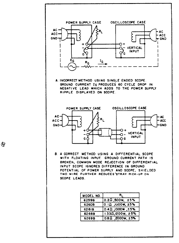
TM 11-6625-2958-14&P
wire between the negative output terminal of the
power supply and the vertical input of the scope,
and the grounded scope case. Any ground current
circulating in this loop as a result of the difference
in potential EG between the two ground points
causes an IR drop which is in series with the scope
input. This IR drop, normally having a 60Hz line
frequency fundamental, plus any pickup on the un-
shielded leads interconnecting the power supply
and scope, appears on the face of the CRT. The
magnitude of this resulting noise signal can easily
be much greater than the true ripple developed be-
tween the plus and minus output terminals of the
power supply, and can completely invalidate the
measurement.
5-18 The same ground current and pickup problems
can exist if an RMS voltmeter is substituted in
place of the oscilloscope in Figure 5-3. However,
the oscilloscope display, unlike the true RMS
meter reading, tells the observer immediately
whether the fundamental period of the signal dis-
played is 8.3 milliseconds (1/120 Hz) or 16.7 milli-
seconds (1/60 Hz). Since the fundamental ripple
frequency present on the output of an
120Hz (due to full-wave rectification), an oscillo-
scope display showing a 120Hz fundamental com-
ponent is indicative of a “clean” measurement set-
up, while the presence of a 60Hz fundamental
usually means that an improved setup will result in
a more accurate (and lower) value of measured rip-
ple.
5-19 Although the method shown in Figure 5-3A is
not recommended for ripple measurements, it may
prove satisfactory in some instances provided cer-
tain precautionary measures are taken. One meth-
od of minimizing the effects of ground current (IG)
flow is to ensure that both the supply and the test
instrument are plugged into the same ac power
buss.
5-20 To minimize pick up, a twisted pair or (pref-
erably) a shielded two-wire cable should be used
to connect the output terminals of the power supply
to the vertical input terminals of the scope. When
using a twisted pair, care must be taken that one
of the two wires is connected both to the grounded
terminal of the power supply and the grounded input
terminal of the oscilloscope. When using shielded
two-wire cable, it is essential for the shield to be
connected to ground at one end only to prevent any
ground current flowing through this shield from in-
ducing a signal in the shielded leads.
5-21 To verify that the oscilloscope is not dis-
playing ripple that is induced in the leads or pick-
ed up from the grounds, the (+) scope lead should
be shorted to the (-) scope lead at the power sup-
ply terminals. The ripple value obtained when the
leads are shorted should be subtracted from the
Figure 5-3. Ripple Test Setup
actual ripple measurement.
5-22 If the foregoing measures are used, the
single-ended scope of Figure 5-3A may be adequate
to eliminate non-real components of ripple so that
a satisfactory measurement can be obtained. How-
ever, in stubborn cases or in measurement situa-
tions where it is essential that both the power sup-
ply case and the oscilloscope case be connected
to ground (e. g. if both are rack-mounted), it may
be necessary to use a differential scope with
floating input as shown in Figure 5-3B. If desired,
two single-conductor shielded cables may be sub-
stituted in place of the shielded two-wire cable
with equal success.
5-4
supply is
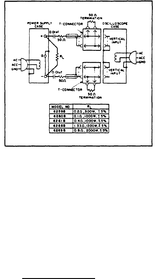
Because of its common mode rejection, a differen-
tial oscilloscope displays only the difference in
signal between its two vertical input terminals,
thus ignoring the effects of any common mode sig-
nal produced by the difference in the ac potential
between the power supply case and scope case.
Before using a differential input scope in this man-
ner, however, it is imperative that the common
mode rejection capability of the scope be verified
by shorting together its two input leads at the pow-
er supply and observing the trace on the CRT. If
this trace is a straight line, then the scope is pro-
perly ignoring any common mode signal present. If
this trace is not a straight line, then the scope is
not rejecting the ground signal and must be realign-
ed in accordance with the manufacturer’s instruc-
tions until proper common mode rejection is attain-
ed.
5-23 To check the ripple output, proceed as fol-
lows :
a. Connect oscilloscope or RMS voltmeter
as shown in Figures 5-3A or 5-3B.
b. Turn CURRENT controls fully clockwise.
c. Adjust VOLTAGE controls until front panel
meter indicates maximum rated output voltage.
d. The observed ripple should be less than
the following:
6259B, 6260B, 6261B
500µVrms and 5mV p-p
6268B, 6269B
1mVrms and 5mV p-p
5-24 Noise Spike Measurement. When a high fre-
quency spike measurement is being made, an in-
strument of sufficient bandwidth must be used; an
oscilloscope with a bandwidth of 20 MHz or more is
adequate. Measuring noise with an instrument that
has insufficient bandwidth may conceal high fre-
quency spikes detrimental to the load.
5-25 The test setup illustrated in Figure 5-3A
is generally not acceptable for measuring spikes;
a differential oscilloscope is necessary. Further-
more, the measurement concept of Figure 5-3B
must be modified if accurate spike measurement
is to be achieved
1. As shown in Figure 5-4, twO coax cables
must be substituted for the shielded two-wire cable.
2. Impedance matching resistors must be in-
cluded to eliminate standing waves and cable ring-
ing, and capacitors must be inserted to block the
dc current path.
3. The length of the test leads outside the
coax is critical and must be kept as short as pos-
sible; the blocking capacitor and the impedance
matching resistor should be connected directly from
the inner conductor of the cable to the power supply
terminals.
4. Notice that the shields of the power sup-
ply end of the two coax cables are not connected to
the power supply ground, since such a connection
would give rise to a ground current path through the
TM 11-6625-2958-14&P
Figure 5-4. Noise Spike Measurement Test Setup
coax shield, resulting in an erroneous measurement.
5. Since the impedance matching resistors
constitute a 2-to-1 attenuator, the noise spikes
observed on the oscilloscope should be less than
2.5mV p-p instead of 5mV p-p.
5-26 The circuit of Figure 5-4 can also be used for
the normal measurement of low frequency ripple:
simply remove the four terminating resistors and
the blocking capacitors and substitute a higher gain
vertical plug-in in place of the wide-band plug-in
required for spike measurements. Notice that with
these changes, Figure 5-4 becomes a two-cable
version of Figure 5-3B.
5-27 Transient Recovery Time.
Definition: The time "X" for the output
voltage recovery to within "Y" millivolts
of the nominal output voltage following a
"Z" amp step change in load current,
where: "Y" is specified as 10mV, the
nominal output Voltage is defined as the
dc level ‘halfway between the static out-
put voltage before and after the imposed
load change, and "Z" is the specified
load current change of S amps or the full
load current rating of the supply, which-
ever is less.
5-28 Transient recovery time may be measured at
any input line voltage combined with any output
voltage and load current within rating,
5-29 Reasonable care must be taken in switching
the load resistance on and off. A ha rid-operated
s-s
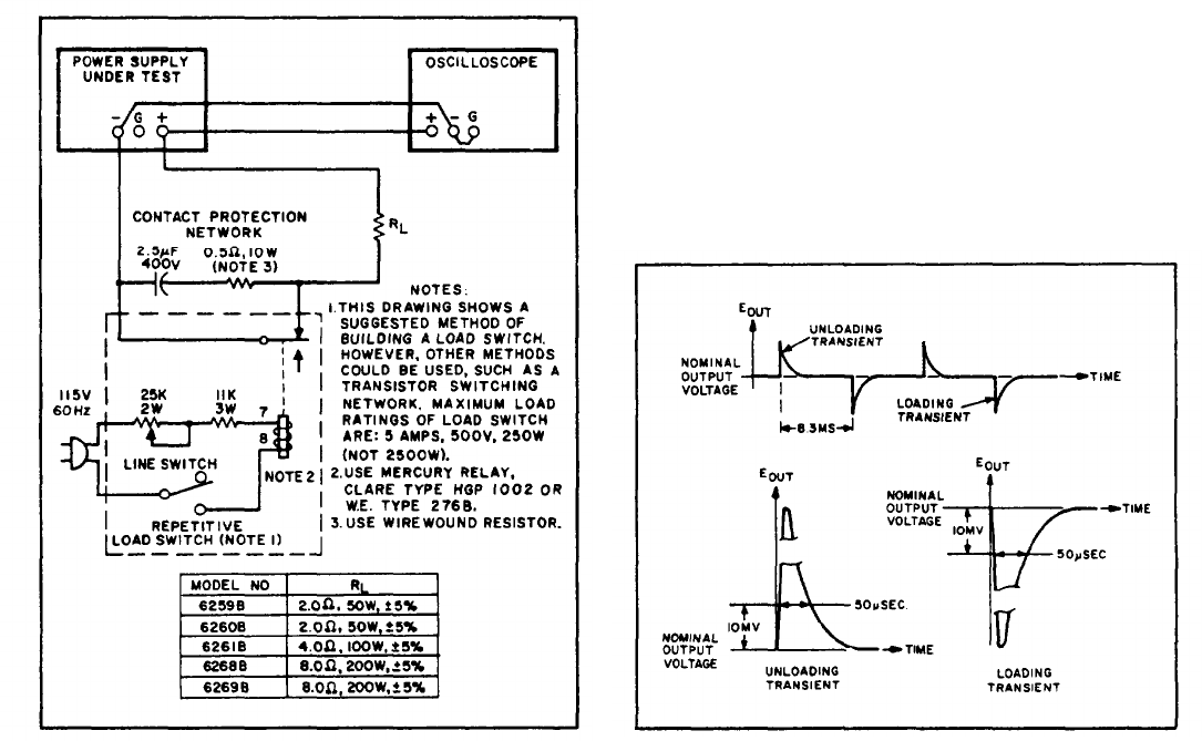
TM 11-6625-2958-14&P
switch in series with the load is not adequate,
since the resulting one-shot displays are difficult
to observe on most oscilloscopes, and the arc
energy occurring during switching action completely
masks the display with a noise burst. Transistor
load switching devices are expensive if reasonably
rapid load current changes are to be achieved.
5-30 A mercury-wetted relay, as connected in the
load switching circuit of Figure 5-5 should be used
for loading and unloading the supply. When this
load switch is connected to a 60Hz ac input, the
mercury-wetted relay will open and close 60 times
per second. Adjustment of the 25K control permits
adjustment of the duty cycle of the load current
switching and reduction in jitter of the oscilloscope
display.
5-31 The load resistances shown in Figure 5-5 are
the minimum resistances that must be used in order
to preserve the mercury-wetted relay contacts.
Switching of larger load currents can be accom-
plished with mercury pool relays; with this tech-
nique fast rise times can still be obtained, but the
large inertia of mercury pool relays limits the max-
imum repetition rate of load switching and makes
the clear display of the transient recovery charac-
teristic on oscilloscope more difficult.
5-32 To check the transient recovery time, pro-
ceed as follows:
a. Connect test setup shown in Figure 5-5.
b. Turn CURRENT controls fully clockwise.
c. Turn on supply and adjust VOLTAGE con-
trols until front panel ammeter indicates 5 amps
output current.
d. Close line switch on repetitive load
switch setup.
e. Set oscilloscope for internal sync and
lock on either positive or negative load transient
spike.f. Set vertical input of oscilloscope for ac
coupling so that small dc level changes in power
supply output voltage will not cause display to
shift. g. Adjust the vertical centering on the scope
so that the tail ends of the no load and full load
waveforms are symmetrically displayed about the
horizontal center line of the oscilloscope. This
center line now represents the nominal output volt-
age defined in the specification.
h. Adjust the horizontal positioning control
so that the trace starts at a point coincident with a
major graticule division. This point is then repre-
sentative of time zero.
i.Increase the sweep rate so that a single
transient spike can be examined in detail.
j. Adjust the. sync controls separately for
the positive and negative going transients so that
not only the recovery waveshape but also as much
as possible of the rise time of the transient is dis-
played.
k. Starting from the major graticule division
representative of time zero, count to the right 50µ-
sec and vertically 10mV. Recovery should be with-
in these tolerances as illustrated in Figure 5-6.
Figure 5-5. Transient Recovery Time Test Setup
5-6
Figure 5-6. Transient Recovery Time Waveforms

5-33 Temperature Coefficient.
Definition: The change in output volt-
age per degree Centigrade change in
the ambient temperature under condi-
tions of constant input ac line voltage,
output voltage setting, and load re-
sistance.
5-34 The temperature coefficient of a power supply
is measured by placing the power supply in an oven
and varying it over any temperature span within its
rating. (Most HP power supplies are rated for oper-
ation from 0°C to 55°C.) The power supply must be
allowed to thermally stabilize for a sufficient period
of time at each measurement temperature.
5-35 The temperature coefficient given in the spec-
ifications is the maximum temperature-dependent
output voltage change which will result over any one
degree Centigrade interval. The differential volt-
meter or digital voltmeter used to measure the out-
put voltage change of the supply should be placed
outside the oven and should have a long term sta-
bility adequate to insure that its drift will not affect
the overall measurement accuracy.
5-36 To check the temperature coefficient, pro-
ceed as follows:
a. Connect load resistance and differential
voltmeter as illustrated in Figure 5-2.
b. Turn CURRENT controls fully clockwise.
c. Adjust front panel VOLTAGE controls until
front panel voltmeter indicates maximum rated out-
put voltage.
d. Place power supply in temperature-con-
trolled oven (differential voltmeter remains outside
oven). Set temperature to 30°C and allow 30 minutes
warm-up.
e. Record differential voltmeter reading.
f. Raise temperature to 40°C and allow 30
minutes warm-up.
g. Observe differential voltmeter reading.
Difference in voltage reading between Step (e) and
(g) should be less than the following:
62599,62600
12mV
6261B
22mV
6268B, 6269B
42mV
5-37 Qutput Stability.
Definition: The change in output voltage
for the first eight hours following a 30-
minute warm-up period. During the in-
terval of measurement all parameters,
such as load resistance, ambient temp-
erature, and input line voltage are held
constant.
5-38 This measurement is made by monitoring the
output of the power supply on a differential voltme-
ter or digital voltmeter over the stated measurement
interval; a strip chart recorder can be used to
TM 11-6625-2958-14&P
provide a permanent record. A thermometer should
be placed near the supply to verify that the ambi-
ent temperature remains constant during the period
of measurement. The supply should be put in a lo-
cation immune from stray air currents (open doors
or windows, air conditioning vents); if possible,
the supply should be placed in an oven which is
held at a constant temperature. Care must be taken
that the measuring instrument has a stability over
the eight hour interval which is at least an order of
magnitude better than the stability specification of
the power supply being measured. Typically, a
supply may drift Iess over the eight hour measure-
ment interval than during the half-hour warm-up.
5-39 To check the output stability, proceed as
follows :
a. Connect load resistance and differential
voltmeter as illustrated in Figure 5-2.
b. Turn CURRENT controls fully clockwise.
c. Adjust front panel VOLTAGE controls until
differential voltmeter indicates maximum rated out-
put voltage.
d. Allow 30 minutes warm-up, then record
differential voltmeter reading.
e, After 8 hours, differential voltmeter should
change from reading recorded in Step (d) by less
then the following:
6259B, 62600
5.0mV
6261B, 6268B 8.0mV
6269B 14.0mV
5-40 CONSTANT CURRENT TESTS
5-41 The instruments, methods, and precautions
for the proper measurement of constant current pow-
er supply characteristics are for the most part iden-
tical to those already described for the measurement
of constant voltage power supplies. There are,
however, two main differences: first, the power
supply performance will be checked between short
circuit and full load rather than open circuit and full
load. Second, a current monitoring resistor is in-
serted between the output of the power supply and
the load.
5-42 For all output current measurements the cur-
rent sampling resistor must be treated as a four
terminal device. In the manner of a meter shunt,
the load current is fed to the extremes of the wire
leading to the resistor while the sampling terminals
are located as close as possible to the resistance
portion itself (see Figure 5-7). Generally, any cur-
rent sampling resistor should be of the low noise,
low temperature coefficient (Iess then 30ppm/°C)
type and should be used at no more than 5% of its
rated power so that its temperature rise will be
minimized, If difficulty is experienced in obtaining
a low resistance, high current resistor suitable for
current sampling, a duplicate of the sampling resis-
tor used in this unit (A4R123 or A4R123A-A4R123B)
5-7
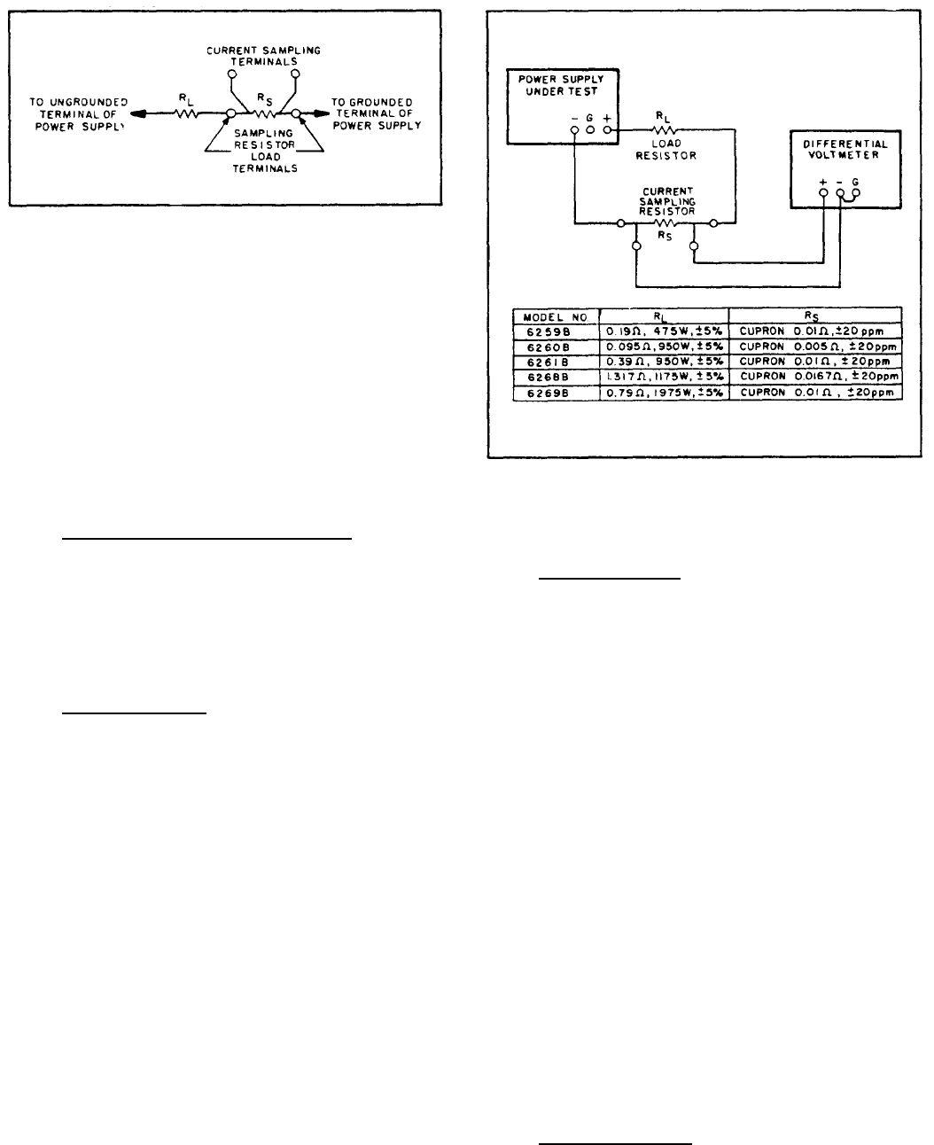
TM 11-6625-2958-14&P
Figure 5-7. Current Sampling Resistor Connections
NOTE
When using the HP current sampling
resistor recommended for this instru-
ment, an external fan must be employed
to cool the resistor. This precaution
will maintain the sampling resistance
at a constant value.
may be obtained from the factory.
5-43 Rated Output and Meter Accuracy.
a. Connect test setup shown in Figure 5-8.
b. Turn VOLTAGE controls fully clockwise.
c. Turn on supply and adjust CURRENT con-
trols until front panel ammeter indicates maximum
rated output current.
d. Differential voltmeter should read 0.5 ±
0.01Vdc.
5-44
5-45
Load Regulation.
Definition: The change ∆ IOUT in the
static value of the dc output current
resulting from a change in load re-
sistance from short circuit to a value
which yields maximum rated output
voltage.
To check the constant current load regulation,
proceed as follows:
a. Connect test setup shown in Figure 5-8.
b. Turn VOLTAGE controls fully clockwise.
c. Adjust CURRENT controls until front panel
meter reads exactly maximum rated out voltage.
d. Read and record voltage indicated on dif-
ferential voltmeter.
e, Short circuit load resistor (RL).
f. Reading on differential voltmeter should
not vary from reading recorded in Step (d) by more
than the following:
6259B 110µv
6260B 110µv
6261B 110µv
6268B 134µv
6269B
120µV
Figure 5-8. Constant Current Load Regulation
Test Setup
5-46 Line Regulation.
Definition: The change ∆ IOUT in the
static value of dc output current re-
sulting from a change in ac input volt-
age over the specified range from low
line (usually 207 volts) to high line
(usually 253 volts), or from high
line to low line.
5-47 To check the line regulation, proceed as fol-
lows: a. Utilize test setup shown in Figure 5-8.
b. Connect variable auto transformer between
input power source and power supply power input.
c. Adjust auto transformer for 207Vac input.
d. Turn VOLTAGE controls fully clockwise.
e. Adjust CURRENT controls until front panel
ammeter reads exactly maximum rated output current.
f. Read and record voltage indicated on dif-
ferential voltmeter.
g. Adjust variable auto transformer for 253V
ac input.
h. Reading on differential voltmeter should
not vary from reading recorded in Step (f) by more
than the following:
5-48
6259B, 6269B
120µV
6260B, 6261B
110µV
6268B
134µV
Ripple and Noise.
Definition: The residual ac current which
is superimposed on the dc output current
5-8
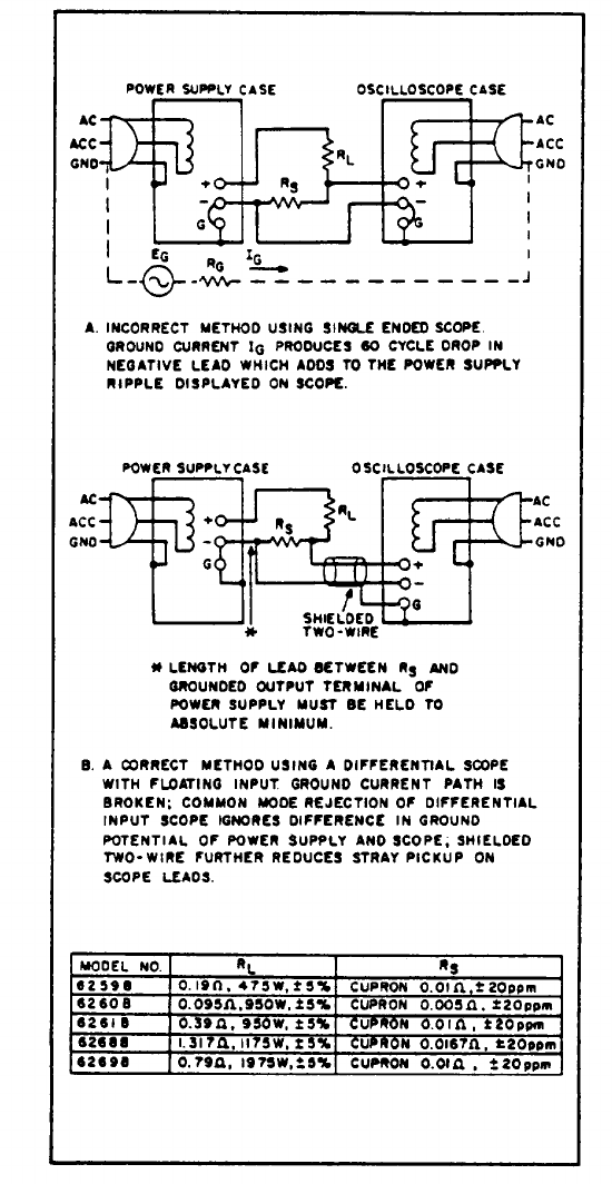
Figure 5-9. Constant Current Ripple and Noise
s -49
Test Setup
of a regulated power supply. AC ripple
and noise current is usually specified
and measured in terms of its RMS
value.
Most of the instructions pertaining to the
ground loop and pickup problem-s associated with
constant voltage ripple and noise measurement
TM 11-6625-2958-14&P
also apply to the measurement of constant current
ripple and noise. Figure 5-9 illustrates the most
important precautions to be observed when measur-
ing the ripple and noise of a constant current sup-
ply. The presence of a 120Hz waveform on the os-
cilloscope is normally indicative of a correct mea-
surement method. A waveshape having 60Hz as its
fundamental component is typically associated with
an incorrect measurement setup.
5-50 Ripple and Noise Measurement. To check
the ripple and noise, proceed as follows:
a. Connect oscilloscope or RMS voltmeter
as shown in Figures 5-9A or 5-9B.
b. Turn VOLTAGE controls fully clockwise.
c. Adjust CURRENT controls until front pan-
e 1 ammeter reads exactly maximum rated output cur-
rent. d. The observed ripple and noise should be
less than:
6259B
250µVrms
6260B
250µVrms
6261B
250µVrms
6268B
334µVrms
6269B
250µVrms
5-51 TROUBLESHOOTING
5-52 Before attempting to troubleshoot this instru-
ment, ensure that the fault is with the instrument
and not with an associated circuit. The perform-
ance test (Paragraph 5-5) enables this to be deter-
mined without having to remove the instrument from
the cabinet.
5-53 A good understanding of the principles of op-
eration is a helpful aid in troubleshooting, and it
is recommended that the reader review Section IV
of the manual before attempting to troubleshoot the
unit in detail. Once the principles of operation are
understood, refer to the overall troubleshooting
procedures in Paragraph S-S 6 to locate the symptom
and probable cause.
5-54 The schematic diagram at the rear of the
manual (Figure 7-11) contains normal voltage read-
ings taken at various points within the circuits.
These voltages are positioned adjacent to the ap-
plicable test points (identified by encircled num-
bers). The component location diagrams (Figures
7-1 through 7-8, and Figure 7-10) at the rear of the
manual should be consulted to determine the loca-
tion of components and test points.
5-55 If a defective component is located, replace
it and re-conduct the performance test. When a
component is replaced, refer to the repair and re-
placements (Paragraph 5-71) and adjustment and
calibration (Paragraph 5-73) sections of this man-
ual
5-9

TM 11-6625-2958-14&P
5-56 OVERALL TROUBLESHOOTING PROCEDURE
5-57 To locate the cause of trouble, follow Steps
1, 2, and 3 in sequence:
(1) Check for obvious troubles such as trip-
ped circuit breaker, defective power cord, incor-
rectly strapped rear terminals, input power failure
or defective meter. Next, remove the top and bot-
tom covers and inspect for open connections,
charred components, etc. , paying particular atten-
tion to both sides of the main circuit board.
(Refer
to Paragraph 5-64 for the main circuit board remov-
al procedure. ) If the trouble source cannot be de-
tected by visual inspection, re-install the main
circuit board and proceed to Step (2).
(2) In almost all cases, the trouble can be
caused by incorrect dc bias or reference voltages;
thus, it is a good practice to check the voltages
in Table 5-2 before proceeding with Step (3). Re-
fer to Figure 7-10 for the location of the test points
listed in Table 5-2.
(3) Disconnect load and examine Table 5-3
to determine your symptom and its probable cause.
Table 5-2. Reference and Bias Voltages
(Refer to Schematic and Figure 7-10 for test point locations)
STEP
METER METER
NORMAL NORMAL
COMMON
POSITIVE VDC RIPPLE (P-P) PROBABLE CAUSE
1
+S
TP63
+12.4 ± 7%
2.0mV
CR61, CR62, Q60, Q61, Q62,
Q63
2
+S
TP64
+6.2 ±5%
0.5mV
VR60, VR61, Q62, Q63
3
+S
TP65
-6.2 ±5%
2.0mV
VR60, VR61, Q62, Q63
4
+S
TP66
+11 ±15%
2.0V
C44, CR53, CR54
5
+S
TP67
-4.0 ±12.5%
0.8V
C44, CR53, CR54, CR45, CR46,
CR47, CR48, CR49
6
+S
TP68
-2.4±12.5%
0.4V
CR54, CR45, CR46, CR47,
CR48, CR49
Table 5-3. Overall Trouble shooting
SYMPTOM
Low or no output voltage
(Overvoltage lamp may be on or off)
High output voltage
High ripple
PROBABLE CAUSE
a.
Front panel meter defective.
b. Crowbar not reset or defective. Refer to Table 5-4.
c. Series regulator or preregulator feedback loop defective.
Refer to Table 5-4.
a.
Front panel meter defective.
b. Open circuit between sensing terminals (*S) and output ter-
minals (*OUT). Refer to Table 5-4.
c. Series regulator or preregulator loop defective. If crowbar
does not trip, it also is faulty. Refer to Table 5-4.
a.
Ground loops in operating setup. Refer to Paragraph 5-15.
b. Incorrect reference and\or bias voltages. Refer to Table
5-2.
c. Supply crossing over to constant current operation under
loaded conditions. Check current limit setting or constant
.
5-10

TM 11-6625-2958-14&P
Table 5-3. Overall Troubleshooting (Continued)
SYMPTOM
PROBABLE CAUSE
High ripple (continued) current comparator circuit (Z1 and associated components).
Poor line regulation
a.
Improper measurement technique. Refer to Paragraph 5-13.
b. Incorrect reference and/or bias voltages. Refer to Table
5-2.
Poor load regulation
a.
Improper measurement technique. Refer to Paragraph 5-11.
(Constant voltage) b. Incorrect reference and/or bias voltages. Refer to Table
5-2.
c. Supply current limiting. Check constant current compara-
tor circuit (Z1 and associated components).
Poor load regulation
a.
Improper measurement technique. Refer to Paragraph 5-44.
(Constant current) b. Incorrect reference and/or bias voltages. Refer to Table
5-2.
c. Supply voltage limiting. Check constant voltage compa-
rator circuit (Z1 and associated components) and voltage
clamp circuit, Q1.
d. Leaky C19, A3C3.
Oscillates a. Adjustment of R47. Refer to Paragraph 5-99.
(Constant current\constant voltage) b. Faulty C40, C41, C19, A3C3, R50.
c. Open sensing Iead (+S).
Instability a. Incorrect reference and/or bias voltages; CR92 defective.
(Constant current/constant voltage) Refer to Table 5-2.
b. Noisy voltage or current controls (A5R121, A5R122, or
A5R123, A5R124); noisy VR60 or VR61.
c. Integrated circuit Z1 defective.
d. CR4, CR5, CR6, or CR21 leaky.
e.
R2, R3, R4, R5, R6, R22, R30, R31, C2 noisy or drifting.
Cannot reach maximum output a. Q20 shorted. One or more of series regulator transistors
(A4Q103 through A4Q108) open,
5-58 Table 5-3 contains symptoms and probable
causes of many possible troubles. If either high
or low output voltage is a symptom, Table 5-4
contains the steps necessary to isolate the trouble
to one of the feedback loops and instructions dir-
ecting the tester to the proper table for further iso-
lation. Because of the interaction between feed-
back loops, it is necessary to refer to Table 5-4
before proceeding to Tables 5-5, 5-6, or 5-7.
isolated to either one. Tables 5-5 and 5-6 con-
tain instructions for driving each stage of the
series regulator feedback loop into conduction or
cut-off. By following the steps in these tables,
the fault can be isolated to a circuit or to a com-
ponent.
5-60 Table 5-7 contains troubleshooting proce-
dures for the preregulator feedback loop. The
troubleshooting method is based upon comparing
5-59 Tables 5-5, 5-6, and 5-7 contain trouble- the waveforms shown in Figure 7-9 with those ac-
shooting methods for the series regulator and pre- tually found at the various test points in the pre-
regulator feedback loops once the fault has been regulator control circuit. As indicated in Table
5-11

TM 11-6625-2958-14&P
5-7, the circuit is checked by starting with the the supply in order to gain access to components
output waveform and tracing backwards. (such as the series regulator transistors) that are
not mounted on the main circuit board. If this is
5-61 Performing the tests given in Table 5-5, 5-6, the case, refer as necessary to Paragraphs 5-65
and 5-7 will usually require partial disassembly of through 5-70 for disassembly procedures.
Table 5-4. Feedback Loop Isolation
STEP
ACTION
RESPONSE
PROBABLE CAUSE
NOTE: After each step, crowbar should be reset by turning supply off and then on.
1Inspect LINE circuit breaker. a. Tripped. a. Check rectifier, filter, and
triac for short. Faulty pre-
regulator. Procceed to Step
3.
b. Not tripped; b. Series regulator loop in
High voltage output. high voltage condition.
Proceed to Step 2.
c. Not tripped; c. Proceed to Step 2.
Low voltage output.
2Inspect overvoltage lamp on
a.
On.
a.
Check setting of overvolt-
front pane 1.
age adjust (A5R125).
Check A4CR110 for short.
Series regulator loop in
high voltage condition.
Proceed to Step 3.
b. Off;b. Check setting of overvolt-
High voltage output. age adjust (A5R125).
Check A4CR110 for open,
Q91 for open, Q92 for
short. Series regulator
loop in high voltage con-
dition. Proceed to Step 3.
c. off;c. Check overvoltage adjust
Low voltage output. (A5R125). Check A4CR110
for short. Check Q20 for
for short. Proceed to Step
3.
3Isolate fault to either series
a.
Output voltage normal. a. Check each series regula-
regulator or preregulator by Variable from O volts tor transistor (A4Q103
using the following steps: to about 9 volts. through A4Q108) for open.
(1) Open the gate lead to Then check preregulator
by disconnecting source
triac A2CR1 by disconnect-
ing either end of resistor and proceeding to Table
R88 (TP87 or TP88).
5-7.
(2) Place a small dc pow- b. Output voltage high. b. High voltage condition in
er supply across the input Varying controls has series regulator.
Proceed
capacitors (C 101 through little or no effect. to Table 5-5. Leave ex-
C104). A 0-10V, 2A sup-ternal source connected.
ply is sufficient.
(3) Set external supply to c. Low voltage condition in
ten volts. series regulator loop.
(4) Vary front panel volt- Proceed to Table 5-6.
age controls. Leave external source
connected.
5-12
c. Output voltage low,
Varying controls has
little or no effect.

TM 11-6625-2958-14&P
Table 5-5. Series Regulator Troubleshooting, High Voltage Condition
STEP
ACTION
RESPONSE
PROBABLE CAUSE
in Table 5-4, Step 3.
1
These tests should be made with
Check turn-off of series
regulator transistors A4Q103
through A4Q108 by shorting
base (TP101) to emitter
(TP103).
external source connected as described
a. Output voltage remains high. a. One or more of A4QI03
through A4Q108 shorted
or A4CR105 shorted.
Check A4R150-A4R155.
b. Output voltage decreases. b. Remove short. Proceed
to Step 2.
2Check turn-off of driver
A4Q102 by shorting base
(TP100) to emitter (TP101).
a. Output voltage remains high.
b. Output voltage decreases.
a. A4Q102 shorted.
b. Remove short. Proceed
to Step 3.
3Check conduction of error
amplifierA4Q101 by connect-
ing base (TP45) to cathode
of CR45 (TP67) through a
100
Ω
resistor.
a. Output voltage remains high.
b. Output voltage decreases.
a. A4Q101 open.
b. Remove resistor. Pro-
ceed to Step 4.
Check conduction of error
amplifier Q42 by connecting
base (TP44) to cathode of
CR45 (TP67) through a 1K
Ω
resistor.
a. Output voltage remains high,
b. Output voltage decreases.
a. Q42 open.
b. Remove resistor. Pro-
ceed to Step S.
4
sCheck turn-off of mixer am-
plifier Q41 by connecting
base (TP40) to +11 volt sup-
ply (TP66) through a 1K
Ω
resistor.
a. Output voltage remains high.
b. Output voltage decreases.
a. Q41 shorted.
b. Remove resistor. Pro-
ceed to Step 6.
6Check turn-off of constant
voltage comparator Z 1 by
shunting R 1 with a 10K Ω re-
sistor, or by installing a
10K Ω resistor in R1 position
if resistor is not installed
in the supply.
a. Qutput voltage remains high.
b. Output voltage decreases.
a. Z1 defective, R110
shorted.
b. R23 open, open strap
between A 1 and A2,
A5R121 or A5R122 open.
Table 5-6. Series ReguIator Troubleshooting, Low Voltage Condition 1
STEP
ACTION
RESPONSE
PROBABLE CAUSE
These tests should be made with external source connected as described in Table 5-4, Step 3.
1
A4Q103 throughA4Q108
open and/or A4R150
through A4R155 open,
Check conduction of series
regulator transistors A4Q103
through A4Q108 by connect-
ing base (TP101) to +11 volt
supply (TP66) through a 100
ohm resistor.
a. Output voltage remains low.
b. Output voltage rises.
a.
b.
A4CR106 shorted.
Remove resistor. Pro-
ceed to Step 2. I
5-13
TM 11-6625-2958-14&P
Table 5-6. Series Regulator Troubleshooting, Low Voltage Condition (Continued)
STEP
ACTION
RESPONSE
PROBABLE CAUSE
2Check conduction of driver a. Output voltage remains low. a. A4Q102 open, thermal
A4Q102 by shorting A4Q101 switch A4TS101 open.
emitter (TP100) to base
(TP45).
b. Output voltage rises. b. Remove short. Proceed
to Step 3.
3Check turn-off of error am- a, Output voltage remains low. a. A4Q101 or CR44 shorted.
plifier A4Q10 1 by connecting
base (TP45) to Q42 base b. Output voltage rises. b. Remove short. Proceed
(TP44).
to Step 4.
4Check turn-off of error am- a. Output voltage remains low, a. Q42 shorted.
plifier Q42 by connecting
base (TP44) to +11V supply b. Output voltage rises. b. Remove resistor. Pro-
(TP66) through a 1K
Ω
resistor.
teed to Step 5.
5Isolate fault to either con- a, Output voltage rises. a. Z1 defective, open
stant voltage comparator or strap between A6 and
constant current comparator A7, or shorted A5R123
by opening the cathode of
or A5R124.
CR20.
b. Output voltage remains low. b. Reconnect lead and
proceed to Step 6.
6Check conduction of mixer a. Output voltage remains low. a. Q41 or CR40 open, Q40
amplifier Q41 by connecting shorted.
base (TP40) to +S terminal. b. Output voltage rises. b. Remove short. Proceed
to Step 7.
7Check conduction of con- a. Output voltage remains low. a. Z1 defective, R1
stant voltage comparator Z 1 shorted.
by shunting R110 with a 10K b. Output voltage rises.
ohm resistor, or by installing b. A5R121 and A5R122
a 10K Ω resistor in R110 po- shorted, open strap’
sition if resistor is not in- between AZ and A3, R5
stalled in the supply. open, C2 shorted, CR7
shorted.
Table 5-7. Preregulator Troubleshooting (Refer to Waveforms in Figure 7-9)
STEP
ACTION
RESPONSE
PROBABLE CAUSE
A differential oscilloscope must be used for these tests in order to avoid a potentially
dangerous shock hazard. Floating a single-ended oscilloscope for these tests is not
recommended, because it may result in the oscilloscope chassis being at 230Vac line
potential.
1Connect oscilloscope be- a. Normal waveform. a. Defective A2CR1, R88,
tween TP89 (+) and TP86 (-). CR88, A2L1A/A2L1B,
T1, A2C1, A2R1.
b. Little or no voltage. b. Proceed to Step 2.
.
5-14

TM 11-6625-2958-14&P
Table 5-7. Preregulator Troubleshooting (Continued)
STEP
ACTION
RESPONSE
2Connect oscilloscope be- a. Normal waveform.
tween TP85 (+) and TP103
(-). b. Little or no voltage.
I
1
3
Connect oscilloscope be-
a.
Amplitude incorrect.
tween TP80 (+) and TP103
(-).
b. Period incorrect.
4
Connect oscilloscope be- a. Amplitude, dc reference or
tween TP82 (+) and TP103 period incorrect.
5Connect oscilloscope be- a. Amplitude, dc reference or
tween TP81 (+) and TP103 period incorrect.
(-) .
5-62 DISASSEMBLY PROCEDURES
5-63 The following seven paragraphs describe
procedures for removing and disassembling the
five subassemblies in this supply (A1 main circuit
board, A2 RFI assembly, A3 interconnection circuit
board, A4 heat sink, and A5 front panel). These
procedures are referenced throughout the manual
wherever necessary. For example, in the instruc-
tions for converting the supply to 115Vac opera-
tion, reference is made to the RFI assembly remov-
al procedure in order to allow access to the bias
transformer (A3T2) primary connections.
5-64 Main Circult Board (Al) Removal. To remove
the main printed circuit board, proceed as follows:
a. Unplug unit and remove top cover of
supply.
b. Remove six hold-down screws visible on
component side of main circuit board (arrowed “A”
through “F” in Figure 7-1 O).
c. Unplug board from receptacle mounted on
interconnection circuit board by gently pulling on
finger hole in opposite end of circuit board. Only
finger hole should be used to remove board; do
not pull on beard-mounted components to aid re-
moval. Care must be taken that rear barrier strip
clears opening in rear panel.
5-65 Front Panel (A5) Removal. To remove the
front panel, proceed as follows:
a. Unplug unit, turn supply upside down,
and remove four screws holding handlers to front
panel.
PROBABLE CAUSE
a. Defective T70.
b. Defective Q72, Q73,
CR76, or C71. pro-
ceed to Step 3.
a.
Defective Q71, C70,
C72, CR74, CR75,
R82, R75, or R78.
b. CR78 defective. Pro-
ceed to Step 4.
a.
Defective CR82,
CR84, CR79, CR80,
CR77, CR78. Check
R87.
a.
Defective CR81,
CR83, R86, R83,
C73.
b. Front panel may now be swung outward,
hinging on wires to LINE circuit breaker. Access
is provided to all panel-mounted components.
5-66 Main Filter Capacitor Bank Removal. To re-
move the main filter capacitors (Cl 01 through
C104), proceed as follows:
a. Unplug unit, remove top and bottom cov-
ers of supply. ,
b. Remove one long screw and hold-down
bracket on top of supply (arrowed “A” in Figure
7-3), and one long screw and hold-down bracket
on bottom of supply (arrowed “A” in Figure
7-4). c. Sufficient lead length is provided to al-
low capacitors to be lifted partially out of instru-
ment.
5-67 RFI Assembly (A2) Removal. To remove the
RFI assembly, proceed as follows:
a. Unplug unit, turn supply upside down,
and remove bottom cover.
b. Remove four screws holding RFI heat
sink to mounting brackets (arrowed “A” through
“D” in Figure 7-5). Two of the screws are acces -
sible through holes in chassis flanges.
C. Lift out RFI assembly and turn over.
d. Remove four screws holding cover to heat
sink (screw holes are arrowed “A” through “ D“ in
Figure 7-1). This allows access to A2R1, A2C1,
and A2L1A/A2L1B with its jumpers for 115/230 volt
operation.
.Remove four screws holding A2L1A/A2LlB
mounting bracket to heat sink. (Two of the screws
5-15
(-).

TM 11-6625-2958-14&P
are arrowed “E” and “F“ in Figure 7-1.) Lifting
brackets away from heat sink allows access to
triac A2CR1. A magnetized screwdriver is useful
in performing this step.
5-68 Heat Sink (A 4) Removal. In order to gain ac-
cess to the following components, it is necessary
to remove the heat sink assembly. Transistors
A4Q101 through A4Q108; diodes A4CR1OI through
A4CR106, A4CR108, and A4CR110; resistors
A4R106, A4R123, and A4R150 through A4R155; ca-
pacitors A4C1 through A4C5; cooling fan A4B1; and
thermal switch A4TS101. For the location of these
components, see Figures 7-5, 7-6, 7-7, and 7-8.
To remove the heat sink assembly, proceed as fol-
lows:
a.
Unplug unit, stand it on left side, and
remove top and bottom covers.
b. Remove main printed circuit board as
described in Paragraph 5-64.
c. Remove two screws holding upper edge
of heat sink to upper chassis flange (arrowed “E”
and “F” in Figure 7-D).
d. Disengage two pins holding lower sec-
tion of heat sink assembly to main circuit board
support tray by sliding heat sink down about ½
inch and slightly away from chassis. Before fully
removing heat sink assembly, observe lead dress
so assembly may be returned easily to correct po-
s it ion.
e.
Maneuver heat sink assembly down-
wards and away from chassis until it is resting on
table (sufficient lead length is provided). Gentle
leverage with a thin screwdriver may be necessary
to allow heat sink assembly to clear upper chassis
flange. Access is now provided to all components
mounted on heat sink except resistors A4R150
through A4R155, and A4R123,
5-69 Heat Sink (4) Disassembly. To gain access
to resistors A4R123 and A4R150 through A4R155
(shown in Figures 7-6 and 7-8) it is necessary to
disassemble the heat sink assembly by utilizing
the following procedure:
a.
Remove heat sink assembly as described
in Paragraph 5-68 above.
b. Turn supply upside down and place heat
sink assembly partially into chassis so fan (A4B1)
is protruding above chassis.
c. Remove four screws and four shoulder
washers attaching fan mounting plate to heat sink.
Do not remove fan from mounting plate. When re-
assembling heat sink, do not overtighten these
screws. Too much tension will damage the insu-
lating rods.
d. Remove two screws holding current sam-
pling resister A4R123 to topmost two portions of
heat sink. If necessary, the resistor may be
unsoldered at this point.
e.
Remove mounting nuts from A4CR106 on
left side of heat sink, and from A4CR108 on right
side of heat sink. Remove mounting nuts, bolts
and shoulder washers on transistor A4Q102 on right
side of heat sink (see Figure 7-5).
f. Slide top section of heat sink forward and
off insulating rods.
9.
Remove four screws holding emitter re-
sistor circuit board to bottom half of heat sink. A
magnetized screwdriver is useful here. Access is
now provided to series regulator emitter resistors
A4R150 through A4R155 (see Figure 7- 6).
h. If necessary to completely remove emit-
ter resistor circuit board, unsolder connections to
board, marking wires to enable correct replacement,
and remove board.
5-70 Interconnection Circuit Board (A3) Removal.
To replace capacitor A3C3 or transformer A3T2,
(shown in Figure 7- 2), it is necessary to remove
the interconnection circuit board by utilizing the
following procedure:
a.
Remove main circuit board, RFI assembly,
and heat sink assembly as described in Paragraphs
5-64, 5-67, and 5-68 respectively.
b. Remove six screws holding back panel to
chassis frame.
c. Stand supply on left side, and remove
two screws holding main circuit board support tray
to back panel. Move panel away from frame.
d. Remove two screws holding main circuit
board support tray to internal chassis divider.
e,
Working from top rear of supply, inter-
connection circuit board (still attached to main
circuit board support tray) can be angled up enough
to allow access.
f. If necessary to completely remove inter-
connection circuit board, remove two screws hold-
ing board to support tray, one screw holding ca-
pacitor clamp (A3C3) to support tray, and two
screws holding bias transformer (A3T2) to support
tray. Unsolder connections to board, marking
wires to enable correct replacement, and remove
board.
5-71 REPAIR AND REPLACEMENT
5-72 Section VI of this manual contains a list of
replaceable parts. If the part to be replaced does
not have a standard manufacturers’ part number, it
is a “special” part and must be obtained directly
from Hewlett-Packard. After replacing a semicon-
ductor device, refer to Table 5-8 for checks and
adjustments that may be necessary. All compo-
nents listed in Table 5-8 without A-designators are
on the main printed circuit board (Al).
5-16

TM 11-6625-2958-14&P
Table 5-8. Checks and Adjustments After Replacement of Semiconductor Devices
REFERENCE
FUNCTION OR CIRCUIT CHECK
ADJUST
Z1
Constant voltage and con- Constant voltage (CV) line and load reg- R110, or
stant current differential uIation. Zero volt output.
R113 (OP-
amplifiers. tion 020);
Constant current (CC) line and load reg- R117, or
ulation. Zero current output.
R119
(Option
021)
Q1
Voltage clamp circuit. CC load regulation. ---
Q20
Short circuit protection. Output current, protection action. ---
Q40, Q41
Mixer amplifier. CV/CC load reguIation. CV transient
R47
response.
Q42, A4Q101,
Driver and error amplifiers. CV/CC load regulation. ---
A4Q102
Q60, Q61, Reference regulator. +12.4V, +6.2V, and -6.2V reference volt-
Q62, Q63
---
ages and reference circuit line operation.
Q70
Overvoltage limit. Limiting action and level. ---
Q71, Q72, Preregulator control cir- Output voltage, rippIe imbalance, and
Q73
R70, R82
cuit. preregulator waveforms.
Q90, Q91, Crowbar. Crowbar action, trip voltage, voltage
A5R125
Q92
across series regulator when tripped.
A4Q103 thru
Series regulator. CV/CC load regulation. ---
A4Q108
A42CR1
Preregulator. Output voltage.
R7O
CR1, CR20
CV/CC OR gate. CV/CC crossover operation. ---
CR2, CR3
Voltage clamp circuit. CC load regulation. ---
CR4, CR40,
Temperature stabilizing Temperature coefficient. ---I
CR41
diodes.
CR5, CR6,
Limiting diodes. CV/CC load regulation. ---
CR21
CR7, CR60,
Reference regulator. +12.4V, +6.2V, and -6.2V reference
CR61, CR62
---
voltages.
CR35, CR36,
Turn-on circuit. Preregulator control turn-on delay. ---
CR37
CR43, CR45
Bias supply. +11V, -4V, and -2.4V bias voltages. ---
thru CR49,
CR53, CR54
CR44, CR50
Driver and error amplifier. Down-programming speed, CV/CC ---
load regulation.
5-17
TM 11-6625-2958-14&P
Table 5-8. Checks and Adjustments After Replacement of Semiconductor Devices (Continued)
REFERANCE
IFUNCTION OR CIRCUIT
CR90 thru
Crowbar.
CR93,
A4CR108,
A4CR110
A4CR101 thru
Main rectifier diodes.
A4CR104
A4CR105
Reverse voltage protection.
and
A4CR106
VR1
Voltage clamp circuit.
VR40
Mixer amplifier stabiliza-
tion diode.
CHECK
Limiting action and level.
Output voltage, ripple imbalance, and
preregulator waveforms.
Trip voltage, voltage across series regu-
lator when crowbar is tripped, supply
stability.
Voltage across main filter capacitors.
Output voltage.
CC load regulation.
CV transient response.
+6.2V and -6.2V reference voltages.
Trip voltage.
5-73 ADJUSTMENT AND CALIBRATION
5-74 Adjustment and calibration may be required
after performance testing, troubleshooting, or re-
pair and replacement. Perform only those adjust-
ments that affect the operation of the faulty cir-
cuit and no others.
5-75 METER ZERO
.5-76 The meter pointer must rest on the zero cal-
ibration mark on the meter scale when the instru-
ment is at normal operating temperature, resting
in its normal operating position, and turned off.
To zero set the meter proceed as follows:
a.
Connect load resistor of value shown in
Figure 5-2.
b. Turn on instrument and allow it to come
up to normal operating temperature (about 30 min-
utes). c. Turn instrument off. Wait one minute for
power supply capacitors to discharge completely.
d. Insert sharp pointed object (pen point or
awl) into small indentation near top of round black
plastic disc located directly below meter face.
e.
Rotate plastic disc clockwise until me-
ter reads zero, then rotate counterclockwise
ADJUST
---
R70, R82
R95,
A5R125
---
---
---
R47
---
R95,
A5R125
slightly in order to free adjustment screw from
meter suspension. Pointer should not move during
latter part of adjustment.
5-77 VOLTMETER CALIBRATION
5-78 To calibrate the voltmeter, proceed as fol-
lows:
a.
Connect differential voltmeter across
supply, observing correct polarity.
b. Turn on supply and adjust VOLTAGE con-
trols until differential voltmeter reads exactly the
maximum rated output voltage.
c. Adjust R106 until front panel voltmeter
also indicates exactly the maximum rated output
voltage.
5-79 AMMETER CALIBRATION
5-80 To calibrate the ammeter, proceed as fol-
lows:
a.
Connect test setup shown in Figure 5-8.
b. Turn VOLTAGE controls fully clockwise.
c. Turn on supply and adjust CURRENT con-
trols until differential voltmeter reads 0.5Vdc.
d. Adjust R101 until front panel ammeter in-
dicates exactly maximum rated output current.
5-18
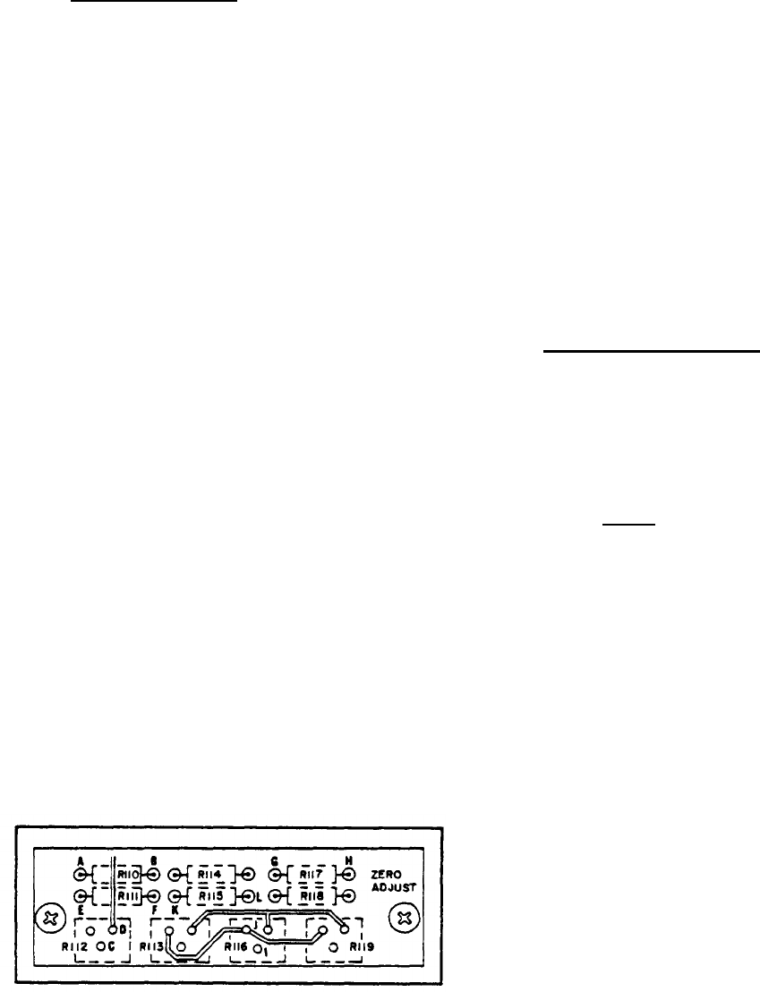
5-81 CONSTANT VOLTAGE PROGRAMMING
CURRENT
5-82 Zero Output Voltage. To calibrate the zero
voltage programming accuracy, proceed as direct-
ed in Paragraphs 5-83, 5-84, 5-85, or 5-86,
whichever applies to your particular instrument.
5-83 Standard instrument with resistance or unity-
gain voltage programming.
a. Connect differential voltmeter between
+OUT and -OUT bus bars.
b. If unit is to be used in local program-
ming mode, turn VOLTAGE controls fully counter-
clockwise. If unit is to be used in remote pro-
gramming mode, connect remote programming setup
(Figure 3-3 or 3-4) and adjust remote resistance or
voltage to zero (minimum).
c. Connect decade resistance box between
pads of position marked for resistor R110 in “ZERO
ADJUST” section of main circuit board (points “A”
and “B” in Figure 5-10; also see Figure 7-10).
d. Rotate CURRENT controls fully clockwise
and turn on supply.
e.Adjust decade resistance box until dif-
ferential voltmeter reads exactly zero volts.
f. Replace decade resistance box with
fixed, metal film, 1%, 1/4 or 1/8 watt resistor of
same value.
5-84 Standard instrument with non-unity gain
voltage programming.
a. Perform Steps (a) and (b) in Paragraph
5-83. b. Solder jumper between “wiper” pad and
“+12.4V” pad of position marked for potentiometer
R112 in “ZERO ADJUST” section of main circuit
board (points “C” and “ D“ in Figure 5-10; also
see Figure 7-10).
c. Connect decade resistance box between
pads marked for resistor R111 in “ZERO ADJUST”
section of main circuit board (points “ E“ and “ F“
in Figure 5-10; also see Figure 7-10).
d. Perform Steps (d) through (f) in Paragraph
5-83.
Figure 5-10. “ZERO ADJUST” Section of Main
circuit Board
5-85 Option 020 with resistance or unity-gain
TM 11-6625-2958-14&P
voltage programming.
a. Perform Steps (a) and (b) in Paragraph
5-83. b. Rotate CURRENT controls fully clockwise
and turn on supply.
c. If reading on differential 1 voltmeter is not
exactly zero volts, adjust potentiometer R113 (la-
beled "VOLTAGE ZERO" and accessible through
hole in’ rear panel) until reading is exactly zero.
5-86 Option 020 with non-unity gain voltage pro-
gramming.
a.
Perform Steps (a) and (b) in Paragraph
5-83. b. Rotate CURRENT controls fully clockwise
and turn on supply.
c. If reading on differential voltmeter is not
exactly zero volts, adjust potentiometer R112 (la-
beled “VOLTAGE PROG” and accessible through
hole in rear panel) until reading is exactly zero.
5-87 CV Programming Accuracy. To caIibrate the
constant voltage programming current, proceed as
directed in Paragraphs 5-88 or 5-89, whichever
applies to your particular instrument.
5-88 Standard instrument.
a. Connect 0.1%, 1/8 watt resistor of value
shown below between terminals -S and A3 on rear
barrier strip. Model
Value
62596
2K Ω
62606
2K Ω
62616
4K Ω
6268B
8K Ω
62696
8K Ω
b. Disconnect strap between terminals Al
and A2 on rear barrier strip.
c. Connect differential voltmeter between
+OUT and -OUT bus bars.
d. Connect decade resistance box in place
of R3 (mounted on standoffs on main circuit board;
see Figure 7-10).
e.
Rotate CURRENT controls fully clockwise
and turn on supply.
f. Adjust decade resistance box until dif-
ferential voltmeter indicates exactly maximum
rated output voltage.
g. Replace decade resistance box with
fixed, composition, 5%, 1/2 watt resistor of same
vaIue.
5-89 Option 020.
a.
Perform Steps (a) through (c) in Paragraph
5-88. b. Rotate CURRENT controls fully clockwise
and turn on supply.
c. Adjust potentiometer R112 (labeled
“VOLTAGE PROG” and accessible through hole in
rear panel) until differential voltmeter indicates
5-19

TM 11-6625-2958-14&P
exactly maximum rated output voltage.
5-90 CONSTANT CURRENT PROGRAMMING
CURRENT
5-91 Zero Current OutPut. To calibrate the zero
current programming accuracy, proceed as direct-
ed in Paragraphs 5-92, 5-93, 5-94, or 5-95,
whichever applies to your particular instrument.
5-92 Standard instrument with resistance or
unity-gain voltage programming.
a.
Connect test setup shown in Figure 5-8.
b. If unit is to be used in local program-
ming mode, turn CURRENT controls fully counter-
clockwise. If unit is to be used in remote pro-
gramming mode, connect remote programming setup
(Figure 3-6 or 3-7) and adjust remote resistance or
voltage to zero. (minimum).
c. Connect decade resistance box between
pads of position marked for resistor R117 in “ZERO
ADJUST” section of main circuit board (points “G”
and “H” in Figure 5-10; also see Figure 7-10).
d. Rotate VOLTAGE controls fully clockwise
and turn on supply.
e.
Adjust decade resistance box until dif-
ferential voltmeter reads exactly zero volts.
f. Replace decade resistance box with
fixed, metal film, 1%, 1/4 or 1/8 watt resistor of
same value.
5-93 Standard instrument with non-unity gain
voltage programming.
a.
Perform Steps (a) and (b) in Paragraph
5-92. b. Solder jumper between “wiper” pad and
“-6.2V” pad of position marked for potentiometer
R116 in “ZERO ADJUST” section of main circuit
board (points “I” and “J” in Figure 5-10; also see
Figure 7-10).
c. Connect decade resistance box between
pads marked for resistor R115 in “ZERO ADJUST”
section of main circuit board (points “ K“ and “ L“
in Figure 5-1 O; also see Figure 7-10).
d.
Perform Steps (d) through (f) in Paragraph
5-92.
5-94 Option 021 with resistance or unity-gain
voltage programming.
a.
Perform Steps (a) and (b) in Paragraph
5-92. b. Rotate VOLTAGE controls fully clockwise
and turn on supply.
c. If reading on differential voltmeter is
not exactly zero volts, adjust potentiometer R119
(labeled “CURRENT ZERO” and accessible through
hole in rear panel) until reading is exactly zero.
5-95 Option 021 with non-unity gain voltage pro-
gramming.
a.
Perform Steps (a) and (b) in Paragraph
5-92.
b. Rotate VOLTAGE controls fully clockwise
and turn on supply.
c. If reading on differential voltmeter is not
exactly zero volts, adjust potentiometer R116 (la-
beled “CURRENT PROG” and accessible through
hole in rear panel) until reading is exactly zero.
5-96 CC Programming Accuracy. To calibrate the
constant current programming current, proceed as
directed in Paragraphs 5-97 or 5-98, whichever
applies to your particular instrument.
5-97 Standard instrument.
a. Connect test setup shown in Figure 5-8.
b, Disconnect strap between terminals A5
and A6 on rear barrier strip.
c. Connect 0.1%, 1/8 watt resistor of value
shown below between terminals A4 and A6 on rear
barrier strip.
Mode 1
Value
6259B
200
Ω
6260B
200
Ω
6261B
200
Ω
6268B
180
Ω
6269B
200
Ω
d. Connect decade resistance box in place
of R30 (mounted on standoffs on main circuit
board; see Figure 7-1 O).
e.
Rotate VOLTAGE controls fully clockwise
and turn on supply.
f. Adjust decade resistance box until dif-
ferential voltmeter indicates exactly 0.5Vdc.
9.
Replace decade resistance box with
fixed, composition, 5%, 1/2 watt resistor of same
value.
5-98 Option 021.
a.
Perform Steps (a) through (c) in Paragraph
5-97. b. Rotate VOLTAGE controls fully clockwise
and turn on supply.
c. Adjust potentiometer R116 (labeled “CUR-
RENT PROG” and accessible through hole in rear
panel) until differential voltmeter indicates exactly
0.5Vdc.
5-99 TRANSIENT RECOVERY TIME
5-100 To adjust the transient response, proceed
as follows:
a.
Connect test setup shown in Figure 5-5.
b. Repeat Steps (a) through (k) as outlined
in Paragraph 5-32.
c. Adjust R47 until transient response is
within specification as shown in Figure 5-6.
5-101 RIPPLE IMBALANCE (50 and 60Hz Operation)
5-102 This procedure ensures balanced operation
of the triac by ensuring that the conduction time
5-20

TM 11-6625-2958-14&P
is equal in either direction (within 25%). To check
for imbalance, proceed as follows:
a.
Connect appropriate Ioad resistance
across rear output terminals of supply as follows:
MODEL
Load Resistance
6259B
0.2 Ω 500W, ±5%
6260B
O.1 Ω, 1000W, ±5%
62610
0.4
Ω, 1000W, ±5%
6268B
1.33 Ω, 1200W, ±5%
6269B
0.8 Ω, 2000W, ±5%
b. Connect variable auto transformer be-
tween input power source and power supply power
input; adjust auto transformer for 230Vac input to
supply.c. Connect oscilloscope (ac coupled) be-
tween TP102 and TP103 (across series regulator).
d. Turn CURRENT controls fully clockwise,
turn on supply, and adjust VOLTAGE controls for
maximum rated output voltage.
e. Adjust oscilloscope to observe 120Hz
sawtooth waveform. Peak amplitudes of adjacent
sawtooth peaks should be within 25% of each other.
f. If amplitude difference is greater than
25%, turn off supply and replace R82 with decade
resistance.
9.
Turn on supply and adjust decade resist-
ance to reduce imbalance to within 25%.
h. Vary input line voltage from 207 to 253V
ac and insure that imbalance does not exist any-
where within this range. Replace decade box with
equivalent resistor.
NOTE
If imbalance cannot be reduced to
within 25%, check capacitors C70 and
C72, and diodes CR79 through CR84.
If these components test satisfactori-
ly, the problem may be due to distor-
tion present on the ac power line.
5-103 PREREGULATOR TRACKING (50 and 60Hz
Operation)
5-104 To adjust the voltage drop across the series
regulator, proceed as follows:
a. Connect appropriate load resistance
across rear output terminals of supply as follows:
Model Load Resistance
62S9B
0.2
Ω500W, ±5%
6260B
0.1 Ω, 1000W, ±5%
6261B
0.4
Ω, 1000W, ±5%
6268B
1.33
Ω,
1200W, ±5%
6269B
0.8
Ω,
2000W, ±5%
b. Connect variable auto transformer be-
tween input power source and power supply power
input adjust auto transformer for 230Vac input to
supply.
Connect dc voltmeter acress series reg-
ulator (TP102 and TP103).
d. Turn CURRENT controls fully clockwise.
e,
To check voltage drop across regulator
at low output voltage, short circuit load resistor
and adjust VOLTAGE controls for maximum rated
output current on front pane 1 ammeter.
f. Adjust R70 until voltmeter reads 3.5±
0.3Vdc.
g. To check the voltage drop at high output
voltage, remove short circuit from acress load re-
sistor and adjust VOLTAGE controls for maximum
rated output current. Voltmeter reading should
again be 3.5 ± 0.3Vdc.
h. Vary input line voltage from 207 to 253V
ac. Voltmeter reading should vary between 3.2
(minimum) and 3.8 (maximum) volts. If reading ex-
ceeds this range, proceed with Step (i).
i.Replace resistor R77 with decade resis-
tance box. Vary input line voltage between 207
and 253Vac while adjusting decade box until volt-
meter reading variation is minimal and within range
of 3.2 to 3.8Vdc. Rep lace decade box with equiv-
alent resistor.
5-105 50Hz OPERATION (Option 005)
5-106 If the supply is to be operated from a 50Hz
ac input, the following modifications are required:
a. Replace resistor R82 with 240 Ω, ±5%,
1/2 watt resistor, and check ripple imbalance as
described in Steps (a) through (e) of Paragraph
5-101. b. Perform preregulator tracking adjustment
described in Paragraph 5-103.
5-107 CROWBAR TRIP VOLTAGE
5-108 To adjust A5R125 (OVERVOLTAGE ADJUST),
proceed as follows:
.Turn screwdriver adjustment, A5R125,
fully clockwise.
b. Turn on supply.
c. Set voltage output to desired trip voltage.
d. Turn A5R125 slowly counterclockwise
until the crowbar is tripped (meter falls to zero
volts). e. Turn off supply and turn down output
voltage.
f. Turn on supply and set desired operating
output voltage.
NOTE
It is recommended that the crowbar be
set to no less than 5% of the desired
output voltage plus two volts, in or-
der to avoid false tripping of the
crowbar. However, if occasional
crowbar tripping on unloading can be
tolerated, the crowbar trip point can
5-21

TM 11-6625-2958-14&P
be set much closer to the operating
output voltage of the supply.
5-109 MAXIMUM CROWBAR TRIP VOLTAGE
5-110 To adjust the maximum voltage at which the
crowbar trips, proceed as follows:
a. Rotate A5R125 (OVERVOLTAGE ADJUST)
and CURRENT controls fully clockwise.
b. Disconnect either end of R72 (TP70 or
TP71; see Figure 7-10).
c. Connect decade resistance box in place
of R95 (mounted on standoffs on main circuit
board). d. Turn on supply and adjust VOLTAGE con-
trols for output voltage shown below:
Model Value
6259B 12Vdc
6260B 12Vdc
Model Value
6261B 23Vdc
6268B 45Vdc
6269B 45Vdc
e.
Adjust decade resistance box until crow-
bar trips (amber OVERVOLTAGE lamp lights up).
f. Replace decade resistance with appro-
priate value resistor in R95 position and reconnect
resistor R72. Maximum crowbar trip voltage is
now set at voltage given in Step (d).
5-111 CROWBAR DISABLEMENT
5-112 To disable the crowbar completely, discon-
nect either end of R98 (TP97 or TP98). This resis-
tor is mounted on the main circuit board (see Fig-
ure 7-10).
5-22

TM 11-6625-2958-14&P
SECTION VI
REPLACEABLE PARTS
6-1 INTRODUCTION
6-2 This section contains information for ordering
replacement parts. Table 6-4 lists parts in alpha-
numeric order by reference designators and provides
the following information:
a.
Reference Designators. Refer to Table 6-1.
b. Description. Refer to Table 6-2 for ab-
breviations.
c. Total Quantity (TQ). Given only the first
time the part number is listed except in instruments
containing many sub-modular assemblies, in which
case the TQ appears the first time the part number
is listed in each assembly.
d. Manufacturer’s Part Number or Type.
e.
Manufacturer’s Federal Supply Code Num-
ber. Refer to Table 6-3 for manufacturer’s name and
address.
f. Hewlett-Packard Part Number.
g. Recommended Spare Parts Quantity (RS)
for complete maintenance of one instrument during
one year of isolated service.
h. Parts not identified by a reference desig-
nator are listed at the end of Table 6-4 under Me-
chanical and/or Miscellaneous. The former consists
of parts belonging to and grouped by individual as-
semblies; the latter consists of all parts not im-
mediately associated with an assembly.
6-3 ORDERING INFORMATION
6-4 Table 6-5 is a part number-national
stock number cross reference index.The
items on this cross reference index are
source coded PAHZZ. Items that do not
appear on this cross reference index are
source coded XD and shall be procured
using the FSCM and the NPN at the near-
est wholesale level.
Table 6-1. Reference Designators
A
= assembly
E
= miscellaneous
B
= blower (fan) electronic part
C
= capacitor
F = fuse
CB
= circuit breaker J= jack, jumper
CR
= diode
K
= relay
DS
= device, signal- L= inductor
ing (lamp) M= meter
Table 6-1. Reference Designators (Continued)
P
= plug
Q
= transistor
R
= resistor
s= switch
T
= transformer
TB
= terminal block
TS
= therms 1 switch
v. vacuum tube,
neon bulb,
photocell, etc.
VR
= zener diode
x= socket
z= integrated cir-
cuit or network
Table 6-2. Description Abbreviations
A
= ampere
ac
= alternating
current
ass y.
= assembly
bd
= board
bkt = bracket
°C
= degree
Centigrade
cd = card
coef = coefficient
comp
= composition
CRT
= cathode-ray
tube
CT
= center-tapped
dc
= direct current
DPDT = double pole,
double throw
DPST = double pole,
single throw
elect = electrolytic
encap =
encapsulated
F
= farad
OF
= degree
Farenheit
fxd = fixed
Ge
= germanium
H
= Henry
Hz
= Hertz
IC
= integrated
circuit
ID = inside diameter
incnd = incandescent
k= kilo =103
m
= mini = 10-3
M
= mega = 106
µ= micro = 10-6
met.
= metal
mf r
= manufacturer
mod.
= modular or
modified
mtg
= mounting
n= nano =10-9
NC
= normally closed
NO
= normally open
NP
= nickel-plated
W
= ohm
obd
= order by
description
OD
= outside
diameter
p= pico =10-12
P.C. = printed circuit
pot. = potentiometer
P-P
= peak-to-peak
ppm
= parts per
million
pvr = peak reverse
voltage
rect = rectifier
rms
= root mean
square
S1
= silicon
SPDT = single pole,
double throw
SPST = single pole,
single throw
SS
= small signal
T
= slow-blow
tan. = tantulum
T1
= titanium
V
= volt
var = variabIe
ww
= wirewound
w= Watt
6-1

TM 11-6625-2958-14&P Table 6-3. Code List of Manufacturers
CODE
NO.
MANUFACTURER
ADDRESS
00629
EBY Sales Co. , Inc. Jamaica, N. Y.
00656
Aerovox Corp.
New Bedford, Mass.
00853
Sangamo Electric Co.
S. Carolina Div.
Pickens, S. C.
01121
Allen Bradley Co. Milwaukee, Wis.
01255
Litton Industries, Inc. Beverly Hills, Caltf.
01281
TRW Semiconductors, Inc.
Lawndale, Calif.
01295
Texas Instruments, Inc.
Semiconductor-Components Div.
Dallas, Texas
01686
RCL Electronics, Inc. Manchester, N. H.
01930
Amerock Corp.
Rockford, 111.
02107
Sparta Mfg. Co. Dover, Ohio
02114
Ferroxcube Corp.
Saugerties, N. Y.
02606
Fenwal Laboratoriess
Morton Grove, Ill.
02660
Amphenol Corp.
Broadview, Ill.
02735
Radio Corp. of America, Solid State
and Receiving Tube Div. Somerville, N. J.
03508
G. E. Semiconductor Products Dept.
Syracuse, N. Y.
03797
Eldema Corp.
Compton, Calif.
03877
Transitron Electronic Corp.
Wakefield, Mass.
03888
Pyrofilm Resistor Co. Inc.
Cedar Knolls, N. J.
04009
Arrow, Hart and Hegeman Electric Co.
Hartford, Corm.
04072
ADC Electronics, Inc. Harbor City, Calif,
04213
Caddell & Bums Mfg. Co. Inc.
Mineola, N. Y.
04404
*Hewlett-Packard Co. Palo Alto Div,
Palo Alto, Calif,
04713
Motorola Semiconductor Prod. Inc.
Phoenix, Arizona
05277
Westinghouse Electric Corp.
Semiconductor Dept. Youngwood, Pa.
05347
Ultronix, Inc. Grand Junction, Colo.
05820
Wake field Engr. Inc. Wakefield, Mass.
06001
General Elect, Co. Electronic
Capacitor & Battery Dept. Irmo, S. C.
06004
Bassik Div. Stewart-Warner Corp.
Bridgeport, Corm.
06486
IRC Div. of TRW Inc.
Semiconductor Plant
Lynn, Mass.
06540
Amatom Electronic Hardware Co. Inc.
New Rochelle, N. Y.
06555
Beede Electrical Instrument Co.
Penacook, N. H.
06666
General Devices Co. Inc.Indianapolis, Ind.
06751
Semcor Div. Components, Inc.
Phoenix, Arizona
06776
Robinson Nugent, Inc. New Albany, Ind.
06812
Torrington Mfg. Co. , West Div.
Van Nuys, Calif.
07137
Transistor Electronics Corp.
Minneapolis, Minn.
CODE
NO. MANUFACTURER
ADDRESS
07138
Westinghouse Electric Corp.
Electronic Tube Div. Elmira, N. Y.
07263
Fairchild Camera and Instrument
Corp. Semiconductor Div.
Mountain View, Calif.
07387
Birtcher Corp-,The Los Angeles, Calif.
07397
Sylvania Electric Prod. Inc.
Sylvania Electronic Systems
Western Div. Mountain View, Calif.
07716
IRC Div. of TRW Inc. Burlington Plant
Burlington, Iowa
07910
Continental Device Corp.
Hawthorne, Calif.
07933
Raytheon Co. Components Div.
Semiconductor Operation
Mountain View, Calif.
08484
Breeze Corporations, Inc. Union, N. J.
08530
Reliance Mica Corp. Brooklyn, N. Y.
08717
Sloan Company, The
Sun Valley, Calif.
08730
Vemaline Products Co. Inc. Wyckoff, N. J.
08806
General Elect. Co. Minia-
ture Lamp Dept. Cleveland, Ohio
08863
Nylomatic Corp. Norrisville, Pa.
08919
RCH Supply Co.
Vernon, Calif.
09021
Airco Speer Electronic Components
Bradford, Pa.
09182
*Hewlett-Packard Co. New Jersey Div.
Rockaway, N. J.
09213
General Elect. Co. Semiconductor
Prod. Dept. Buffalo, N. Y.
09214
General Elect. Co. Semiconductor
Prod. Dept. Auburn, N. Y.
09353
C & K Components Inc. Newton, Mass.
09922
Burndy Corp.
Norwalk, Corm.
11115
Wagner Electric Corp.
Tung-Sol Div. Bloomfield, N. J.
11236
CTS of Berne, Inc. Berne, Ind.
11237
Chicago Telephone of Cal. Inc.
So. Pasadena, Calif.
11502
IRC Div. of TRW Inc. Boone Plant
Boone, N.C.
11711
General Instrument Corp
Rectifier Div.
Newark, N. J.
12136
Philadelphia Handle Co. Inc.Camden, N. J.
12615
U. S. Terminals, Inc. Cincinnati, Ohio
12617
Hamlin Inc. Lake Mills, Wisconsin
12697
Clarostat Mfg. Co. Inc. Dover, N. H.
13103
Thermally Co. Dallas, Texas
14493
*Hewlett-Packard Co. Loveland Div.
Loveland, Colo.
14655
Comell-Dubilier Electronics Div.
Federal Pacific Electric Co. Newark, N. J.
14936
General Instrument Corp. Semicon-
ductor Prod. Group Hicksville, N. Y.
15801
Fenwal Elect.
Framingham, Mass.
16299
Corning Glass Works, Electronic
Components Div.
Raleigh, N. C.
*Use Code 28480 assigned to Hewlett-Packard Co. , Palo Alto, California
6-2

TM 11-6625-2958-14&P
Table 6-3. Code List of Manufacturers (Continued)
.
CODE
NO.
MANUFACTURER
ADDRESS
16758
Delco Radio Div. of General Motors Corp.
Kokomo, I.nd.
17545
Atlantic Semiconductors, Inc.
Asbury Park, N. J.
17803
Fairchild Camera and Instrument Corp
Semiconductor Div. Transducer Plant
Mountain View, Callf.
17870
Daven Div. Thomas A. Edison Industries
McGraw-Edison Co. Orange, N. J.
18324
Slgnetics Corp. Sunnyvale, Callf.
19315
Bendix Corp. The Navigation and
Control Div.
Teterboro, N. J.
19701
Electra/Midland Corp.
Mineral Wells, Texas
21520
Fansteel Metallurgical Corp.
No. Chicago, Ill.
22229
Union Carbide Corp. Electronics Div.
Mountain View, Calif.
22753
UID Electronics Corp. Hollywood, Fla.
23936
Pamotor, Inc.
Pampa, Texas
24446
General Electric Co. Schenectady, N.Y.
24455
General Electric Co. Lamp Div. of Con-
sumer Prod. Group
Nela Park, Cleveland, Ohio
24655
General Radio Co.
West Concord, Mass.
24681
LTV Electrosystems Inc Memcor/Com-
ponents Operations
Huntington, Ind.
26982
Dynacool Mfg. Co. Inc. Saugerties, N.Y.
27014
National Semiconductor Corp.
Santa Clara, Callf.
28480
Hewlett-Packard Co. Palo Alto, Calif.
28520
Heyman Mfg. Co. Kenilworth, N. J.
28875
IMC Magnetics Corp.
New Hampshire Div. Rochester, N. H.
31514
SAE Advance Packaging, Inc.
Santa Ana, Callf.
31827
Budwig Mfg. Co. Ramona, Calif.
33173
G. E. Co. Tube Dept.
Owensboro, Ky.
35434
Lectrohm, Inc. Chicago, Ill.
37942
P. R. Mallory & Co. Inc. Indianapolis, Ind.
42190
Muter Co.
Chicago, 111.
43334
New Departure-Hyatt Bearings Div.
General Motors Corp.
Sanclusky, Ohio
44655
Ohmite Manufacturing Co.
Skokie, 111.
46384
Penn Engr. and Mfg. COrp.Doylestown, Pa.
47904
Polaroid Corp.
Cambridge, Mass.
49956
Raytheon Co.
Lexington, Mass.
55026
Simpson Electric Co. Div. of American
Gage and Machine Co.
Chicago, 111.
56289
Sprague Electric Co. North Adams, Mass.
58474
Superior Electrlc Co. Bristol, Corm.
58849
Syntron Div. of FMC Corp. Homer City, Pa.
59730
Thomas and Betts Co.
Philadelphia, Pa.
61637
Union Carbide Corp. New York, N. Y.
63743
Ward Leonard Electric Co.
Mt. Vernon, N. Y.
CODE
NO.
MANUFACTURE R ADDRESS
70563
Amperite Co. Inc. Union City, N. J.
70901
Beemer Engrg. Co.
Fort Washington, Pa.
70903
Belden Corp.
Chicago, III.
71218
Bud Radio, Inc. Willoughby, Ohio
71279
Cambridge Thermionic Corp.
Cambridge, Mass.
71400
Bussmann Mfg. Div. of McGraw &
Edison Co.
St. Louis, Mo.
71450
CTS Corp.
EIkhart, Ind.
71468
I. T. T. Cannon Electric Inc.
Los Angeles, Callf.
71590
Globe-Union Inc.
Centralab Div. Milwaukee, Wis.
71700
General Cable Corp. Cornish
Wire Co. Div. Williams town, Mass.
71707
Coto Coil Co. Inc.
Providence, R. 1.
71744
Chicago Miniature Lamp Works
Chicago, Ill.
71785
Cinch Mfg. Co. and Howard
B. Jones Div. Chicago, III.
71984
Dow Coming Corp. Midland, Mich.
72136
Electro Motive Mfg. Co. Inc.
Willimantic, Corm.
72619
Dialight Corp. Brooklyn, N. Y.
72699
General Instrument Corp.
Newark, N. J.
72765
Drake Mfg. Co. Harwood Heights, Ill.
72962
Elastic Stop Nut Div. of
Amerace Esna Corp.
Union, N. J.
72982
Erie Technological Products Inc. Erie, Pa.
73096
Hart Mfg. Co. Hartford, Corm.
73138
Beckman Instruments Inc.
Helipot Div. Fullerton, Calif.
73168
Fenwal, Inc. Ashland, Mass.
73293
Hughes Aircraft Co. Elecmon
Dynamics Div. Torrance, Calif.
73445
Amperex Electronic Corp.
Hicksville, N, Y.
73506
Bradley Semiconductor Corp.
New Haven, Corm.
73559
Carling Electric, Inc. Hartford, Corm.
73734
Federal Screw Products, Inc. Chicago, Ill.
74193
Heinemann Electric Co.
Trenton, N. J.
74545
Hubbell Harvey Inc.
Bridgeport, Corm.
74868
Amphenol Corp. Amphenol RF Div.
Danbury, Corm.
74970
E. F. Johnson Co.
Waseca, Minn.
75042
IRC Div. of TRW, Inc. Philadelphla, Pa.
75183
l Howard B. Jones Div. of Cinch
Mfg. Corp.
New York, N. Y.
75376
Kurz and Kasch, Inc. Dayton, Ohio
75382
Kilka Electric Corp. Mt. Vernon, N. Y.
75915
Llttlefuse, Inc. Des Plaines, Ill.
76381
Minnesota Mining and Mfg. Co.
St. Paul, Minn.
76385
Minor Rubber Co. Inc. Bloomfield, N.J.
76487
James Millen Mfg. Co. Inc.
Maiden, Mass.
76493
J. W. Miller Co. Compton, Callf.
l Use Code 71785 assigned to Cinch Mfg. Co. , Chicago, III.
6-3

TM 11-6625-2958-14&P Table 6-3. Code List of Manufacturers (Continued)
CODE
NO. MANUFACTURER
ADDRESS
76530
Cinch City of Industry, Calif.
768.54
Oak Mfg. Co. Div. of Oak
Electro/Netics Corp. Crystal Lake, III.
77068
Bendix Corp. , Electrodynamics Div.
No. Hollywood, Calif.
77122
Palnut Co.
Mountainside, N. J.
77147
Patton -Mac Guyer Co.
Providence, R. I.
77221
Phaostron Instrument and Electronic Co.
South Pasadena, Calif.
77252
Philadelphia Steel and Wire Corp.
Philadelphia, Pa.
77342
American Machine and Foundry Co.
Potter and Brumfield Div. Princeton, Ind.
77630
TRW Electronic Components Div.
Camden, N. J.
77764
Resistance Products Co.
Harrisburg, Pa.
78189
Illinois Tool Works Inc. Shakeproof Div.
Elgin, Ill.
78452
Everlock Chicago, Inc.
Chicago, 111.
78488
Stackpole Carbon Co.
St. Marys, Pa.
78526
Stanwyck Winding Div. San Fernando
Electric Mfg. Co. Inc. Newburgh, N.Y.
78553
Tinnerman Products, Inc. Cleveland, Ohio
78584
Stewart Stamping Corp.
Yonkers, N. Y.
79136
Waldes Kohinoor, Inc. L.I.C., N.Y.
79307
Whitehead Metals Inc. New York, N. Y.
79727
Continental-Wirt Electronics Corp.
Philadelphia, Pa.
79963
Zierick Mfg. Co. Mt. Kisco, N.Y.
80031
Mepco Div. of Sessions Clock Co.
Morristown, N. J.
80294
Bourns, Inc. Riverside, Calif.
81042
Howard Industries Div. of Msl Ind. Inc.
Racine, Wise.
81073
Grayhiil, Inc. La Grange, III.
81483
International Rectifier Corp.
El Segundo, Calif.
81751
Columbus Electronics Corp. Yonkers, N. Y.”
82099
Goodyear Sundries & Mechanical Co. Inc.
New York, N. Y.
82142
Airco Speer EIectronic Components
Du Bois, Pa.
82219
Sylvania Electric Products Inc.
Electronic Tube Div. Receiving
Tube Operations Emporium, Pa.
82389
Switchcraft, Inc. Chicago, Ill.
82647
Metals and Controls Inc. Control
Products Group
Attleboro, Mass.
82866
Research Products Corp.
Madison, Wis.
82877
Rotron Inc.
Woodstock, N. Y.
82893
Vector Electronic Co. Glendale, Calif.
83058
Cam Fastener Co.
Cambridge, Mass.
83186
Victory Engineering Corp. Springfield, N. J.
83298
Bendix Corp. Electric Power Div.
Eatontown, N, J.
83330
Herman H. Smith, Inc. Brooklyn, N. Y.
83385
Central Screw Co. Chicago, Ill.
83501
Gavitt Wire and Cable Div. of
Amerace Esna Corp.
BrookfieId, Mass.
CODE
NO. MANUFACTURER
ADDRESS
83508
Grant Pulley and Hardware Co.
West Nyack, N. Y.
83594
Burroughs Corp. Electronic
Components Div.
Plainfield, N.J.
83835
U. S. Radium Corp.
Morristown, N.J.
83877
Yardeny Laboratoriess, Inc.
New York, N.Y.
84171
Arco Electronics, Inc. Great Neck, N.Y
84411
TRW Capacitor Div. Ogallala, Neb.
86684
RCA Corp. Electronic Components
Harrison, N. J.
86838
Rummel Fibre Co.
Newark, N, J.
87034
Marco & Oak Industries a Div. of Oak
Electro/netics Corp. Anaheim; Calif.
87216
Philco Corp. Lansdale Div. Lansdale, Pa.
87585
Stockwell Rubber Co. Inc.Philadelphia, Pa.
87929
Tower-Olschan Corp. Bridgeport, Corm.
88140
Cutler-Hammer Inc. Power Distribution
and Control Div. Lincoln Plant
Lincoln, III.
88245
Litton Precision Products Inc, USECO
Div. Litton Industries Van Nuys, Calif.
90634
Gulton Industries Inc. Metuchen, N,J.
90763
United-Car Inc. Chicago, III.
91345
Miller Dial and Nameplate Co.
El Monte, Calif.
91418
Radio Materials Co. Chicago, Ill.
91506
Augat, Inc. Attleboro, Mass.
91637
Dale Electronics, Inc. Columbus, Neb.
91662
Elco Corp.
Willow Grove, Pa.
91929
Honeywell Inc. Div. Micro Switch
Freeport, Ill.
92825
Whitso, Inc. Schiller Pk. , III.
93332
Sylvania Electric Prod. Inc. Semi-
conductor Prod. Div. Woburn, Mass.
93410
Essex Wire Corp. Stemco
Controls Div. Mansfield, Ohio
94144
Raytheon Co. Components Div.
Ind. Components Oper. Quincy, Mass.
94154
Wagner Electric Corp.
Tung-Sol Div. Livingston, N. J.
94222
Southco Inc.
Lester, Pa.
95263
Leecraft Mfg. Co. Inc. L.I.C., N.Y.
95354
Method Mfg. Co. Rolling Meadows, III,
95712
Bendix Corp. Microwave
Devices Div. Franklin, Ind.
35987
Weckesser Co. Inc. Chicago, Ill.
96791
Amphenol Corp. Amphenol
Controls Div. Janesville, Wis.
97464
Industrial Retaining Ring Co.
Irvington, N.J.
97702
IMC Magnetics Corp. Eastern Div.
Westbury, N. Y.
98291
Sealectro Corp. Mamaroneck, N. Y.
98410
ETC Inc.
Cleveland, Ohio
38978
‘International Electronic Research Corp.
Burbank, Calif.
39934
Renbrandt, Inc. Boston, Mass.
6-4

Table 6-4. Replaceable Parts TM 11-6625-2958-14&P
REF.
DESCRIPTION MFR.
HP
DESIG.
TQ
MFR. PART NO.
CODE
PART NO.
RS
Al MAIN PRINTED CIRCUIT BOARD
A1
Printed Circuit Board, Main 1
28480
5060-6189
C1
fxd, mylar. 01µF 200V 1
28480
0160-0161
1
C2
fxd, elect. 5µF 50Vdc 3
30D505G050BB2 56289
0180-0301
1
C20
fxd, elect. 68µF 15Vdc 2
150D686X0015R2 56285
0180-1835
1
C35
fxd, elect. 20µF 50Vdc 1
30 D206G050C02
C40, 41 56289
0180-0049
1
fxd, mylar .022µF 200Vdc 2
192P22392 56289
0160-0162 1
C44
fxd, elect. 1,400µF 30Vdc 1
28480
0180-1860 1
C60
fxd, elect. 4.7µF 35Vdc 1
150D475X9035B2 56289
0180-0100 1
C61
fxd, elect. 325µF 35Vdc 1
28480
0180-0332 1
C70
fxd, elect. 1µF 35Vdc 1
150D105X9035A2 56289
0180-0291
1
C71
fxd, mylar .1µF 200Vdc 2
192P10492 56289
0160-0168
C72, 73
1
fxd, elect. 5µF 50Vdc
30D505G050BB2 56289
.0180-0301
C90
fxd, mylar .1µF 200Vdc
192P10492 56289
0160-0168
CR1-7,20,
21,35-37 Diode, Si. 200mA 200prv
38
28480
1901-0033
12
CR40
Stabistor 1
28480
1901-0460
1
CR41,43,44 Diode, Si 200mA 200prv
28480
1901-0033
CR42,51,52
NOT ASSIGNED
- -
CR45-50,
53,54 Diode, Si. 8
1N5059
CR60-62,
03508
1901-0327
6
70-84,88,
90-93 Diode, Si. 200mA 200prv
28480
1901-0033
Q1
SS PNP Si. 6
Q20, 40 28480
1853-0099
6
SS NPN Si. 9
28480
1854-0071
6
Q41, 42
SS PNP Si.
28480
1853-0099
Q60
SS PNP Si 1
28480
1853-0041
1
Q61-Q63
SS NPN Si.
28480
1854-0071
Q70, 71
SS PNP Si.
28480
1853-0099
Q72, 73
SS NPN Si.
28480
1854-0071
Q90
SS PNP Si.
28480 1853-009-9
Q91, 92
SS NPN Si.
09182
1854-0071
R1
fkd, met. film 1M Ω ±1% ¼ Ω1Type CEB T-O
07716
0757-0344 1
R2
fxd, comp 160 Ω ±5% ½ Ω2
EB-1615
01121
0686-1615
1
R3
fxd, comp (selected) +5% ½ Ω2
Type EB (obd)
01121
-1
R4
fxd, ww 680 Ω ±5%5W 1
243E6815 56289
0811-2099
1
R5
fxd, ww 600Ω ±5%5W1
243E6015 56289
0811-1869 1
R6
fxd, ww 1K
Ω
± 5% 3W
1
242E1025 56289
0813-0001
1
R20
fxd, met. film 330 Ω ±1% 1/8W 1Type CEA T-0
07716
0698-5663
1
R21
fxd, met. film 200k Ω ±1% 1/8W 1Type CEA T-0
07716
0757-0472
1
R22
fxd, met. film 196 Ω ±1% 1/8W 1Type CEA T-0
07716
0698-3440 1
R23
fxd, met. film 1.21k Ω ±1% 1/8W 2Type CEA T-0
07716
0757-0274 1
R24
fxd. met. film 7.5K Ω ±1% 1/8W 3Type CEA T-0
07716
0757-0440 1
R25
fxd, met. film 5.49K
Ω
±1% 1/8W
2Type CEA T-0
077,16
0698-3382 1
R26
fxd, met. film 21.5K Ω ±1% 1/8W 1Type CEA T-0
07716
0698-3430 1
R27
fkd, comp 3.9M Ω ±5%½W 1
EB-3955
01121
0686-3955
1
R28, 29
fxd, comp 3.3
Ω
±5%½W
2
EB-0335
01121
0686-0335
1
R30
fxd, comp (Selected) ±5%½W
Type EB (obd)
01121
-
R31
fxd, ww 2.6K
Ω
±5% 3W
1
242E2625 56289
0811-1808
1
R35, 36
fxd, compp 10k Ω ±5%½W2
EB-1035
01121
0686-1035
1
R37
fxd, comp 180k Ω ±5%½W1
EB-1845
01121
0686-1845
1
R40
fxd, comp 1.5K
Ω
±5%½W
1
EB-1525
01121
0686-1525
1
62690
6-5

REF.
MFR.
HP
DESIG. DESCRIPTION
TQ
MFR. PART NO.
CODE
PART NO.
RS
R41
fxd, comp 510
Ω
±5% ½W
2
EB-5115
01121
0686-5115 1
R42
fxd, met. film 560 Ω ±1% ¼W 1Type CEB T-O
07716
0698-5146 1
R43
fxd, ww 50 Ω ±5% 5W 2
243E5005
56289
0811-1854 1
R44
fxd, met. oxide 22 Ω ±5% 2W 1
Type C42S
16299
0698-3609 1
R45
fxd, comp 820
Ω
±5% ½W
1
EB-8215
01121
0686-8215 1
R46
fxd, comp 1K
Ω
±5% ½W
2
EB-1025
01121
0686-1025 1
R47
var. ww 5k Ω ±10%, Equalizer Adj. 2Type 110-F4
11236
2100-1824 1
R48
fxd, comp 5.1k Ω ±5% ½W 1
EB-5125
01121
0686-5125 1
R49
fxd, comp 47
Ω
±5% ½W
1
EB-4705
01121
0686-4705 1
R50
fxd, comp 39
Ω
±5% ½W
1
EB-3905
01121
0686-3905 1
R51
fxd, comp 1k
Ω
±5% ½W EB-1025
01121
0686-1025
R52
fxd, met. film 61.9k Ω ±1% 1/8W 1Type CEA T-O
07716
0757-0460 1
R53
fxd, comp 560
Ω
±5% ½W
1
EB-5615
01121
0686-5615 1
R54
fxd, ww 50 Ω ±5% 5W
243 E5005
56289
0811-1854
R56
fxd, comp 75
Ω
±5% ½W
1
EB-7505
01121
0686-7505 1
R57
fxd, ww 3.9 Ω 2W 1
Type BWH
07716
0811-1673 1
R58
fxd, ww 400 Ω ±5% 10W 1
Type 10XM
63743
0811-0942 1
R60
fxd, met. film 600 Ω ±1% 1/8W 1Type CEA T-O
07716
0757-1100 1
R61
fxd, met. film 7.5K Ω ±1% 1/8W Type CEA T-O
07716
0757-0440
R62
fxd, met. oxide 180 Ω ±5% 2W 1
Type C42S
16299
0698-3626 1
R63
fxd, met. film 499 Ω ±1% ¼W 1Type CEB T-O
07716
0698-3207 1
R64
fxd, met. film 2k Ω ±1% ¼W 1Type CEB T-O
07716
0757-0739 1
R65
fxd, comp I00kW ±5% ½W 2
EB-1045
01121
0686-1045 1
R66
fxd, comp 200k Ω ±5% ½W 3
EB-2045
01121
0686-2045 1
R67
fxd, comp 33k
Ω
±5% ½W
1
EB-3335
01121
0686-3335 1
R68
fxd, met. film 5.49k Ω ±1% 1/8W Type CEA T-O
07716
0698-3382
R69
fxd, met. film 7.5k Ω ±1% 1/8W Type CEA T-O
07716
0757-0440
R69B
fxd, met. film 3.4k Ω ±1% 1/8W 1Type CEA T-O
07716
0698-4440 1
R70 var, ww 5k Ω ±10%, Ramp Adjust. Type 110-F4
11236
2100-1824
R71
fxd, met. film 12k Ω ±1% 1/8W 1Type CEA T-O
07716
0698-5088 1
R72
fxd, met. film 45k Ω ±1% 1/8W 1Type CEA T-O
07716
0698-5091 1
R73
fxd, comp 12k
Ω
±5% ½W
1
EB-1235
01121
0686-1235 1
R74
fxd, comp 82k
Ω
±5% ½W
1
EB-8235
01121
0686-8235 1
R75, 76
fxd, met. film 4,75k Ω ±1% 1/8W 2Type CEA T-O
07716
0757-0437 1
R77
fxd, comp 430k
Ω
±5% ½W
1
EB-4345
01121
0686-4345 1
R78
fxd, met. film 249k Ω ±1% 1/8W 1Type CEA T-O
07716
0757-0270 1
R79
fxd, comp 3.9k Ω ±5% ½W 2
EB-3925
01121
0686-3925 1
R80
fxd, met. film 4.32k Ω ±1% 1/8W 1Type CEA T-O
07716
0757-0436 1
R81
fxd, comp 4.7 Ω ±5% ½W 2
EB-47G5
01121
0698-0001 1
R82
fxd, comp 9.1k Ω ±5% ½W 2
EB-9125
01121
0686-9125 1
R83
fxd, comp 27
Ω
±5% ½W
1
EB-2705
01121
0686-2705 1
R84
fxd, comp 100k
Ω
±5% ½W EB-1045
01121
0686-1045
R85
fxd, comp 9.1k Ω ±5% ½W
EB-9125
01121
0686-9125
R86
fxd, met. oxide 270 Ω ±5% 2W 1
Type C42S
16299
0698-3629 1
R87
fxd, met. oxide 1.5k Ω ±5% 2W1
Type C42S
16299
0698-3338 1
R88
fxd, comp 10
Ω
±5% ½W
2
EB-1OO5
01121
0686-1005 1
R90 fxd, met. oxide 820 Ω ±5% 2W 1
Type C42S
16299
0698-3637 1
R91
fxd, comp 180 Ω ±5% 1W 1
GB-1815
01121
0689-1815 1
R92
fxd, ww 220 Ω 2W 1
Type BWH
07716
0811-1763 1
R93
fxd, comp 3.9k Ω ±5% ½W
EB-3925
01121
0686-3925
R94
fxd, comp 510
Ω
±5% ½W EB-5115
01121
0686-5115
R95
fxd, met. film 1.5k Ω ±1% 1/8W 2Type CEA T-O
07716
0757-0427 1
R96
fxd, comp 200k
Ω
±5% ½W EB-2045
01121
0686-2045
R97
fxd, comp 4.7 Ω ±5% ½W
EB-47G5
01121
0698-0001
R98
fxd, comp 10
Ω
±5% ½W EB-1005
01121
0686-1005
R99
fxd, comp 200k Ω ±5% ½W
EB-2045
01121
0686-2045
R101
var. ww 250 Ω ±10%, Ammeter Adj. 2Type 110-F4
11236
2100-0439 1
R102
fxd, met. film 909 Ω ±1% 1/8W 1Type CEA T-O
07716
0757-0422 1
6269B
6-6
TM11-6625-2958-14&P

REF.
MFR.
HP
DESIG. DESCRIPTION
TQ
MFR. PART NO.
CODE
PART NO.
RS
R103
fxd, met. film 1.5k Ω ±1% 1/8W Type CEA 7-0
07716
0757-0427
R104
fxd, met. film 19.1k Ω ±1% 1/8W 1Type CEA T-O
07716
0698-4484 1
R105
fxd, met. film 422 Ω ±1% ¼W 1Type CEB T-O
07716
0698-4590 1
R106
var. ww 250 Ω ±10%, Voltmeter Adj. Type 110-F4
11236
2100-0439
R108, 109
fxd, comp 100
Ω
±5% ½W
2
EB-1015
01121
0686-1015
1
T70, 90
Pulse Transformer 2
28480
5080-7122 1
VR1, 40
Diode, zener 4.22V ±5% 2
28480 1902-.3070
2
VR60, 61
Diode, zener 6.2V ±5% 2
28480
1902-1221
2
VR90
Diode, zener 6.19V ±5% 1
28480
1902-0049
1
Z1
Dual Differential Amplifier 1
CA3026
02735
1820-0240 1
22
Resistor Network 1
28480
1810-0042 1
A2 RFI FILTER ASSEMBLY
A2
RFI Filter Assembly 1
28480
06269-60007
C1
fxd, paper .22µF 600Vdc 1
Type 160P 56289
0160-2461
1
CR1
Triac, 40A 400prv 1
2N5445 02735
1884-0080
1
L1A/L1B
Filter Choke 1.5mH 1
28480
5080-7146 1
R1
fxd, met. oxide 270 Ω ±5% 2W 1
Type C42S
16299
0698-3629 1
A3 INTERCONNECTION BOARD
A3
Interconnection Board Assembly 1
28480
5060-7906
C3
fxd, elect. 5000µF 45Vdc 1
28480
0180-1919
1
J1
P.C. Board Edge Connector 164-718-22
76530
1251-1887
R120
fxd, comp 51k
Ω
±5% ½W
1
EB-5135
01121
0686-5135
1
T2
Bias Transformer 1
28480
9100-26O7
1
A4 HEAT SINK ASSEMBLY
A4
Heat Sink Assembly 1
28480
06269-60004
B1
Fan
1
WS2107F
97702
3160-0056
1
C1-C4 fxd, ceramic .05µF 400V 4
28480
0150-0052 1
C5
fxd, elect. 15µF 50V 1
28480
0180-1834 1
CR101, 102
4
1N1183AR 02577
1901-0316
4
Rect. Si. 40A 50prv
CR103, 104
Rect. Si. 40A 50prv 3
1N1183A 02577
1901-0315
3
CR1O5
Rect. Si. 40A 50prv
1N1183AR 02577
CR106
1901-0316
Rect. Si. 40A 50prv
1N1183A 02577
1901-0315
CR108
Rect. Si. 40A 50prv
1N1183AR 28480
1901-0316
CR110
SCR 35A 4ooprv
1
28480
1884-0058
1
Q101
Power PNP Si.
1
28480
1853-0063
1
Q102
Power NPN Si.
1
28480
1854-022S
1
Q103-Q108
Power NPN Si. 6
28480
1854-0458
6
R106
fxd, ww .125 Ω ±5% 5W 1
28480
0811-1846 1
R123
fxd, cupron 0.01 Ω 20ppm, Cur-
rent Sampling 1
28480
5080-7144 1
R150-R155
Emitter Resistor Assembly 1
28480
06260-60023 1
fxd, wire helix O.1 Ω ±5% - Part of
Emitter Resistor Assembly 6
28480
0811-2545
2
6269B
6-7
TM 11-6625-2958-14&P

REF.
MFR. HP
DESIG. DESCRIPTION
TQ
MFR. PART NO.
CODE
PART NO.
RS
TS101
Thermal Switch, open 230°F, close
200°F
1
28480
0440-0079 1
A5 FRONT PANEL ASSEMBLY
A5
Front Panel Assembly 1
28480
06269-60005
CB1
Circuit Breaker, 25A @ 250Vac max. 1AM33 Curve 5
74193
2110-0213 1
DS1
Indicator Light, Neon, Red 1599-124
72765
1450-0048 1
DS2
Overvoltage Indicator, 6V, Amber 1MCL-A3-1730
07137
1450-0305 1
MlVoltmeter, 0-50V 1
28480
1120-1173 1
M2
Ammeter, 0-60A 1
28480 1120-1181
1
R121
var. ww 10k Ω ±5%, Voltage
Control, Coarse 2
28480
2100-1854 1
R122
var. ww 50 Ω ±5%, Voltage
Control, Fine 2
28480
2100-1858 1
R123
var. ww 200 Ω ±5%, Current
Control, Coarse 1
28480
2100-1856 1
R124
var. ww 10 Ω ±5%, Current
Control, Fine 1
28480
2100-1857 1
R125
var. ww 10k Ω ±5%, Overvoltage
Adjustment
28480
2100-1854
CHASSIS - ELECTRICAL
B2
Fan
1
8500 23936
3160-0056 1
C19
fxd, elect. 15µF 50Vdc 1
150D156X0050R2
56289
0180-1834 1
C101-C104 fxd, elect. 50,000µF 50Vdc 4
28480
0180-2346 1
C110, 111
fxd, ceramic .01µF 300Vdc 2
41C21A5
56289
0160-2568 1
T1
Power Transformer 1
28480
06269-80091 1
CHASSIS ASSEMBLY- MECHANICAL
Chassis Assembly (Welded) 1
28480
5060-6186
Bracket, RFI Filter Mounting 2
28480
5000-6257
Standoff, Insulated, RFI Filter
Mounting 4
28480
0380-0902
Grommet, 5/8” (Internal
Chassis Divider) 1
1661
73734
0400-0062
Cover 2
28480
5000-6250
Chassis, Internal, Ckt. Board Tray 1
28480
5000-6248
Chassis, Internal, Capacitor Tray 1
28480
06269-00002
Bus Bar, C101-C102 2
28480
5000-6251
Bus Bar, C103-C104 2
28480
5000-6253
Clamp, C101-C104 3
28480
5000-6017
Bracket, Fan B2 2
28480
06269-00003
Rear Panel (Blank, with labeling) 1
28480
06260-60008
Cover, AC Input Barrier Block 1
28480
5000-6249
Cover, Rear Control Barrier Strip 1
28480
00712-20001
Bus Bar, Output 2
28480
5000-6252
Barrier Block, AC Input 1603-3
75382
0360-1596 1
Rubber Bumper
42097-W
87585
0403-0089
Spacer, Insulated, AC Input
Barrier (2), Output Bus Bars (4) 6
28480
0380-0710 6
Serial I.D. Plate 1
28480
7120-1111
6269B
6-8
TM 11-6625-2958-14&P

TM 11-6625-2958-14&P
REF.
MFR.
HP
DESIG. DESCRIPTION
TQ
MFR. PART NO.
CODE
PART NO.
RS
Shoulder Washer, Bus Bar 4
28480
2190-0491
4
Binding Post, 5 Way, N. P. Brass
(Ground)
1
137
83330
1510-0044
Al- MECHANICAL
Barrier Strip, Rear Control 1
28480
0360-1518
1
Jumper, Barrier Strip 4422-13-11-013
71785
0360-1143 2
A2 - MECHANICAL
Heat Sink, RFI Filter Ass’y. (CRl) 1
28480
5020-5785
Cover, RFI Assembly 1
28480
5020-5768
Terminal, Insulated, Cl 1
28480
0360-1449 1
Wafer, Insulated, CR1 1
28480
0340-0175
1
Shoulder Washer, CR1 1
28480
2190-0898 1
Hole Plug, Heat Sink, 7/8” dia. 1
28480
6960-0047 1
A3-MECHANICAL
Clamp, Capacitor, C3 1
28480
1400-0472
1
A4 -MECHANICAL
Heat Sink, Q103-104-107-108,
Q105-106 2
28480
5020-5763
Heat Sink, CR101-103, CR102-104 2
28480
5020-5769
Heat Sink, CR106,108,Q102 1
28480
5020-5766
Heat Sink, CR105, CR110,Q101 1
28480
5020-5765
Bracket, Mounting, Fan-Heat Sink 1
28480
5000-6256
Bracket, Mtg. Heat Sink-Chassis 1
28480
5000-6255
Insulator Strip, Heat Sink Divider 2
28480
5020-5787 1
Washers, Nylon, Heat Sink Spacing
12
28480
3050-0455
3
Rod, Insulated Spacing, 8-3/4 Lg.,
Threaded 6-32 4
8203-PH0632
‘ 06540 0380-0879 1
Rubber Bumper, Heat Sink Protection 1
28480
0403-0002 1
Insulator, Mica, Q101-102 2
734 08530
0340-0174 2
Shoulder Washer, Q101-102 4
28480
2190-0490
4
Insulator, Transistor Pins, Q101-110
16
28480
0340-0166 8
Insulator, Mica, CR109 1
28480
2190-0709
1
Shoulder Washer, CR109 1
28480
2190-0898
1
Shoulder Washer, Heat Sink Bracket
Mounting 4
28480
3050-0483 4
AS -MECHANICAL
Front Panel (Blank) 1
28480
5000-6254
Knob, Front Panel, Black 4
28480
0370-0137
1
Fastener, DS1, DS2 2C17373-012-248
89032
0510-0123
Bushing, Potentiometer R125 1
28480
1410-0052
1
Nut, Hexagon, R125 1
28480
2950-0034
Locknut, R121-R124 4
28480
0590-0013
Bezel, Gray Plastic, 2¼" Mod. 2
28480
4040-0296 1
Spring, M1, M2 8
28480
1460-0256
2
Handle, 7“ 2
28480
5020-5762
Machine Screw, Fillister Phillips
Head, 10-32x 1-3/4 4
28480
2680-0173
6269B
6-9

TM 11-6625-2958-14&P
TQ
MFR. PART NO.
1
1
2
REF.
DESIG.
I
DESCRIPTION
MISCELLANEOUS
Manual
Carton, Packing
Floater Pad, Packing
28480 06269-90002
28480 9211-1181
28480
9220-1402
OPTION 005
50Hz Operation
1
1
1
1
1
01121
0686-2415
7124-1719
R82
fxd, comp 240
Ω
±5% ½W
Label, Identification 1
EB-2415
1
OPTION 007
10-Turn Voltage Coarse Control
28480
2100-1866
A5R121
var. ww 10k Ω ±5% 10-Turn 1 I
28480
2100-1863
OPTION 008
10-Turn Current Coarse Control
A5R123
var. ww 200 Ω ±5% 10-Turn 1
1
1
OPTION 009
10-Turn Voltage & Current Controls
A5R121
A5R123
var. ww 10k Ω ±5% 10-Turn
var. ww 200 Ω ±5% 10-Turn
28480
2100-1866
28480
2100-1863
OPTION 010
Chassis Slides
Slides, Chassis 1
1 CTS 120 E6
1
Type EB (obd)
1
OPTION 013
Decadial Voltage Control
R3
A5R121
fxd, comp (Selected) ±5% ½W
var. ww 10k Ω ±5% 10-Turn
Decadial Control
01121
28480
2100-1866
07716
1140-0020 1
1
1 RD-411
OPTION 014
Decadial Current Control
01121
28480
2100-1863
07716
1140-0020
fxd, comp (Selected) ±5% ½W
var. ww 200 Ω ±5% 10-Turn
Decadial Control
1
Type EB (obd)
1
1
RD-411
R30
A5R123
1
1
1
1
1
07716
0757-0473
28480
2100-0806
07716
0757-0270
7124-1721
OPTION 020
Voltage Programming Adjust
fxd, met. film 221k Ω ±1% 1/8W
var. ww 5k Ω
fxd, met. film 249k Ω ±1% 1/8W
Label, Identification
1Type CEA T-O
2
1Type CEA T-O
1
R111
R112,113
R114
OPTION 021
Current Programming Adjust
1Type CEA T-O
2
07716
0698-3269
28480
2100-0806
07716
0757-0472
28480
2100-0806
7124-1721
1
1
1
fxd, met. film 23K Ω ±1% 1\8W
var. ww 5k Ω
fxd, met. film 200k Ω ±1% 1/8W
var. ww 5k Ω
Label, Identification
R115
R116
R118
R119
6269B
6-10
1
1
Type CEA T-O
MRF.
CODEHP
PART NO.
RS
TM 11-6625-2958-14&P
REF DESCRIPTION TQ MFR HP RS
DESIGN MFR PART NO CODE PART NO
OPTION 022
VOLTAGE & CURRENT PROGRAMMING ADJUST
R111 FXD, MET. FILM 221KW ±1% 1/8W 1TYPE CEA T-O 07716 0757-0473 1
R112,113 VAR. WW 5K
Ω
4 28480 2100-0806 1
R114 FXD, MET. FILM 249KW ±1% 1/8W 1TYPE CEA T-O 07716 0757-0270 1
R115 FXD, MET. FILM 23KW ±1% 1/8W 1TYPE CEA T-O 07716 0698-3269 1
R116 VAR. WW 5K
Ω
28480 2100-0806
R118 FXD, MET. FILM 200KW ±1% 1/8W 1TYPE CEA T-O 07716 0757-0472 1
R119 VAR. WW 5KW 28480 2100-0806
LABEL, IDENTIFICATION 1 28480 7124-1721
OPTION 027
208VAC INPUT
LABEL, IDENTIFICATION 1 28480 7124-1717
6269B
6-11
TM11-6625-2958-14&P TABLE 6-5. PART NUMBER - NATIONAL STOCK NUMBER
CROSS REFERENCE INDEX
NATIONAL NATIONAL
PART STOCK PART STOCK
NUMBER FSCM NUMBER NUMBER FSCM NUMBER
0150-0052 28480 5910-00-797-4909 0757-0437 28480 5905-00-904-4404
0160-0161 28480 5910-00-911-9271 0757-0440 28480 5905-00-858-6795
0160-0162 28480 5910-00-850-2162 0757-0460 28480 5905-00-858-8959
0160-0168 28480 5910-00-917-0668 0757-0472 28480 5905-00-257-9210
0180-0049 28480 5910-00-781-9398 0757-0473 28480 5905-00-994-8480
0180-0100 28480 5910-00-752-4172 0757-0739 28480 5905-00-830-6078
0180-0291 28480 5910-00-931-7055 0757-1100 28480 5905-00-917-0586
0180-0332 28480 5910-00-943-6709 0813-0001 28480 5905-00-932-0413
0180-1860 28480 5910-00-931-7061 1N5059 03508 5961-00-088-8792
0686-1035 28480 5905-00-451-0540 1140-0020 28480 5355-00-584-0840
0686-1045 28480 5905-00-195-6761 1251-1887 28480 5935-00-147-7384
0686-1525 28480 5905-00-279-1757 137 83330 5940-00-321-4984
0686-3335 28480 5905-00-997-5436 1410-0052 28480 5895-00-061-2906
0686-4345 28480 5905-00-279-2518 1450-0048 28480 6210-00-761-8898
0686-5125 28480 5905-00-279-2019 150D105X9035A2 56289 5910-00-104-0144
0689-1815 28480 5905-00-403-9066 150D475X9035B2 56289 5910-00-177-4300
0698-0001 28480 5905-00-682-4247 1661 73734 5325-00-301-8656
0698-3338 28480 5905-00-431-6842 1810-0042 28480 5905-00-450-0107
0698-3430 28480 5905-00-420-7136 1853-0041 28480 5961-00-931-8259
0698-3440 28480 5905-00-828-0377 1853-0063 28480 5961-00-867-9319
0698-3629 28480 5905-00-405-3727 1853-0099 28480 5961-00-450-4689
0698-4440 28480 5905-00-431-6840 1854-0071 28480 5961-00-137-4608
0698-4484 28480 5905-00-140-5675 1854-0225 28480 5961-00-072-0094
0698-5088 28480 5905-00-469-2838 1901-0033 28480 5961-00-821-0710
0698-5146 28480 5905-00-431-6837 1901-0327 28480 5961-00-931-0213
0757-0270 28480 5905-00-491-4596 1901-0460 28480 5961-00-867-9206
0757-0274 28480 5905-00-858-9105 1902-0049 28480 5961-00-911-9277
0757-0344 28480 5905-00-269-2629 1902-3070 28480 5961-00-931-6989
0757-0422 28480 5905-00-728-9980 192P10492 56289 5910-00-728-8472
0757-0427 28480 5905-00-917-0578 192P22392 56289 5910-00-993-8308
0757-0436 28480 5905-00-858-6792 2100-0439 28480 5905-00-851-3924
6-12
PART NUMBER - NATIONAL STOCK NUMBER TM 11-6625-2958-14&P
CROSS REFERENCE INDEX
NATIONAL NATIONAL
PART STOCK PART STOCK
NUMBER FSCM NUMBER NUMBER FSCM NUMBER
2100-0806 28480 5905-00-929-0485
2100-1824 28480 5905-00-892-9626
2100-1857 28480 5905-00-575-8853
2100-1866 28480 5905-00-110-0282
242E1025 56289 5905-00-504-4892
243E5005 56289 5905-00-950-5551
2950-0034 28480 5310-00-903-8729
30D505G050BB2 56289 5910-00-081-6159
3160-0056 28480 4140-00-758-6113
422-13-11-013 71785 5935-00-917-9079
599-124 72765 6210-00-761-8898
734 08530 5970-00-840-5109
6-13
TM 11-6625-2958-14&P
SECTION Vll
CIRCUIT DIAGRAMS AND COMPONENT LOCATION DIAGRAMS
This section contains the circuit diagrams neces- b. Preregulator control circuit waveforms
sary for the operation and maintenance of this (Figure 7-9), showing the waveforms found at vari-
power supply. Included are: ous points in the preregulator control circuit.
a.
Component location diagrams (Figures 7-1 c. Schematic diagram (Figure 7-1 1), illustrat-
through 7-8, and 7-10), showing the physical loca- ing the circuitry for the entire power supply. Volt-
tion and reference designators of parts mounted on ages are given adjacent to test points, which are
the printed circuit boards and chassis. identified by encircled numbers on the schematic.
7-1
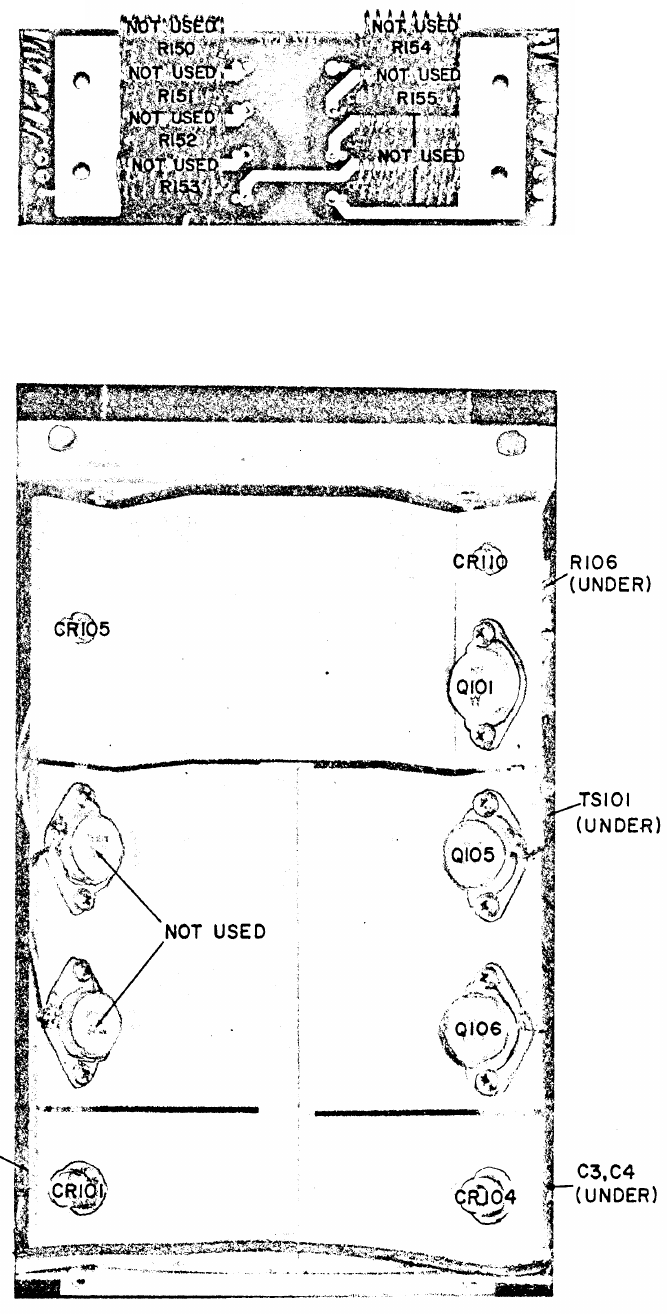
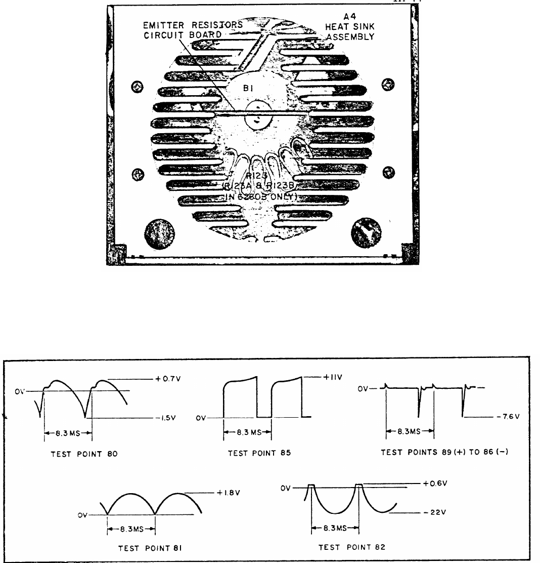
Figure 7-8.A4 Heat Sink Assembly Component Location Diagram
(End view, assembly removed from supply.)
1. ALL WAVEFORMS TAKEN AT MAXIMUM RATED OUTPUT VOLTAGE, 230 VAC INPUT, NO LOAD CONNECTED AND
CURRENT CONTROLS FULLY CLOCKWISE.
2. SCOPE DC COUPLED AND REFERENCED TO TP103 (INBOARD SIDE OF CURRENT SAMPLING RESISTOR) UNLESS
OTHERWISE SHOWN.
3. FOR CLARITY, WAVEFORMS ARE NOT DRAWN TO SCALE.
Figure 7-9. Preregulator Control Circuit Waveforms
7-7
TM 11-6625-2958-14&P
NOTES

Figure 7-10
This publication does not contain Figure 7-10.
Figure 7-10 does not exist in paper or digital form.
NOT DIGITIZED

DA Pam 310-4
DA Pam 310-7
TM 38-750
TM 740-90-1
TM ‘750-244-2
TB 43-180
TB 385-4
TM 11-6625-2958-14&P
APPENDIX A
REFERENCES
Index of Technical Manuals, Technical Bulletins,
Supply Manuals (Types 7, 8 and 9), Supply
Bulletins,and Lubrication Orders.
Index of Modification Work Orders.
The Army Maintenance Management System (TAMMS).
Administrative Storage of Equipment.
Procedures for Destruction of Electronics Materiel
to Prevent Enemy Use (Electronics Command).
Calibration Requirements for the Maintenance of
Army Materiel.
Safety Precautions for Maintenance of Electrical/
Electronic Equipment.
A-1

TM 11-6625-2958-14&P
APPENDIX B
COMPONENTS OF END ITEM LIST
Section L INTRODUCTION
B-1.
Scope
This appendix lists integral components of and
basic issue items for the PP-7545/U to help
you inventory items required for safe and efficient
operation.
B-2. General
.This Components of End Item List is divided into
the following sections:
a. Section II. Integral Components of the End
item. Not applicable. The-se items, when assem-
bled, comprise the PP-754.5/U and must accom-
pany it whenever it is transferred or turned in.
The illustrations will help you identify these items.
b. Section III. Basic Issue Items. Not applicable.
These are the minimum essential items required
to place the PP-7545/U in operation, to operate
it, and to perform emergency repairs. Although
shipped separately packed they must accompany
the PP-7545/U during operation and whenever
it is transferred between accountable officers. The
illustrations will assist you with hard-b-identify
items. This manual is your authority to requisition
replacement BII, base don TOE/MTOE authoriza-
tion of the end item.
B-3. Explanation of Columns
a. Illustration. This column is divided as fol-
lows :
(1) Figure number. Indicates the figure num-
.ber of the illustration on which the item is shown.
(2) Item number. The number used to iden-
tify item called out in the illustration.
b. National Stock Number. Indicates the Na-
tional stock number assigned to the item and
which will be used for requisitioning.
c. Description. Indicates the Federal item name
and, if required, a minimum description to iden-
tify the item. The part number indicates the pri-
mary number used by the manufacturer, which
controls the design and characteristics of the item
by means of its. engineering drawings, specifica-
tions, standards, and inspection requirements to
identify an item or range of items. Following the
part number, the Federal Supply Code for Manu-
facturers (FSCM) is shown in parentheses
d. Location The physical location of each item
listed is given in this column. The lists are de-
signed to inventory all items in one area of the
major item before moving on to an adjacent area.
e. Usable on Code. Not applicable.
f. Quantity Required (Qty Reqd). This column
lists the quantity of each item required for a
complete major item.
g. Quantity. This column is left blank for use
during an inventory. Under the Rcvd column, list
the quantity you actually receive on your major
item. The Date columns are for your use when you
inventory the major item.
(Next printed page is B-2.)
B-1
SECTION II INTEGRAL COMPONENTS OF END ITEM TM 11-6625-2958-14&P
SECTION III BASIC ISSUE ITEMS
(1) (2) (3) (4) (5) (6) (7)
ILLUSTRATION NATIONAL DESCRIPTION LOCATION USABLE QTY QUANTITY
(A) (B) STOCK ON REQD
FIG ITEM NUMBER CODE RCVD DATE
NO NO PART NUMBER (FSCM)
1-1 N/A 6130-00-148-1796 PP-7545/U 28480 1
TM 11-6625-2958-14&P 1
B-2

TM 11-6625-2958-14&P
APPENDIX D
MAINTENANCE ALLOCATION
Section L INTRODUCTION
D-1. General
This appendix provides a summary of the main-
tenance operations for the PP-7545/U. It
authorizes categories of maintenance for specific
maintenance functions on repairable items and
components and the tools and equipment required
to perform each function. This appendix may
be used as an aid in planning maintenance opera-
tions.
D-2. Maintenance Function
Maintenance functions will be limited to and de-
fined as follows:
a. Inspect. To determine the serviceability of an
item by comparing its physical, mechanical, and/
or electrical characteristics with established stand-
ards through examination.
b. Test. To verify serviceability and to detect
incipient failure by measuring the mechanical or
electrical characteristics of an item and compar-
ing those characteristics with prescribed stand-
ards.
c. Service. Operations required periodically to
keep an item in proper operating conditions, i.e.,
to clean (decontaminate), to preserve, to drain,
to paint, or to replenish fuel, lubricants, hydraulic
fluids, or compressed air supplies.
d. Adjust To maintain, within prescribed limits,
by bringing into proper or exact position, or by
setting the operating characteristics to the speci-
fied parameters.
e. Align To adjust specified variable elements
of an item to bring about optimum or desired
performance.
f. Calibrate. To determine and cause corrections
to be made or to be adjusted on instruments or
test measuring and diagnostic equipments used
in precision measurement. Consists of compari-
sons of two instruments, one of which is a certified
standard of known accuracy, to detect and adjust
any discrepancy in the accuracy of the instrument
being compared.
g. install. The act of emplacing, seating, or fix-
ing into position an item, part, module (compo-
nent or assembly) in a manner to allow the proper
functioning of the equipment or system.
h. Replace. The act of substituting a serviceable
like type part, subassembly, or module (component
or assembly) for an unserviceable counterpart.
i. Repair. The application of maintenance serv-
ices (inspect, test, service, adjust, align, calibrate,
replace) or other maintenance actions (welding,
grinding, riveting, straightening, facing, rema-
chining, or resurfacing) to restore serviceability
to an item by correcting, specific damage, fault,
malfunction, or failure in a part, subassembly,
module (component or assembly), end item, or
system.
j. Overhaul. That maintenance effort (service/
action) necessary to restore an item to a complete-
ly serviceable/operational condition as prescribed
by maintenance standards (i.e., DMWR) in appro-
priate technical publications. Overhaul is normally
the highest degree of maintenance performed by
the Army. Overhaul does not normally return an
item to like new condition.
k. Rebuild. Consists of those services actions
necessary for the restoration of unserviceable
equipment to a like new condition in accordance
with original manufacturing standards. Rebuild
is the highest degree of materiel maintenance
applied to Army equipment. The rebuild operation
includes the act of returning to zero those age
measurements (hours, miles, etc. ) considered in
classifying Army equipments/components.
D-1
TM 11-6625-2958-14&P
D-3. Column Entries
u. Column 1, Group Number. Column 1 lists
group numbers, the purpose of which is to identify
components, assemblies, subassemblies, and mod-
ules with the next higher assembly.
b. Column 2, Component/Assembly. Column 2
contains the noun names of components, assem-
blies, subassemblies, and modules for which main-
tenance is authorized.
c. Column 3, Maintenance Functions. Column 3
lists the functions to be performed on the item
listed in column 2. When items are listed without
maintenance functions, it is solely for purpose
of having the group numbers in the MAC and
RPSTL coincide.
d. Column 4, Maintenance Category. Column 4
specifies, by the listing of a “worktime” figure in
the appropriate subcolumn (s), the lowest level of
maintenance authorized to perform the function
listed in column 3. This figure represents the ac-
tive time required to perform that maintenance
function at the indicated category of maintenance.
If the number or complexity of the tasks within
the listed maintenance function vary at different
maintenance categories, appropriate “worktime”
figures will be shown for each category. The num-
ber of task-hours specified by the “worktime”
figure represents the average time required to
restore an item (assembly, subassembly, compo-
nent, module, end item or system) to a serviceable
condition under typical field operating conditions.
This time includes preparation time, troubleshoot-
ing time, and quality assurance/quality control
time in addition to the time required to perform
the specific tasks identified for the maintenance
functions authorized in the maintenance allocation
chart. Subcolumns of column 4 are as follows:
C - Operator/Crew
0- Organizational
F - Direct Support
H - General Support
D - Depot
e. Column 5, Tools and Equipment. Column 5
specifies by code, those common tool sets (not
individual tools) and special tools, test, and sup-
port equipment required to perform the designated
function.
f. Column 6, Remarks. Column 6 contains an
alphabetic code which leads to the remark in
section IV, Remarks, which is pertinent to the
item opposite the particular code.
D-4. Tool and Test Equipment Requirement
(sect Ill)
a. Tool or Test Equipment Reference Code. The
numbers in this column coincide with the numbers
used in the tools and equipment column of the
MAC. The numbers indicate the applicable tool
or test equipment for the maintenance functions.
b. Maintenance Category. The codes in this
column indicate the maintenance category allo-
cated the tool or test equipment.
c. Nomenclature. This column lists the noun
name and nomenclature of the tools and test
equipment required to perform the maintenance
functions.
d. National/NATO Stock Number. This column
lists the National, NATO stock number of the
specified tool or test equipment.
e. Tool Number. This column lists the manu-
facturer’s part number of the tool followed by the
Federal Supply Code for manufacturers (5-digit)
in parentheses.
D-5. Remarks (sect IV)
a. Reference Code. This code refers to the ap-
propriate item in section II, column 6.
b. Remarks. This column provides the required
explanatory information necessary to clarify items
appearing in section II.
D-2
TM11-6625-2958-14&P SECTION III TOOL AND TEST EQUIPMENT REQUIREMENTS
FOR
POWER SUPPLY PP-7545/U
TOOL OR TEST
EQUIPMENT MAINTENANCE NOMENCLATURE NATIONAL/NATO TOOL NUMBER
REF CODE CATEGORY STOCK NUMBER
1 O MULTIMETER AN/URM-105 6625-00-581-2036
2 O TOOL KIT, ELECTRONIC EQUIPMENT TK-101/G 5180-00-064-5178
3H, D TOOL KIT, ELECTRONIC EQUIPMENT TK-105/G 5180-00-610-8177
4H, D GENERATOR, SIGNAL SG-321/U 6625-00-880-5791
5H, D MULTIMETER, AN/USM-223/U 6625-00-999-7465
6H, D MULTIMETER, ELECTRONIC, ME-260/U 6625-00-913-9781
7H, D OSCILLOSCOPE AN/USM-281 6625 00-106-9622
8H, D RESISTANCE BRIDGE, ZM-4()/U 6625-00-500-9370
9H, D TRANSFORMER, VARIABLE CN-16/U 5950-00-235-2086
10 H, D VOLTMETER DIGITAL, AN/GSM-64 6625-00-022-7894
11 H, D VOLTMETER DIGITAL, ME-202/U 6625-00-709-0288
D-4

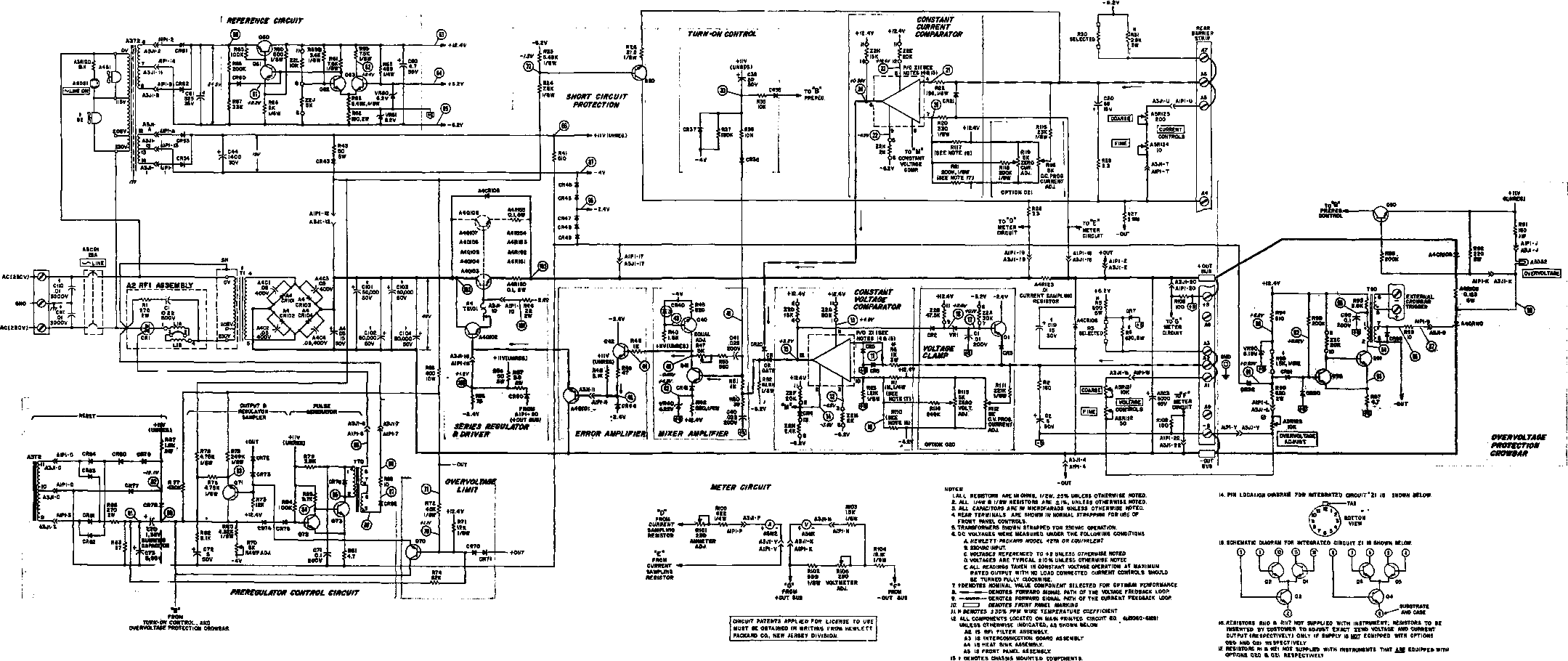

MANUAL CHANGES
Model 6269B DC Power Supply
Manual HP Part No. 06269-90002
Make all corrections in the manual according to errata below, then check the following table for your power
supply serial number and enter any listed” change(s) in the manual.
SERIAL
Prefix
ALL
1027A
1027A
1027A
1027A
1027A
1027A
1027A
1027A
1027A
1027A
1436A
1506A
1513A
1535A
Number
0245, 0246,
0255
0236, 0239,
0241 - 0244,
0247, 0248,
0252 -0254,
0256-0305
0306 - 0355
0356 - 0380
0381 - 0429
0430 - 0455
0456 - 0540
0541
- 0870
0871
- 1080
1081
- 1260
1261
- 1470
1471
- 1510
1511
- 1630
1631
- up
MAKE
CHANGES
Errata
1
1,2
1,2,3
1,2, 3,4
1 thru S
1 thru 6
1 thru 7
1 thru 8
1 thru 9
1 thru10
1 thru 11
1 thru 12
1 thru 13
1 thru 14
ERRATA:.
In the Replaceable Parts List, make the following
changes:
Knob, front panel, black: Change to HP Part No.
0370-0084.
Option 007: Add knob, HP Part No. 0370-0137,
quantity 1.
Option 008: Add knob, HP Part No. 0370-0137,
quantity 1.
Option 009: Add knob, HP Part No. 0370-0137,
quantity 2.
Under AS-Mechanical:
Bezel, Gray Plastic: Change to HP Part No.
4040-0293 (Black).
Under Chassis Assembly-Mechanical
Bus Bar, C103-C104: Change to HP Part No.
5000-6251.
CHANGE 1:
Add new RC network (C2 and R2) on the RFI filter
board assembly A2.
On the schematic, C2 and R2
are connected directly across Triac CR1 (C2 is on
the inboard side of CR1).
C2 and R2 prevent the misfiring (turning on too
soon) of triac CR1 by slowing the rate of voltage
increase across L1A/B (in series with T1) when
the triac turns off.
In the Replaceable Parts list under AZ RFI Filter
Assembly:
C2: Add, 0.047µF, 600V, HP Part No. 0160-0005.
R2: Add, 220 Ω, ±5%, 2W, HP Part No. 0811-1763.
In the Replaceable Parts Iist, make the following
changes:
CR1: Delete Mfr. Part No. and change HP Part
No. to 1884-0209.
Under A2-Mechanical:
Wafer, Insulated, CR1: Delete.
Shoulder Washer, CR1: Delete.
CHANGE 2:
In the Replaceable Parts List under A4 Heat Sink
Assembly and on the Schematic, make the follow-
ing changes:
A4R106 (in the Overvoltage Protection Crowbar):
Change to fxd, WW, 0.2 Ω, 12W, HP Part No.
0811-3081.
A4Q102 (in the Series Regulator and Driver Cir-
cuit): change to HP Part No. 1854-0458.
CHANGE 3:
In the Replaceable Parts list, make the following
changes:
A1C71: Change to 0.22µF, 80V, HP Part No.
0160-2453.
A1R5: Change to 680 Ω, 5W, HP Part No.
0811-2099.
A1R79: Change to 1.8k, ½W, HP Part No.
0686-1825.
ERRATA :
In the Replaceable Parts List on Page 6-8, under
Chassis-Electrical, change:
C110, C111 to 3000 Vdc.
On the schematic, Figure 7-11, connect the +S
output terminal to the A8 terminal on the inboard
side of the + OUT BUS (these terminals are inter-
nally connected).
CHANGE 4:
In the Replaceable Parts List and on the schematic
make the following changes:
A2C1: Change Cl to O.1µF, 400Vdc, HP Part No.
0160-0013.
A1C41: Change C41 to 0.01µF, 200Vdc, HP Part
No. 0160-0161.
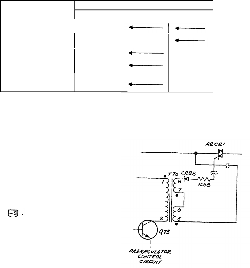
Manual Changes/Model 6269B
Manual HP Part No, 06269-90002
Page -2-
CHANGE 5:
The standard colors for this instrument are now
mint gray (for front and rear panels) and olive, gray
(for all top, bottom, side, and other external sur-
faces).
Option X95 designates use of the former
color scheme of light gray and blue gray. Option
A85 designates use of a light gray front panel with
olive gray used for all other external surfaces.
CHANGE 6:
In the Replaceable Parts list and on the schematic,
make the following changes:
A1R24: Change to 127k Ω, ±25%, 1/8W, HP Part
No. 0698-6659.
A1R25: Change to 90.9k Ω, ±1%, 1/8W, HP Part
No. 0757-0464.
These changes insure that the Short Circuit Protec-
New part numbers are shown below:
tion circuit operates correctly.
HP PART NO.
DESCRIPTION
STANDARD
OPTION A85 OPTION X95
Front Panel, Complete I06269-60005
Front Panel, Lettered
06269-60009
Rear Panel 5000-9475
Cover, Top and Bottom
5000-9476
Chassis, Assembly
(weIded) 5060-7972
06269-60006
5000-6247
5000-6250
5060-6186
CHANGE 7:
with the secondary winding of the new Pulse
Generator Pulse Transformer T70 (HP Part No.
In the replaceable parts table under AI Main P. C.
5080-7192) as shown below:
Board - Electrical and on the schematic (in the
Overvoltage Protection Crowbar circuit), make the
following changes:
C91: Add, 0.0047µF, 200V, HP Part No. 0160-
0157.
R99: Change to 10k Ω, ±5%, ½W, HP Part No.
0686-1035.
T70, T90: Change to HP Part No. 5080-7192.
The above changes have been made to improve the
noise immunity of the overvoltage protection crow-
bar and thereby eliminate spurious triggering of the
crowbar.
Capacitor C91 is connected from between
the collector of Q92 (which also connects to the
base of Q91) and
The top of R99 has been
disconnected fmm +12.4V and connected instead to
the junction of R94-R95 (the other end of R95 still
connects to the base of Q92 through CR91).
In order to eliminate false triggering and ripple im-
balance in the Preregulator Control Circuit, the
following changes have been made:
Diode CR88 and resistor R88 are now in series
CHANGE 8:
In the replaceable parts table under A2 RFI Filter
Assembly, change Triac CR1 HP Part No. to 1884-
0218.
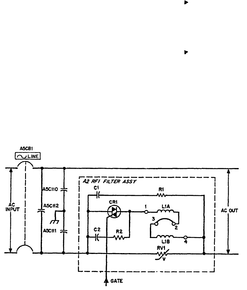
CHANGE 12:
Manual Changes/Model 6269B
Manual HP Part No. 04269-90002
Page -3-
ERRATA :
In the parts list
Under A4 Mechanical, add Transistor Insu-
lator, HP Part No. 0340-0795, quantity 2.
Under AS Front Panel Assembly, change the
HP Part No. of circuit breaker CB1 to
3105-0034.
CHANGE 9:
In the parts list under A4 Heat Sink Assembly,
change the HP Part No. of CR101, 102, 105, and
108 to 1901-0318, and change CR103, 104, and
106 to 1901-0317.
CHANGE 10:
In the parts list under AS Front Panel Assembly,
change R122 to 100 ohms, variable, HP Part No.
2100-1987.
CHANGE 11:
In the parts list and on the schematic, make the
following additions and changes:
Under AS: Add C112, fxd, .01µF 3KV HP Part
No. 0160-2568
Under A2: Add RV1, varistor, MOV HP Part No.
0837-0117
Change: C110 and C111 have been moved from
chassis to the front panel assembly. Connect
the added and changed components as shown
below.
The following changes enable the master crowbar
to trip the slave crowbar(s) when two or more
units are connected in parallel. In the parts list
under Al Main Printed Circuit Board and on the
schematic, change A1C90 to .47µF 25Vdc HP Part
No. 0160-0174. Also, add resistor A1R120, 4.7K
¼W HP Part No. 0758-0005. Connect A1R20 in
parallel with A1Z2C in the Overvoltage Protection
Crowbar Circuit on schematic.
The following change prevents series regulator
failure under short circuit conditions. On sche-
matic, in the Constant Voltage Comparator Cir-
cuit disconnect anode of A1CR6 from A1Z1 pin 1
side of A1R6. Connect anode of A1CR6 to rear
terminal A2 side of A1R6.
CHANGE 13:
In the parts list under A4 Heat Sink Assembly.
change the part number of CR101 and CR102 to
1901-0729 and change CR103 and CR104 to 1901-
0730.
CHANGE 14:
The RFI Assembly is changed to HP Part No. 06269-
60010. This new RFI Assembly is completely inter-
changeable in all previously built 6269B power
supplies.
In the parts list under A2-Mechanical make the
following changes:
Change the Cover, RFI Assembly to 5020-
2284.
Change the Heat Sink, RFI Filter Ass ‘y to
5020-2282.
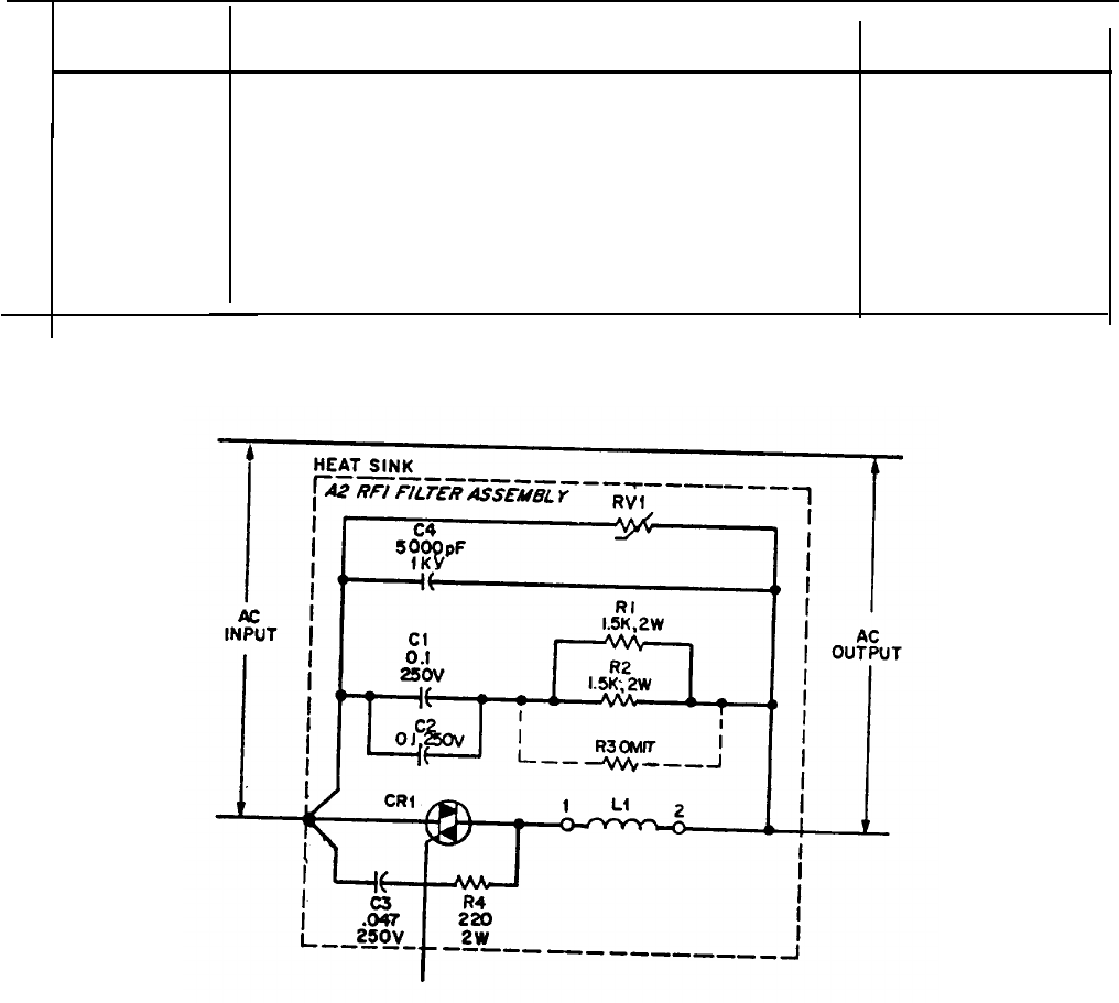
Manual Changes/Model 6269B
Manual HP Part No. 06269-90002
Page -4-
In the parts list, delete the entire listing under A schematic of RFI Filter Assembly 06269-60010
A2 RFI Filter Assembly and replace with the fol-
lowing. is shown below. This schematic replaces the A2
Filter portion of the schematic shown in Change 11.
REF.
HP
DESIG.
DESCRIPTON
PART NO.
A2
RFI Filter Assembly
C1, C2
06269-60010
fxd, metalized paper, 0.1µF 250Vac
C3
fxd, metalized paper, .047µF 250v
0160-4065
C4
0160-4323
fxd mica, 5000pF, 1kV
CR1
0160-0899
Thyristor, Si. (Triac)
L1
Filter choke, 20A
1884-0248
R1, R2
5080-1782
fxd, metal oxide, 1.5k Ω 2W
R4
0698-3338
fxd, metal oxide, 220 Ω 2W
RV1
Varistor, MOV
0698-3628
0837-0117
9-26-75

By Order of the Secretary of the Army:
Official:
J. C. PENNINGTON
Major General, United States Army
The Adjutant General
Distribution:
Active Army:
TSG (1)
USAERDAA (1)
USAARENBD (1) USAERDAW (1)
USAINSCOM (2) Army Dep (1) except
TRADOC (2) SAAD (20)
DARCOM (1) TOAD (14)
TECOM (2) SHAD (2)
OS Maj Cored (2) USA Dep (1)
USACC (2) Sig Sec USA Dep (1)
HISA (Ft Monmouth) (21) Units org under fol TOE:
Armies (1)
(2 copies each unit)
USASIGS (10)
29-207
Svc Colleges (1)
29-610
Ft Richardson (CERCOM Oft) (1)
(1 copy each unit)
Ft Carson (5)
29-134
Ft Gillem (10)
29-136
WSMR (1)
ARNG; None
USAR: None
For explanation of abbreviations used, see AR 310-50.
E. C. MEYER
General, United States Army
Chief of Staff
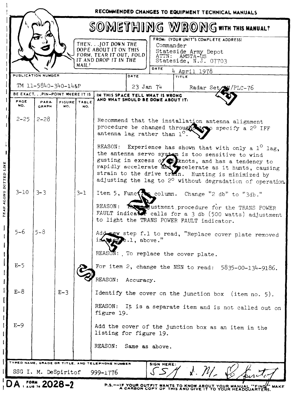
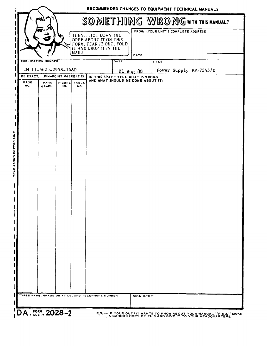
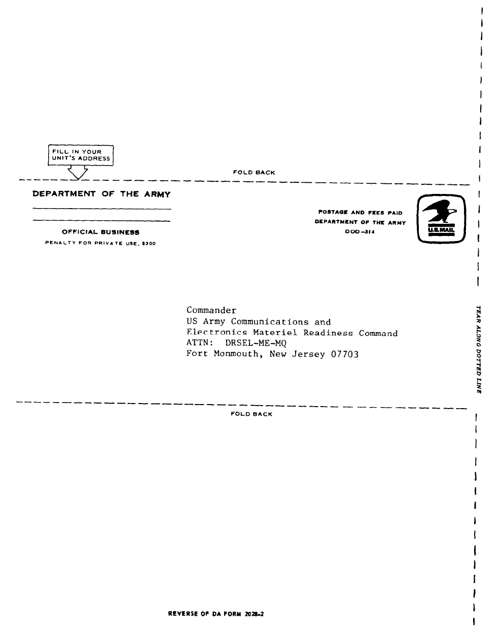
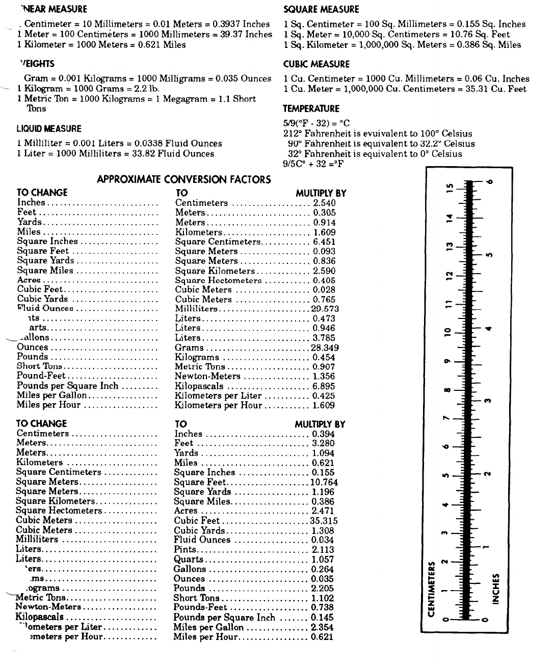
THE METRIC SYSTEM AND EQUIVALENTS

PIN: 046413-000