Huawei Technologies HIKEY970 Hikey970 User Manual
Huawei Technologies Co.,Ltd Hikey970
Contents
- 1. User Manual
- 2. User_Manual
User Manual

HiKey970
User Guide
Issue 01
Date 2018-03-11

Issue 01 (2018-03-11) HiSilicon Proprietary and Confidential
Copyright © HiSilicon Technologies Co., Ltd. i
Copyright © HiSilicon Technologies Co., Ltd. 2018. All rights reserved.
No part of this document may be reproduced or transmitted in any form or by any means without prior written
consent of HiSilicon Technologies Co., Ltd.
Trademarks and Permissions
, , and other HiSilicon icons are trademarks of HiSilicon Technologies Co., Ltd.
All other trademarks and trade names mentioned in this document are the property of their respective holders.
Notice
The purchased products, services and features are stipulated by the contract made between HiSilicon and the
customer. All or part of the products, services and features described in this document may not be within the
purchase scope or the usage scope. Unless otherwise specified in the contract, all statements, information,
and recommendations in this document are provided "AS IS" without warranties, guarantees or
representations of any kind, either express or implied.
The information in this document is subject to change without notice. Every effort has been made in the
preparation of this document to ensure accuracy of the contents, but all statements, information, and
recommendations in this document do not constitute a warranty of any kind, express or implied.
HiSilicon Technologies Co., Ltd.
Address: Huawei Industrial Base
Bantian, Longgang
Shenzhen 518129
People's Republic of China
Website: http://www.hisilicon.com
Email: support@hisilicon.com

HiKey970
User Guide Change History
Issue 01 (2018-03-11) HiSilicon Proprietary and Confidential
Copyright © HiSilicon Technologies Co., Ltd. i
Change History
Changes between document issues are cumulative. The latest document issue
contains all the changes made in earlier issues.
Issue 01 (2018-03-11)
The first version.

HiKey970
User Guide Contents
Issue 01 (2018-03-11) HiSilicon Proprietary and Confidential
Copyright © HiSilicon Technologies Co., Ltd. ii
Contents
Change History .................................................................................................................................. i
Contents ............................................................................................................................................ ii
User Guide ......................................................................................................................................... 1
1.1 Introduction ...................................................................................................................................................... 1
1.1.1 Board overview ....................................................................................................................................... 1
1.1.2 Key features ............................................................................................................................................ 4
1.2 Getting started .................................................................................................................................................. 5
1.2.1 Prerequisites ............................................................................................................................................ 5
1.2.2 Starting the board for the first time ......................................................................................................... 5
1.3 HiKey970 Overview ........................................................................................................................................ 5
1.3.1 Boot switches and UART debug ............................................................................................................. 5
1.3.2 POWER on button /reset button .............................................................................................................. 6
1.3.3 DC in jack ............................................................................................................................................... 7
1.3.4 Low speed expansion connector ............................................................................................................. 7
1.3.5 High speed expansion connector ............................................................................................................. 8
1.3.6 Antenna connector .................................................................................................................................. 9
1.3.7 Display interfaces .................................................................................................................................. 10
1.3.8 USB interfaces ...................................................................................................................................... 10
1.3.9 System and user LEDs .......................................................................................................................... 11
1.3.10 JTAG header ....................................................................................................................................... 11
1.3.11 Ethernet ............................................................................................................................................... 12
1.4 FCC Regulations: ........................................................................................................................................... 12
FCC RF Radiation Exposure Statement ..................................................................................... 12

HiKey970
User Guide 1 User Guide
Issue 01 (2018-03-11) HiSilicon Proprietary and Confidential
Copyright © HiSilicon Technologies Co., Ltd. 1
User Guide
1.1 Introduction
The HiKey970 board is a 96Boards compliant community board based on HiSilicon Kirin 970
series of SOC’s.
The following table lists its key features:
1.1.1 Board overview
Figure 1-1 Top side view of the HiKey PCB

HiKey970
User Guide 1 User Guide
Issue 01 (2018-03-11) HiSilicon Proprietary and Confidential
Copyright © HiSilicon Technologies Co., Ltd. 2
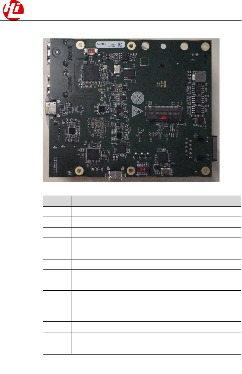
Figure 1-2 Bottom side view of the HiKey PCB
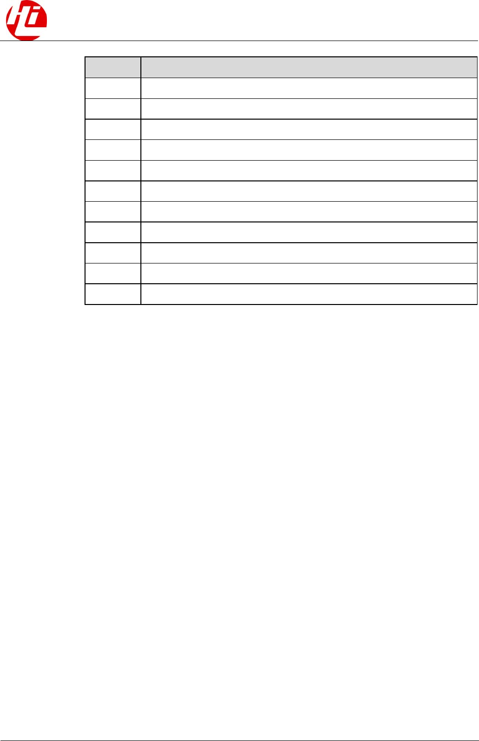
Number Description
01 (J2502)Micro SD Card Socket
02 (J2001)HDMI Type A Port
03 (J1801)USB Type C
04 (D3305)LED,(D3306)WIFI LED
05 (J1901)USB Type A
06 (D3301~D3304)User LED
07 (J1902) USB Type A
08 (J3101) UART Debug
09 (J2103) High Speed Expansion Connector
10 (U501) Kirin970 Processor
11 (U2203)WLAN
12 (D3307)CAN LED, (D3308)GPS LED
13 (J2301)GPS Antenna Connector
14 (U2201,U2202)WIFI Antenna

HiKey970
User Guide 1 User Guide
Issue 01 (2018-03-11) HiSilicon Proprietary and Confidential
Copyright © HiSilicon Technologies Co., Ltd. 3
Number Description
15 (J2101)Low Speed Expansion Connector
16 (S2403)Power Button
17 (S2402)Reset Button
18 (J3001) Ethernet Connector
19 (J2901)PCIE MINI Connector
20 (P401)Power Jack
21 (D404)Power LED’s
22 (SW2402)Boot Switches
23 (J3201)CAN Connector
24 (J2501)JATG Connector
25 (J2801)PCIE M.2 Connector

HiKey970
User Guide 1 User Guide
Issue 01 (2018-03-11) HiSilicon Proprietary and Confidential
Copyright © HiSilicon Technologies Co., Ltd. 4
1.1.2 Key features
Processor HiSilicon Kirin 970
ARM Cortex-A73 MPCore*4 @up to2.36GHz
ARM Cortex-A53 MPCore*4 @up to1.8GHz
ARM Mali-G72 MP12 GPU
HiAI Architecture
Dedicated NPU
Memory 6GB LPDDR4X 1866MHz
Storage 64GB UFS 2.1
Micro SD
Video 1080p@60Hz HDMI
4 line MIPI/LCD port
Camera Support 4 line MIPI port
2 line MIPI port
Connectivity WIFI(DFS band not support)
I/O Interfaces One 40-pin Low Speed (LS) expansion connector
• UART, SPI, I2S, I2C x2, GPIO x12, DC power
One 60-pin High Speed (HS) expansion connector
• 4L-MIPI DSI, USB, I2C x2, 2L+4L-MIPI CSI
User Interface Power/Reset
8 LED indicators
• 4 -user controllable
• 3 -for radios
• 1 – for CAN
OS-support Android
Linux
Power DC Power: +8V to +18V
Mechanical Dimensions: 105.26mm by 100mm meeting 96Boards™
Consumer Edition standard dimensions specifications.
Environmental Operating Temp: 0°C to +70°C
RoHS and Reach compliant
HiKey970
User Guide 1 User Guide
Issue 01 (2018-03-11) HiSilicon Proprietary and Confidential
Copyright © HiSilicon Technologies Co., Ltd. 5
1.2 Getting started
1.2.1 Prerequisites
Before you power up your HiKey970 board for the first time you will need the following:
HiKey970 board.
A 96Boards compliant power supply.
A HDMI LCD Monitor that supports a resolution of 1080P/60Hz.
HDMI-HDMI cable cable to connect the board to the Monitor.
A computer keyboard with USB interface
A computer mouse with USB interface.
1.2.2 Starting the board for the first time
To start the board, follow these simple steps:
Step 1. Connect the HDMI cable to the HiKey970 HDMI connector (marked J2001) and to
the LCD Monitor.
Step 2. Connect the keyboard to the boards USB connector marked J1901(or J1902) and the
mouse to the USB connector marked J1902(or J1901).
Step 3. Ensure that the boot switches SW2402 are set to ‘1000’, on/off/off/off position.
Step 4. Connect the power supply to power connector J401.
Once you plug the power supply into a power outlet the board will start the booting process,
and you should see Android boot up.
Please note that the first boot takes several minutes due to Androids initialization. Subsequent
boot times should be faster.
1.3 HiKey970 Overview
1.3.1 Boot switches and UART debug
The HiKey board has multiple boot options that are user selectable in hardware which can be
set via Switch SW2402.
Figure 1-3 Boot switches
HiKey970
User Guide 1 User Guide
Issue 01 (2018-03-11) HiSilicon Proprietary and Confidential
Copyright © HiSilicon Technologies Co., Ltd. 6
SW2402
1 AUTO_POWER
2 BOOT_MODE
3 EXT_BOOT
4 I2S_SEL
Auto Power Switch
ON: system will boot up automatically when the power supply is applied.
OFF : Pressing the power switch is required to boot up the system.
Boot Setting Switch
ON: the will attempt to program the UFS flash from USB OTG source. This should ONLY be
used if the first stage bootloader is corrupted or needs to be replaced.
OFF : the unit boots from the first stage bootloader installed in the onboard UFS device.
User Jumper
Connected to GPIO_055 on the SoC and UEFI mode
ON : GPIO_055 will be pulled low, the board will boot up UEFI mode
OFF: GPIO_055 will be pulled High, the board will boot up the system
I2S SEL
ON: I2S0 will connect Low Speed Expansion Connector
OFF: I2S0 will connect other channel.
The HiKey board also has an option for a Debug UART Type C J3101. This is normally used
by the first stage bootloader developers, and is connected to the UART6 port of the SoC.
1.3.2 POWER on button /reset button
The power button S2403 can be used to power up, power down the system.
A simple press and release powers ON the board provided the Auto Power Jumper is not
installed.
A press and release will then power OFF the board
The Reset button S2402 can be used to reset the system.
HiKey970
User Guide 1 User Guide
Issue 01 (2018-03-11) HiSilicon Proprietary and Confidential
Copyright © HiSilicon Technologies Co., Ltd. 7
Figure 1-4 Powr/Reset
It is also possible to connect external switches for power on/off . This is implemented by
routing the specific power signals to the low speed bus connector J2101.4(PWRON_N) and
J2401.6(EXP_RSTOUT_N).
1.3.3 DC in jack
DC Power is provided via the DC jack at P401. This is a CUI PJ-041H connector with a
center pin diameter of 1.65mm configured with positive polarity (center +). An 8V up to 18V
power supply at a minimum of 2A rating can be used to provide sufficient board power for on
system requirements as well as external devices. Additional current rating may be required for
mezzanine boards or modules. DC Power can also be supplied via the SYS_DCIN pins on the
low speed expansion J2101.
NOTE: Power should not be supplied simultaneously from multiple sources
1.3.4 Low speed expansion connector
The HiKey board features two expansion connectors: one low speed expansion connector and
one high speed. The low speed expansion connector carries GPIO and other low speed
interfaces. The connector is a low profile 40 pin female 2mm receptacle (20x2) of a specified
height of 4.5mm height.
The low speed expansion brings out 1.8V level SoC signals such as UART2 and UART3,
I2C0 and I2C1, GPIO signals as well as SPI, Audio, Reset, 1.8V and Ground. The complete
list of SoC signals is shown in Table 1 below:
96Boards Signals HiKey970 Signals Pin Pin HiKey970 Signals 96Boards Signals
GND GND 1 2
GND GND
UART0_CTS UART2_CTS_N 3 4
PWRON_N PWR_BTN_N
UART0_TxD UART2_RXD 5 6
EXP_RSTOUT_N RST_BTN_N
UART0_RxD UART2_RXD 7 8
SPI2_CLK SPI0_SCLK
UART0_RTS UART2_RTS_N 9 10
SPI2_DI SPI0_DIN
HiKey970
User Guide 1 User Guide
Issue 01 (2018-03-11) HiSilicon Proprietary and Confidential
Copyright © HiSilicon Technologies Co., Ltd. 8
96Boards Signals HiKey970 Signals Pin Pin HiKey970 Signals 96Boards Signals
UART1_TxD DEBUG_UART6_TX
D 11 12 SPI2_CS0_N SPI0_CS
UART1_RxD DEBUG_UART6_RX
D 13 14 SPI2_DO SPI0_DOUT
I2C0_SCL I2C0_SCL 15 16 EXT_I2S0_XFS PCM_FS
I2C0_SDA I2C0_SDA 17 18 EXT_I2S0_XCLK PCM_CLK
I2C1_SCL I2C2_SCL 19 20 EXT_I2S0_DO PCM_DO
I2C1_SDA I2C2_SDA 21 22 EXT_I2S0_DI PCM_DI
GPIO-A GPIO_208_WAKEU
P_SOC 23 24 GPIO_171 GPIO-B
GPIO-C GPIO_169 25 26 GPIO_052 GPIO-D
GPIO-E GPIO_170 27 28 LCD_BL_PWM GPIO-F
GPIO-G LCD_TE0 29 30 GPIO_029_LCD_RS
T_N GPIO-H
GPIO-I GPIO_013_CAM0_R
ST_N 31 32 GPIO_053 GPIO-J
GPIO-K GPIO_032_CAM1_R
ST_N 33 34 GPIO_031 GPIO-L
+1V8 VOUT4_1V8 35 36 SYSDC_IN SYS_DCIN
+5V SYS_5V 37 38 SYSDC_IN SYC_DCIN
GND GND 39 40 GND GND
The HiKey board can also drive 5V or 12V cooling fans. The power for these is available on
the low speed Expansion connector and can be supplied through a 2-pin 2mm male header
inserted at pins J2101.37-J2101.39 or J2101.38-J2101.40, respectively
1.3.5 High speed expansion connector
The HS Expansion connector is a board to board low profile 60 pin receptacle TE part.
96Boards Signals HiKey970 Signals Pin Pin HiKey970 Signals 96Boards
Signals
SD_DAT0/SPI1_DOUT SPI3_DO 1 2 CSI0_CLK_P CSI0_C+
SD_DAT1 UART0_RXD 3 4 CSI0_CLK_N CSI0_C-
SD_DAT2 UART0_TXD 5 6 GND GND
SD_DAT3/SPI1_CS SPI3_CS0_N 7 8 CSI0_DATA0_P CSI0_D0+
SD_SCLK/SPI1_SCLK SPI3_CLK 9 10 CSI0_DATA0_N CSI0_D0-

HiKey970
User Guide 1 User Guide
Issue 01 (2018-03-11) HiSilicon Proprietary and Confidential
Copyright © HiSilicon Technologies Co., Ltd. 9
96Boards Signals HiKey970 Signals Pin Pin HiKey970 Signals 96Boards
Signals
SD_CMD/SPI1_DIN SPI3_DI 11 12 GND GND
GND GND 13 14 CSI0_DATA1_P CSI0_D1+
CLK0/CSI0_MCLK ISP_CCLK0_MCAM 15 16 CSI0_DATA1_N CSI0_D1-
CLK1/CSI1_MCLK ISP_CCLK1_SCAM 17 18 GND GND
GND GND 19 20 CSI0_DATA2_P CSI0_D2+
DSI_CLK+ DSI2_CLK_P 21 22 CSI0_DATA2_N CSI0_D2-
DSI_CLK- DSI2_CLK_N 23 24 GND GND
GND GND 25 26 CSI0_DATA3_P CSI0_D3+
DSI_D0+ DSI2_DATA0_P 27 28 CSI0_DATA3_N CSI0_D3-
DSI_D0- DSI2_DATA0_N 29 30 GND GND
GND GND 31 32 ISP_SCL0 I2C2_SCL
DSI_D1+ DSI2_DATA1_P 33 34 ISP_SDA0 I2C2_SDA
DSI_D1- DSI2_DATA1_N 35 36 ISP_SCL1 I2C3_SCLL
GND GND 37 38 ISP_SDA1 I2C3_SDA
DSI_D2+ DSI2_DATA2_P 39 40 GND GND
DSI_D2- DSI2_DATA2_N 41 42 CSI1_DATA0_P CSI1_D0+
GND GND 43 44 CSI1_DATA0_N CSI1_D0-
DSI_D3+ DSI3_DATA3_P 45 46 GND GND
DSI_D3- DSI3_DATA3_N 47 48 CSI1_DATA1_P CSI1_D1+
GND GND 49 50 CSI1_DATA1_N CSI1_D1-
USB_D+ USB_DP_HUB_DN4
_CON 51 52 GND GND
USB_D- USB_DM_HUB_DN
4_CON 53 54 CSI1_CLK_P CSI1_C+
GND GND 55 56 CSI1_CLK_N CSI1_C-
HSIC_STR NA 57 58 GND GND
HSIC_DATA NA 59 60 VOUT4_1V8 RESERVED
1.3.6 Antenna connector
The HiKey board is equipped with a TI WL1835MOD WLAN Baseband Processor and RF
Transceiver which supports IEEE 802.11a, 802.11b, 802.11g and 802.11n WiFi.

HiKey970
User Guide 1 User Guide
Issue 01 (2018-03-11) HiSilicon Proprietary and Confidential
Copyright © HiSilicon Technologies Co., Ltd. 10
A PCB chip antenna is available onboard by default but also an external antenna socket option
is provided via J201&J2202 footprint. A Hirose U.FL-R-SMT connector can be soldered at
J2201&J2202 location.
The HiKey board is equipped with a Broadcom BCM4753 GPS Baseband Processor and RF
Transceiver. A Hirose U.FL-R-SMT connector can be soldered at J2301 location.
1.3.7 Display interfaces
The on board HDMI is provided via the Analog Devices ADV7535 multifunction video
interface chip is available on the Type A HDMI connector mounted at J2001. This connector
is ESD protected with TI protection diodes.
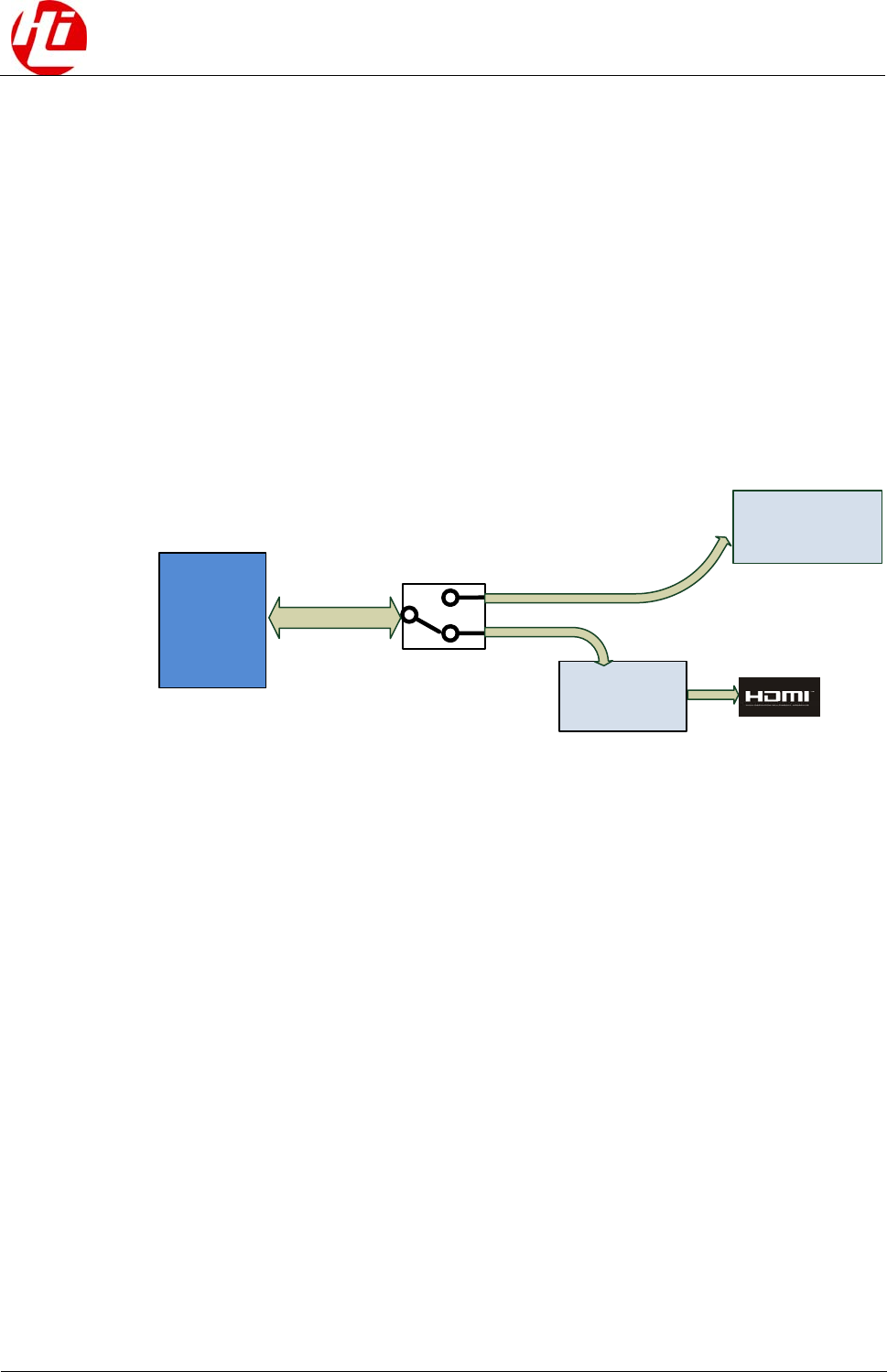
A 4 lane MIPI/DSI port is provided on the HS Expansion bus interface. Below is a block
diagram of the HiKey implementation.
Figure 1-5 HDMI&LCD
Hi3670
DSI-HDMI
ADV7535
HS IO EXP
J2103
DSI0
SWITCH
J2001
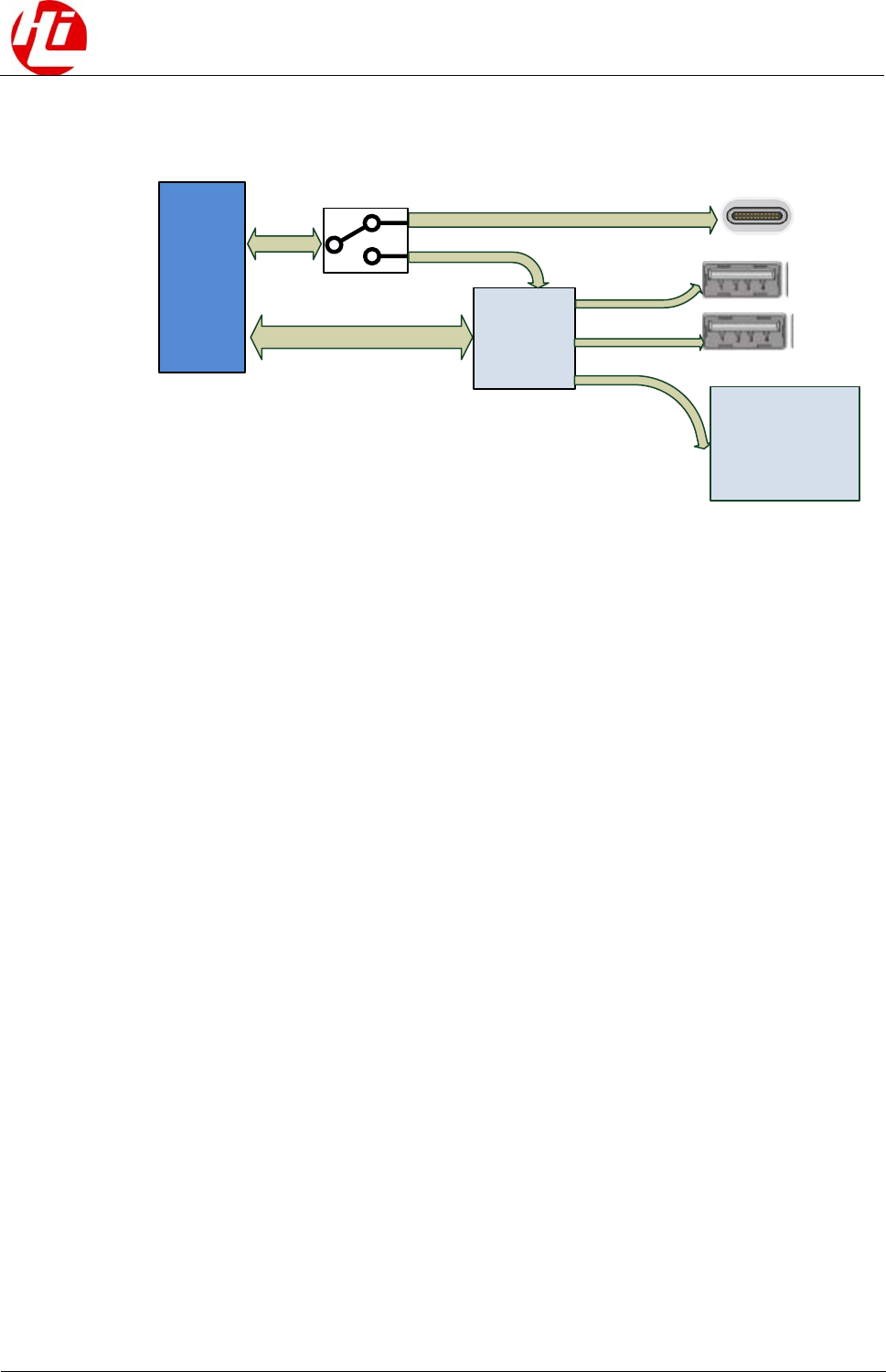
1.3.8 USB interfaces
There are a total of 4 USB ports on the HiKey board. Two Type-A USB 3.0 host ports at
J1901 and J1902, one type C 2.0 host/slave port at P1801 and one USB host port available on
the High Speed Expansion bus.
HiKey970
User Guide 1 User Guide
Issue 01 (2018-03-11) HiSilicon Proprietary and Confidential
Copyright © HiSilicon Technologies Co., Ltd. 11
Figure 1-6 USB
USB
USB3.0
HUB
USB5734
USB
TYPE C
USB 3.0 TX/RX
USB 2.0
DP/DM
SWITCH
HS IO EXP
J2103
USB
TYPE A
GPIO_034_USBSW_SEL
The HiKey board utilizes a single SoC USB interface without USB protocol hardware split
transfer support. The USB interfaces are therefore subject to the following restrictions:
The type C or the Type A/Mezzanine board interfaces may be used depending on the
state of GPIO_034_USBSW_SEL. Both interfaces may not be used at the same time.
The type C port supports a single attached device with USB slave operations or USB
host high speed, full speed or low speed operations.
The Type A/Mezzanine board interfaces cannot support mixed speed devices. All
attached devices must be of the same type – high speed, full speed or low speed.
Furthermore, the HiKey board must be configured in software to support either full
speed/low speed devices (default) or high/super speed devices on these ports.
1.3.9 System and user LEDs
There are four status LEDs and four User LEDs on the HiKey board. The user LEDs can be
programmed by the SoC directly.
D3305 – WiFi LED
The WiFi activity LED is a Yellow type surface mount 0603 LED.
D3306- LED
The activity LED is a Blue Type surface mount 0603 LED .
D3301-D3304 – USER LEDs
The four user LEDs are surface mount Green Type 0603 LED .
D3308-GPS LED
D3307-CAN LED
1.3.10 JTAG header
The HiKey board includes the option for soldering a 10 pin header that brings out the SoC
signals for JTAG debug. A FTSH-105-01-F-DV header can be populated at J2501.

HiKey970
User Guide 1 User Guide
Issue 01 (2018-03-11) HiSilicon Proprietary and Confidential
Copyright © HiSilicon Technologies Co., Ltd. 12
1.3.11 Ethernet
Hikey970 board reserved an Ethernet connector, but Ethernet function is not supported by
current software.
1.4 FCC Regulations:
This device complies with part 15 of the FCC Rules. Operation is subject to the following two
conditions: (1) This device may not cause harmful interference, and (2) this device must accept
any interference received, including interference that may cause undesired operation.
This equipment has been tested and found to comply with the limits for a Class B digital device,
pursuant to part 15 of the FCC Rules. These limits are designed to provide reasonable
protection against harmful interference in a residential installation. This equipment generates,
uses and can radiate radio frequency energy and, if not installed and used in accordance with
the instructions, may cause harmful interference to radio communications. However, there is no
guarantee that interference will not occur in a particular installation. If this equipment does
cause harmful interference to radio or television reception, which can be determined by turning
the equipment off and on, the user is encouraged to try to correct the interference by one or
more of the following measures:
—Reorient or relocate the receiving antenna.
—Increase the separation between the equipment and receiver.
—Connect the equipment into an outlet on a circuit different from that to which the receiver is
connected.
—Consult the dealer or an experienced radio/ TV technician for help.
Changes or modifications not expressly approved by the manufacturer could void the user’s
authority to operate the equipment.
FCC RF Radiation Exposure Statement

HiKey970
User Guide 1 User Guide
Issue 01 (2018-03-11) HiSilicon Proprietary and Confidential
Copyright © HiSilicon Technologies Co., Ltd. 13
This equipment complies with FCC radiation exposure limits set forth for an uncontrolled
environment. To comply with FCC RF Exposure compliance requirements, this grant is applicable
to only Mobile Configurations. The antennas used for the transmitter must be installed to provide a
separation distance of at least 20cm from all persons and must not be co-located or operating in
conjunction with any other antenna or transmitter.
User_Manual

HiKey970
User Guide
Issue 01
Date 2018-03-11

Issue 01 (2018-03-11) HiSilicon Proprietary and Confidential
Copyright © HiSilicon Technologies Co., Ltd. i
Copyright © HiSilicon Technologies Co., Ltd. 2018. All rights reserved.
No part of this document may be reproduced or transmitted in any form or by any means without prior written
consent of HiSilicon Technologies Co., Ltd.
Trademarks and Permissions
, , and other HiSilicon icons are trademarks of HiSilicon Technologies Co., Ltd.
All other trademarks and trade names mentioned in this document are the property of their respective holders.
Notice
The purchased products, services and features are stipulated by the contract made between HiSilicon and the
customer. All or part of the products, services and features described in this document may not be within the
purchase scope or the usage scope. Unless otherwise specified in the contract, all statements, information,
and recommendations in this document are provided "AS IS" without warranties, guarantees or
representations of any kind, either express or implied.
The information in this document is subject to change without notice. Every effort has been made in the
preparation of this document to ensure accuracy of the contents, but all statements, information, and
recommendations in this document do not constitute a warranty of any kind, express or implied.
HiSilicon Technologies Co., Ltd.
Address: Huawei Industrial Base
Bantian, Longgang
Shenzhen 518129
People's Republic of China
Website: http://www.hisilicon.com
Email: support@hisilicon.com

HiKey970
User Guide Change History
Issue 01 (2018-03-11) HiSilicon Proprietary and Confidential
Copyright © HiSilicon Technologies Co., Ltd. i
Change History
Changes between document issues are cumulative. The latest document issue
contains all the changes made in earlier issues.
Issue 01 (2018-03-11)
The first version.

HiKey970
User Guide Contents
Issue 01 (2018-03-11) HiSilicon Proprietary and Confidential
Copyright © HiSilicon Technologies Co., Ltd. ii
Contents
Change History .................................................................................................................................. i
Contents ............................................................................................................................................ ii
User Guide ......................................................................................................................................... 1
1.1 Introduction ...................................................................................................................................................... 1
1.1.1 Board overview ....................................................................................................................................... 1
1.1.2 Key features ............................................................................................................................................ 4
1.2 Getting started .................................................................................................................................................. 5
1.2.1 Prerequisites ............................................................................................................................................ 5
1.2.2 Starting the board for the first time ......................................................................................................... 5
1.3 HiKey970 Overview ........................................................................................................................................ 5
1.3.1 Boot switches and UART debug ............................................................................................................. 5
1.3.2 POWER on button /reset button .............................................................................................................. 6
1.3.3 DC in jack ............................................................................................................................................... 7
1.3.4 Low speed expansion connector ............................................................................................................. 7
1.3.5 High speed expansion connector ............................................................................................................. 8
1.3.6 Antenna connector .................................................................................................................................. 9
1.3.7 Display interfaces .................................................................................................................................. 10
1.3.8 USB interfaces ...................................................................................................................................... 10
1.3.9 System and user LEDs .......................................................................................................................... 11
1.3.10 JTAG header ....................................................................................................................................... 11
1.3.11 Ethernet ............................................................................................................................................... 12
1.4 FCC Regulations: ........................................................................................................................................... 12
FCC RF Radiation Exposure Statement ..................................................................................... 12
HiKey970
User Guide 1 User Guide
Issue 01 (2018-03-11) HiSilicon Proprietary and Confidential
Copyright © HiSilicon Technologies Co., Ltd. 1
User Guide
1.1 Introduction
The HiKey970 board is a 96Boards compliant community board based on HiSilicon Kirin 970
series of SOC’s.
The following table lists its key features:
1.1.1 Board overview
Figure 1-1 Top side view of the HiKey PCB
HiKey970
User Guide 1 User Guide
Issue 01 (2018-03-11) HiSilicon Proprietary and Confidential
Copyright © HiSilicon Technologies Co., Ltd. 2
Figure 1-2 Bottom side view of the HiKey PCB
Number Description
01 (J2502)Micro SD Card Socket
02 (J2001)HDMI Type A Port
03 (J1801)USB Type C
04 (D3305)LED,(D3306)WIFI LED
05 (J1901)USB Type A
06 (D3301~D3304)User LED
07 (J1902) USB Type A
08 (J3101) UART Debug
09 (J2103) High Speed Expansion Connector
10 (U501) Kirin970 Processor
11 (U2203)WLAN
12 (D3307)CAN LED, (D3308)GPS LED
13 (J2301)GPS Antenna Connector
14 (U2201,U2202)WIFI Antenna
HiKey970
User Guide 1 User Guide
Issue 01 (2018-03-11) HiSilicon Proprietary and Confidential
Copyright © HiSilicon Technologies Co., Ltd. 3
Number Description
15 (J2101)Low Speed Expansion Connector
16 (S2403)Power Button
17 (S2402)Reset Button
18 (J3001) Ethernet Connector
19 (J2901)PCIE MINI Connector
20 (P401)Power Jack
21 (D404)Power LED’s
22 (SW2402)Boot Switches
23 (J3201)CAN Connector
24 (J2501)JATG Connector
25 (J2801)PCIE M.2 Connector
HiKey970
User Guide 1 User Guide
Issue 01 (2018-03-11) HiSilicon Proprietary and Confidential
Copyright © HiSilicon Technologies Co., Ltd. 4
1.1.2 Key features
Processor HiSilicon Kirin 970
ARM Cortex-A73 MPCore*4 @up to2.36GHz
ARM Cortex-A53 MPCore*4 @up to1.8GHz
ARM Mali-G72 MP12 GPU
HiAI Architecture
Dedicated NPU
Memory 6GB LPDDR4X 1866MHz
Storage 64GB UFS 2.1
Micro SD
Video 1080p@60Hz HDMI
4 line MIPI/LCD port
Camera Support 4 line MIPI port
2 line MIPI port
Connectivity WIFI(DFS band not support)
I/O Interfaces One 40-pin Low Speed (LS) expansion connector
• UART, SPI, I2S, I2C x2, GPIO x12, DC power
One 60-pin High Speed (HS) expansion connector
• 4L-MIPI DSI, USB, I2C x2, 2L+4L-MIPI CSI
User Interface Power/Reset
8 LED indicators
• 4 -user controllable
• 3 -for radios
• 1 – for CAN
OS-support Android
Linux
Power DC Power: +8V to +18V
Mechanical Dimensions: 105.26mm by 100mm meeting 96Boards™
Consumer Edition standard dimensions specifications.
Environmental Operating Temp: 0°C to +70°C
RoHS and Reach compliant

HiKey970
User Guide 1 User Guide
Issue 01 (2018-03-11) HiSilicon Proprietary and Confidential
Copyright © HiSilicon Technologies Co., Ltd. 5
1.2 Getting started
1.2.1 Prerequisites
Before you power up your HiKey970 board for the first time you will need the following:
HiKey970 board.
A 96Boards compliant power supply.
A HDMI LCD Monitor that supports a resolution of 1080P/60Hz.
HDMI-HDMI cable cable to connect the board to the Monitor.
A computer keyboard with USB interface
A computer mouse with USB interface.
1.2.2 Starting the board for the first time
To start the board, follow these simple steps:
Step 1. Connect the HDMI cable to the HiKey970 HDMI connector (marked J2001) and to
the LCD Monitor.
Step 2. Connect the keyboard to the boards USB connector marked J1901(or J1902) and the
mouse to the USB connector marked J1902(or J1901).
Step 3. Ensure that the boot switches SW2402 are set to ‘1000’, on/off/off/off position.
Step 4. Connect the power supply to power connector J401.
Once you plug the power supply into a power outlet the board will start the booting process,
and you should see Android boot up.
Please note that the first boot takes several minutes due to Androids initialization. Subsequent
boot times should be faster.
1.3 HiKey970 Overview
1.3.1 Boot switches and UART debug
The HiKey board has multiple boot options that are user selectable in hardware which can be
set via Switch SW2402.
Figure 1-3 Boot switches

HiKey970
User Guide 1 User Guide
Issue 01 (2018-03-11) HiSilicon Proprietary and Confidential
Copyright © HiSilicon Technologies Co., Ltd. 6
SW2402
1 AUTO_POWER
2 BOOT_MODE
3 EXT_BOOT
4 I2S_SEL
Auto Power Switch
ON: system will boot up automatically when the power supply is applied.
OFF : Pressing the power switch is required to boot up the system.
Boot Setting Switch
ON: the will attempt to program the UFS flash from USB OTG source. This should ONLY be
used if the first stage bootloader is corrupted or needs to be replaced.
OFF : the unit boots from the first stage bootloader installed in the onboard UFS device.
User Jumper
Connected to GPIO_055 on the SoC and UEFI mode
ON : GPIO_055 will be pulled low, the board will boot up UEFI mode
OFF: GPIO_055 will be pulled High, the board will boot up the system
I2S SEL
ON: I2S0 will connect Low Speed Expansion Connector
OFF: I2S0 will connect other channel.
The HiKey board also has an option for a Debug UART Type C J3101. This is normally used
by the first stage bootloader developers, and is connected to the UART6 port of the SoC.
1.3.2 POWER on button /reset button
The power button S2403 can be used to power up, power down the system.
A simple press and release powers ON the board provided the Auto Power Jumper is not
installed.
A press and release will then power OFF the board
The Reset button S2402 can be used to reset the system.

HiKey970
User Guide 1 User Guide
Issue 01 (2018-03-11) HiSilicon Proprietary and Confidential
Copyright © HiSilicon Technologies Co., Ltd. 7
Figure 1-4 Powr/Reset
It is also possible to connect external switches for power on/off . This is implemented by
routing the specific power signals to the low speed bus connector J2101.4(PWRON_N) and
J2401.6(EXP_RSTOUT_N).
1.3.3 DC in jack
DC Power is provided via the DC jack at P401. This is a CUI PJ-041H connector with a
center pin diameter of 1.65mm configured with positive polarity (center +). An 8V up to 18V
power supply at a minimum of 2A rating can be used to provide sufficient board power for on
system requirements as well as external devices. Additional current rating may be required for
mezzanine boards or modules. DC Power can also be supplied via the SYS_DCIN pins on the
low speed expansion J2101.
NOTE: Power should not be supplied simultaneously from multiple sources
1.3.4 Low speed expansion connector
The HiKey board features two expansion connectors: one low speed expansion connector and
one high speed. The low speed expansion connector carries GPIO and other low speed
interfaces. The connector is a low profile 40 pin female 2mm receptacle (20x2) of a specified
height of 4.5mm height.
The low speed expansion brings out 1.8V level SoC signals such as UART2 and UART3,
I2C0 and I2C1, GPIO signals as well as SPI, Audio, Reset, 1.8V and Ground. The complete
list of SoC signals is shown in Table 1 below:
96Boards Signals HiKey970 Signals Pin Pin HiKey970 Signals 96Boards Signals
GND GND 1 2
GND GND
UART0_CTS UART2_CTS_N 3 4
PWRON_N PWR_BTN_N
UART0_TxD UART2_RXD 5 6
EXP_RSTOUT_N RST_BTN_N
UART0_RxD UART2_RXD 7 8
SPI2_CLK SPI0_SCLK
UART0_RTS UART2_RTS_N 9 10
SPI2_DI SPI0_DIN

HiKey970
User Guide 1 User Guide
Issue 01 (2018-03-11) HiSilicon Proprietary and Confidential
Copyright © HiSilicon Technologies Co., Ltd. 8
96Boards Signals HiKey970 Signals Pin Pin HiKey970 Signals 96Boards Signals
UART1_TxD DEBUG_UART6_TX
D 11 12 SPI2_CS0_N SPI0_CS
UART1_RxD DEBUG_UART6_RX
D 13 14 SPI2_DO SPI0_DOUT
I2C0_SCL I2C0_SCL 15 16 EXT_I2S0_XFS PCM_FS
I2C0_SDA I2C0_SDA 17 18 EXT_I2S0_XCLK PCM_CLK
I2C1_SCL I2C2_SCL 19 20 EXT_I2S0_DO PCM_DO
I2C1_SDA I2C2_SDA 21 22 EXT_I2S0_DI PCM_DI
GPIO-A GPIO_208_WAKEU
P_SOC 23 24 GPIO_171 GPIO-B
GPIO-C GPIO_169 25 26 GPIO_052 GPIO-D
GPIO-E GPIO_170 27 28 LCD_BL_PWM GPIO-F
GPIO-G LCD_TE0 29 30 GPIO_029_LCD_RS
T_N GPIO-H
GPIO-I GPIO_013_CAM0_R
ST_N 31 32 GPIO_053 GPIO-J
GPIO-K GPIO_032_CAM1_R
ST_N 33 34 GPIO_031 GPIO-L
+1V8 VOUT4_1V8 35 36 SYSDC_IN SYS_DCIN
+5V SYS_5V 37 38 SYSDC_IN SYC_DCIN
GND GND 39 40 GND GND
The HiKey board can also drive 5V or 12V cooling fans. The power for these is available on
the low speed Expansion connector and can be supplied through a 2-pin 2mm male header
inserted at pins J2101.37-J2101.39 or J2101.38-J2101.40, respectively
1.3.5 High speed expansion connector
The HS Expansion connector is a board to board low profile 60 pin receptacle TE part.
96Boards Signals HiKey970 Signals Pin Pin HiKey970 Signals 96Boards
Signals
SD_DAT0/SPI1_DOUT SPI3_DO 1 2 CSI0_CLK_P CSI0_C+
SD_DAT1 UART0_RXD 3 4 CSI0_CLK_N CSI0_C-
SD_DAT2 UART0_TXD 5 6 GND GND
SD_DAT3/SPI1_CS SPI3_CS0_N 7 8 CSI0_DATA0_P CSI0_D0+
SD_SCLK/SPI1_SCLK SPI3_CLK 9 10 CSI0_DATA0_N CSI0_D0-
HiKey970
User Guide 1 User Guide
Issue 01 (2018-03-11) HiSilicon Proprietary and Confidential
Copyright © HiSilicon Technologies Co., Ltd. 9
96Boards Signals HiKey970 Signals Pin Pin HiKey970 Signals 96Boards
Signals
SD_CMD/SPI1_DIN SPI3_DI 11 12 GND GND
GND GND 13 14 CSI0_DATA1_P CSI0_D1+
CLK0/CSI0_MCLK ISP_CCLK0_MCAM 15 16 CSI0_DATA1_N CSI0_D1-
CLK1/CSI1_MCLK ISP_CCLK1_SCAM 17 18 GND GND
GND GND 19 20 CSI0_DATA2_P CSI0_D2+
DSI_CLK+ DSI2_CLK_P 21 22 CSI0_DATA2_N CSI0_D2-
DSI_CLK- DSI2_CLK_N 23 24 GND GND
GND GND 25 26 CSI0_DATA3_P CSI0_D3+
DSI_D0+ DSI2_DATA0_P 27 28 CSI0_DATA3_N CSI0_D3-
DSI_D0- DSI2_DATA0_N 29 30 GND GND
GND GND 31 32 ISP_SCL0 I2C2_SCL
DSI_D1+ DSI2_DATA1_P 33 34 ISP_SDA0 I2C2_SDA
DSI_D1- DSI2_DATA1_N 35 36 ISP_SCL1 I2C3_SCLL
GND GND 37 38 ISP_SDA1 I2C3_SDA
DSI_D2+ DSI2_DATA2_P 39 40 GND GND
DSI_D2- DSI2_DATA2_N 41 42 CSI1_DATA0_P CSI1_D0+
GND GND 43 44 CSI1_DATA0_N CSI1_D0-
DSI_D3+ DSI3_DATA3_P 45 46 GND GND
DSI_D3- DSI3_DATA3_N 47 48 CSI1_DATA1_P CSI1_D1+
GND GND 49 50 CSI1_DATA1_N CSI1_D1-
USB_D+ USB_DP_HUB_DN4
_CON 51 52 GND GND
USB_D- USB_DM_HUB_DN
4_CON 53 54 CSI1_CLK_P CSI1_C+
GND GND 55 56 CSI1_CLK_N CSI1_C-
HSIC_STR NA 57 58 GND GND
HSIC_DATA NA 59 60 VOUT4_1V8 RESERVED
1.3.6 Antenna connector
The HiKey board is equipped with a TI WL1835MOD WLAN Baseband Processor and RF
Transceiver which supports IEEE 802.11a, 802.11b, 802.11g and 802.11n WiFi.
HiKey970
User Guide 1 User Guide
Issue 01 (2018-03-11) HiSilicon Proprietary and Confidential
Copyright © HiSilicon Technologies Co., Ltd. 10
A PCB chip antenna is available onboard by default but also an external antenna socket option
is provided via J201&J2202 footprint. A Hirose U.FL-R-SMT connector can be soldered at
J2201&J2202 location.
The HiKey board is equipped with a Broadcom BCM4753 GPS Baseband Processor and RF
Transceiver. A Hirose U.FL-R-SMT connector can be soldered at J2301 location.
1.3.7 Display interfaces
The on board HDMI is provided via the Analog Devices ADV7535 multifunction video
interface chip is available on the Type A HDMI connector mounted at J2001. This connector
is ESD protected with TI protection diodes.
A 4 lane MIPI/DSI port is provided on the HS Expansion bus interface. Below is a block
diagram of the HiKey implementation.
Figure 1-5 HDMI&LCD
Hi3670
DSI-HDMI
ADV7535
HS IO EXP
J2103
DSI0
SWITCH
J2001
1.3.8 USB interfaces
There are a total of 4 USB ports on the HiKey board. Two Type-A USB 3.0 host ports at
J1901 and J1902, one type C 2.0 host/slave port at P1801 and one USB host port available on
the High Speed Expansion bus.

HiKey970
User Guide 1 User Guide
Issue 01 (2018-03-11) HiSilicon Proprietary and Confidential
Copyright © HiSilicon Technologies Co., Ltd. 11
Figure 1-6 USB
USB
USB3.0
HUB
USB5734
USB
TYPE C
USB 3.0 TX/RX
USB 2.0
DP/DM
SWITCH
HS IO EXP
J2103
USB
TYPE A
GPIO_034_USBSW_SEL
The HiKey board utilizes a single SoC USB interface without USB protocol hardware split
transfer support. The USB interfaces are therefore subject to the following restrictions:
The type C or the Type A/Mezzanine board interfaces may be used depending on the
state of GPIO_034_USBSW_SEL. Both interfaces may not be used at the same time.
The type C port supports a single attached device with USB slave operations or USB
host high speed, full speed or low speed operations.
The Type A/Mezzanine board interfaces cannot support mixed speed devices. All
attached devices must be of the same type – high speed, full speed or low speed.
Furthermore, the HiKey board must be configured in software to support either full
speed/low speed devices (default) or high/super speed devices on these ports.
1.3.9 System and user LEDs
There are four status LEDs and four User LEDs on the HiKey board. The user LEDs can be
programmed by the SoC directly.
D3305 – WiFi LED
The WiFi activity LED is a Yellow type surface mount 0603 LED.
D3306- LED
The activity LED is a Blue Type surface mount 0603 LED .
D3301-D3304 – USER LEDs
The four user LEDs are surface mount Green Type 0603 LED .
D3308-GPS LED
D3307-CAN LED
1.3.10 JTAG header
The HiKey board includes the option for soldering a 10 pin header that brings out the SoC
signals for JTAG debug. A FTSH-105-01-F-DV header can be populated at J2501.

HiKey970
User Guide 1 User Guide
Issue 01 (2018-03-11) HiSilicon Proprietary and Confidential
Copyright © HiSilicon Technologies Co., Ltd. 12
1.3.11 Ethernet
Hikey970 board reserved an Ethernet connector, but Ethernet function is not supported by
current software.
1.4 FCC Regulations:
This device complies with part 15 of the FCC Rules. Operation is subject to the following two
conditions: (1) This device may not cause harmful interference, and (2) this device must accept
any interference received, including interference that may cause undesired operation.
This equipment has been tested and found to comply with the limits for a Class B digital device,
pursuant to part 15 of the FCC Rules. These limits are designed to provide reasonable
protection against harmful interference in a residential installation. This equipment generates,
uses and can radiate radio frequency energy and, if not installed and used in accordance with
the instructions, may cause harmful interference to radio communications. However, there is no
guarantee that interference will not occur in a particular installation. If this equipment does
cause harmful interference to radio or television reception, which can be determined by turning
the equipment off and on, the user is encouraged to try to correct the interference by one or
more of the following measures:
—Reorient or relocate the receiving antenna.
—Increase the separation between the equipment and receiver.
—Connect the equipment into an outlet on a circuit different from that to which the receiver is
connected.
—Consult the dealer or an experienced radio/ TV technician for help.
Changes or modifications not expressly approved by the manufacturer could void the user’s
authority to operate the equipment.
FCC RF Radiation Exposure Statement

HiKey970
User Guide 1 User Guide
Issue 01 (2018-03-11) HiSilicon Proprietary and Confidential
Copyright © HiSilicon Technologies Co., Ltd. 13
This equipment complies with FCC radiation exposure limits set forth for an uncontrolled
environment. To comply with FCC RF Exposure compliance requirements, this grant is applicable
to only Mobile Configurations. The antennas used for the transmitter must be installed to provide a
separation distance of at least 20cm from all persons and must not be co-located or operating in
conjunction with any other antenna or transmitter.