Huawei Technologies ME909U-523 LTE Module User Manual English
Huawei Technologies Co.,Ltd LTE Module English
Contents
- 1. InstallationInstructions.pdf
- 2. Safety Information.pdf
- 3. UserManual.pdf
InstallationInstructions.pdf

Copyright © Huawei Technologies Co., Ltd. 2014.
All rights reserved.
No part of this document may be reproduced or transmitted in any form or by any means without
prior written consent of Huawei Technologies Co., Ltd.
The product described in this manual may include copyrighted software of Huawei Technologies Co.,
Ltd and possible licensors. Customers shall not in any manner reproduce, distribute, modify,
decompile, disassemble, decrypt, extract, reverse engineer, lease, assign, or sublicense the said
software, unless such restrictions are prohibited by applicable laws or such actions are approved by
respective copyright holders under licenses.
Trademarks and Permissions
, , and are trademarks or registered trademarks of Huawei Technologies
Co., Ltd.
Other trademarks, product, service and company names mentioned are the property of their
respective owners.
Notice
Some features of the product and its accessories described herein rely on the software installed,
capacities and settings of local network, and may not be activated or may be limited by local
network operators or network service providers, thus the descriptions herein may not exactly match
the product or its accessories you purchase.
Huawei Technologies Co., Ltd reserves the right to change or modify any information or
specifications contained in this manual without prior notice or obligation.
NO WARRANTY
THE CONTENTS OF THIS MANUAL ARE PROVIDED “AS IS”. EXCEPT AS REQUIRED BY APPLICABLE
LAWS, NO WARRANTIES OF ANY KIND, EITHER EXPRESS OR IMPLIED, INCLUDING BUT NOT
LIMITED TO, THE IMPLIED WARRANTIES OF MERCHANTABILITY AND FITNESS FOR A PARTICULAR
PURPOSE, ARE MADE IN RELATION TO THE ACCURACY, RELIABILITY OR CONTENTS OF THIS
MANUAL.
TO THE MAXIMUM EXTENT PERMITTED BY APPLICABLE LAW, IN NO CASE SHALL HUAWEI
TECHNOLOGIES CO., LTD BE LIABLE FOR ANY SPECIAL, INCIDENTAL, INDIRECT, OR
CONSEQUENTIAL DAMAGES, OR LOST PROFITS, BUSINESS, REVENUE, DATA, GOODWILL OR
ANTICIPATED SAVINGS.
Import and Export Regulations
Customers shall comply with all applicable export or import laws and regulations and will obtain all
necessary governmental permits and licenses in order to export, re-export or import the product
mentioned in this manual including the software and technical data therein.
i
Contents
Getting to Know the ME909u-523 ................................................................................................... 1
PCB Design ........................................................................................................................................ 3
Assembly ........................................................................................................................................... 4
1
Thank you for purchasing HUAWEI ME909u-523 LTE LGA
Module (hereinafter referred to as the ME909u-521)
Note:
This manual briefly describes the preparation, the process for PCB Design, Assembly and safety
precautions.
You are recommended to read the manual before using the ME909u-521.
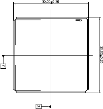
Getting to Know the ME909u-523
The package of the LGA module is 145 pin LGA with a dimension of 30 mm × 30 mm × 2.35
mm. It is applied to the user interface board, and can be used as a wireless terminal in a
network environment.
2
3
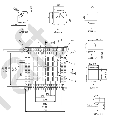
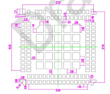
PCB Design
PCB Pad Design
To achieve assembly yields and solder joints of high reliability, it is recommended that the PCB
pad size be designed as follows: the sizes of the solder pads on customers' PCBs are the same
as those of the module's solder pads for the high production efficiency and high reliability of
solder joints. For details, see the following figure:
4
Requirements on PCB Layout
The thickness of PCB is more than 1.0 mm (1.2 mm recommended) to reduce the deformation
caused by high temperature welding.
The minimum distance between the LGA module and the PCB edge is 1.5 mm. Other devices
must be located more than 1 mm away from the LGA module (more than 3 mm recommended
if rework is considered).
When the PCB layout is double sided, it is recommended that the LGA module be placed on
the second side for assembly.
Design of Solder Mask
The PCB pad design can be solder mask defined (SMD), or non-solder mask defined
(NSMD).NSMD is recommended. In addition, the solder mask of the NSMD pad design is larger
than the pad so the reliability of the solder joint can be improved.
The solder mask must be 100 µm to150 µm larger than the pad, that is, the single side of the
solder mask must be 50 µm to 75 µm larger than the pad. The specific size depends on the
processing capability of the PCB manufacturer.
Assembly
Stencil Design
It is recommended that the stencil for the LGA module be 0.15 mm in thickness. For the stencil
design, see the following figure:
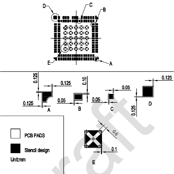
5
6
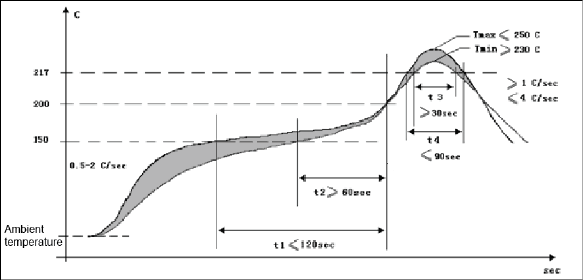
Reflow Profile
For the soldering temperature of the LGA module, see the following figure.
Reflow profile
7
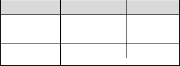
Reflow parameters
Temperature Zone Time Key Parameter
Preheat zone (40°C–150°C) 60s–120s Heating rate:
0.5°C/s–2°C/s
Soak zone
(150°C–200°C)
(t1–t2): 60s–120s Heating rate: < 1.0°C/s
Reflow zone (> 217°C) (t3–t4): 30s–90s Peak reflow temperature:
230°C–250°C
Cooling zone Cooling rate: 1°C/s ≤ Slope ≤ 4°C/s