Huawei Technologies MU509-65 HSDPA Module User Manual English
Huawei Technologies Co.,Ltd HSDPA Module English
Contents
- 1. UserManual.pdf
- 2. UserManual_Safety.pdf
UserManual.pdf

Copyright © Huawei Technologies Co., Ltd. 2015. All rights
reserved.
All rights reserved.
No part of this manual may be reproduced or transmitted in any form or by any means
without prior written consent of Huawei Technologies Co., Ltd. and its affiliates ("Huawei").
The product described in this manual may include copy righted software of Huawei and
possible licensors. Customers shall not in any manner reproduce, distribute, modify,
decompile, disassemble, decrypt, extract, rev erse engineer, lease, assign, or sublicense the
said sof tware, unless such restrictions are prohibited by applicable laws or such actions are
approved by respectiv e copy right holders.
Trademarks and Permissions
, , and are trademarks or registered trademarks of Huawei
Technologies Co., Ltd.
Other trademarks, product, serv ice and company names mentioned may be the property of
their respectiv e owners.
Notice
Some f eatures of the product and its accessories described herein rely on the software
installed, capacities and settings of local network, and theref ore may not be activ ated or
may be limited by local network operators or network serv ice prov iders.
Thus, the descriptions herein may not exactly match the product or its accessories which
y ou purchase.
Huawei reserv es the right to change or modify any inf ormation or specif ications contained in
this manual without prior notice and without any liability.
DISCLAIMER
ALL CONTENTS OF THIS MANUAL ARE PROVIDED “AS IS”. EXCEPT AS REQUIRED BY
APPLICABLE LAWS, NO WARRANTIES OF ANY KIND, EITHER EXPRESS OR IMPLIED,
INCLUDING BUT NOT LIMITED TO, THE IMPLIED WARRANTIES OF
MERCHANTABILITY AND FITNESS FOR A PARTICULAR PURPOSE, ARE MADE IN
RELATION TO THE ACCURACY, RELIABILITY OR CONTENTS OF THIS MANUAL.
TO THE MAXIMU M EXTENT PERMITTED BY APPLICABLE LAW, IN NO EVENT SHALL
HUAWEI BE LIABLE FOR ANY SPECIAL, INCIDENTAL, INDIRECT, OR
CONSEQUENTIAL DAMAGES, OR LOSS OF PROFITS, BUSINESS, REVENUE, DATA,
GOODWILL SAVINGS OR ANTICIPATED SAVINGS REGARDLESS OF WHETHER SUCH
LOSSES ARE FORSEEABLE OR NOT.
THE MAXI MUM LIABILITY (THIS LIMITATION SHALL NOT APPLY TO LIABILITY FOR
PERSONAL INJURY TO THE EXTENT APPLICABLE LAW PROHIBITS SUCH A
LIMITATION) OF HUAWEI ARISING FROM THE USE OF THE PRODUCT DESCRIBED IN
THIS MANUAL SHALL BE LIMITED TO THE AMOUNT PAID BY CUSTOMERS FOR THE
PURCHASE OF THIS PRODUCT.
Import and Export Regulations
Customers shall comply with all applicable export or import laws and regulations and be
responsible to obtain all necessary gov ernmental permits and licenses in order to export,
re-export or import the product mentioned in this manual including the software and
technical data therein.
i
Contents
Getting to Know the MU509-65 ................................................................................ 1
Dimension ..........................................................................................................................................................1
Position of RF Connectors..........................................................................................................................3
Pin Def initions ..................................................................................................................................................4
1
Thank you for purchasing HUAWEI MU509-65 WCDMA
Module (hereinafter referred to as the MU509-65)
Note:
This manual brief ly describes the dimension, the position of RF connectors and Pin
def initions.
You are recommended to read the manual bef ore using the MU509-65.
Getting to Know the MU509-65
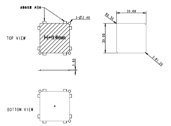
Dimension
The package of the WCDMA module is 145 pin with a dimension of 30 mm × 30 mm ×
2.57mm. It is applied to the user interf ace board, and can be used as a wireless
terminal in a network env ironment.
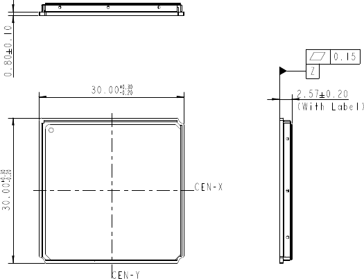
2
3
Position of RF Connectors
The WCDMA module prov ided one antenna connector (MAIN_AN T) f or connecting the
external antenna.
4
Pin Definitions
The sequence of MU509-65 interf ace is shown below.
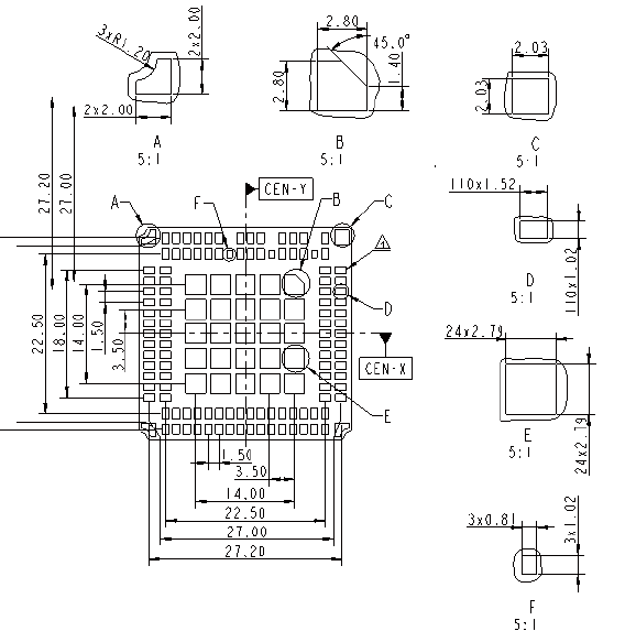
5
6
The Pin def initions of the MU509-65 interf ace is shown below.

7
Pin
No.
Pin Name
Pad Type
Description
Paramete r
Min.
(V)
Typ.
(V)
Max.
(V)
1
NC
-
Not connected
-
-
-
-
2
NC
-
Not connected
-
-
-
-
3
NC
-
Not connected
-
-
-
-
4
NC
-
Not connected
-
-
-
-
5
PCM_SYNC
O
PCM interface sync
VOH
2.15
-
2.6
VOL
0
-
0.45
6
PCM_DIN
I
PCM I/F data in
VIH
1.69
-
2.9
VIL
–0.3
-
0.91
7
PCM_DOU T
O
PCM I/F data out
VOH
2.15
-
2.6
VOL
0
-
0.45
8
PCM_CLK
O
PCM interfa ce clock
VOH
2.15
-
2.6
VOL
0
-
0.45
9
NC
-
Not connected
-
-
-
-
10
NC
-
Not connected
-
-
-
-
11
WAKEUP_I
N
I
Host to set the module into
sleep or wake up the module
from sleep.
VIH
1.69
-
2.9
VIL
–0.3
-
0.91
12
VBAT
PI
Power supply input
-
3.3
3.8
4.2
13
VBAT
PI
Power supply input
-
3.3
3.8
4.2
14
PS_HOLD
I
Used for JTAG interface
assigning a test point for it.
VIH
1.17
-
2.1
VIL
–0.3
-
0.63
15
Reserved
-
Reserved, please keep this
pin open.
-
-
-
-
16
NC
-
Not connected
-
-
-
-
17
NC
-
Not connected
-
-
-
-
18
NC
-
Not connected
-
-
-
-

8
Pin
No.
Pin Name
Pad Type
Description
Paramete r
Min.
(V)
Typ.
(V)
Max.
(V)
19
NC
-
Not connected
-
-
-
-
20
NC
-
Not connected
-
-
-
-
21
NC
-
Not connected
-
-
-
-
22
NC
-
Not connected
-
-
-
-
23
NC
-
Not connected
-
-
-
-
24
NC
-
Not connected
-
-
-
-
25
NC
-
Not connected
-
-
-
-
26
NC
-
Not connected
-
-
-
-
27
NC
-
Not connected
-
-
-
-
28
Reserved
-
Reserved, please keep this
pin open.
-
-
-
-
29
Reserved
-
Reserved, please keep this
pin open.
-
-
-
-
30
JTAG_TMS
I
JTAG test mode select
VIH
1.17
-
2.1
VIL
–0.3
-
0.63
31
VCC_EXT2
PO
2.6 V power output
-
2.5
2.6
2.7
32
VCC_EXT1
PO
1.8 V power output
-
1.65
1.8
1.95
33
NC
-
Not connected
-
-
-
-
34
USIM_VCC
PO
Power supply for USIM ca rd
-
1.65
1.8
1.95
-
2.7
2.85
3.0
35
VCOIN
PI
Coin cell input
-
1.5
3.0
3.25
36
JTAG_TRS T
_N
I
JTAG reset
VIH
1.17
-
2.1
VIL
–0.3
-
0.63
37
NC
-
Not connected
-
-
-
-
38
MIC2_P
I
Positive pole of the input of
audio interface 2.
-
-
-
-
39
MIC2_N
I
Negative pole of the input of
audio interface 2.
-
-
-
-
40
MIC1_P
I
Positive pole of the input of
audio interface 1.
-
-
-
-

9
Pin
No.
Pin Name
Pad Type
Description
Paramete r
Min.
(V)
Typ.
(V)
Max.
(V)
41
MIC1_N
I
Negative pole of the input of
audio interface 1.
-
-
-
-
42
JTAG_TCK
I
JTAG clock input
VIH
1.17
-
2.1
VIL
–0.3
-
0.63
43
Reserved
-
Reserved, please keep this
pin open.
-
-
-
-
44
GPIO
I/O
General Purpose I/O pin.
The function of these pins
has not been defined.
VOH
2.15
-
2.6
VOL
0
-
0.45
VIH
1.69
2.9
VIL
–0.3
0.91
45
GPIO
I/O
General Purpose I/O pin.
The function of these pins
has not been defined.
VOH
2.15
-
2.6
VOL
0
-
0.45
VIH
1.69
2.9
VIL
–0.3
0.91
46
GPIO
I/O
General Purpose I/O pin.
The function of these pins
has not been defined.
VOH
2.15
-
2.6
VOL
0
-
0.45
VIH
1.69
2.9
VIL
–0.3
0.91
47
NC
-
Not connected
-
-
-
-
48
GND
-
Ground
-
-
-
-
49
GND
-
Ground
-
-
-
-
50
GND
-
Ground
-
-
-
-
51
GPIO
I/O
General Purpose I/O pin.
The function of these pins
has not been defined.
VOH
2.15
-
2.6
VOL
0
-
0.45
VIH
1.69
2.9
VIL
–0.3
0.91
52
GND
-
Ground
-
-
-
-
53
GND
-
Ground
-
-
-
-
54
GND
-
Ground
-
-
-
-
55
GPIO
I/O
General Purpose I/O pin.
The function of these pins
has not been defined.
VOH
2.15
-
2.6
VOL
0
-
0.45
VIH
1.69
-
2.9
VIL
–0.3
-
0.91

10
Pin
No.
Pin Name
Pad Type
Description
Paramete r
Min.
(V)
Typ.
(V)
Max.
(V)
56
GND
-
Ground
-
-
-
-
57
GND
-
Ground
-
-
-
-
58
GND
-
Ground
-
-
-
-
59
GND
-
Ground
-
-
-
-
60
NC
-
Not connected
-
-
-
-
61
NC
-
Not connected
-
-
-
-
62
NC
-
Not connected
-
-
-
-
63
NC
-
Not connected
-
-
-
-
64
NC
-
Not connected
-
-
-
-
65
NC
-
Not connected
-
-
-
-
66
NC
-
Not connected
-
-
-
-
67
NC
-
Not connected
-
-
-
-
68
NC
-
Not connected
-
-
-
-
69
NC
-
Not connected
-
-
-
-
70
NC
-
Not connected
-
-
-
-
71
WAKEUP_O
UT
O
Module to wake up the host
VOH
2.15
-
2.6
VOL
0
-
0.45
72
JTAG_TD O
O
JTAG test data output
VOH
1.35
-
1.8
VOL
0
-
0.45
73
UART_DSR
O
UART Dat a Set Ready
VOH
2.15
-
2.6
VOL
0
-
0.45
74
UART_RTS
O
UART Ready for re ceive
VOH
2.15
-
2.6
VOL
0
-
0.45
75
UART_DCD
O
UART Dat a Carrier Detect
VOH
2.15
-
2.6
VOL
0
-
0.45
76
UART_TX
O
UART transmit output
VOH
2.15
-
2.6
VOL
0
-
0.45
77
UART_RING
O
UART Ring Indicator
VOH
2.15
-
2.6
VOL
0
-
0.45
78
UART_RX
I
UART receive data input
VIH
1.69
2.9
VIL
–0.3
0.91
79
UART_DTR
I
Data Terminal Ready
VIH
1.69
2.9
VIL
–0.3
0.91

11
Pin
No.
Pin Name
Pad Type
Description
Paramete r
Min.
(V)
Typ.
(V)
Max.
(V)
80
UART_CTS
I
UART Clear to Send
VIH
1.69
2.9
VIL
–0.3
-
0.91
81
POWER_ON
_OFF
I
System power-on or
power-off
VIH
1.17
-
2.1
VIL
–0.3
-
0.63
82
NC
-
Not connected
-
-
-
-
83
NC
-
Not connected
-
-
-
-
84
NC
-
Not connected
-
-
-
-
85
USB_DM
I/O
Full-speed USB D-
-
-
-
-
86
USB_DP
I/O
Full-speed USB D+
-
-
-
-
87
JTAG_TD I
I
JTAG test data input
VIH
1.17
-
2.1
VIL
–0.3
-
0.63
88
USIM_RES E
T
O
USIM reset
VOH
1.65/
2.7
1.8/
2.85
1.95/
3.0
VOL
0
-
0.36/
0.57
89
USIM_D AT
A
I/O
USIM data
VOH
1.65/
2.7
1.8/
2.85
1.95/
3.0
VOL
0
-
0.36/
0.57
VIH
1.65/
2.7
1.8/
2.85
1.95/
3.0
VIL
0
-
0.36/
0.57
90
USIM_CLK
O
USIM clock
VOH
1.65/
2.7
1.8/
2.85
1.95/
3.0
VOL
0
-
0.36/
0.57
91
LED_STATU
S
I
Status indicator
Current sink
Drive strength: 10 mA
-
-
-
-
92
NC
-
Not connected
-
-
-
-
93
JTAG_RTCK
I
JTAG return clock
VIH
1.17
-
2.1
VIL
–0.3
-
0.63
94
NC
-
Not connected
-
-
-
-
95
NC
-
Not connected
-
-
-
-

12
Pin
No.
Pin Name
Pad Type
Description
Paramete r
Min.
(V)
Typ.
(V)
Max.
(V)
96
EAR_OUT_
N
O
Negative pole of the output
of Earphone interface.
-
-
-
-
97
EAR_OUT_P
O
Positive pole of the output of
Earphone interface.
-
-
-
-
98
SPKR_OUT_
P
O
Positive pole of the output of
speaker interfa ce.
-
-
-
-
99
SPKR_OUT_
N
O
Negative pole of the output
of speaker interface.
-
-
-
-
100
RESIN_N
I
Reset module.
VIH
1.17
-
2.1
VIL
–0.3
-
0.63
101
LED_MOD E
I
Mode indicator
Current sink
Drive strength: 10 mA
-
-
-
-
102
NC
-
Not connected
-
-
-
-
103
NC
-
Not connected
-
-
-
-
104
NC
-
Not connected
-
-
-
-
105
GPIO
I/O
General Purpose I/O pin.
The function of these pins
has not been defined.
VOH
2.15
-
2.6
VOL
0
-
0.45
VIH
1.69
2.9
VIL
–0.3
0.91
106
GND
-
Ground
-
-
-
-
107
MAIN_ANT
-
RF main antenna pad
-
-
-
-
108
GND
-
Ground
-
-
-
-
109
GPIO
I/O
General Purpose I/O pin.
The function of these pins
has not been defined.
VOH
2.15
-
2.6
VOL
0
-
0.45
VIH
1.69
2.9
VIL
–0.3
0.91
110
GND
-
Ground
-
-
-
-
111
NC
-
Not connected
-
-
-
-
112
GND
-
Ground
-
-
-
-
113
GPIO
I/O
General Purpose I/O pin.
The function of these pins
has not been defined.
VOH
2.15
-
2.6
VOL
0
-
0.45
VIH
1.69
2.9
VIL
–0.3
0.91
114
GND
-
Ground
-
-
-
-

13
Pin
No.
Pin Name
Pad Type
Description
Paramete r
Min.
(V)
Typ.
(V)
Max.
(V)
115
NC
-
Not connected
-
-
-
-
116
GND
-
Ground
-
-
-
-
117
NC
-
Not connected
-
-
-
-
118
NC
-
Not connected
-
-
-
-
119
NC
-
Not connected
-
-
-
-
120
NC
-
Not connected
-
-
-
-
121
GND
-
Thermal Ground Pad
-
-
-
-
122
GND
-
Thermal Ground Pad
-
-
-
-
123
GND
-
Thermal Ground Pad
-
-
-
-
124
GND
-
Thermal Ground Pad
-
-
-
-
125
GND
-
Thermal Ground Pad
-
-
-
-
126
GND
-
Thermal Ground Pad
-
-
-
-
127
GND
-
Thermal Ground Pad
-
-
-
-
128
GND
-
Thermal Ground Pad
-
-
-
-
129
GND
-
Thermal Ground Pad
-
-
-
-
130
GND
-
Thermal Ground Pad
-
-
-
-
131
GND
-
Thermal Ground Pad
-
-
-
-
132
GND
-
Thermal Ground Pad
-
-
-
-
133
GND
-
Thermal Ground Pad
-
-
-
-
134
GND
-
Thermal Ground Pad
-
-
-
-
135
GND
-
Thermal Ground Pad
-
-
-
-
136
GND
-
Thermal Ground Pad
-
-
-
-
137
GND
-
Thermal Ground Pad
-
-
-
-
138
GND
-
Thermal Ground Pad
-
-
-
-
139
GND
-
Thermal Ground Pad
-
-
-
-
140
GND
-
Thermal Ground Pad
-
-
-
-
141
GND
-
Thermal Ground Pad
-
-
-
-
142
GND
-
Thermal Ground Pad
-
-
-
-
143
GND
-
Thermal Ground Pad
-
-
-
-
144
GND
-
Thermal Ground Pad
-
-
-
-
145
GND
-
Thermal Ground Pad
-
-
-
-