Huawei 01 正文 Module Power Supply Design Guide V100R001 02
HUAWEI Module Power Supply Design Guide-V100R001_02
HUAWEI_Module_Power_Supply_Design_Guide-V100R001_02
HUAWEI_Power_Supply_Guide
HUAWEI Module Power Supply Design Guide-(V100R001_02, English)
HUAWEI Module Power Supply Design Guide-(V100R001_02, English)
2015-02-27
使用手册: Huawei
Open the PDF directly: View PDF ![]() .
.
Page Count: 20
- Revision History
- Contents
- 1 Overview
- 2 Power Supply Requirements
- 3 Power Supply Design Requirements
- 4 External Power Supply Circuits
- 5 Recommendations for the Layout and Routing of External Power Supply Circuits
- 6 Acronyms and Abbreviations

HUAWEI Module
Power Supply Design Guide
Issue
02
Date
2014-11-07

Copyright © Huawei Technologies Co., Ltd. 2014. All rights reserved.
No part of this manual may be reproduced or transmitted in any form or by any means without prior written
consent of Huawei Technologies Co., Ltd. and its affiliates ("Huawei").
The product described in this manual may include copyrighted software of Huawei and possible licensors.
Customers shall not in any manner reproduce, distribute, modify, decompile, disassemble, decrypt, extract,
reverse engineer, lease, assign, or sublicense the said software, unless such restrictions are prohibited by
applicable laws or such actions are approved by respective copyright holders.
Trademarks and Permissions
, , and are trademarks or registered trademarks of Huawei Technologies Co., Ltd.
LTE is a trade mark of ETSI.
Other trademarks, product, service and company names mentioned may be the property of their respective
owners.
Notice
Some features of the product and its accessories described herein rely on the software installed, capacities
and settings of local network, and therefore may not be activated or may be limited by local network
operators or network service providers.
Thus, the descriptions herein may not exactly match the product or its accessories which you purchase.
Huawei reserves the right to change or modify any information or specifications contained in this manual
without prior notice and without any liability.
DISCLAIMER
ALL CONTENTS OF THIS MANUAL ARE PROVIDED “AS IS”. EXCEPT AS REQUIRED BY APPLICABLE
LAWS, NO WARRANTIES OF ANY KIND, EITHER EXPRESS OR IMPLIED, INCLUDING BUT NOT
LIMITED TO, THE IMPLIED WARRANTIES OF MERCHANTABILITY AND FITNESS FOR A PARTICULAR
PURPOSE, ARE MADE IN RELATION TO THE ACCURACY, RELIABILITY OR CONTENTS OF THIS
MANUAL.
TO THE MAXIMUM EXTENT PERMITTED BY APPLICABLE LAW, IN NO EVENT SHALL HUAWEI BE
LIABLE FOR ANY SPECIAL, INCIDENTAL, INDIRECT, OR CONSEQUENTIAL DAMAGES, OR LOSS OF
PROFITS, BUSINESS, REVENUE, DATA, GOODWILL SAVINGS OR ANTICIPATED SAVINGS
REGARDLESS OF WHETHER SUCH LOSSES ARE FORSEEABLE OR NOT.
THE MAXIMUM LIABILITY (THIS LIMITATION SHALL NOT APPLY TO LIABILITY FOR PERSONAL
INJURY TO THE EXTENT APPLICABLE LAW PROHIBITS SUCH A LIMITATION) OF HUAWEI ARISING
FROM THE USE OF THE PRODUCT DESCRIBED IN THIS MANUAL SHALL BE LIMITED TO THE
AMOUNT PAID BY CUSTOMERS FOR THE PURCHASE OF THIS PRODUCT.
Import and Export Regulations
Customers shall comply with all applicable export or import laws and regulations and be responsible to
obtain all necessary governmental permits and licenses in order to export, re-export or import the product
mentioned in this manual including the software and technical data therein.
Privacy Policy
To better understand how we protect your personal information, please see the privacy policy at
http://consumer.huawei.com/privacy-policy.
HUAWEI Module Power Supply Design Guide
About This Document
Issue 02 (2014-11-07)
Huawei Proprietary and Confidential
Copyright © Huawei Technologies Co., Ltd.
3
About This Document
Revision History
Document
Version
Date
Chapter
Descriptions
01
2011-10-12
Creation
02
2014-11-07
2.1
Updated the power pin of HUAWEI
modules
2.3
Updated power supply requirements in
not 2G mode
3.3
Added the type of the recommend
capacitor with high capacity
4.4
Added the type of the filtering capacitor

HUAWEI Module Power Supply Design Guide
Contents
Issue 02 (2014-11-07)
Huawei Proprietary and Confidential
Copyright © Huawei Technologies Co., Ltd.
4
Contents
1 Overview ................................................................................................................................... 5
2 Power Supply Requirements .................................................................................................. 6
2.1 Power Pin Definition .................................................................................................................... 6
2.2 Power Supply Requirements in 2G Mode .................................................................................... 6
2.3 Power Supply Requirements in not 2G Mode............................................................................... 8
2.4 Power Consumption .................................................................................................................... 9
3 Power Supply Design Requirements .................................................................................. 10
3.1 Introduction to Peripheral Power Supplies ..................................................................................10
3.2 Reducing Internal Resistance .....................................................................................................10
3.3 Adding Energy Storage Capacitors ............................................................................................. 11
3.4 Improving Transient Response of the Power Supply IC ...............................................................14
4 External Power Supply Circuits ........................................................................................... 16
4.1 Choosing the Power Supply IC ...................................................................................................16
4.2 Power Supply Protection ............................................................................................................16
4.3 Power-on and Power-off Sequences ..........................................................................................17
4.4 Choosing the Filtering Capacitor .................................................................................................18
5 Recommendations for the Layout and Routing of External Power Supply Circuits .... 19
6 Acronyms and Abbreviations ............................................................................................... 20

HUAWEI Module Power Supply Design Guide
Overview
Issue 02 (2014-11-07)
Huawei Proprietary and Confidential
Copyright © Huawei Technologies Co., Ltd.
5
1 Overview
This document mainly describes the power supply design for Huawei modules. This
document also provides Huawei modules' requirements for power supplies, which
can be used as reference for designing power supplies for Huawei modules. This
document is composed of four chapters:
- Power Supply Requirements
- Power Supply Design Requirements
- External Power Supply Circuits
- Recommendations for the Layout and Routing of External Power Supply Circuits
HUAWEI Module Power Supply Design Guide
Power Supply Requirements
Issue 02 (2014-11-07)
Huawei Proprietary and Confidential
Copyright © Huawei Technologies Co., Ltd.
6
2 Power Supply Requirements
2.1 Power Pin Definition
Table 2-1 The power pin of HUAWEI modules
HUAWEI Modules
Power Pin Name
Power Supply Voltage
LGA modules
VBAT
3.3 V–4.2 V (typically 3.8 V)
LCC modules
VBAT
3.3 V–4.2 V (typically 3.8 V)
Mini PCIe modules
VCC_3V3
3.0 V–3.6 V (typically 3.3 V)
M.2 modules
3.3V
3.135 V–4.4 V (typically 3.3 V)
All power supply pins and ground pins must be connected.
2.2 Power Supply Requirements in 2G Mode
This section describes the electrical characteristics of Huawei modules operating in
2G mode. The power consumption of Huawei modules is related to their transmitted
power (the transmitted power is the power that a wireless terminal transmits to a
base station, also known as uplink power). The greater the transmitted power, the
higher the power consumption.
The Global System for Mobile Communications (GSM) uses time division multiple
access (TDMA). Using this method, Huawei modules transmit power only during the
time slots allocated by base stations. In the GSM, each transmission period is divided
into eight time slots and each time slot lasts 577 µs. Modules transmit power during
one of the eight time slots. Therefore, the transmission period is 4.615 ms and the
transmission time is 577 µs in each transmission period. This transmission mode of
GSM wireless terminals is called "burst". The power transmitted by Huawei modules
during the allocated time slots is dependent on the received signal strength. The
stronger the received signal strength (the signal strength of the base station), the less
the transmitted power. The weaker the received signal strength, the greater the
transmitted power. The maximum transmitted power is 33 dBm (GSM-900).
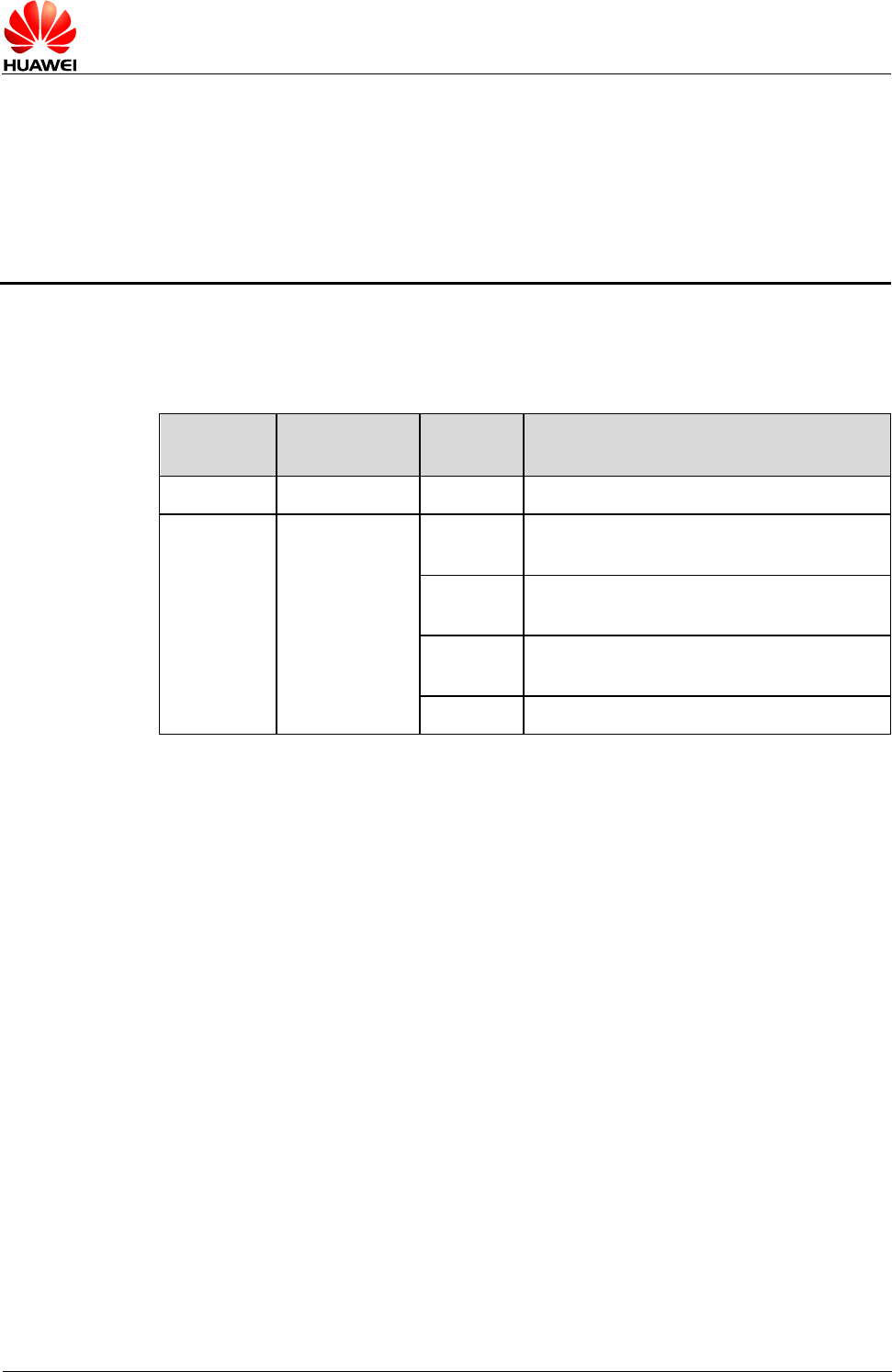
Figure 2-1 illustrates the power transmitting mode in GSM.
HUAWEI Module Power Supply Design Guide
Power Supply Requirements
Issue 02 (2014-11-07)
Huawei Proprietary and Confidential
Copyright © Huawei Technologies Co., Ltd.
7
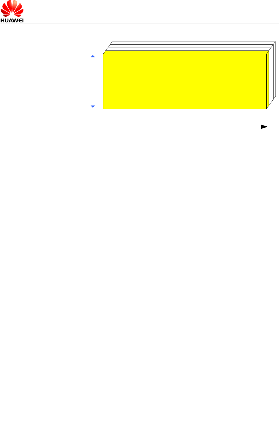
Figure 2-1 Power transmitting mode in GSM
577uS 577uS
577uS x 8 slot
4.61ms 4.61ms 4.61ms
Power
Max 33dBm
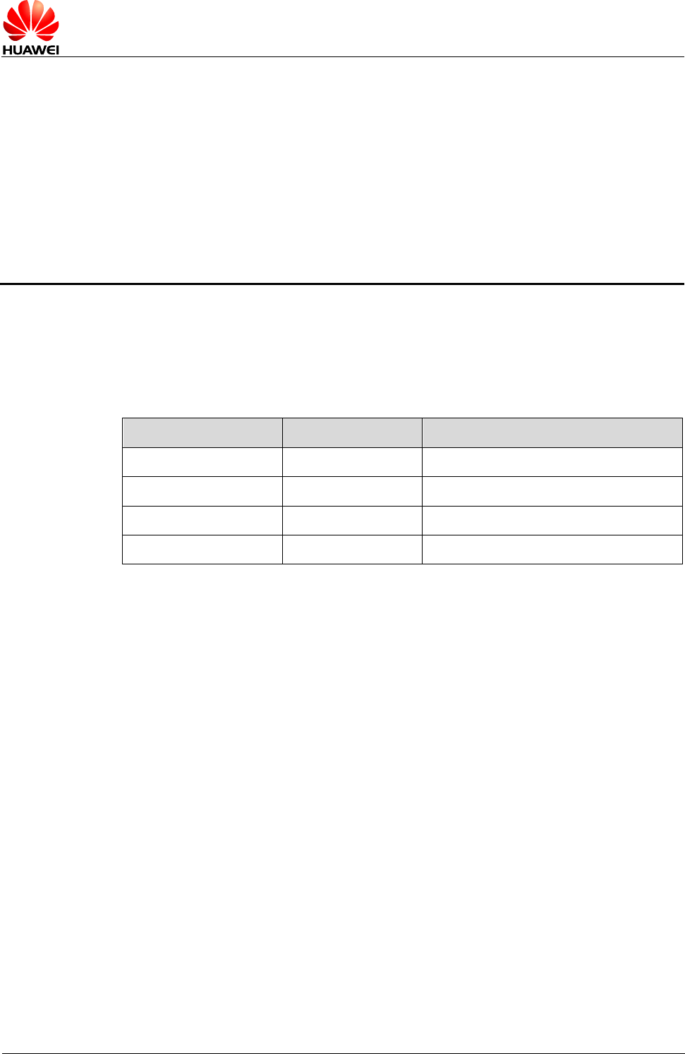
For general packet radio service (GPRS), the uplink transmission uses two or more
successive time slots, as illustrated in Figure 2-2 .
Figure 2-2 GPRS uplink transmission
577uS
577uS x 8 slot
4.61ms 4.61ms 4.61ms
Power
1.15ms
Max 30dBm
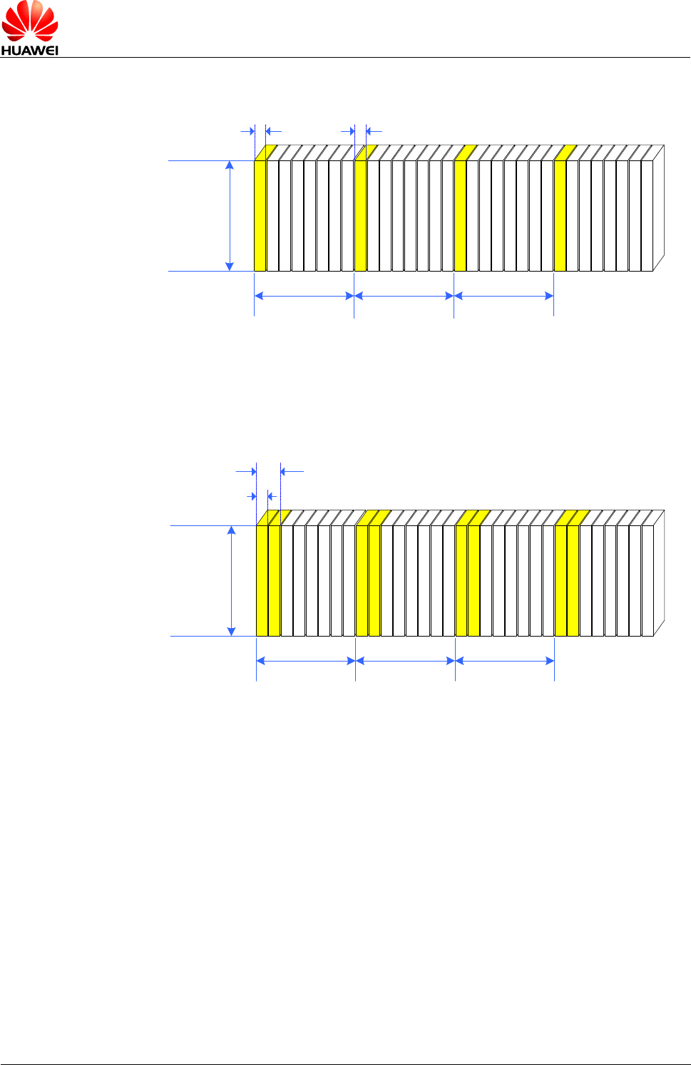
Because of the characteristics of TDMA used in GSM, Huawei modules' power
consumption changes periodically with bursts in accordance with the transmission
periods, as illustrated in Figure 2-3 .
HUAWEI Module Power Supply Design Guide
Power Supply Requirements
Issue 02 (2014-11-07)
Huawei Proprietary and Confidential
Copyright © Huawei Technologies Co., Ltd.
8
Figure 2-3 Huawei modules' power consumption changes
577uS 577uS
577uS x 8 slot
4.61ms 4.61ms 4.61ms
Power
Max 33dBm
Current- Ibat
Voltage-Vbat
Peak current
Max 2.5A
Dropout voltage
We can see from Figure 2-3 that during transmission time slots, the power amplifier
(PA) of the module's GSM unit amplifies power for transmission. If the received signal
strength is weak, the transmitted power may reach 33 dBm, and the transient electric
current supplied to the module can reach 2.5 A (IBAT). As a result, the power supply
voltage may drop.
The power supply voltage may drop, if:
- The power supply does not have good transient response performance and its
output cannot reach 2 A–3 A within several milliseconds.
- The internal resistor of the power supply (that is, the output impedance of the
power interface) is great. When the current is great, the voltage on the resistor
reduces outside the range specified by the module.
At the end of a transmission time slot, the PA shuts down, and the electric current
and voltage recover until the next transmission time slot comes after 4.615 ms.
Therefore, Huawei modules operating in 2G mode must have good transient
response performance and small internal resistance to prevent voltage drop.
Considering the product cost and that Huawei modules can operate within a certain
range of voltages, the minimum voltage of the power supply after dropping should not
be less than the minimum voltage specified by the module.
2.3 Power Supply Requirements in not 2G Mode
WCDMA and FDD-LTE telecommunications use code division multiple access
(CDMA). Therefore, on these networks, the transmitted power is not related to the
time.
Figure 2-4 shows the transmitted power of a Huawei module operating on the
WCDMA and FDD-LTE network.
HUAWEI Module Power Supply Design Guide
Power Supply Requirements
Issue 02 (2014-11-07)
Huawei Proprietary and Confidential
Copyright © Huawei Technologies Co., Ltd.
9
Figure 2-4 Transmitted power of the WCDMA and FDD-LTE system
time
Power
Max 24dBm
For Huawei modules operating on the WCDMA and FDD-LTE networks, when the
transmitted power reaches the maximum transmitted power, the required maximum
current from the power supply is approximately 1100 mA. Therefore, power supplies
with an average output of at least 1.5 A are required.
TD-SCDMA and TDD-LTE telecommunications use time division multiple access,
which is the same as GSM. But the transmitted power of TD-SCDMA and TDD-LTE is
much less than that of GSM, so their requirements of the power supply are the same
as WCDMA and FDD-LTE.
CDMA telecommunication uses code division multiple access, so its requirement of
the power supply is the same as WCDMA and FDD-LTE.
2.4 Power Consumption
Different Huawei modules have different power consumption, depending on their
platforms. For specific power consumption specifications and test conditions, refer to
the modules' hardware guides.

HUAWEI Module Power Supply Design Guide
Power Supply Design Requirements
Issue 02 (2014-11-07)
Huawei Proprietary and Confidential
Copyright © Huawei Technologies Co., Ltd.
10
3 Power Supply Design Requirements
3.1 Introduction to Peripheral Power Supplies
Peripheral power supplies provide power for Huawei modules. For Huawei modules
operating in GSM calls and GPRS data transmission on GSM networks, the
transmitted power of Huawei modules can reach 33 dBm (2 W). To prevent
unacceptable voltages drop, power supplies must have good transient response.
These factors must be considered for designing power supplies for Huawei modules.
When designing peripheral power supplies, focus on the following:
- Reducing Internal Resistance
- Adding Energy Storage Capacitors
- Improving Transient Response of the Power Supply IC
3.2 Reducing Internal Resistance
A main method to reduce the internal resistance of peripheral power supplies is to
use power supply integrated circuits (ICs) with the ability to output great currents. The
greater the output current, the smaller the internal resistance. Power supply ICs with
2.5 A outputs at minimum are recommended.
If using low-dropout (LDO) regulators in peripheral power supply ICs, use LDO
regulators with low dropout voltages. Because the input currents of LDO regulators
are equal to the output currents, LDO regulators with low dropout voltages are
equivalent to LDO regulators with small internal resistance.
If using DC-to-DC (DC-DC) converters in peripheral power supply ICs, pay attention
to the following switch parameters in the manuals: Negative Channel Metal-oxide
Semiconductor (NMOS) Switch On Resistance and Positive Channel Metal-oxide
Semiconductor (PMOS) Switch On Resistance. The switch on resistance must be
small. If peripheral diodes are required for the DC-DC power supply ICs, use
Schottky diodes with low voltage drop. The equivalent series resistance (ESR) of
peripheral power inductors for DC-DC power supply ICs must be as small as possible.
Minimize the power loss and internal resistance in the DC-DC power supply ICs.
HUAWEI Module Power Supply Design Guide
Power Supply Design Requirements
Issue 02 (2014-11-07)
Huawei Proprietary and Confidential
Copyright © Huawei Technologies Co., Ltd.
11
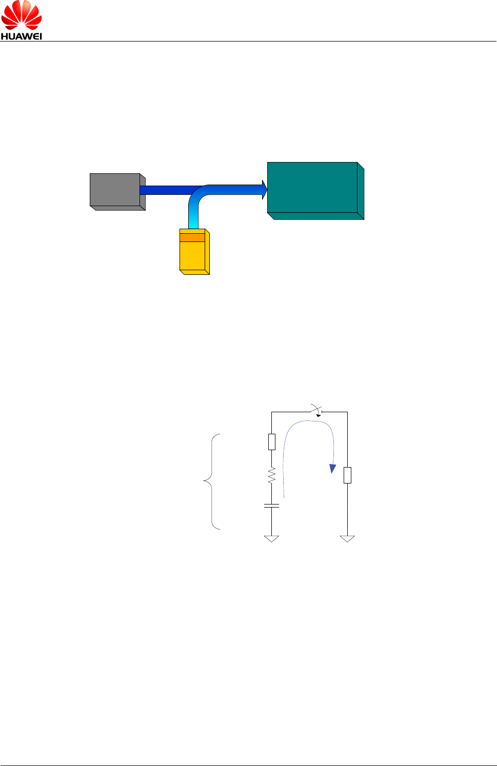
3.3 Adding Energy Storage Capacitors
If a peripheral power supply cannot provide a transient output of 2 A currents, you
must add a capacitor with sufficient capacitance to storage energy for current
compensation. See Figure 3-1 .
Figure 3-1 Add and energy storage capacitor
Power
supply
+
Vbat
A real capacitor is equivalent to the combination of one ideal capacitor (C), one
equivalent series inductance (ESL) and one ESR that are connected in series. Figure
3-2 illustrates the model of a real capacitor.
Figure 3-2 Model of a real capacitor
t1 :close
ESL
ESR
C
R lo a d
Ipeak
t2 :open
Model of a real capacitor
Assume that the original voltage on the ideal capacitor is Vo and the peak current is
Ipeak. When the power supply switch is turned off, the capacitor starts to release
electric charge. Before the switch is turned on, the voltage on the load (Vload) can be
calculated using the following formula:
Vload = Vo – (ESR x Ipeak) – (ESL x Ipeak/ΔtL) – (Ipeak x Δt/C)
= Vo – VESR – VESL – VC.
In the previous formula, the voltage drop (VESL) caused by the ESL only occurs and
exists at moments when the switch is turned on or off. Δt is the time for the current
changes from 0 to Ipeak, usually lasting several µs. When the current is stable, VESL is
0. The ESL of ceramic capacitors and tantalum capacitors is very small and can be
ignored. The ESL of aluminum electrolytic capacitors is large because aluminum
HUAWEI Module Power Supply Design Guide
Power Supply Design Requirements
Issue 02 (2014-11-07)
Huawei Proprietary and Confidential
Copyright © Huawei Technologies Co., Ltd.
12
electrolytic capacitors have long pins. Therefore, aluminum electrolytic capacitors are
not recommended. In addition, note that ESL also exists on the traces connecting the
capacitor pins and the power supply. To reduce the voltage drop caused by ESL, the
traces should be as wide as possible.
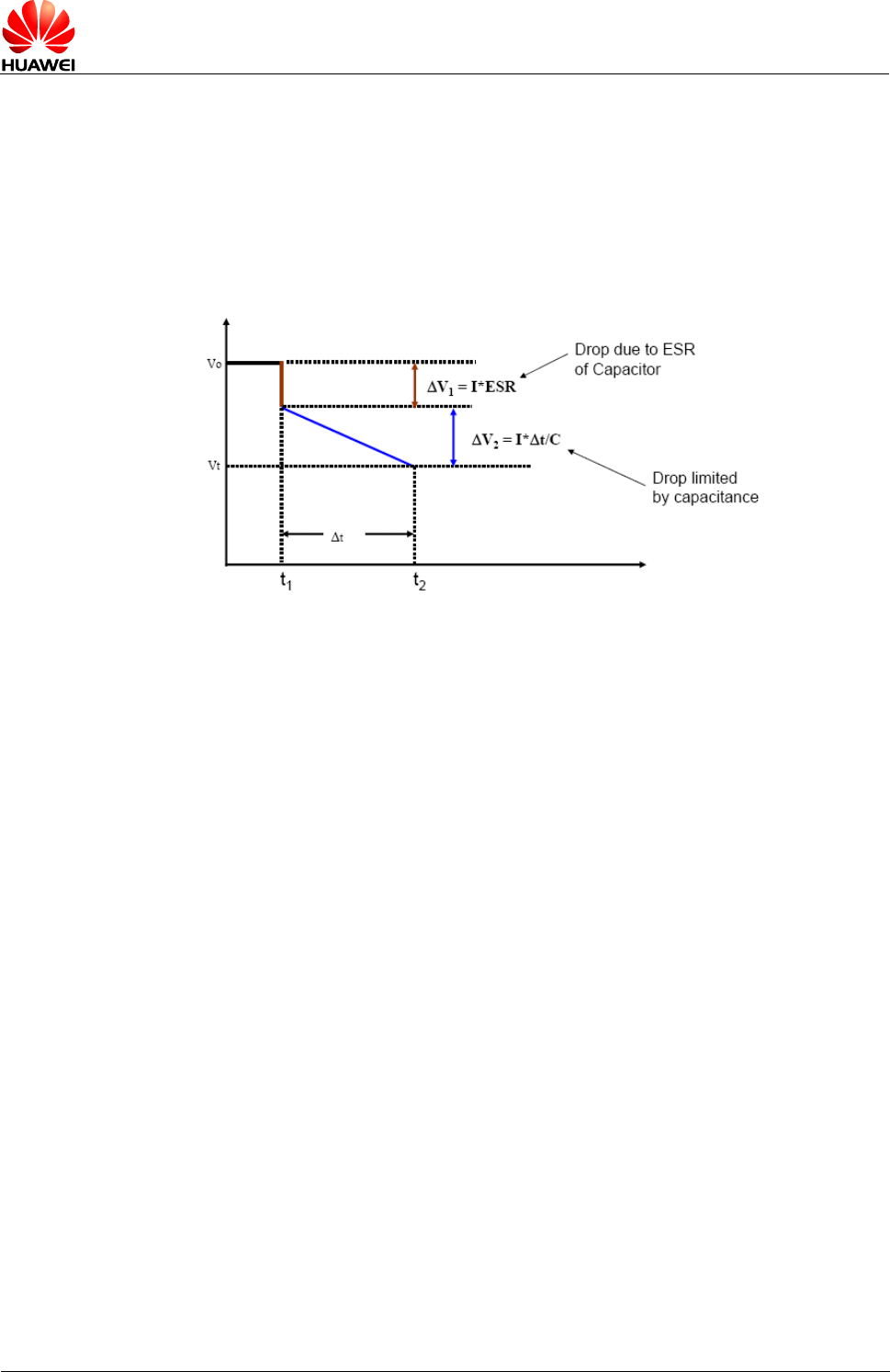
Unlike VESL, VESR and VC cause voltage drop throughout the peak current duration.
Figure 3-3 shows a simple analysis of VESR and VC.
Figure 3-3 Simple analysis of VESR and VC
Vdrop = (ESR x Ipeak) + (Ipeak x Δt/C)
From the previous formula, we can infer that the greater the ESR of capacitors, the
greater the voltage drop. Therefore, capacitors with small ESR should be used. We
can also infer that the smaller the capacitance, the greater the voltage drops.
Therefore, capacitors with large capacitance should be used.
Capacitors with ESR smaller than 0.1 Ω should be used (note that aluminum
electrolytic capacitors have large ESR and are not recommended).
The following describes how to calculate the capacitance of the decoupling capacitor
used in the power supply for a Huawei module operating on a GSM network. Assume
that t1 is the time when the voltage starts to drop, which is also the time when the PA
of the Huawei module starts amplifying power. Assume that t2 is the time when the
PA of the Huawei module stops amplifying power. Then the duration between t1 and
t2 is a time slot during which the power is transmitted. For GSM, Δt = t2 – t1 = 577 µs,
which is equal to a transmission time slot. For GPRS class 10, Δt = t2 – t1 = 577 µs x
2 = 1.15 ms, corresponding to two transmission time slots.
Provided that a capacitor with 0.1 Ω ESR is used, then Ipeak = 2.5 A (at maximum
power) and Δt = 1.15 ms.
Then the voltage drop caused by ESR is:
VESR = ESR x Ipeak = 0.1 Ω x 2.5 A = 0.25 V.
The discharge process of capacitors is a differential process, so:
Vc = Ipeak x Δt/C = 2.5 A x 0.00115/C = 0.0029/C.
Vdrop = 0.25 + 0.0029/C.
Provided that the allowed maximum Vdrop is 0.3 V, then C = 58 mF.
HUAWEI Module Power Supply Design Guide
Power Supply Design Requirements
Issue 02 (2014-11-07)
Huawei Proprietary and Confidential
Copyright © Huawei Technologies Co., Ltd.
13
Obviously, 58 mF is too large. This is the result of a model in which the voltage drop
is compensated only by the capacitor and the power supply IC is ignored. The
previous calculation should be revised based on the conditions in real application.
The result also reveals that the ESR must be smaller. Currently, the minimum ESR of
tantalum capacitors is about 0.05 Ω. If smaller ESR is required, use capacitors
connected in parallel. For example, if we use AVX's TCJB157M006R0070 (150 µF,
6.3 V; nominal ESR: 0.07 Ω) and connect ten such capacitors in parallel, then the
capacitance of these ten capacitors is equivalent to 1500 µF and the ESR is
equivalent to 0.007 Ω.
Δt is related to the transient response duration of the power supply IC. Provided that
the transient response duration of the power supply IC is 100 µs (that is, the power
supply IC can output a 2 A current in 100 µs), then the valid period for current
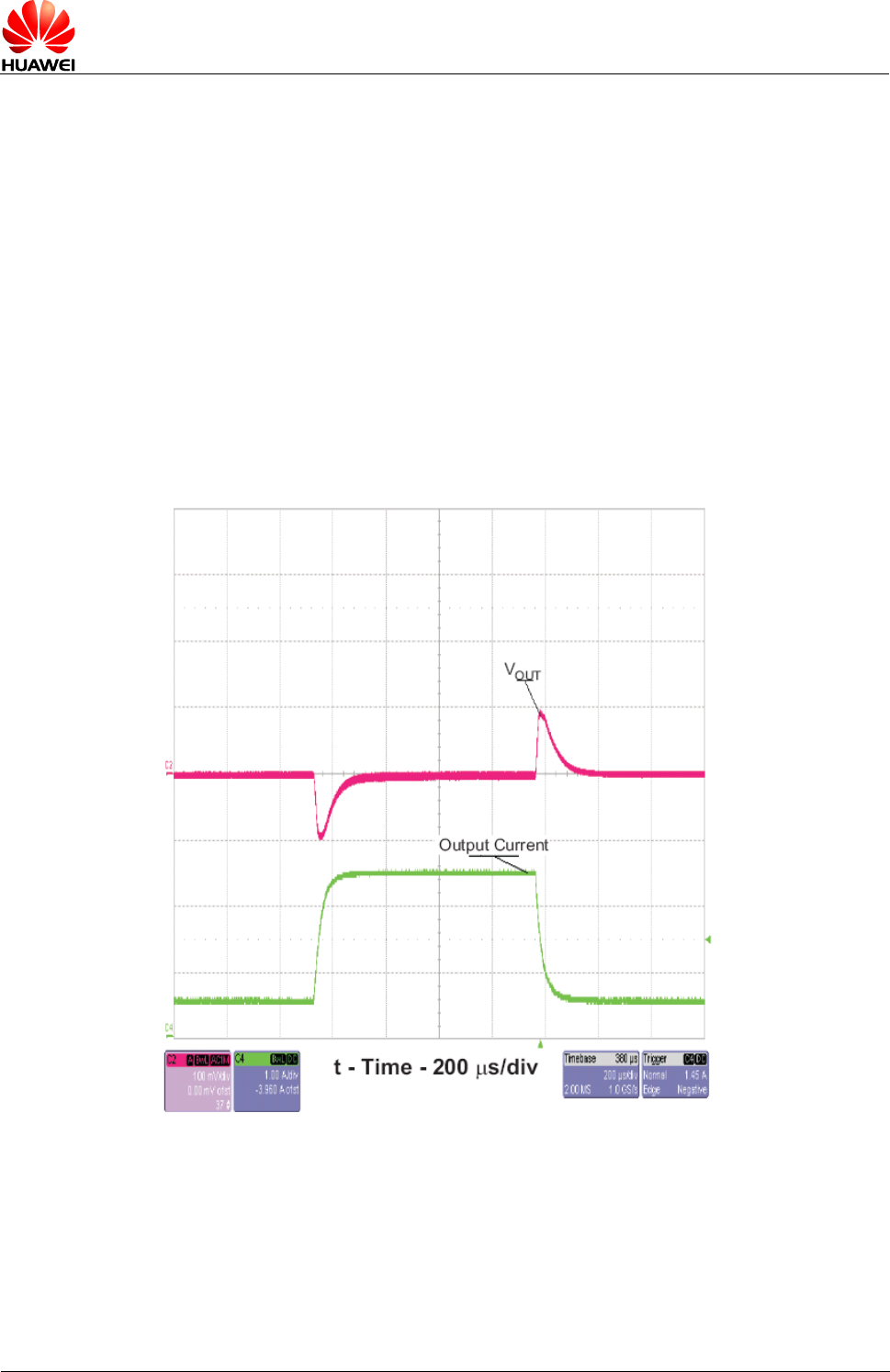
compensation from the capacitors is 100 µs. Figure 3-4 shows the transient response
performance of a power supply IC.
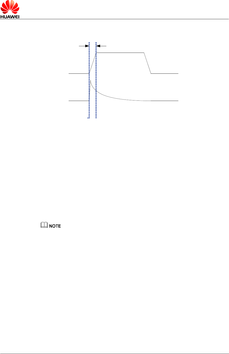
Figure 3-4 Transient response performance of a certain power supply IC
From Figure 3-4 we can discern that when the transient current suddenly reaches 2 A,
the response duration is about 50 µs. Therefore, the capacitors need to compensate
the current only during this 50 µs. Obviously, Δt is approximately equal to the
transient response duration of the power supply IC.
HUAWEI Module Power Supply Design Guide
Power Supply Design Requirements
Issue 02 (2014-11-07)
Huawei Proprietary and Confidential
Copyright © Huawei Technologies Co., Ltd.
14
Figure 3-5 Transient response duration
IpowerIC
Icap
Transient response duration: t
Figure 3-5 illustrates that the peak current is provided by the compensation current
(Icap) from the capacitors when the power supply IC is in the transient response
duration. After the transient response duration, the capacitors can stop the output
current. Note that Figure 3-5 does not consider the case that the power supply IC will
charge the capacitors after the transient response duration.
In conclusion, if ten 150 µF capacitors are connected in parallel and Δt = 100 µs, then:
Vdrop = (ESR x Ipeak) + (Ipeak x Δt/C)
= (0.007 x 2.5 A) + (2.5 A x 0.0001/0.0015)
= 0.184 V
Vdrop is smaller than 0.3 V, meeting the requirement.
The previous calculation does not consider the transient response of the component that
supplies power to the power supply IC. Therefore, Δt should have a greater value in actual
applications.
From the previous description, we can see that the voltage drop is dependent on the
ESR, transient response duration of the power supply (Δt), and capacitance of the
capacitors. Therefore, the capacitance, ESR, ESL and transient response duration
must be taken into account during the power supply design.
For different network modes, it is all recommended to use four (at least two) TDK
ceramic capacitors (C3216X5R0J107MT0A0N with 1206 package). Its capacitance is
100 μF and withstand voltage is 6.3 V.
3.4 Improving Transient Response of the Power Supply IC
In actual application scenarios, the transient response duration of peripheral power
supply ICs must be determined. Designers need to obtain the information about the

HUAWEI Module Power Supply Design Guide
Power Supply Design Requirements
Issue 02 (2014-11-07)
Huawei Proprietary and Confidential
Copyright © Huawei Technologies Co., Ltd.
15
transient response duration from the manual of the power supply ICs to be used. The
shorter the transient response duration, the smaller the capacitance of energy
storage capacitors can be.
Connecting a large capacitor to the input to the power supply IC can also improve the
transient response of the IC. If the transient response of the component that supplies
power to the power supply IC is slow, the transient power supply cannot be ensured
even though the power supply IC has fast transient response.

HUAWEI Module Power Supply Design Guide
External Power Supply Circuits
Issue 02 (2014-11-07)
Huawei Proprietary and Confidential
Copyright © Huawei Technologies Co., Ltd.
16
4 External Power Supply Circuits
4.1 Choosing the Power Supply IC
Huawei modules can be used in many application scenarios. Different application
scenarios have different requirements. Therefore, the following requirements are
provided for reference only.
- Requirements for DC-DC converters
Currents of modules operating in GSM mode changes a lot in a very short
moment, and the input voltages of modules also fluctuate greatly. Therefore, DC-
DC converters selected must have fast transient response.
- Operating temperature
Pay attention to the ambient temperature in the operating environment of
modules. Make sure that the ambient temperature is appropriate. It is not
recommended that the modules be used under temperature exceeding their
rated operating temperature.
- Derate the power supplies' voltages and currents before using them (85% of
original ratings is recommended).
Either DC-DC converters or LDO regulators can be used for supplying power to
Huawei modules.
4.2 Power Supply Protection
The components of Huawei modules, such as the PA, are designed for using one Li-
ion battery. These components are sensitive to high voltages. To provide stable
voltages, two-stage power supplies are preferred, that is, reduce the voltages output
from DC-DC power supply ICs before they are input to LDO regulators; then LDO
regulators supply power to modules. If two-stage power supplies cannot be used due
to environmental restrictions, protection should be provided for the power supply
systems of modules. Figure 4-1 shows a power supply protection circuit.
HUAWEI Module Power Supply Design Guide
External Power Supply Circuits
Issue 02 (2014-11-07)
Huawei Proprietary and Confidential
Copyright © Huawei Technologies Co., Ltd.
17
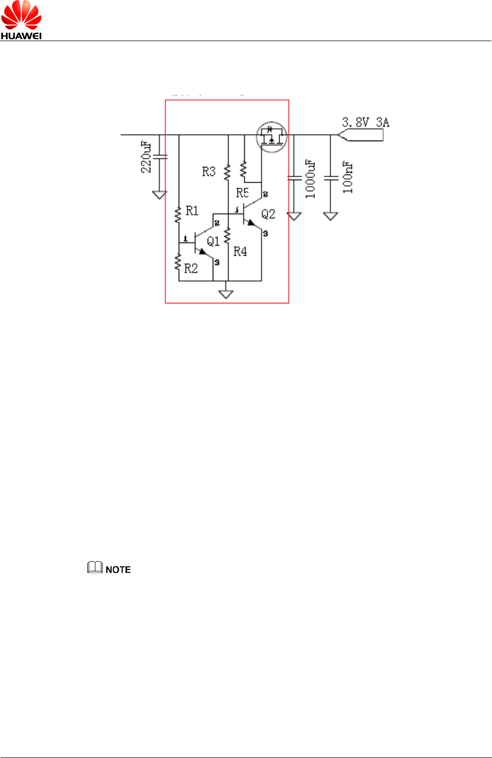
Figure 4-1 Power supply protection circuit
Power supply protection circuit
Power supply
input
When the input voltages are within the normal range:
Use the 3.8 V input voltage as an example. The voltage on electrodes of Q1 is
obtained from the voltage split by R1 and R2. Make sure that the Q1 electrode
voltage is not high enough to turn on Q1. The voltage on electrodes of Q2 is obtained
from the voltage split by R3 and R4. Make sure that the Q2 electrode voltage is high
enough to turn on Q2. After Q2 is turned on, the PMOS transistor on the main power
supply line is turned on and the power is supplied to the module.
When the input voltages are not within the normal range:
Use the 4.3 V input voltage as an example. The voltage on electrodes of Q1 is
obtained from the voltage split by R1 and R2. Make sure that the Q1 electrode
voltage is high enough to turn on Q1. Make sure that the Q2 electrode voltage is not
high enough to turn on Q2 after Q1 is turned on. After Q2 is turned off, the PMOS
transistor on the main power supply line is turned off. This provides overvoltage
protection for the module.
Figure 4-1 is a schematic. Except the components marked with parameters, all components in
the schematic must be selected based on specific applications. When selecting components,
consider the temperature impact on the turn-on voltages for the base and emitter of a triode.
4.3 Power-on and Power-off Sequences
For Huawei modules, the power-on and power-off sequences are more important.
Before the modules are completely powered on, do not perform controls and

HUAWEI Module Power Supply Design Guide
External Power Supply Circuits
Issue 02 (2014-11-07)
Huawei Proprietary and Confidential
Copyright © Huawei Technologies Co., Ltd.
18
communications of modules, and do not apply high voltages to the modules' control
signals; doing so may cause the modules cannot power on or power off.
4.4 Choosing the Filtering Capacitor
The energy storage capacitors with high capacity are recommended to use at least
three TDK ceramic capacitors (C3216X5R0J107MT0A0N with 1206 package). Its
capacitance is 100 μF and withstand voltage is 6.3 V.
And according to the circuit recommended by HUAWEI, capacitors with different
capacity (such as 100 nF, 33 pF and 22 μF) should be added for filtering of different
frequencies.

HUAWEI Module Power Supply Design Guide
Recommendations for the Layout and
Routing of External Power Supply Circuits
Issue 02 (2014-11-07)
Huawei Proprietary and Confidential
Copyright © Huawei Technologies Co., Ltd.
19
5 Recommendations for the Layout and
Routing of External Power Supply Circuits
Recommendations for the layout and routing of external power supply circuits include:
- Arrange the input bypass capacitors for the DC-DC converter as close as
possible to the input pin of the power supply IC. Arrange the output capacitors as
close as possible to the inductors. This can suppress ripples effectively. Route
power supply traces as wide as possible, to meet the requirement for providing
great current when the transmitted power is great.
- The filtering capacitor for the VBAT power supply should be as close as to the
power pin of the module.
- Connect diodes that can protect against overvoltage and reverse connection to
the connector through which external power supply is provided. This can protect
power supply circuits in abnormal situations.
- Arrange the inductor as close as possible to the output pins of the power supply
IC. The traces connecting the power IC and the inductor must be as short as
possible, to avoid switch interference.
- Route all signal traces at least 2 mm away from the area under the power supply
IC's power inductors and large-current diodes. Traces of sensitive analog signals
and clock signals must be at least 5 mm away from power inductors, to reduce
interference.
- Use two different traces for the power ground and the signal ground, and use
single-point grounding. Ensure that the current on a ground return does not flow
to the signal ground.
- If modules are used in harsh environment, reverse voltage protection is required
for external power supply circuits.
HUAWEI Module Power Supply Design Guide
Acronyms and Abbreviations
Issue 02 (2014-11-07)
Huawei Proprietary and Confidential
Copyright © Huawei Technologies Co., Ltd.
20
6 Acronyms and Abbreviations
Acronym or abbreviation
Expansion
3GPP
3rd Generation Partnership Project
CDMA
Code Division Multiple Access
DC/DC
Direct Current to Direct Current
ESL
Equivalent Series Inductance
ESR
Equivalent Series Resistance
GPRS
General Packet Radio Service
GSM
Global System of Mobile communication
LDO
Low Dropout Regulator
LGA
Land Grid Array
LTE
Long Term Evolution
NMOS
Negative Channal Metal-oxide semiconductor
PA
Power Amplifier
PCB
Printed Circuit Board
PMOS
Positive Channal Metal-oxide Semiconductor
WCDMA
Wideband Code Division Multi Access
TDMA
Time Division Multiple Access
TD-SCDMA
Time Division-Synchronous Code Division
Multiple Access
