IP Mobilenet IPB800 Base Station User Manual 369548
IP Mobilenet, LLC Base Station 369548
UserManual.wiki
>
IP Mobilenet
>
IPB800 User Manual
>
Owners Manual
Contents
1.
Owners Manual
2.
Users Manual
Owners Manual
Navigation menu
Upload a User Manual
Namespaces
Wiki Guide
HTML
PDF
Info
Views
User Manual
Discussion / Help
Navigation
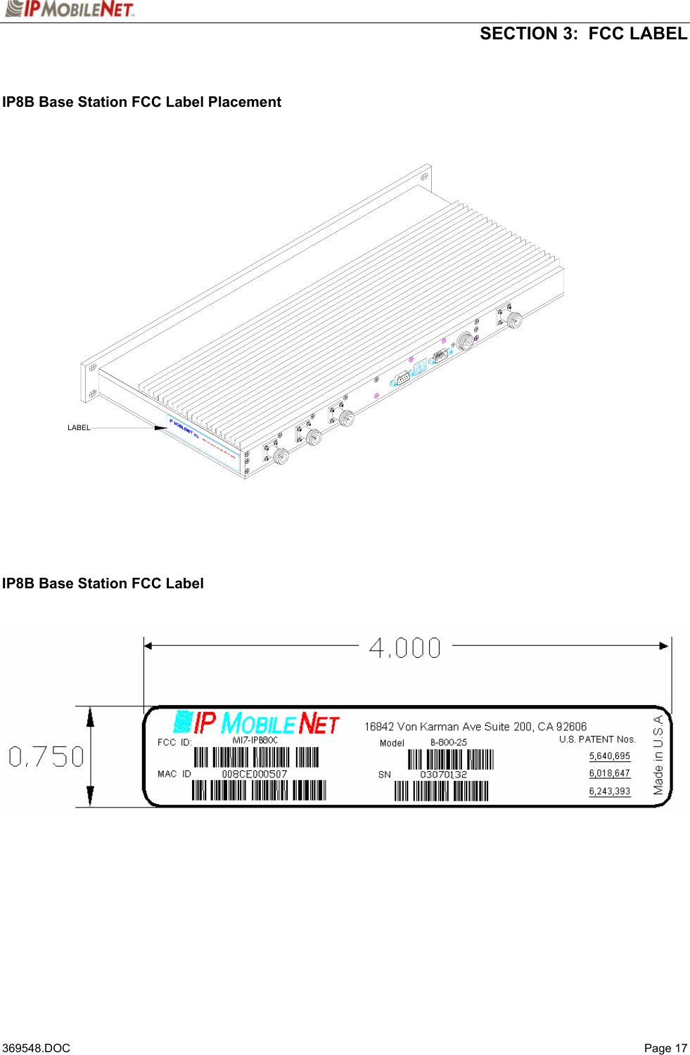
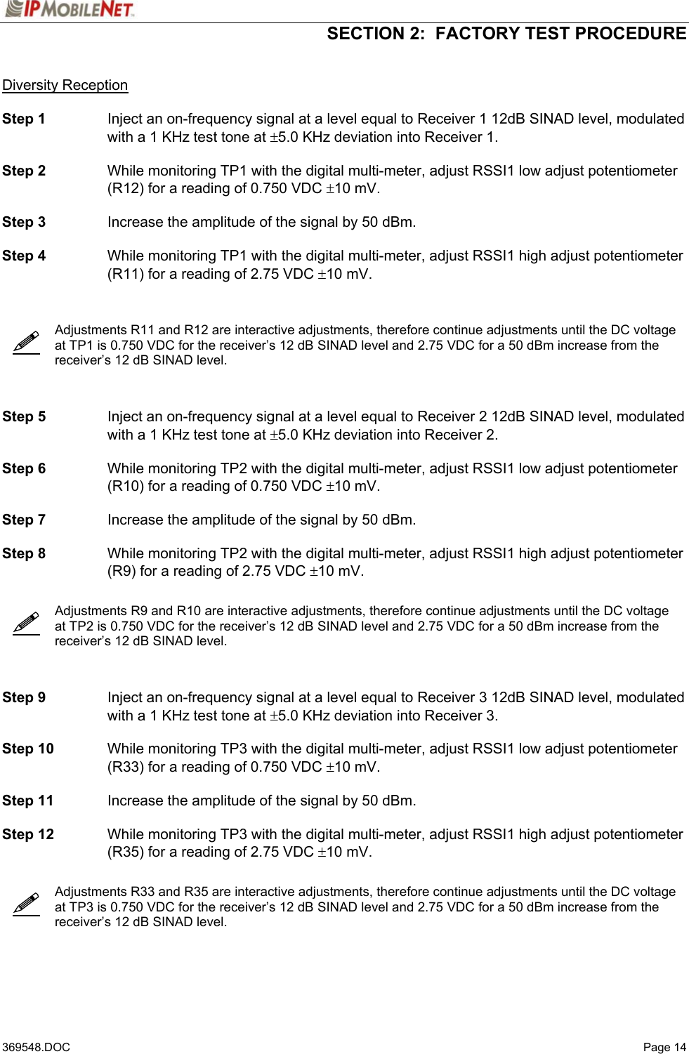
![SECTION 2: FACTORY TEST PROCEDURE 369548.DOC Page 12 Programming and Configuring the Base Station This section applies to the 851-866 frequency range of the IPSeries Base Station. Important! The base station’s IP address must be known prior to performing the procedures in this section. The programming procedure should be performed when it is necessary to upgrade a base station’s Firmware or to change the operating parameters to suit client needs. Viewing the Base Station’s Configuration Data Step 1 At the HyperTerminal window, type in the appropriate password and press [ENTER]. Step 2 Type ? and press [ENTER]. The following example displays in the HyperTerminal window: Host serial = 115200,N,8,1, timeout=200 Host framing = SLIP, no split frames no status messages tunnel = 0 TX format = new Injection = LOW SIDE, 45MHz channel spacing = 25000 Channel = 0 Channel Tx freq Rx freq Inj freq Frequency=0 , 815.100000, 860.100000, 815.100000 Serial number: yyyyyyyyy RIM address = 1 Frequency group = 1 TX quiet time = 5 Symbol sync time = 12 milliseconds, 0 extra inter-split-frame count TX tail time = 5 Radio data rate = 19200 Max data tx time = 60 seconds Carrier detect delay time = 1 millisecond Station ID = ABC123 Station ID time =10 minutes Polarity = TX+, RX+ Allow crc errors = 0 Suppress keep alive = 0 Allow base to base = 0 Timeslot status = 0 Duplicate time = 10 milliseconds Control head grant delay = 50 milliseconds RIM DD delay = 0 milliseconds Retry interval = 0 milliseconds Retry time limit = 0 milliseconds RSSI step = 25 (=19dBm) IPNC = 192.168.3.3 SLIP Address = 192.168.4.6 RF IP Address = 192.168.3.1 SNTP interval = 60 seconds num timeslots = 16 timeslot period = 992ms timeslots per voice packet = 4 noise = -128dBm Fixed TX Delay = 0 milliseconds Scale TX Delay = 0 microseconds](https://usermanual.wiki/IP-Mobilenet/IPB800.Owners-Manual/User-Guide-369548-Page-13.png)
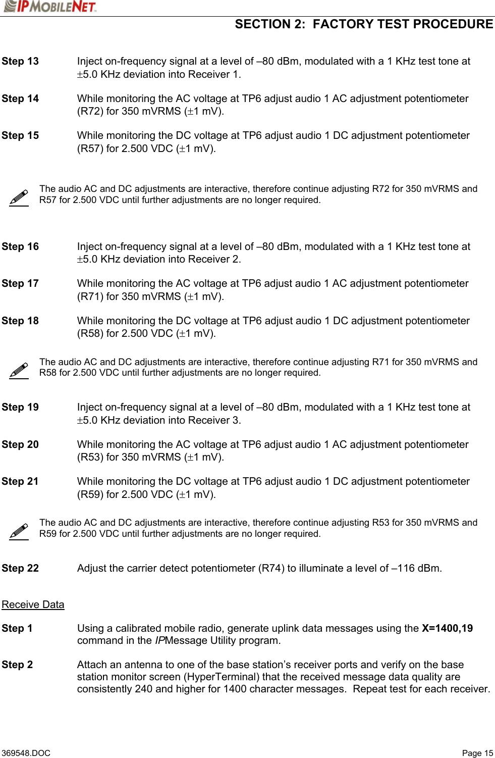
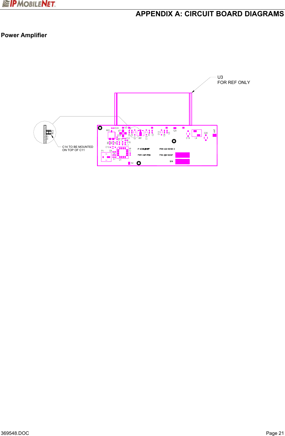
![SECTION 2: FACTORY TEST PROCEDURE 369548.DOC Page 16 Exciter Step 1 Using the X=1400,19 command, generate data messages so the transmit power and frequency can be checked. Step 2 Note the power level and then on the power amplifier circuit board adjust the potentiometer (R3) fully counterclockwise (this will enable low power transmit operation). Step 3 Connect the base stations’ transmit port to the HP communication test set. Step 4 While transmitting data messages using the X=1400,19 command, adjust the following: TCXO Y1 for minimum frequency error R42 for ±5 KHz deviation Transmit output power should be approximately 1mWatt. The REFMOD adjustment needs to be made while the base station is transmitting real data messages to and from a mobile radio. This is most easily done using the ping command to ping the IPNC from a mobile radio. This will cause the base station to repeatedly send data messages and will facilitate the REFMOD adjustment. Step 5 Connect the base station to the IPNC. Step 6 Using a calibrated mobile radio operating on the base station’s channel, adjust R30 for consistent data quality readings of 248 (as observed on the mobile radio’s attached PC IPMessage window). Access the MSDOS prompt and ping using the following command: >;ping 192.168.3.3 –t –l 500 –w 2000 This command will ping the IPNC continuously with a 500-character test message. Press [Ctrl]+C to stop the ping. Power Amplifier Step 1 Connect the base station’s transmit port to the communication test set. Step 2 Using the X=1400,19 command, generate data messages. Step 3 Slowly increase the base station output power by turning the power control potentiometer clockwise until the power noted in Step 2. Do not exceed 20 watts output power, as this will reduce the life of the amplifier module. If the base station uses a power amplifier, output power must be set to achieve power output specified for the specific base station installation. Step 4 Perform a close visual inspection of the base station paying close attention to manufacturing related problems such as loose screws, solder practices, etc.](https://usermanual.wiki/IP-Mobilenet/IPB800.Owners-Manual/User-Guide-369548-Page-17.png)