IP Mobilenet IPMNDT45TX 400-512MHz Mobile Data Radio User Manual 281739
IP Mobilenet, LLC 400-512MHz Mobile Data Radio 281739
Manual

4
40
00
0
–
–
5
51
12
2
M
MH
Hz
z
M
Mo
ob
bi
il
le
e
D
Da
at
ta
a
R
Ra
ad
di
io
o
O
Ow
wn
ne
er
r’
’s
s
M
Ma
an
nu
ua
al
l
Date Prepared:
March 1, 2000
-
Document Control #: DC-94
Version: C-1 (Special Release)
Copyright 2000-2002 IPMobileNet, Inc.
16842 Von Karman Avenue, Suite 200 Irvine, CA 92606
Voice: (949) 417-4590 Fax: (949) 417-4591

TABLE OF CONTENTS
~\Technical Documentation\System Manuals\FCC-Reports\DT450-FCCRpt.doc Page 2
SECTION 1: THEORY OF OPERATION ................................................................................. 3
General Block Diagram................................................................................................ 3
General Block Diagram Definitions..................................................................... 3
DT450 Mobile Data Radio Board Circuitry ......................................................... 5
Microcontroller....................................................................................... 5
Support Circuitry ......................................................................... 5
Input/Output .......................................................................................... 5
Injection Synthesizer ............................................................................. 6
Transmitter ............................................................................................ 6
Receiver 1 Front-End ............................................................................ 6
Receiver 1 IF......................................................................................... 7
Transmit Processing ............................................................................. 7
Baseband Routing................................................................................. 8
Power and Ground ................................................................................ 8
Receiver 2 Front-End ............................................................................ 8
Receiver 2 IF......................................................................................... 9
Modem .................................................................................................. 9
SECTION 2: FACTORY TEST PROCEDURE ....................................................................... 10
Equipment List ........................................................................................................... 10
Programming and Configuring Mobile Data Radio ................................................. 11
Adjustment / Alignment Procedures ........................................................................ 12
Receiver Injection............................................................................................. 12
Receiver 1
........................................................................................................ 12
Receiver 2
........................................................................................................ 13
Transmitter ....................................................................................................... 14
Power Setting ................................................................................................... 16
SECTION 3: LABEL AND LABEL PLACEMENT ................................................................ 17
DT450 Mobile Data Radio FCC Label Placement..................................................... 17
DT450 Mobile Data Radio FCC Label........................................................................ 17
APPENDIX A: DT450 MOBILE DATA RADIO CIRCUIT BOARD DIAGRAM....................... 18
SECTION 1: THEORY OF OPERATION
~\Technical Documentation\System Manuals\FCC-Reports\DT450-FCCRpt.doc Page 3
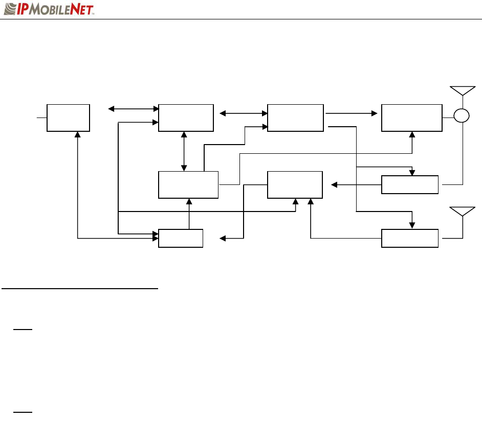
General Block Diagram
General Block Diagram Definitions
For increased data security, the modem supports the U.S. Government developed Digital Encryption
Standard (DES) data encryption and decryption protocols. This capability requires installation of third
party, Internet Protocol (IP) compliant DES encryption and decryption software on the system.
The standard IP circuit board contains ten (10) sections defined below.
These added sections will be discussed in Section 4 of this document.
Input/Output Circuitry associated with the radio’s DB25 data connector providing all the
RS232 data and handshake functions, including the necessary level
changes.
Microcontroller Manages the operation of the radio loading the selected transmit/receive
frequencies into the injection synthesizer, controls the operation of the
modem, and determines which receiver provides a better signal from a
given transmission. Also provides transmit time-out protection in the event
a fault causes the radio to halt in the transmit mode.
Transmit Processing Circuitry that amplifies the analog audio signal from the modem and uses it
to modulate the voltage controlled oscillator (VCO) and 10 MHz reference
oscillator in the injection synthesizer section. Modulating the VCO and
reference oscillator simultaneously results in a higher quality FM signal.
Modem Converts parallel data into an analog audio waveform for transmission and
analog audio from the receiver to serial data. Serial data appears on the
radio’s RS232 port, which connects a Mobile Data Computer (MDC) or a
Voice Interface Unit (VIU).
Input /
Output
D
DA
AT
TA
A
Micro-
Controller
Injection
Synthesizer
Transmitter
Transmit
Processing
Baseband
Routing Receiver 1
Receiver 2 Modem

SECTION 1: THEORY OF OPERATION
~\Technical Documentation\System Manuals\FCC-Reports\DT450-FCCRpt.doc Page 4
The modem supports a 115.2 Kbps data transmission rate on the serial
port, SLIP protocol, and up to 19.2 Kbps over-the-air rate. Within a single
chip it provides forward error correction and detection, bit interleaving for
more robust data communications, and third generation collision detection
and correction capabilities.
Injection Synthesizer Provides programmable, ultra stable signals for the radio. One synthesizer
incorporates phase lock loop technology used for both receiving and
transmitting.
High Side Injection In the receive mode, the synthesizer provides a local oscillator signal of 45
MHz above the selected receive channel frequency.
Low Side Injection In the receive mode, the synthesizer provides a local oscillator signal of 45
MHz below the selected receive channel frequency.
In the DT450, due to limitations in synthesizer frequency coverage, high
side injection is used for receive frequencies below 456 MHz.
Low side injection is used for all other receive frequencies. In the
transmit mode, the desired frequency is produced, and it is directly
modulated by the modem. A 10 MHz reference oscillator controls the
synthesizer.
Baseband Routing Allows the microcontroller to select one of the two diversity receiver audio
outputs for demodulation by the modem. Switching is done by the
microcontroller comparing the Received Signal Strength Indication (RSSI)
outputs from each receiver. Provision is also made for switching an
external modulation source from the DB25 data connector to the
transmitter input.
Transmitter Consists of an exciter and power amplifier module. The transmitter covers
the various frequency bands in segments. A different power amplifier
module is required for each segment. The transmitter circuitry includes a
T/R switch, switching the antenna between transmitter and receiver 1
(TX/RX1).
Receiver 1/Receiver 2 Required to support the mobile DRS; two (2) discrete receivers are tuned
to the same channel and use two (2) antennas.
The receivers are double-conversion superheterodyne with a first
Intermediate Frequency (IF) of 45 MHz and a second IF frequency of 455
KHz. Each receiver consists of bandpass filters, RF amplifiers, a crystal
filter, a double-balanced mixer, and a one-chip IF system. The injection
synthesizer provides the first local oscillator signal. Outputs from each
receiver include RSSI and analog audio for the baseband routing circuitry
and modem.
Power Supply Consists of circuitry that derives the various operating voltages for the
radio. A group of fixed and adjustable voltage regulators are used for this
purpose. The transmitter power control circuitry is also found in this
section.

SECTION 1: THEORY OF OPERATION
~\Technical Documentation\System Manuals\FCC-Reports\DT450-FCCRpt.doc Page 5
DT450 Mobile Data Radio Board Circuitry
The DT450 Mobile Data Radio works within a frequency range of 400 to 512 MHz.
The following section provides detail views and key areas on the DT450 Mobile Data Radio circuit board
especially useful during troubleshooting.
Microcontroller
The microcontroller (U43) is a major component of the radio as it manages the operation of the radio
loading the selected transmit/receive frequencies into the injection sythesizer. It also controls the
operation of the modem, and determines which receiver provides a better signal from a given
transmission. It provides transmit time-out protection in the event a fault causes the radio to halt in the
transmit mode. It utilizes a Reduced Instruction Set Computer (RISC) architecture which provides low
power operation and a powerful instruction set. Other features include a watchdog timer, serial UART,
two 8-bit timers, and 2 kB of electrically erasable programmable read only memory (EEPROM) storage.
The EEPROM RAM stores the setup data entered by the technician even if there is a loss of power.
Support circuitry
The support circuitry consists of the following:
A Supervisor Control Chip (U4) providing power-on reset.
The clock controls microcontroller operation and is generated by crystal Y4 and a Pierce oscillator
circuit (inside the U43-microcontroller).
The latch (U40) decodes low order address bits (A0-A7) from the address/data bits (AD0-AD7). It
enables Address Latch Enable (ALE) output of U43 and the bits are used by the modem and
synthesizer circuitry.
A 32Kx8 Static RAM Chip (U41) provides temporary storage of the radio’s configuration data
facilitating the technician with access to make changes.
Glue logic is also an important part in the microcontroller section. The RAM chip select (CS) and
modem chip select (MODEMCS*) command lines are created by U46. These gates decode four (4)
high order address bits (A11-A15), plus the read (RD*) and write (WR*) command lines.
Input/Output
Input/output components convert serial and handshake data from the modem section to RS232 levels,
and vice-versa. Chip U47 is an RS232 transmitter and receiver. It converts data in 5-volt logic form to
data in +/-12-volt form, as required by the RS232 standard. A charge pump power supply on the chip
converts the +5-volt DC logic power on pin 16 to the +12-volt and –12-volt levels required utilizing
capacitors C199-C202 to generate these voltages.

SECTION 1: THEORY OF OPERATION
~\Technical Documentation\System Manuals\FCC-Reports\DT450-FCCRpt.doc Page 6
Injection Synthesizer
The synthesizer chip (U3) is the major contributor of the injection synthesizer. This device contains the
key components of a phase locked loop (PLL), including a 1.1 GHz prescaler, programmable divider, and
phase detector. The selected frequencies are loaded into U3 as a clocked serial bit stream via the PLL
DATA and PLL CLOCK inputs. The microcontroller provides the serial data.
A 10 MHz reference frequency is provided by voltage controlled, temperature compensated crystal
oscillator module (VCTCXO)(Y3). This device has an input (REFMOD) that accepts transmit modulation
and voltage from a RX FREQ ADJUST pot RV3. The pot allows the receiver to be fine-tuned to the exact
operating frequency.
Diode (D1), capacitor (C34), and inverter (U44E) form a lock indication circuit. For troubleshooting, a
green light emitting diode (LED) D5 glows and indicates the synthesizer is locked and working properly.
The UHF signal is generated by a wide-range voltage controlled oscillator (VCO) module VCO1. A
voltage on the VT input determines the VCO frequency. The voltage is generated by the phase detector
output (PDOUT) of U3 driving a loop filter consisting of R4, C33, C23, R3, and C32. It integrates the
pulses that normally appear on PDOUT into a smooth DC control signal for the VCO. During transmit, the
analog signal from the modem and transmit processing circuitry is applied to VCO1 via the VCOMOD
input.
The output of VCO1 RFOUT goes to a two-way power divider (U30). One port of the U30 passes through
a 3V attenuator (AT1) and provides the transmit injection (TXINJ) signal for the transmitter circuit while
the other port drives another two-way power divider (U31). The first port of U30 provides the receive
injection (RXINJ2) signal for Receiver 2, while the second port output is boosted by wide-band amplifier
(U32). The amplifier output provides the receive injection (RXINJ1) signal for Receiver 1.
Transmitter
The transmitter section consists of an exciter, power amplifier, and power control circuitry. The exciter is
built around an RF power amplifier chip (U28). To transmit, 5-volt power is applied to the 5VKEY line.
This causes the U28 to power up and amplify the TXINJ signal. A gain control circuit inside of the U28
maintains the output power level to a constant value throughout the UHF spectrum. Simultaneously, the
12VKEY line is powered up. This causes power amplifier (U1) to boost the RF power to the desired level.
Up to 40 watts are available from the transmitter.
The power amplifier modules are self-contained hybrid devices that contain both active and passive
circuitry. There are five (5) modules available and each covers a 20-to-30 MHz portion of the UHF band.
Should replacement of U1 be required, the exact replacement part must be used.
Receiver 1 Front-End
This section consists of the components that form Receiver 1 Front-End. These components include a
T/R switch, bandpass filters, RF amplifiers, and a mixer circuit.
SW1 is a hybrid monolithic device that serves as the T/R switch and protects the Receiver from RF
damage by isolating it from the transmitter output. SW1 is normally in the receive position. At the start of
a transmission, a control voltage is applied to the TRSWCNTL input and SW1 transfers the antenna to
the transmitter power amplifier.
SECTION 1: THEORY OF OPERATION
~\Technical Documentation\System Manuals\FCC-Reports\DT450-FCCRpt.doc Page 7
Incoming signals pass through a double-tuned filter (FT4A) that selectively provides a high degree of out-
of-band signal rejection. A low noise amplifier (U6A) amplifies the selected signals and a triple-tuned filter
(FT3A) provides additional selectivity. An RF amplifier chip (Q6A) further amplifies the signal. The output
from Q6A passes through another triple-tuned filter (FT2A) and it goes to the mixer (U29A). U29A is a
double-balanced mixer which heterodynes the receive injection (RXINJ1) signal from the synthesizer with
the RF amplifier output. The result is a 45 MHz IF signal. Spurious signals are filtered out by FL5A, a 4-
pole bandpass filter, and the IF signal goes to the Receiver 1 IF section for further processing.
There are five (5) filter sets (FT2A, FT3A, and FT4A) available, and each one covers a 20-30 MHz portion
of the UHF band. Should replacement of the filters be required, exact replacement parts must be used.
Receiver 1 IF
This section consists of Receiver 1 IF subsystem. The major contributor of the IF subsystem is a
complete 45 MHz superheterodyne receiver chip that contains an RF amplifier, mixer, local oscillator, 455
KHz IF, quadrature detector, and received signal strength indication (RSSI) detector (U8A).
Incoming 45 MHz signals appearing at ISTIF pass through an amplifier and an LC matching circuit to a
mixer. A crystal oscillator is controlled by crystal Y1A and provides the injection frequency for the mixer.
This signal drives the oscillator in the Receiver 2 IF subsystem. The mixer output passes through a 455
KHz ceramic filter (FL6A). It is then amplified and passed through another ceramic filter (FL7A) to a
second gain stage. The IF output drives a quadrature detector. The recovered audio appears at pin 9 of
U8A. The RSSI detector converts the AGC voltage generated inside the chip into a DC level
corresponding logarithmically to the signal strength. The Diversity Reception Controller uses RSSI to
select the receiver with the best quality signal.
High frequency deemphasis is provided by a filter consisting of a resistor (R416) and a capacitor (C378).
The audio is amplified by op amps (U9AC and U9AA) and delivered to the baseband routing circuitry via
the BRXMOD1 output. Pot R19A is necessary to adjust the DC levels of U9AC and U9AA output.
Transmit Processing
The analog circuitry in this section modulates the Transmitter. There is also a fine-tuning frequency
adjustment for the Receiver.
The data-bearing audio signal from the modem appears at TXMOD. The audio is amplified by op amp
(U10A) and the DC output voltage of U10A is simultaneously biased to about half of the supply voltage by
the VBIAS input. VBIAS biases the other op amps in the same manner so they operate in a linear region.
This is necessary because these op amps operate from a single power supply. The output of U10A
passes through a low pass filter (R31) and the signal drives two (2) amplifiers.
The upper amplifier (U39B) has adjustable gain. The output drives op amp (U39A), which inverts the
phase of the signal allowing the modulated signal to pass through to the 10 MHz reference oscillator in
the synthesizer. Some makes of 10 MHz oscillators do not require the modulation signal to be inverted
and a jumper block (JMP1) is provided to accommodate the oscillators. The lower op amp (U10B)
amplifies the signal from the low pass filter and applies it to the VCO via the VCOMOD output.

SECTION 1: THEORY OF OPERATION
~\Technical Documentation\System Manuals\FCC-Reports\DT450-FCCRpt.doc Page 8
Baseband Routing
This circuitry selects audio from the appropriate receiver to route to the modem for demodulation.
Power and Ground
Power from the vehicle’s battery appears at the VBATT pad. The supply line powers a series of voltage
regulators and the transmitter control circuitry, as follows:
Voltage regulator VR3 provides a continuous 5-volts for the microcontroller, RS232 interface, and
modem circuitry. This power supply is always live allowing user-defined parameters to be stored in
the radio.
Voltage regulator VR5 provides switched 8-volt power for most other sections in the radio. VR1 is
switched on by the microcontroller.
Voltage regulator VR6 powers the analog circuitry in the radio.
In the transmit control circuitry, to transmit, the microcontroller makes TXKEYOUT* low. This causes Q5
to conduct, grounding the gate terminal of Q2. This forces the P-channel device to conduct, applying 5-
volts via 5VKEY to the transmitter exciter. At the same time Q4 conducts, grounding the gate terminal of
Q7. This forces the P-channel device to conduct, applying 12-volts via 12VKEY to the transmitter power
amplifier.
Transmitter over-temperature protection is provided by a temperature sensor (U18). When the heatsink
becomes too hot, U18 shunts the bias from transistors Q5 and Q4 to ground, turning off Q2 and Q7. This
shuts down the transmitter. After the heatsink cools off, the shunt is removed and transmission can
resume.
Receiver 2 Front-End
The circuitry for Receiver 2 is identical to Receiver 1 with the exception of the T/R switch and an
additional amplifier (U33).
Incoming signals pass through a filter (FT4B). The filter is a double-tuned device that provides a high
degree of selectivity. Selected signals are amplified by a low noise amplifier (U6B). A triple-tuned filter
(FT3B) provides additional selectivity and the signal is further amplified by an RF amplifier chip (Q6B).
The output from Q6B passes through another triple-tuned filter (FT2B) and it goes to a double-balanced
mixer (U29B), which heterodynes the amplified signal from U33. The result is a 45 MHz IF signal.
Spurious signals are filtered out by a 4-pole bandpass filter (FL5B). The IF signal goes to Receiver 2 IF
for further processing.
There are five (5) filter sets (FT2B, FT3B, and FT4B) available and each one covers a 20-30 MHz
portion of the UHF band. Should replacement of the filters be required, exact replacement parts
must be used.
Receiver 2 IF

SECTION 1: THEORY OF OPERATION
~\Technical Documentation\System Manuals\FCC-Reports\DT450-FCCRpt.doc Page 9
This section is identical to the Receiver 1 IF with the exception of the local oscillator circuitry.
Incoming 45 MHz signals appearing at 2NDIF pass through an amplifier and an LC matching circuit
mixer. Local oscillator injection is provided by the Receiver 1 IF subsystem. The mixer output passes
through a 455 KHz ceramic filter (FL6B). It is then amplified and passed through another ceramic filter
(FL7B) to a second gain stage. The IF output drives a quadrature detector. The recovered audio
appears at pin 9 of U8B. The RSSI detector converts if the amplifier current is generated inside the chip
into a DC level corresponding logarithmically to the signal strength. RSSI is used by the Diversity
Reception Controller to select the Receiver with the better quality signal.
Modem
The IP uses a single-chip modem circuit (U49) that converts parallel data to an analog audio waveform
for transmission and analog audio from a receiver to serial data. In addition to the modem functions, U49
provides forward error correction and detection, bit interleaving for more robust data communications, and
third generation collision detection and correction capabilities.
The microcontroller section controls the Modem operation. Address bus (A0 and A1), address/data bus
(A0-A7), and control lines (RD*, WR*, MODEMCS*) operate the Modem chip. The Modem circuitry
requires a crystal-controlled clock, consisting of crystal Y5 and an internal Pierce oscillator.
Incoming audio from the baseband routing circuit appears on the DISCAUD input. The audio signal is
demodulated into digital data appearing on the AD0-AD7 lines when the MODEMCS* and RD* lines are
low. The data goes to the microcontroller section for further processing, and then to the input/output
section for conversion to RS232 signal levels. At this point, the received data is available to the user’s
MDC and VIU.
During a transmission, outgoing data appearing on the AD0-AD7 lines is converted into a 4-level FSK
audio signal by the modem chip. This operation takes place when the MODEMCS* and WR* lines are
low. Data from the user’s MDC or VIU passes through the input/output section and microcontroller
section to the AD0-AD7 bus.
This modem supports 115.2 KBPS (serial port) and 19.2 KBPS or 9600 KBPS (over-the-air) data
transmission rates.

SECTION 2: FACTORY TEST PROCEDURE
~\Technical Documentation\System Manuals\FCC-Reports\DT450-FCCRpt.doc Page 10
Equipment List
The following table lists the equipment required to perform the DT450 Mobile Data Radio Factory Test
Procedure:
QTY DESCRIPTION MANUFACTURER MODEL
2
PC’s
One for Mobile
One for Base
Windows 9X w/
IPMessage
AVR
1 Service Monitor – Communication Test
Set HP HP890 or
equivalent
1 Digital multi-meter Tektronix
Fluke
77 or
equivalent
1 DC power supply w/ ammeter, 13.8V,
12 Amps or more Astron VS12M or
equivalent
1 4-Channel Scope Tektronix TDS 460A
1 DR4B Calibrated Base Station
1 Internet Protocol Network Controller
(IPNC)
1 100 watt dummy load/attenuator Pasternack PE7021-40 or
equivalent
2 UHF Antennas (generic mag mount)
1 Serial cable DB25M-DB25F
connectors
1 DT power cable
1 3-foot RF jumper cable with type N
connectors (generic)
1 Scope test probe (generic, X1
attenuation)
1 Ceramic tuning tool IPMN p/n:
44010006
1 ea #0, #1, and #2 Phillips screwdrivers
(generic)

SECTION 2: FACTORY TEST PROCEDURE
~\Technical Documentation\System Manuals\FCC-Reports\DT450-FCCRpt.doc Page 11
Programming and Configuring the Mobile Data Radio
Once the appropriate equipment for performing the factory test are gathered, perform the following steps
to program and configure an DT450 Mobile Data Radio:
Step 1 Enter the following information on the Mobile Data Radio Performance Test Data Sheet:
Radio Serial number
Date test being performed
Tester's Name
Step 2 Program the radio to the current Firmware revision using the AVR programming utility.
Step 3 Connect a PC to the radio using IPMessage program. In the IPMessage window, type in the
following command:
factory default
Press the [ENTER] key and the radio will load default configuration values into the
IPMessage window.
Step 4 Enter the appropriate values for the radio's frequency band.
[To: Radio] ?
[From: 192.168.3.10] Host serial = 19200,N,8,1, timeout=200
[From: 192.168.3.10] Host framing =
[From: 192.168.3.10] SLIP no status messages
[From: 192.168.3.10] Injection = LOW SIDE, 45MHz
[From: 192.168.3.10] channel spacing = 25000
[From: 192.168.3.10] Channel = 0
[From: 192.168.3.10] TX Power = 0
[From: 192.168.3.10] Car to car TX power = 0
[From: 192.168.3.10] Channel Tx freq Rx freq Inj freq
[From: 192.168.3.10] Frequency=0 , 486.000000, 481.000000, 436.000000
[From: 192.168.3.10] Serial number: undefined
[From: 192.168.3.10] TX quiet time = 5
[From: 192.168.3.10] TX sync time = 12 milliseconds, 0 extra inter-split-frame count
[From: 192.168.3.10] TX tail time = 5
[From: 192.168.3.10] Radio data rate = 19200
[From: 192.168.3.10] Max data tx time = 60 seconds
[From: 192.168.3.10] PLL load to txkey delay = 2 milliseconds
[From: 192.168.3.10] Carrier detect delay time = 3 milliseconds
[From: 192.168.3.10] Polarity = TX-, RX+
[From: 192.168.3.10] allow crc errors = 0
[From: 192.168.3.10] Duplicate time = 10 milliseconds
[From: 192.168.3.10] RSSI step = 12 (=234mV)
[From: 192.168.3.10] noise = -62dBm, -131dBm
[From: 192.168.3.10] Fixed TX Delay = 0 milliseconds
[From: 192.168.3.10] Scale TX Delay = 0 microseconds
[From: 192.168.3.10] IP Address = 192.168.3.10 (VIU = 172.16.19.1, PC = 172.16.18.1)
[From: 192.168.3.10] netmask = 255.255.255.0
[From: 192.168.3.10] num timeslots = 16
[From: 192.168.3.10] timeslot period = 992ms
[From: 192.168.3.10] timeslots per voice packet = 4
[From: 192.168.3.10] 15Sep2000 04:54:46 (PST), calibration=511
[From: 192.168.3.10] diversity speed = 5
[From: 192.168.3.10] receiver = auto

SECTION 2: FACTORY TEST PROCEDURE
~\Technical Documentation\System Manuals\FCC-Reports\DT450-FCCRpt.doc Page 12
Adjustment / Alignment Procedures
Receiver Injection
Perform the following steps to adjust the receiver injection and injection frequency:
Step 1 Select the TX TEST function on the service monitor. Connect a scope probe from the
monitor’s antenna input connector.
This configuration looks at leakage energy from the VCO so that a frequency
reading can be obtained.
Step 2 Edit the Tune Frequency entry in the service monitor menu so the received frequency is
45 MHz lower than the client’s default receive frequency.
Step 3 Read the VCO frequency error using the scope probe closely coupled to VC01. The
error should be +/-100 Hz or less. If necessary, coarse adjust the VCTCXO ADJ trimmer
for minimum error. Fine adjust RV3 for minimum error. Record this value on the Mobile
Data Radio Performance Test Data Sheet.
Note that some frequency ranges of the DT450 use high side injection. If a reading
not registered, change the Tune Frequency entry for a value 45 MHz higher than the
client’s default receive frequency.
Step 4 Change the Tune Frequency entry on the service monitor to 44.545 MHz. This looks at
leakage energy from the IF local oscillator to enable a signal level reading. Record this
value on the Mobile Data Radio Performance Test Data Sheet.
Step 5 Read the IF local oscillator frequency by touching Y1A with the scope probe. Adjust
trimmer capacitor (CV2A) to the center of its tuning range. Record this value on the
Mobile Data Radio Performance Test Data Sheet.
Step 6 Change the Tune Frequency entry back to the client’s default receive frequency.
Receiver 1
Step 1 Select the RX TEST function on the service monitor.
Step 2 Connect the RF jumper cable to the monitor’s RF input/output connector. This applies an
RF signal to the radio for adjustment purposes.
Step 3 Connect the DMM test leads to ground and to test point RSSI1.
If reading not registered, check the Tune Frequency entry on the monitor. It may
not be set to the client’s default receive frequency.
Step 4 Adjust each pole of filter (FT4A) for maximum RSSI voltage. Go back and forth between
these adjustments until no further increase is noted.

SECTION 2: FACTORY TEST PROCEDURE
~\Technical Documentation\System Manuals\FCC-Reports\DT450-FCCRpt.doc Page 13
Step 5 Adjust each pole of filters (FT3A and FT2A) for maximum RSSI voltage. Go back and
forth between these adjustments until no further increase is noted.
Step 6 Adjust the trimmer capacitor (CV1A) for maximum RSSI voltage. Record this value on
the Mobile Data Radio Performance Test Data Sheet.
Step 7 Connect the scope probe to the service monitor’s audio input.
Step 8 Connect the probe to test point (TP1) in the radio. This looks at the 1 KHz recovered
audio output. Record this value on the Mobile Data Radio Performance Test Data
Sheet.
Step 9 Check to ensure the distortion reading on the monitor is 3% or less. If necessary, adjust
trimmer capacitor (CV1A) for minimum distortion.
Step 10 Select the SINAD measurement on the service monitor and read the results. SINAD
should be 12 dBm or better for an RF input of –119 dBm.
Step 11 Read the level of the recovered modulation at TP1.
Step 12 Move the DMM test probe to TP1.
Step 13 Adjust pot R19A for a reading of 2.500 VDC (+/-10 mV) on the DMM.
Step 14 The previous two (2) adjustments are interactive. Repeatedly adjust R19A until you
obtain 340 mV RMS and 2.500 VDC. Record this value on the Mobile Data Radio
Performance Test Data Sheet.
Receiver 2
Step 1 Ensure the RX TEST function is in use on the service monitor. Move the RF jumper
cable to the radio’s RX2 antenna input.
Step 2 Move the DMM test probe to test point RSSI2.
Step 3 Verify the scope test probe is still connected to test point TP1.
Step 4 Adjust each pole of filter (FT4B) for maximum RSSI voltage. Go back and forth between
these adjustments until no further increase is noted.
Step 5 Adjust each pole of filters (FT3B and FT2B) for maximum RSSI voltage. Go back and
forth between these adjustments until no further increase is noted.
Step 6 Adjust the trimmer capacitor (CV1B) for maximum RSSI voltage.
Step 7 Check to ensure the distortion on the monitor reads 3% or less. If necessary, adjust
trimmer capacitor (CV1B) slightly to get it under 3%. Record this value on the Mobile
Data Radio Performance Test Data Sheet.
SECTION 2: FACTORY TEST PROCEDURE
~\Technical Documentation\System Manuals\FCC-Reports\DT450-FCCRpt.doc Page 14
Step 8 Select the SINAD measurement on the service monitor and read the results. SINAD
should be 12 dBm or better for an RF input of –119 dBm.
Step 9 Measure the AC level of the recovered modulation at TP1. Record this value on the
Mobile Data Radio Performance Test Data Sheet.
Step 10 Move the DMM test probe to TP1.
Step 11 Adjust pot R19B for a reading of 2.500 (+/-10 mV) VDC.
Step 12 The previous two (2) adjustments are interactive. Repeatedly adjust R19B until you
obtain 340 mV RMS and 2.500 VDC.
Step 13 Remove the DMM and scope probes.
Transmit Data
Step 1 Edit the parameters in the TX TEST function on the service monitor as follows:
Tune Freq: Client’s default TX frequency
Input Port: RF In
Filter 1: 300 Hz HPF
Filter 2: 3 KHz LPF
Step 2 Verify the RF jumper cable is connected between the RF input/output connector on the
service monitor and the RX1/TX antenna input on the radio.
WARNING! Damage to the service monitor can result during the following adjustments unless
the unit has an internal dummy load. Verify the monitor has an internal dummy load before
performing any other test. Otherwise, use an external dummy load with the service monitor.
Step 3 At the computer desktop, run the dial-up networking connection by double
clicking on the SLIP2IPMN shortcut.
Step 4 On the computer, run the IP Message Utility by double clicking on the IPMsg
shortcut. The ‘IPMobileNet Simple Wireless Messaging Demo’ window displays.
Step 5 In the To: field, enter the radio’s IP address and click the Send button.
Step 6 Type a ? in the lower window and click on the Send button. A list of radio configuration
parameters appears in the upper message window.

SECTION 2: FACTORY TEST PROCEDURE
~\Technical Documentation\System Manuals\FCC-Reports\DT450-FCCRpt.doc Page 15
Step 7 In the lower message window type unlock=password (entering the appropriate
password) and click on the Send button. This command unlocks the radio Firmware for
programming.
It will be necessary to send this command periodically as the radio automatically
locks after three (3) minutes.
Step 8 Locate and make note of the TX Power = NNN parameter in the upper message window
of IP Message.
Step 9 In the lower message window type TX Power = 0 and click on the Send button. This
change reduces transmitter power output to about 1 mW for testing purposes.
Step 10 In the lower message window type X=2000,19 and click on the Send button. The radio
transmits 19 test messages of 2,000 characters each.
Step 11 Notice the frequency error shown on the monitor screen. Adjust pot R284 for minimum
error. Send the X=2000,19 command again if more messages required. Record this
value on the Mobile Data Radio Performance Test Data Sheet.
Step 12 In the lower message window type X=2000,19 and click on the Send button. Adjust pot
RV1 for 5.0 KHz deviation. Send the command again if more messages are needed to
make the adjustment.
The “X=2000,19” command will generate different messages with differing DC components.
Each message will slightly slew the frequency from the center frequency. Ensure that, on
average, the transmit frequency error has been minimized.
Step 13 In the lower message window type X=2000,19 and click on the Send button.
Step 14 Review the display of data quality on the calibrated Base Station System computer by
typing V to enable verbose.
Step 15 Slowly adjust pot RV2 until you get a data quality reading of 248 (Q = 248). The
minimum acceptable indication is Q = 240. Send the X=2000,19 command again if more
messages are needed to make the adjustment.
Step 16 In the lower message window type X=2000,19 and click on the Send button.
Step 17 Read the frequency error shown on the service monitor. If necessary, readjust pot R284
for minimum error. Record this value on the Mobile Data Radio Performance Test
Data Sheet.
Step 18 In the lower message window type X=2000,19 and click on the Send button. If
necessary, readjust pot RV1 for 5.0 KHz deviation.

SECTION 2: FACTORY TEST PROCEDURE
~\Technical Documentation\System Manuals\FCC-Reports\DT450-FCCRpt.doc Page 16
Power Setting
Step 1 Verify the RF jumper cable from the service monitor is connected to the radio’s TX/RX1
input.
Step 2 Set monitor to read RF power output.
WARNING! Damage to the service monitor can result during the following adjustments unless the
unit has an internal dummy load. Verify the monitor has an internal dummy load before performing
any other test. Otherwise, use an external dummy load with the service monitor.
Step 3 In the lower message window type unlock=password (enter the appropriate password)
and click on the Send button.
Step 4 In the lower message window type TX Power = NNN (replace the Ns with the value from
Step 8 on Page 4-24 for the Transmitter) and click on the Send button. This change
restores the transmitter power output to the client’s authorized level.
WARNING! Do not exceed 40 watts output or the life of the transmitter power amp module will be
reduced.
Step 5 Verify that the TX Power change was accepted by the radio.
Step 6 In the lower message window type a ? and click on the Send button.
Step 7 Compare the TX Power parameter with the one displayed in the upper message window.
If TX Power = 0, repeat Steps 4 and 5. Record this value on the Mobile Data Radio
Performance Test Data Sheet.
Step 8 Disconnect the radio and reinstall the cover and return the radio to service if Firmware
programming is not required
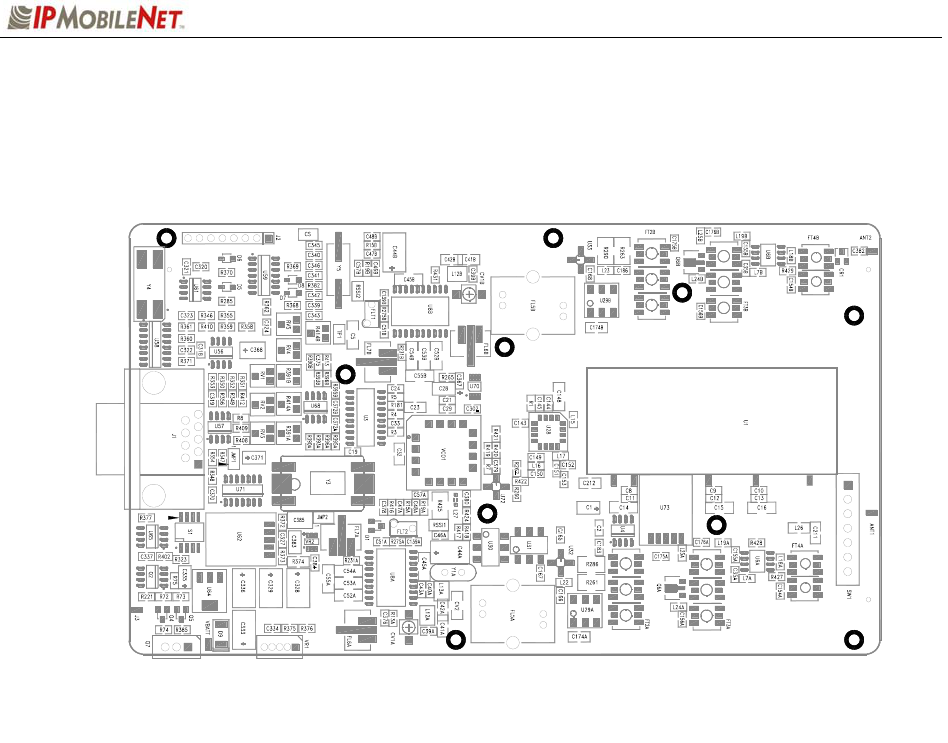
APPENDIX A: DT450 CIRCUIT BOARD DIAGRAM
~\Technical Documentation\System Manuals\FCC-Reports\DT450-FCCRpt.doc Page 17
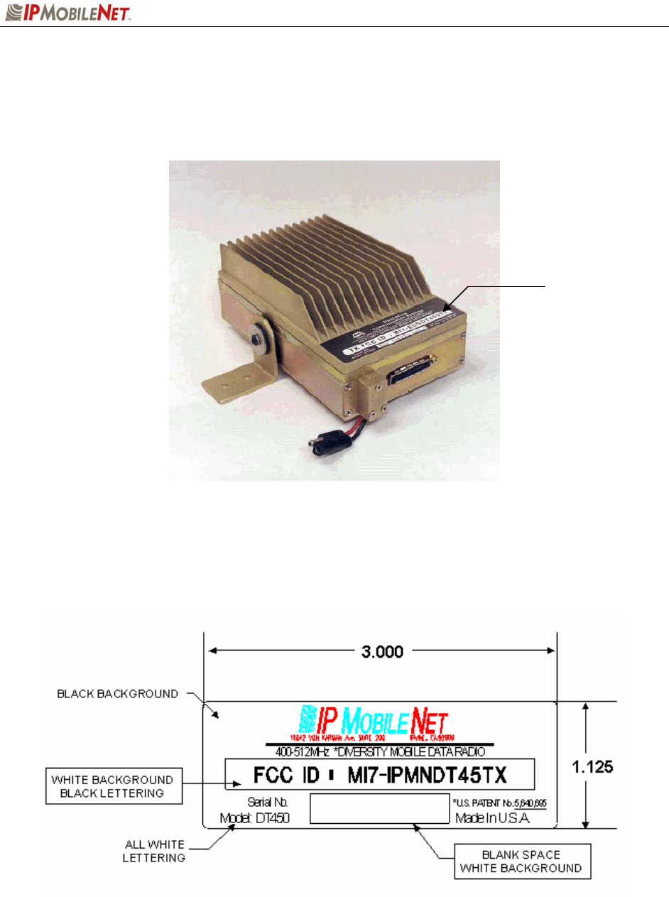
DT450 Mobile Data Radio FCC Label Placement
DT450 Mobile Data Radio FCC Label
FCC Label
Placement
SECTION 2: FACTORY TEST PROCEDURE
~\Technical Documentation\System Manuals\FCC-Reports\DT450-FCCRpt.doc Page 18