IP Mobilenet IPMNIP1B Base Station, IP1B User Manual IP1B FCCRpt
IP Mobilenet, LLC Base Station, IP1B IP1B FCCRpt
Manual

I
IN
NV
VA
AD
DR
Rt
tm
m
I
IP
P1
1B
B
B
Ba
as
se
e
S
St
ta
at
ti
io
on
n
Owner’s Manual
Date Prepared:
April 4, 2002
Document Control #: DC-27
Version: C-2 (Special Release)
Copyright 2002 IP MobileNet, Inc.
11909 East Telegraph Road Santa Fe Springs, CA 90670-3785
Voice: (562) 946-9493 Fax: (562) 949-0223

TABLE OF CONTENTS
~\Technical Documentation\System Manuals\FCC-Reports\IP1B-FCCRpt.doc Page 2
SECTION 1: THEORY OF OPERATION .................................................................................. 3
General Block Diagram ........................................................................................................... 3
System Control Block Diagram ...................................................................................... 4
Microcontroller Description................................................................................. 4
Message Processing .......................................................................................... 4
Synthesizers....................................................................................................... 5
4-Level FSK Modem Section.............................................................................. 5
Carrier Detect ..................................................................................................... 6
Host Interface ..................................................................................................... 6
Time-Out-Timer .................................................................................................. 6
Font Panel Indicators ......................................................................................... 6
Receiver Injection............................................................................................... 6
VHF Receiver ..................................................................................................... 7
VHF Front-End Section ...................................................................................... 7
45 MHz Receiver Section................................................................................... 8
Diversity Reception Controller........................................................................................ 9
Principle of Operation......................................................................................... 9
Receive Baseband Processing .......................................................................... 9
Exciter .......................................................................................................................... 10
Transmit Baseband Processing ....................................................................... 10
Exciter RF Section............................................................................................ 11
Power Amplifier Module ................................................................................... 11
SECTION 2: FCC LABEL ....................................................................................................... 12
SECTION 1: THEORY OF OPERATION
~\Technical Documentation\System Manuals\FCC-Reports\IP1B-FCCRpt.doc Page 3
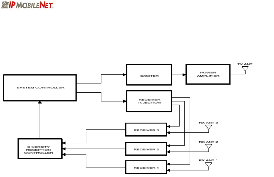
General Block Diagram
General block diagram of the IP1B, which is comprised of eight (8) PCBs (Printed Circuit Boards).
System Controller Consists of a system microcontroller, radio modem, and provides serial
communication interfaces.
DRC (Diversity Continuously selects the receiver with the best signal level to supply recovered
Reception Controller) modulation. Eliminates destructive effects of multi-path fading.
Receiver Injection Creates injection signals used by the three (3) VHF (very high frequency)
receivers to down-convert the carrier to an IF (intermediate frequency).
VHF Receiver Provides reception and demodulation of FM (frequency modulated) VHF RF
(radio frequency) signals. The receivers also provide RF carrier amplitude
information used by the DRC.
VHF Exciter Generates transmit carrier signals and performs frequency modulation.
Power Amplifier Amplifies low-level exciter RF carrier signals to the final output power level.
SECTION 1: THEORY OF OPERATION
~\Technical Documentation\System Manuals\FCC-Reports\IP1B-FCCRpt.doc Page 4
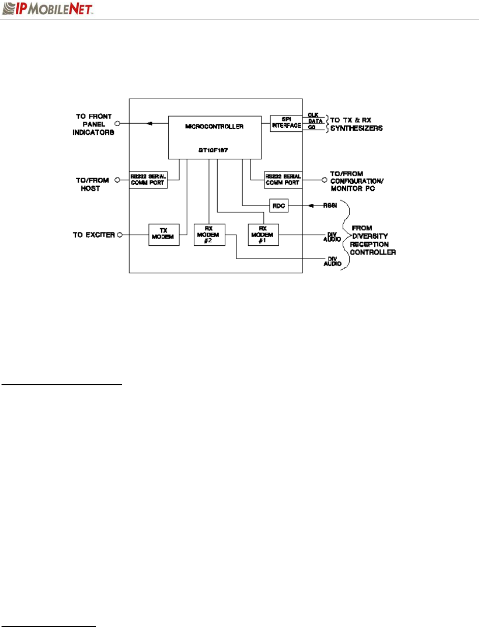
System Controller Block Diagram
Functional block diagram of the System Controller.
The system controller controls all programmable devices in the radio and handles internal and external
communications.
Microcontroller Description
The base station uses a SGS/Thomson ST10F167 microcontroller. It is a highly integrated processor
with many on chip peripherals including:
• 128K bytes of on chip Flash EPROM for program storage
• 4K bytes RAM
• UART (asynchronous serial interface)
• Synchronous serial interface
• Analog-to-digital converter
• General purpose timers
• Watchdog timer
• Reset generator
• Programmable chip selects
• Clock multiplier
• General purpose I/O pins
In addition to the microcontroller on chip memory, there are also 512K bytes of RAM for data buffers and
system use, and 2K bytes of non-volatile memory for configuration information.
Message Processing
For down-link data transmissions, the microcontroller receives data from the serial port, determines the
start and end of data frames, formats the data for transmission, turns on the transmitter, and passes the
data to the transmit modem chip. At the end of the transmission, if no other messages are ready, the
microcontroller turns off the transmitter.
SECTION 1: THEORY OF OPERATION
~\Technical Documentation\System Manuals\FCC-Reports\IP1B-FCCRpt.doc Page 5
For up-link transmissions, the microcontroller receives data from the receive modem chip, checks for
errors, adds framing and optionally signal strength information, and sends it out the serial port.
Synthesizers
The microcontroller is responsible for keeping the base station on channel by programming the digital
PLL (phase-locked-loop) frequency synthesizers. This task is accomplished via a serial communications
interface consisting of three signals PLLDATA, PLLCLOCK, and PLLENABLE. The PLLDATA signal
provides the PLL data for the synthesizer, the PLLCLOCK signal clocks the data into the synthesizer, and
the PLLENABLE signal enables synthesizer programming. After initially programming the synthesizer,
the microcontroller monitors the synthesizer's lock detect signal. Upon detecting an unlocked condition,
the microcontroller will re-program the synthesizer to lock the base station.
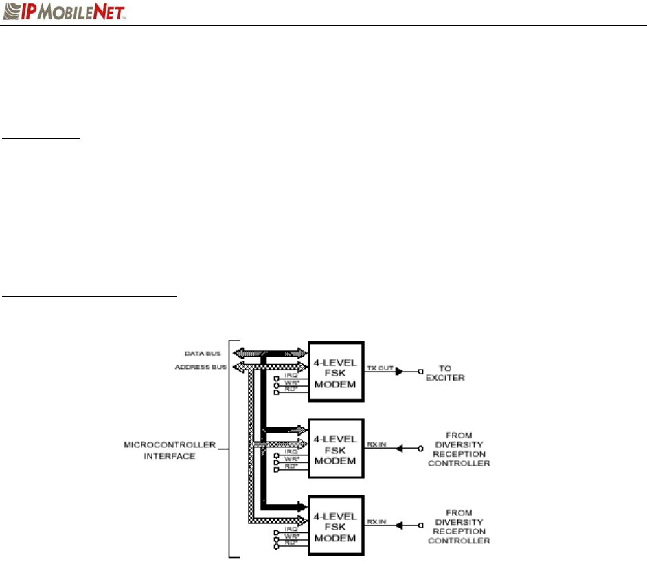
4-Level FSK Modem Section
The system controller contains two (2) internal 4-Level FSK modems for receiving and one (1) for
transmitting for reliable, high-speed transfer of data over-the-air. The modems interface with the
microcontroller and the base station’s modulation / demodulation circuits to deliver reliable two-way
transfer of high-speed application data over a wireless link.
The modem assembles application data received from the microcontroller, adds FEC (forward error
correction) and error detection (CRC - cyclic redundancy check) information and interleaves the result for
burst-error protection. After automatically adding symbol and frame sync code words, the data packet is
converted into filtered 4-Level analog signals for modulating the base station’s transmitter.
In the receive mode, the modems perform the reverse function using the analog signals from the
receivers discriminators. After error correction and removal of packet overhead, the recovered application
data is supplied to the microcontroller. CRC detected residual errors will be flagged.
The modems use data block sizes and FEC/CRC suitable for high-speed transfer of data over narrow-
band radio links. The modem can be operated at 4.8 kbps, 9.6 kbps, and 19.2 kbps under software
control. The modem IC is a highly integrated device incorporating many advanced features.
SECTION 1: THEORY OF OPERATION
~\Technical Documentation\System Manuals\FCC-Reports\IP1B-FCCRpt.doc Page 6
Carrier Detect
The base station uses RSSI (received signal strength indicator) and software to generate a carrier detect
signal. Every millisecond, the microcontroller samples RSSI through an analog-to-digital converter. If the
microcontroller detects a step increase in the RSSI voltage (greater or equal to the RSSI step threshold
setting), a carrier detect signal is generated. This carrier detect signal is used to instruct the 4-level FSK
modems to search for an incoming data message.
Host Interface
The host interface is an RS232 serial port. The base station is a DTE (data terminal equipment) device.
Typically, only TXD, RXD and GROUND are used to connect to the host. The control signals are
available if required for a particular application. The recommended serial port settings are 19200 baud,
no parity, eight (8) data bits, and one (1) stop bit. These settings are user programmable.
The type of framing used on the host interface is configurable. It supports either RIM framing or SLIP
framing. RIM framing is the format used by previous generation IPMobileNet base stations.
The base station can also be used with an external modulation source. This is used when upgrading
existing IPMobileNet systems.
In addition to the host serial port, there is an INVADR Base Station I/O Board that is used for configuring
and monitoring the base station. A computer running a terminal emulation program can be connected to
this port. Its settings are 9600 baud, no parity, eight (8) data bits, and one (1) stop bit. The I/O board
also has additional connections used for testing purposes.
Time-Out-Timer
The microcontroller provides a programmable transmit time-out-timer function to eliminate the possibility
of inadvertent continuous transmit operation.
Front Panel Indicators
The microcontroller is responsible for controlling the illumination of the front panel indicators.
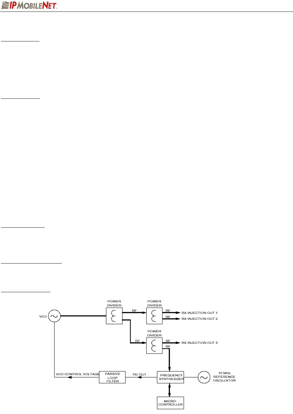
Receiver Injection
Functional block diagram of the receiver injection.
SECTION 1: THEORY OF OPERATION
~\Technical Documentation\System Manuals\FCC-Reports\IP1B-FCCRpt.doc Page 7
The receiver injection synthesizer creates the injection signals used by the three (3) internal FM receivers.
The receiver injection frequency is 45 MHz below the base station’s receive frequency.
The VHF signal from the VCO is applied to amplifier for amplification and load isolation and is then routed
to a 4-way divider network. The divider network splits the injection signal into four (4) equal amplitude
signals. Three (3) of these signals are used as injection signals for the three (3) receivers; the fourth
signal is sent back to the synthesizer as feedback for the PLL.
The feedback signal is used by the digital frequency synthesizer to keep the radio on channel.
The frequency synthesizer divides the injection signal to produce a quotient signal of 12.5 kHz . The
synthesizer also divides the signal from the 10.0 MHz reference oscillator to produce a 12.5 kHz signal.
The synthesizer compares the phase of these two (2) signals and outputs a signal (PD OUT) proportional
to their phase difference. A passive loop filter converts the PD OUT signal to a DC control voltage that
locks the VCO on channel.
In this manner, the VCO is compared to - and forced to emulate - the high-stability reference oscillator.
This configuration is commonly referred to as a digital Phase-Locked-Loop (PLL) frequency synthesizer.
VHF Receiver
The IP1B employs three (3) independent, high-performance, low-noise, dual conversion FM receivers.
The receiver is divided into two (2) main sections, a front-end section and a 45 MHz receiver section.
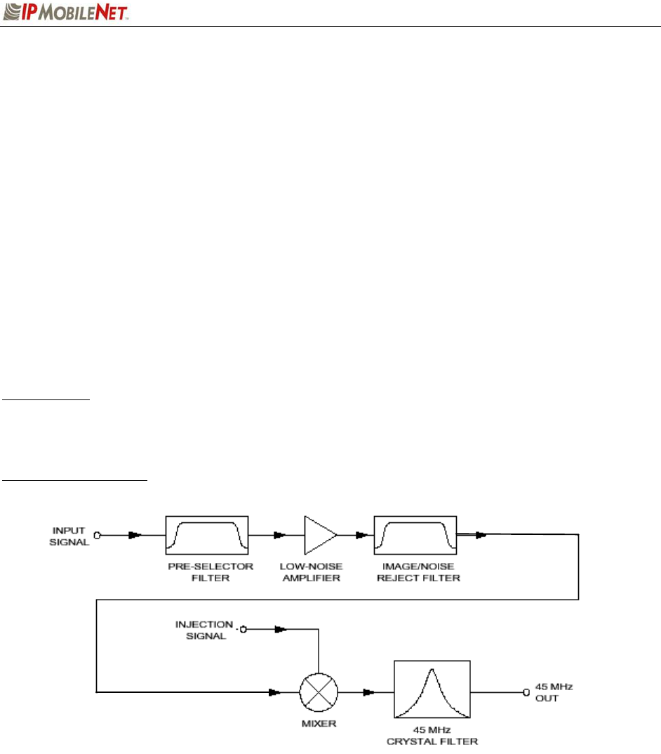
VHF Front-End Section
Functional block diagram of the receiver front-end section.
The front-end section employs an advanced-architecture, cascaded-LNA (low noise amplifier) design for
extreme sensitivity and high-overload performance.
Receiver input signals are first filtered by a pre-selector band-pass filter and are then routed to a LNA.
The amplified signal is routed through another band-pass filter.
SECTION 1: THEORY OF OPERATION
~\Technical Documentation\System Manuals\FCC-Reports\IP1B-FCCRpt.doc Page 8
After the final band-pass filter, the signal is applied to a mixer where it is mixed with the receiver injection
signal (45 MHz below the received signal) to produce a first IF of 45 MHz. The 45 MHz IF is passed by a
45 MHz crystal filter and is routed to the 45 MHz receiver section for further processing.
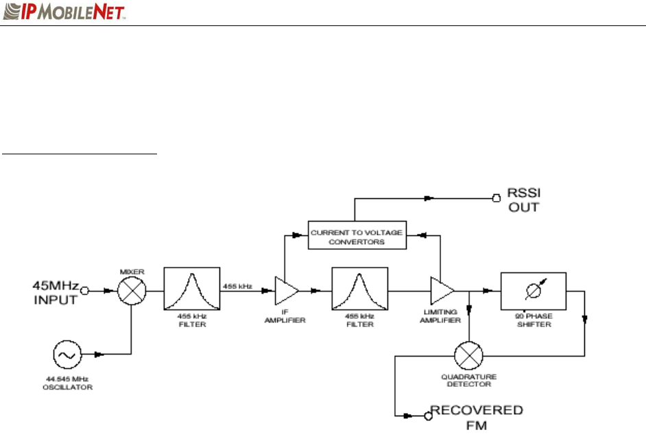
45 MHz Receiver Section
Functional block diagram of the 45 MHz receiver.
The 45 MHz IF from the front-end is mixed with a 44.545 MHz injection frequency to produce a 455 kHz
second IF which is passed by a 455 kHz filter. This second IF is then amplified and limited by an IF
amplifier and limiting amplifier respectively. A 455 kHz filter provides interstage filtering between the IF
amplifier and the IF limiting amplifier.
This section includes the current-to-voltage converters, which produce the RSSI signal (a DC voltage
proportional to the log of the received signal strength). The RSSI responds to signals as low as -125 dBm
and rises monotonically over a range of approximately 90 dB. RSSI is used by the DRC to select the best
receiver at any particular point in time.
The output of the limiting amplifier is applied to a tuned quadrature detector, which outputs recovered FM.
SECTION 1: THEORY OF OPERATION
~\Technical Documentation\System Manuals\FCC-Reports\IP1B-FCCRpt.doc Page 9
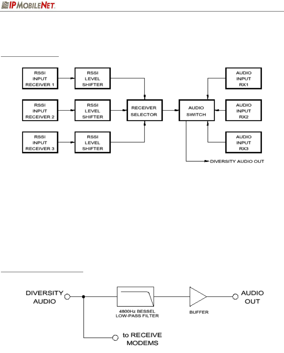
Diversity Reception Controller
Principle of Operation
The DRC is the central processor of a patented triple-receiver DRC.
The DRC accepts inputs from three (3) receivers, determines which receiver has the best SNR (signal-to-
noise ratio), and selects that receiver to supply recovered modulation.
High-speed RSSI from the three (3) receivers are processed by the RSSI input and RSSI level- shifter
sections, and are then forwarded to the receiver selector. The receiver selector selects the appropriate
receiver.
Audio from each receiver is processed by the audio input section and is sent to the audio switch. The
audio switch performs the actual selection process as directed by the receiver selector.
Receive Baseband Processing
Functional diagram of the receive baseband processing section.
DIVAUDIO (diversity audio) from the DRC is routed to two (2) separate paths, depending on whether the
audio is destined for an external device (control head, eternal modem, etc.) or for the internal 4-level FSK
modems.
SECTION 1: THEORY OF OPERATION
~\Technical Documentation\System Manuals\FCC-Reports\IP1B-FCCRpt.doc Page 10
DIVAUDIO is routed directly to the internal modem as the modem provides internal filtering of received
signals.
For an external device, DIVAUDIO is routed through a 4800 Hz eighth-order Bessel low-pass filter. The
purpose of the filter is to improve the SNR of the recovered signal. Following the filter, the signal is
buffered to provide load isolation and is routed to an external device as FDATA (filtered, diversity
recovered modulation).
Exciter
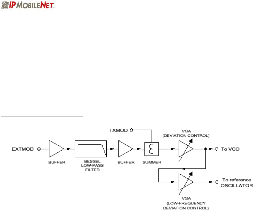
Transmit Baseband Processing
Functional diagram of the IP1B’s transmit baseband processing section.
The IP1B is capable of being modulated by an external device (console, external modem, etc.) or by the
internal 4-level FSK modem. External modulation and internal modem modulation are, at any point in
time, mutually exclusive.
EXTMOD (external modulation) from an external device is buffered to provide load isolation and is then
routed to an eighth-order Bessel low-pass filter. The purpose of this filter is to remove any high-frequency
components present in the external modulation prior to application to the transmit modulator. Following
the filter, the external modulation is buffered to provide load isolation to the filter. The modulation is
routed though a summer and is applied to a VGA (variable gain amplifier) which provides transmit
modulation deviation control.
The output of the first VGA directly modulates the VCO. This signal is also routed through another VGA,
which provides low-frequency deviation control by modulating the reference oscillator. This configuration
is referred to as two-point modulation (with the VCO and the reference oscillator being the two (2)
modulation points). Two-point modulation prevents the radio's PLL circuitry from counteracting the
modulation process, and provides a clean flat modulation response to the low frequency portion of the
baseband spectrum.
4-level FSK modulation from the internal modem bypasses the Bessel filter as the modem contains built-
in filtering. This modulation is routed through the summer and is similarly sent to the VCO and reference
oscillator in the same manner as the external modulation.
SECTION 1: THEORY OF OPERATION
~\Technical Documentation\System Manuals\FCC-Reports\IP1B-FCCRpt.doc Page 11
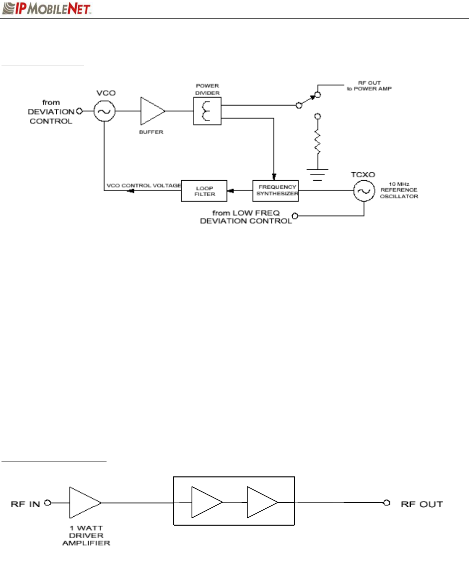
Exciter RF Section
Functional block diagram of the exciter RF section.
The exciter RF section generates the transmit RF carrier and accomplishes FM modulation. The VHF
signal from the VCO is applied to a buffer and is then routed to a divider network. The divider network
splits the RF signal into two (2) equal amplitude signals. One of these signals is used as the exciter
output; the other is sent back to the synthesizer as feedback for the PLL.
The frequency synthesizer divides the VHF signal to produce a quotient signal of 12.5 kHz. The
synthesizer also divides the signal from the 10.0 MHz reference oscillator to produce a 12.5 kHz signal.
The synthesizer compares the phase of these two (2) signals and outputs a signal (PD OUT) proportional
to their phase difference. A passive loop filter converts the PD OUT signal to a DC control voltage, which
locks the VCO on channel.
In this manner, the VCO is compared to - and forced to emulate - the high-stability reference oscillator.
This configuration is commonly referred to as a digital Phase-Locked-Loop (PLL) frequency synthesizer.
Power Amplifier Module
Functional diagram of the power amplifier.
The transmit injection signal from the RF injection section is applied to a one (1) watt amplifier. The
signal is then routed to the final power amplifier boosting the output signal to 60 Watts.
60 WATT
POWER AMPLIFIER
MODULE

SECTION 2: FCC LABEL
~\Technical Documentation\System Manuals\FCC-Reports\IP1B-FCCRpt.doc Page 12
FCC Label
The following table identifies the information related to FCC label placement for the IP1B.
NO. DOCUMENT
NO. DESCRIPTION
1 IP1B-Drawing INVADR IP1B Base Station Drawing – FCC Label Placement
(1 Page)
SECTION 2: FCC LABEL
~\Technical Documentation\System Manuals\FCC-Reports\IP1B-FCCRpt.doc Page 13
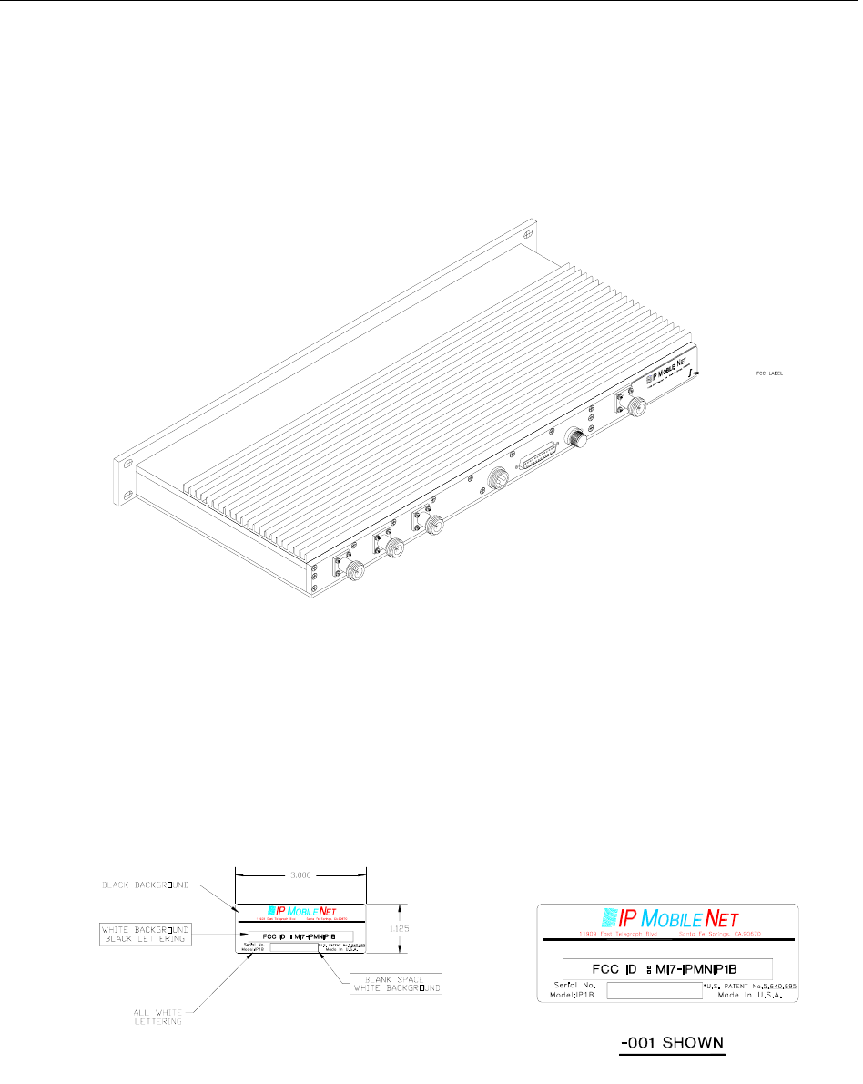
IP1B Base Station FCC Label Placement
IP1B Base Station FCC Label
ΣΧΑΛΕ : 2Ξ
ςΗΦ (150−156ΜΗζ) ΒΑΣΕ ΣΤΑΤΙΟΝ
∗∆ΙςΕΡΣΙΤΨ ΡΕΧΕΠΤΙΟΝ ΣΨΣΤΕΜ
ςΗΦ (150−156ΜΗζ) ΒΑΣΕ ΣΤΑΤΙΟΝ
∗∆Ις ΕΡΣΙΤΨ ΡΕΧΕΠΤΙΟΝ ΣΨΣΤΕΜ