IP Mobilenet IPMNIP4 HPV/GPS Mobile Radio User Manual MX919BDB r3
IP Mobilenet, LLC HPV/GPS Mobile Radio MX919BDB r3
Contents
- 1. Manual
- 2. Information
Information
COMMUNICATION SEMICONDUCTORS
MX919B
DATA BULLETIN 4-Level FSK Modem Data Pump
©2001 MX•COM, INC. www.mxcom.com Tele: 800 638 5577 336 744 5050 Fax: 336 744 5054 Doc. # 20480170.003
4800 Bethania Station Road, Winston-Salem, NC 27105-1201 USA All trademarks and service marks are held by their respective companies.
PRELIMINARY INFORMATION
Features Applications
• 4-Level Root Raised Cosine FSK Modulation
• Half Duplex, 4800 to 19.2kbps
• Increase Channel Bit Rate/Hz
• Full Data Packet Framing
• Impulse and NRZ Signal Modes
• Enhanced Performance in Noisy Conditions
• Error Detection and Error Correction
• Low Power 3.3V/5.0V Operation
• Wireless Data Terminals
• Two Way Paging Systems
• Digital Radio Systems
• Wide Area Wireless Data Broadcasts
• Point to Point Wireless Data Links
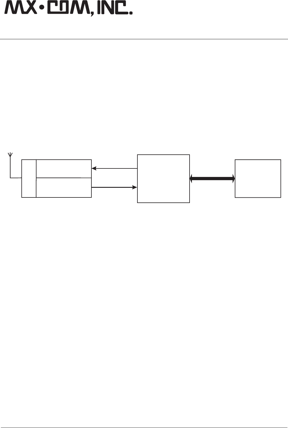
MODEM
DATA
PUMP
MX919B
ANALOG TX DATA AND
CONTROL BUS
ANALOG RX
RF
RADIO
DISCRIMINATOR
MODULATOR SYSTEM
APPLICATION
PROCESSING
HOST Cµ
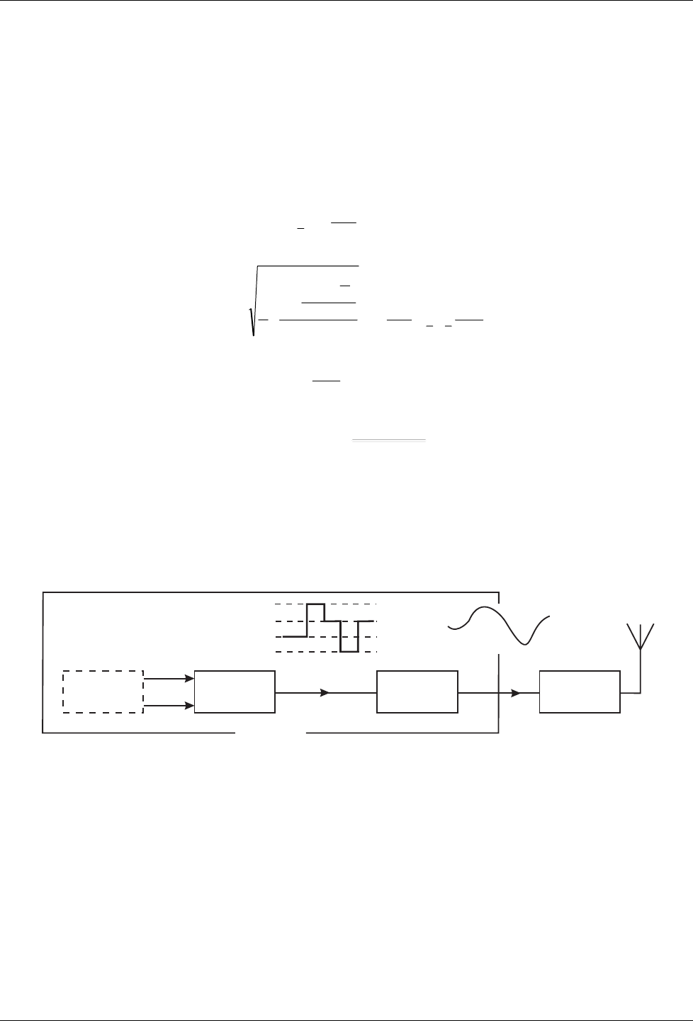
The MX919B is a low voltage CMOS device containing all of the baseband signal processing and Medium
Access Control (MAC) protocol functions required for a high performance 4-level FSK Wireless Packet Data
Modem. It interfaces with the modem host µC and the radio modulation/demodulation circuits to deliver
reliable two-way transfer of the application data over a wireless link.
The MX919B assembles application data received from the host µC, adds forward error correction (FEC) and
error detection (CRC) information, and interleaves the result for burst-error protection. After automatically
adding symbol and frame sync codewords, the data packet is converted into filtered 4-level analog signals for
modulating the radio transmitter.
In receive mode, the MX919B performs the reverse function using the analog signals from the receiver
discriminator. After error correction and removal of the packet overhead, the recovered application data is
supplied to the host µC. CRC detected residual uncorrected data errors will be flagged. A readout of the
SNR value during receipt of a packet is also provided.
The MX919B uses data block sizes and FEC/CRC suitable for applications where high-speed transfer of data
over narrow-band wireless links is required. The device is programmable to operate at standard bit rates from
a wide range of Xtal/clock frequencies.
The MX919B may be used with a 3.0V to 5.5V power supply and is available in the following package styles:
24-pin SSOP (MX919BDS), 24-pin SOIC (MX919BDW), 24-pin PLCC (MX919BLH), and 24-pin PDIP
(MX919BP).

4-Level FSK Modem Data Pump Page 2 of 47 MX919B PRELIMINARY INFORMATION
©2001 MX•COM, INC. www.mxcom.com Tele: 800 638 5577 336 744 5050 Fax: 336 744 5054 Doc. # 20480170.003
4800 Bethania Station Road, Winston-Salem, NC 27105-1201 USA All trademarks and service marks are held by their respective companies.
CONTENTS
Section Page
1. Block Diagram ............................................................................................................... 6
2. Signal List...................................................................................................................... 7
3. External Components ................................................................................................... 8
4. General Description ...................................................................................................... 9
4.1 Description of Blocks ......................................................................................................... 9
4.1.1 Data Bus Buffers..................................................................................................................... 9
4.1.2 Address and R/W Decode ...................................................................................................... 9
4.1.3 Status and Data Quality Registers.......................................................................................... 9
4.1.4 Command, Mode, and Control Registers ............................................................................... 9
4.1.5 Data Buffer.............................................................................................................................. 9
4.1.6 CRC Generator/Checker ........................................................................................................ 9
4.1.7 FEC Generator/Checker ......................................................................................................... 9
4.1.8 Interleave/De-Interleave Buffer............................................................................................... 9
4.1.9 Frame Sync Detect ................................................................................................................. 9
4.1.10 Rx Input Amp ........................................................................................................................ 10
4.1.11 RRC Low Pass Filter ............................................................................................................ 10
4.1.12 Tx Output Buffer.................................................................................................................... 11
4.1.13 Rx Level/Clock Extraction..................................................................................................... 12
4.1.14 Clock Oscillator and Dividers................................................................................................ 12
4.2 Modem - µC Interaction ................................................................................................... 12
4.3 Binary to Symbol Translation ........................................................................................... 13
4.4 Frame Structure............................................................................................................... 14
4.5 The Programmer’s View................................................................................................... 15
4.5.1 Data Block Buffer .................................................................................................................. 15
4.5.2 Command Register............................................................................................................... 15
4.5.2.1 Command Register B7: AQSC - Acquire Symbol Clock ................................................ 16
4.5.2.2 Command Register B6: AQLEV - Acquire Receive Signal Levels ................................. 16
4.5.2.3 Command Register B5: CRC ........................................................................................ 16
4.5.2.4 Command Register B4: TXIMP - Tx Level/Impulse Shape ............................................ 16
4.5.2.5 Command Register B3 - Reserved ................................................................................ 16
4.5.2.6 Command Register B2, B1, B0: TASK........................................................................... 16
4.5.2.7 NULL: No effect .............................................................................................................. 18
4.5.2.8 SFSH: Search for Frame Sync plus Header Block ........................................................ 18
4.5.2.9 RHB: Read Header Block............................................................................................... 18
4.5.2.10 RILB: Read 'Intermediate' or 'Last' Block ....................................................................... 18
4.5.2.11 SFS: Search for Frame Sync ......................................................................................... 18
4.5.2.12 R4S: Read 4 Symbols .................................................................................................... 19
4.5.2.13 T24S: Transmit 24 Symbols ........................................................................................... 19
4.5.2.14 THB: Transmit Header Block.......................................................................................... 19
4.5.2.15 TIB: Transmit Intermediate Block ................................................................................... 20
4.5.2.16 TLB: Transmit Last Block ............................................................................................... 20

4-Level FSK Modem Data Pump Page 3 of 47 MX919B PRELIMINARY INFORMATION
©2001 MX•COM, INC. www.mxcom.com Tele: 800 638 5577 336 744 5050 Fax: 336 744 5054 Doc. # 20480170.003
4800 Bethania Station Road, Winston-Salem, NC 27105-1201 USA All trademarks and service marks are held by their respective companies.
4.5.2.17 T4S: Transmit 4 Symbols ............................................................................................... 20
4.5.2.18 RESET: Stop any current action .................................................................................... 20
4.5.2.19 Task Timing .................................................................................................................... 20
4.5.2.20 RRC Filter Delay............................................................................................................. 21
4.5.3 Control Register .................................................................................................................... 22
4.5.3.1 Control Register B7, B6: CKDIV - Clock Division Ratio ................................................. 22
4.5.3.2 Control Register B5, B4: FSTOL - Frame Sync Tolerance to Inexact Matches............. 22
4.5.3.3 Control Register B3, B2: LEVRES - Level Measurement Modes .................................. 23
4.5.3.4 Control Register B1, B0: PLLBW - Phase-Locked Loop Bandwidth Modes .................. 23
4.5.4 Mode Register....................................................................................................................... 24
4.5.4.1 Mode Register B7: IRQEN - IRQ Output Enable ......................................................... 24
4.5.4.2 Mode Register B6: INVSYM - Invert Symbols................................................................ 24
4.5.4.3 Mode Register B5: RXTX/ - Tx/Rx Mode ...................................................................... 24
4.5.4.4 Mode Register B4: RXEYE - Show Rx Eye.................................................................... 25
4.5.4.5 Mode Register B3: PSAVE - Powersave........................................................................ 25
4.5.4.6 Mode Register B2, B1, B0.............................................................................................. 25
4.5.5 Status Register ..................................................................................................................... 26
4.5.5.1 Status Register B7: IRQ - Interrupt Request .................................................................. 26
4.5.5.2 Status Register B6: BFREE - Data Block Buffer Free.................................................... 26
4.5.5.3 Status Register B5: IBEMPTY - Interleave Buffer Empty............................................... 26
4.5.5.4 Status Register B4: DIBOVF - De-Interleave Buffer Overflow ....................................... 26
4.5.5.5 Status Register B3: CRCERR - CRC Checksum Error.................................................. 27
4.5.5.6 Status Register B2, B1, B0............................................................................................. 27
4.5.6 Data Quality Register............................................................................................................ 27
4.6 CRC, FEC, and Interleaving............................................................................................. 27
4.6.1 Cyclic Redundancy Codes.................................................................................................... 27
4.6.1.1 CRC1 .............................................................................................................................. 27
4.6.1.2 CRC2 .............................................................................................................................. 28
4.6.1.3 Forward Error Correction................................................................................................ 28
4.6.1.4 Interleaving ..................................................................................................................... 28
4.7 Transmitted Symbol Shape.............................................................................................. 28
5. Application................................................................................................................... 30
5.1 Transmit Frame Example................................................................................................. 30
5.2 Receive Frame Example.................................................................................................. 33
5.3 Clock Extraction and Level Measurement Systems.......................................................... 36
5.3.1 Supported Types of Systems................................................................................................ 36
5.3.2 Clock and Level Acquisition Procedures with RF Carrier Detect ......................................... 36
5.3.3 Clock and Level Acquisition Procedure without RF Carrier Detect ...................................... 36
5.3.4 Automatic Acquisition Functions........................................................................................... 37
5.4 AC Coupling.....................................................................................................................37
5.5 Radio Performance.......................................................................................................... 39
5.6 Received Signal Quality Monitor ...................................................................................... 40

4-Level FSK Modem Data Pump Page 4 of 47 MX919B PRELIMINARY INFORMATION
©2001 MX•COM, INC. www.mxcom.com Tele: 800 638 5577 336 744 5050 Fax: 336 744 5054 Doc. # 20480170.003
4800 Bethania Station Road, Winston-Salem, NC 27105-1201 USA All trademarks and service marks are held by their respective companies.
6. Performance Specification......................................................................................... 41
6.1 Electrical Performance..................................................................................................... 41
6.1.1 Absolute Maximum Ratings .................................................................................................. 41
6.1.2 Operating Limits.................................................................................................................... 41
6.1.3 Operating Characteristics ..................................................................................................... 42
6.1.3.1 Operating Characteristics Notes: ................................................................................... 42
6.1.4 Timing ................................................................................................................................... 43
6.1.5 Typical Bit Error Rate............................................................................................................ 45
6.2 Packaging........................................................................................................................ 46
MX-COM, Inc. Reserves the right to change specifications at any time and without notice

4-Level FSK Modem Data Pump Page 5 of 47 MX919B PRELIMINARY INFORMATION
©2001 MX•COM, INC. www.mxcom.com Tele: 800 638 5577 336 744 5050 Fax: 336 744 5054 Doc. # 20480170.003
4800 Bethania Station Road, Winston-Salem, NC 27105-1201 USA All trademarks and service marks are held by their respective companies.
Figures
Figure Page
Figure 1: Block Diagram ..................................................................................................................................... 6
Figure 2: Recommended External Components ................................................................................................ 8
Figure 3: Typical Modem µC connections .......................................................................................................... 9
Figure 4: Translation of Binary Data to Filtered 4-Level Symbols in Tx Mode................................................. 10
Figure 5: RRC Filter Frequency Response vs. Bit Rate (including the external RC filter R4/C5).................... 11
Figure 6: RRC Filter Frequency Response vs. Symbol Rate (including the external RC filter R4/C5)............ 11
Figure 7: Over-Air Signal Format ..................................................................................................................... 14
Figure 8: Alternative Frame Structures ............................................................................................................ 15
Figure 9: Transmit Task Overlapping ............................................................................................................... 17
Figure 10: Receive Task Overlapping .............................................................................................................. 17
Figure 11: Transmit Task Timing Diagram ....................................................................................................... 21
Figure 12: Receive Task Timing Diagram ........................................................................................................ 21
Figure 13: RRC Low Pass Filter Delay............................................................................................................. 21
Figure 14: Ideal 'RXEYE' Signal....................................................................................................................... 25
Figure 15: Typical Data Quality Reading vs S/N.............................................................................................. 27
Figure 16: Input Signal to RRC Filter in Tx Mode for TXIMP = 0 and 1...........................................................28
Figure 17: Tx Signal Eye TXIMP = 0................................................................................................................ 29
Figure 18: Tx Signal Eye TXIMP = 1................................................................................................................ 29
Figure 19: Transmit Frame Example Flowchart, Main Program ......................................................................31
Figure 20: Tx Interrupt Service Routine ........................................................................................................... 32
Figure 21: Receive Frame Example Flowchart, Main Program ........................................................................34
Figure 22: Rx Interrupt Service routine ............................................................................................................ 35
Figure 23: Acquisition Sequence Timing.......................................................................................................... 36
Figure 24: Effect of AC Coupling on BER (without FEC) ................................................................................. 37
Figure 25: Decay Time - AC Coupling.............................................................................................................. 38
Figure 26: Typical Connections between Radio and MX919B......................................................................... 39
Figure 27: Received Signal Quality Monitor Flowchart .................................................................................... 40
Figure 28: µC Parallel Interface Timings.......................................................................................................... 44
Figure 29: Typical Bit Error Rate With and Without FEC ................................................................................. 45
Figure 30: 24-pin SOIC Mechanical Outline: Order as part no. MX919BDW ................................................. 46
Figure 31: 24-pin SSOP Mechanical Outline: Order as part no. MX919BDS ................................................. 46
Figure 32: 24-pin PLCC Mechanical Outline : Order as part no. MX919BLH ................................................. 47
Figure 33: 24-pin PDIP Mechanical Outline: Order as part no. MX919BP ..................................................... 47
4-Level FSK Modem Data Pump Page 6 of 47 MX919B PRELIMINARY INFORMATION
©2001 MX•COM, INC. www.mxcom.com Tele: 800 638 5577 336 744 5050 Fax: 336 744 5054 Doc. # 20480170.003
4800 Bethania Station Road, Winston-Salem, NC 27105-1201 USA All trademarks and service marks are held by their respective companies.
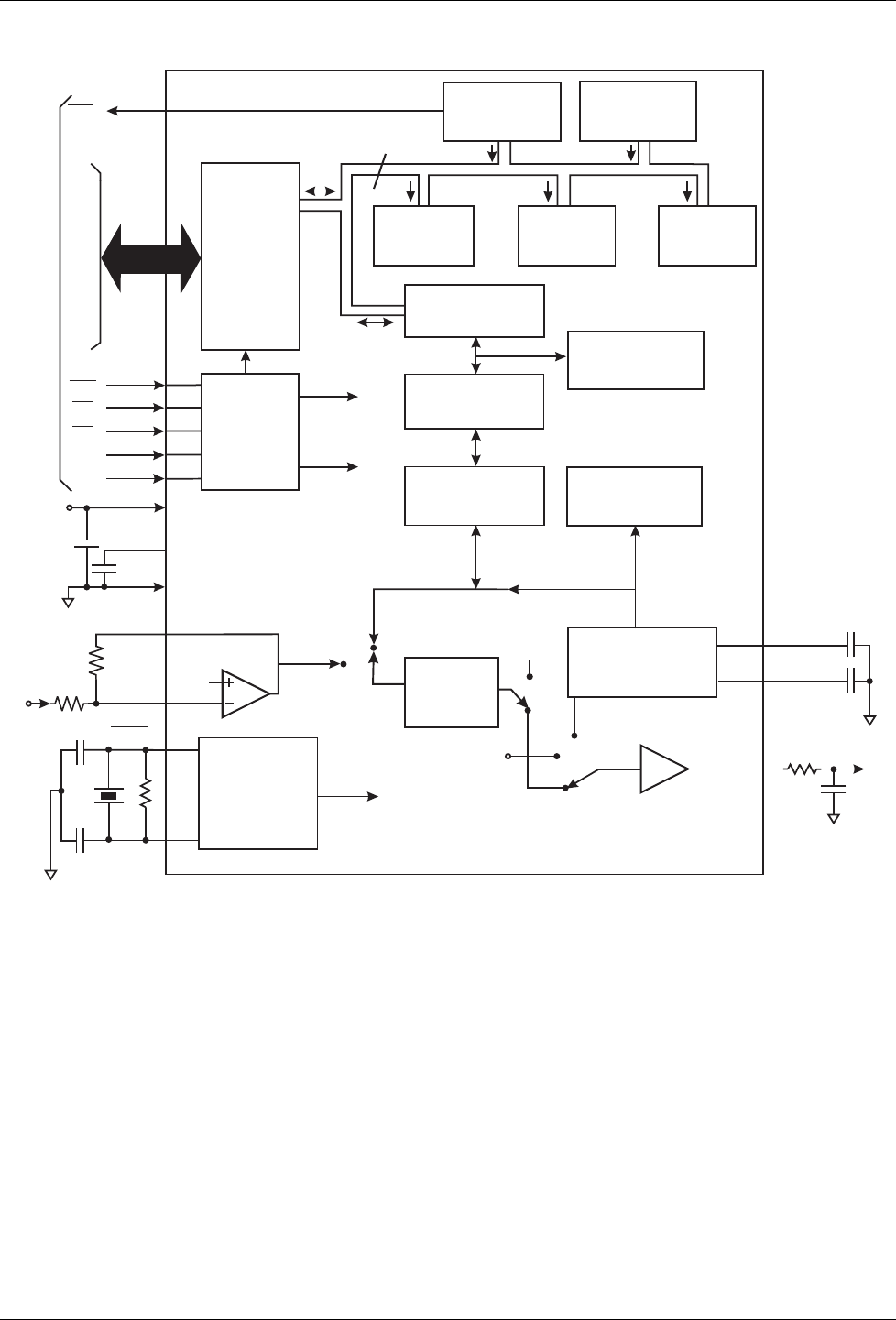
1. Block Diagram
VSS
VBIAS
XTAL /
CLOCK
TXOUT
RXIN
Rx Input Amp
Tx Output Buffer
DOC1
DOC2
D0
D1
D2
D3
D4
D5
D6
D7
A0
A1
8
Tx
Tx Symbols Rx Symbols
Tx
Rx
Tx
Rx
RxEye
VBIAS
µCONTROLLER
INTERFACE
DATA
BUS
BUFFERS
ADDRESS
AND
R/W
DECODE
CRC
GENERATOR/
CHECKER
FRAME
SYNC DETECT
Rx LEVEL/CLOCK
EXTRACTION
FEC
ENCODER/
DECODER
INTERLEAVE/
DE-INTERLEAVE
CONTROL
REGISTER
MODE
REGISTER
COMMAND
REGISTER
DATA
BUFFER
STATUS
REGISTER
DATA
QUALITY
REGISTER
RRC
LOW PASS
FILTER
CLOCK
OSCILLATOR
AND
DIVIDERS
RXAMPOUT
V
DD
XTAL
WR
RD
CS
IRQ
V
DD VBIAS
Rx
Figure 1: Block Diagram

4-Level FSK Modem Data Pump Page 7 of 47 MX919B PRELIMINARY INFORMATION
©2001 MX•COM, INC. www.mxcom.com Tele: 800 638 5577 336 744 5050 Fax: 336 744 5054 Doc. # 20480170.003
4800 Bethania Station Road, Winston-Salem, NC 27105-1201 USA All trademarks and service marks are held by their respective companies.
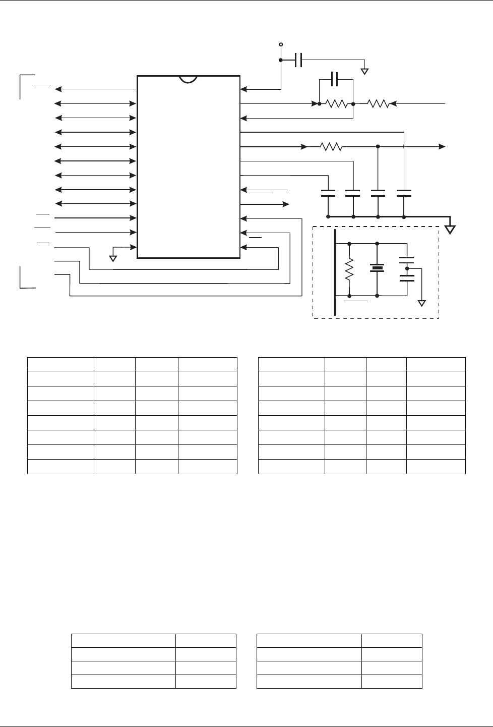
2. Signal List
Pin No. Signal Type Description
1 IRQ output A 'wire-ORable' output for connection to the host µC's Interrupt
Request input. When active, this output has a low impedance pull
down to VSS. It has high impedance when inactive.
2 D7 BUS
3 D6 BUS
4 D5 BUS
5 D4 BUS
6 D3 BUS
7 D2 BUS
8 D1 BUS
9 D0 BUS
Pins 2-9 (D7-D0) are 8-bit, bi-directional,
3-state µC interface data lines
10 RD input Read. An active low logic level input used to control the reading of data
from the modem into the host µC.
11 WR Input Write. An active low logic level input used to control the writing of data
into the modem from the host µC.
12 VSS power Negative supply (ground).
13 CS input Chip Select. An active low logic level input to the modem used to
enable a data read or write operation.
14 A0 input Logic level modem register select input
15 A1 input Logic level modem register select input
16 XTAL output Output of the on-chip oscillator.
17 XTAL/CLOCK input Input to the on-chip oscillator, for an external Xtal circuit or clock.
18 DOC2 output
Connection to the Rx level measurement circuitry. Should be
capacitive coupled to VSS .
19 DOC1 output
Connection to the Rx level measurement circuitry. Should be
capacitive coupled to VSS
20 TXOUT output Tx signal output from the modem.
21 VBIAS output
A bias line for the internal circuitry held at VDD/2. This pin must be
bypassed to VSS by a capacitor mounted close to the device pins.
22 RXIN input Input to the Rx input amplifier.
23 RXAMPOUT output Output of the Rx input amplifier.
24 VDD power
Positive supply. Levels and voltages are dependent upon this supply.
This pin should be bypassed to VSS by a capacitor mounted close to
the device pins.
Table 1: Signal List
4-Level FSK Modem Data Pump Page 8 of 47 MX919B PRELIMINARY INFORMATION
©2001 MX•COM, INC. www.mxcom.com Tele: 800 638 5577 336 744 5050 Fax: 336 744 5054 Doc. # 20480170.003
4800 Bethania Station Road, Winston-Salem, NC 27105-1201 USA All trademarks and service marks are held by their respective companies.
3. External Components
DOC1
DOC2
VDD
VDD
VSS
V
BIAS
RXIN
From Rx FM
Discriminator
To Tx Frequency
Modulator
RXAMPOUT R2
R4
R1
µCONTROLLER INTERFACE
MX919B
TXOUT
C7 C5
C3
C4
R3
X1
C6
C8
C2
D7
D6
D5
D4
D3
D2
D1
D0
A0
A1
A1
A0
XTAL/CLOCK
XTAL/CLOCK
1
2
3
4
5
6
8
9
10
11
12 13
14
7
24
23
22
21
20
19
18
17
17
16
16
15
IRQ
XTAL
XTAL
RD
WR
CS CS
C1
Figure 2: Recommended External Components
Component Notes Value Tolerance Component Notes Value Tolerance
R1 3
±20% C4 3 ±20%
R2
100kΩ ±5% C5 4 ±5%
R3
1MΩ ±20% C6 5 ±20%
R4
100kΩ ±5% C7 5 ±20%
C1 0.1µF
±20% C8 4 ±5%
C2 0.1µF
±20%
C3 3
±20% X1 2,3
Table 2: Recommended External Components
Recommended External Component Notes:
1. See Section 4.1.10.
2. For best results, a crystal oscillator design should drive the clock inverter input with signal levels of at
least 40% of VDD, peak to peak. Tuning fork crystals generally cannot meet this requirement. To obtain
crystal oscillator design assistance, consult your crystal manufacturer.
3. The values used for C3 and C4 should be suitable for the frequency of the crystal X1. As a guide, values
(including stray capacitance) of 33pF at 1MHz falling to 18pF at 10MHz will generally prove suitable.
Crystal frequency tolerances are discussed in Section 4.5.3.4.
4. Values C5 and C8 should be equal to 750,000 / symbol rate, e.g.
5. Values C6 and C7 should be equal to 50,000 / symbol rate, e.g.
Symbol Rate C5 and C8 Symbol Rate C6 and C7
2400 symbols/second 330pF 2400 symbols/second 0.022µF
4800 symbols/second 150pF 4800 symbols/second 0.01µF
9600 symbols/second 82pF 9600 symbols/second 4700pF
4-Level FSK Modem Data Pump Page 9 of 47 MX919B PRELIMINARY INFORMATION
©2001 MX•COM, INC. www.mxcom.com Tele: 800 638 5577 336 744 5050 Fax: 336 744 5054 Doc. # 20480170.003
4800 Bethania Station Road, Winston-Salem, NC 27105-1201 USA All trademarks and service marks are held by their respective companies.
4. General Description
4.1 Description of Blocks
4.1.1 Data Bus Buffers
Eight bi-directional 3-state logic level buffers between the modem's internal registers and the host µC's data
bus lines.
4.1.2 Address and R/W Decode
This block controls the transfer of data bytes between the µC and the modem's internal registers according to
the state of the Write and Read Enable inputs ( WR and RD ), the Chip Select input ( SC ), and the Register
Address inputs A0 and A1.
The Data Bus Buffers, Address, and R/W Decode blocks provide a byte-wide parallel µC interface, which can
be memory-mapped, as shown in Figure 3.
Address Bus
µCMODEM
WR
RD
CS
RD
Address Decode
Circuit
Data Bus
IRQ
VDD
D0:7
A0:1
WR
IRQ pull up
resistor
D0:7
IRQ
A2:7
A0:1
Figure 3: Typical Modem µ
µµ
µC connections
4.1.3 Status and Data Quality Registers
Two, 8-bit registers which the µC can read, to determine the status of the modem and received data quality.
4.1.4 Command, Mode, and Control Registers
The values written by the µC to these 8-bit registers control the operation of the modem.
4.1.5 Data Buffer
A 12-byte buffer used to hold receive or transmit data to or from the µC.
4.1.6 CRC Generator/Checker
A circuit which generates (in transmit mode) or checks (in receive mode) the Cyclic Redundancy Checksum
bits, which may be included in the transmitted data blocks so the receive modem can detect transmission
errors.
4.1.7 FEC Generator/Checker
In transmit mode, this circuit adds Forward Error Correction bits to the transmitted data, resulting in the
conversion of binary data to 4-level symbols. In receive mode, this circuit translates received 4-level symbols
to binary data, using the FEC information to correct a large proportion of transmission errors.
4.1.8 Interleave/De-Interleave Buffer
This circuit interleaves data symbols within a block before transmission and de-interleaves the received data
so that the FEC system is best able to handle short noise bursts or fades.
4.1.9 Frame Sync Detect
This circuit, which is only active in receive mode, is used to look for the 24-symbol Frame Synchronization
pattern that is transmitted to mark the start of every frame.
4-Level FSK Modem Data Pump Page 10 of 47 MX919B PRELIMINARY INFORMATION
©2001 MX•COM, INC. www.mxcom.com Tele: 800 638 5577 336 744 5050 Fax: 336 744 5054 Doc. # 20480170.003
4800 Bethania Station Road, Winston-Salem, NC 27105-1201 USA All trademarks and service marks are held by their respective companies.
4.1.10 Rx Input Amp
This amplifier allows the received signal input to the modem to be set to the optimum level by suitable
selection of the external components R1 and R2. The value of R1 should be calculated to give 0.2 x VDD
voltsP-P at the RXAMPOUT pin for a received '...+3 +3 -3 -3 ...' sequence.
A capacitor may be placed in series with R1 if ac coupling of the received signal is desired (see Section 5.4),
otherwise the DC level of the received signal should be adjusted so that the signal at the modem's
RXAMPOUT pin is centered around VBIAS (VDD/2).
4.1.11 RRC Low Pass Filter
This filter, which is used in both transmit and receive modes, is a linear-phase lowpass filter with a 'Root
Raised Cosine' frequency response defined by:
rate symbol
1
= T 0.2, = b Where
2T
b+1
> f for 0 = )f(H
2T
b+1
< f <
2T
b-1
for
2
b
)
2
-Tf(
sin
-
2
1
=)f(H
2T
b-1
< f < 0 for 1 = )f(H
π
π
This frequency response is illustrated in Figure 5 and Figure 6.
In transmit mode, the 4-level symbols are passed through this filter to eliminate the high frequency
components which would otherwise cause interference into adjacent radio channels. The input applied to the
RRC Tx filter may be impulses or full-width symbols depending on the setting of the Command Register
TXIMP bit. See Section 4.7
Input Data binary to
symbol
Transmit
filter
Frequency
modulator
MX919B
Modem
Level Coded
Symbols
+3
-1
+1
-3
Bit
pairs
Figure 4: Translation of Binary Data to Filtered 4-Level Symbols in Tx Mode
In receive mode, the filter is used to reject HF noise and to equalize the received signal to a form suitable for
extracting the 4-level symbols. The equalization characteristics are determined by the setting of the
Command Register TXIMP bit.

4-Level FSK Modem Data Pump Page 11 of 47 MX919B PRELIMINARY INFORMATION
©2001 MX•COM, INC. www.mxcom.com Tele: 800 638 5577 336 744 5050 Fax: 336 744 5054 Doc. # 20480170.003
4800 Bethania Station Road, Winston-Salem, NC 27105-1201 USA All trademarks and service marks are held by their respective companies.
0
-5
-10
-15
-20
-25
-30
0 0.1 0.2 0.3 0.4 0.5
Frequency / Bit Rate
dB
Figure 5: RRC Filter Frequency Response vs. Bit Rate (including the external RC filter R4/C5)
0
-5
-10
-15
-20
-25
-30
0 0.2 0.4 0.6 0.8 1.0
Frequency / Symbol Rate
dB
Figure 6: RRC Filter Frequency Response vs. Symbol Rate (including the external RC filter R4/C5)
4.1.12 Tx Output Buffer
This is a unity gain amplifier used in the transmit mode to buffer the output of the Tx low pass filter. In receive
mode, the input of this buffer is connected to VBIAS, unless the RXEYE bit of the Control Register is '1', in
which case it is connected to the received signal. When changing from Rx to Tx mode, the input to this buffer
will be connected to VBIAS for 8 symbol times while the RRC filter settles.
Note: The RC low pass filter formed by the external components R4 and C5 between the TXOUT pin and the
input to the radio's frequency modulator forms an important part of the transmit signal filtering. These
components may form part of any DC level-shifting and gain adjustment circuitry. The value used for
C5 should take into account stray circuit capacitance, and its ground connection should be positioned
to give maximum attenuation of high frequency noise into the modulator.
The signal at the TXOUT pin is centered around VBIAS. It is approximately 0.2 x VDD voltsP-P for a
continuous ’+3 +3 -3 -3...' pattern with TXIMP = 0. For typical Tx Eye Diagrams refer to Section 4.7,
Figure 17 and Figure 18. For typical Rx Eye Diagrams refer to Section 4.5.4.4, Figure 14.
A capacitor may be placed in series with the input to the frequency modulator if AC coupling is desired. See
Section 5.4.

4-Level FSK Modem Data Pump Page 12 of 47 MX919B PRELIMINARY INFORMATION
©2001 MX•COM, INC. www.mxcom.com Tele: 800 638 5577 336 744 5050 Fax: 336 744 5054 Doc. # 20480170.003
4800 Bethania Station Road, Winston-Salem, NC 27105-1201 USA All trademarks and service marks are held by their respective companies.
4.1.13 Rx Level/Clock Extraction
These circuits, which operate only in receive mode, derive a symbol rate clock from the received signal and
measure the received signal amplitude and DC offset. This information is then used to extract the received 4-
level symbols and also to provide an input to the received Data Quality measuring circuit. The external
capacitors C6 and C7 form part of the received signal level measuring circuit.
The capacitors C6 and C7 are driven from a very high impedance source so any measurement of the
voltages on the DOC pins must be made via high input impedance (MOS input) voltage followers to avoid
disturbance of the level measurement circuits.
Further details of the level and clock extraction functions are given in Section 5.3.
4.1.14 Clock Oscillator and Dividers
These circuits derive the transmit symbol rate (and the nominal receive symbol rate) by frequency division of
a reference frequency which may be generated by the on-chip Xtal oscillator or applied from an external
source.
Note: If the on-chip Xtal oscillator is to be used, then the external components X1, C3, C4, and R3 are
required. If an external clock source is to be used, then it should be connected to the XTAL/CLOCK
input pin, the XTAL pin should be left unconnected, and X1, C3, C4, and R3 should not be installed.
4.2 Modem - µC Interaction
In general, data is transmitted over-air in the form of messages, or 'Frames', consisting of a 'Frame Preamble'
followed by one or more formatted data blocks. The Frame Preamble includes a Frame Synchronization
pattern designed to allow the receiving modem to identify the start of a frame. The following data blocks are
constructed from the 'raw' data using a combination of CRC (Cyclic Redundancy Checksum) generation,
Forward Error Correction coding, and Interleaving. Details of the message formats handled by the modem
are provided in Section 4.4, Figure 7, and Figure 8.
To reduce the processing load on the associated µC, the MX919B modem has been designed to perform as
much of the computationally intensive work involved in Frame formatting and de-formatting and (when in
receive mode) searching for and synchronizing onto the Frame Preamble. In normal operation, the modem
will only require servicing by the µC once per received or transmitted block.
Therefore, to transmit a block, the controlling µC needs only to load the unformatted 'raw' binary data into the
modem's Data Block Buffer, then instruct the modem to format and transmit that data. The modem will then
calculate and add the CRC bits as required, encode the result as 4-level symbols (with Forward Error
Correction coding), and interleave the symbols before transmission.
In receive mode, the modem can be instructed to assemble a block's worth of received symbols, de-interleave
the symbols, translate them to binary, perform Forward Error Correction, and check the resulting CRC before
placing the received binary data into the Data Block Buffer for the µC to read.
The modem can also handle the transmission and reception of unformatted data using the T4S, T24S, and
R4S tasks as described in Sections 4.3 and 4.5.2. These tasks are normally used for the transmission of
Symbol and Frame Synchronization sequences. These tasks may also be used for the transmission and
reception of special test patterns or special data formats. In such a case, care should be taken to ensure that
the transmitted TXOUT signal contains enough level and timing information for the receiving modem's level
and clock extraction circuits to function correctly.
See Section 5.3.

4-Level FSK Modem Data Pump Page 13 of 47 MX919B PRELIMINARY INFORMATION
©2001 MX•COM, INC. www.mxcom.com Tele: 800 638 5577 336 744 5050 Fax: 336 744 5054 Doc. # 20480170.003
4800 Bethania Station Road, Winston-Salem, NC 27105-1201 USA All trademarks and service marks are held by their respective companies.
4.3 Binary to Symbol Translation
Although the over-air signal, and therefore the signals at the modem TXOUT and RXIN pins, consists of 4-
level symbols, the raw data passing between the modem and the µC is in binary form. Translation between
binary data and the 4-level symbols is done in one of two ways, depending on the task being performed.
1. Direct way: (simplest form) - converts between 2 binary bits and a single symbol.
SYMBOL MSB LSB
+3 1 1
+1 1 0
-1 0 0
-3 0 1
Accordingly, 1 byte = 4 symbols = 8 bits, and one byte translates to four symbols for the T4S and R4S tasks
and six bytes translates to twenty-four symbols for the T24S task described in Section 4.5.2.
MSB LSB
Bits: 7 6 5 4 3 2 1 0
Symbols: a b c d
send first send last
2. FEC way: (more complicated) - essentially translates groups of 3 binary bits to pairs of 4-level
symbols using a Forward Error Correcting coding scheme for the block oriented tasks THB, TIB, TLB,
RHB, and RILB described in Section 4.5.2.
4-Level FSK Modem Data Pump Page 14 of 47 MX919B PRELIMINARY INFORMATION
©2001 MX•COM, INC. www.mxcom.com Tele: 800 638 5577 336 744 5050 Fax: 336 744 5054 Doc. # 20480170.003
4800 Bethania Station Road, Winston-Salem, NC 27105-1201 USA All trademarks and service marks are held by their respective companies.
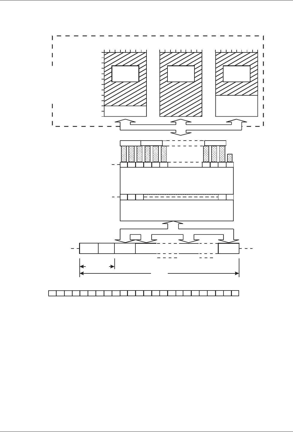
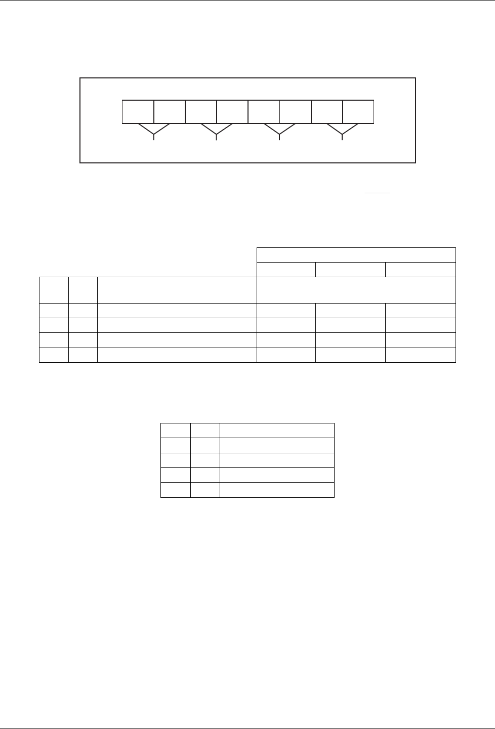
4.4 Frame Structure
Figure 7 shows how an over-air message frame may be constructed from a sequence of: a Symbol Sync
pattern (preamble), a Frame Sync pattern, and one or more 'Header', 'Intermediate' or 'Last' blocks.
Last Block
CRC2
(4 bytes)
µC binary data stored
in MX919B data block
memory configured as
header, intermediate, or
last block by MX919B
task being executed.
Data Bytes
(8)
Data Bytes
(12)
0
1
2
3
4
5
6
7
9
10
11
8
Intermediate BlockHeader Block
CRC 1
(2 bytes)
Byte 7654321076543210 76543210
070
Byte 1
Byte 0Byte 0 Byte 11
0
1
2
345 29303132
0
64 65
4-Level
Symbols
tri-bits
2
1
FEC Trellis Coding / Decoding
(Error Correction)
Interleaving / De-interleaving
7
70
'000'
Symbol
Sync
Frame
Sync
'Header'
Block Intermediate Blocks 'Last'
Block
24 6666 66 66
Frame
Preamble
Frame
-1 +1 +3-3+1 +1 +1-1 -1 -1 -13+3+3 -3-3 +3+3 -3 -3-3 +1+1-1
Frame Sync:
sent first
Over-air
signal
(symbols)
Symbol Sync: at least 24 symbols of '...+3 +3 -3 -3 ...' sequence
last
Data Bytes
(10)
Figure 7: Over-Air Signal Format
The 'Header' block is self-contained and includes its own checksum (CRC1). It would normally carry
information such as the address of the calling and called parties, the number of following blocks in the frame
(if any), and miscellaneous control information. The number of following blocks (if any) is required to allow
the Rx device software to expect the Last Block and interpret it as a Last Block rather than an Intermediate
Block. There is no other indicator to differentiate a Last Block and an Intermediate Block.
The 'Intermediate' block(s) contain only data, the checksum for all of the data in the 'Intermediate' and 'Last'
blocks (CRC2) being contained at the end of the 'Last' block.
This arrangement, while efficient in terms of data capacity, may not be optimum for poor signal-to-noise
conditions, since a reception error in any one of the 'Intermediate' or 'Last' blocks would invalidate the whole
frame. In such conditions, increased throughput may be obtained by using the 'Header' block format for all
blocks of the frame, so blocks that are received correctly can be identified as such, and do not need to be re-
transmitted. These, and some other possible frame structures, are shown in Figure 8.
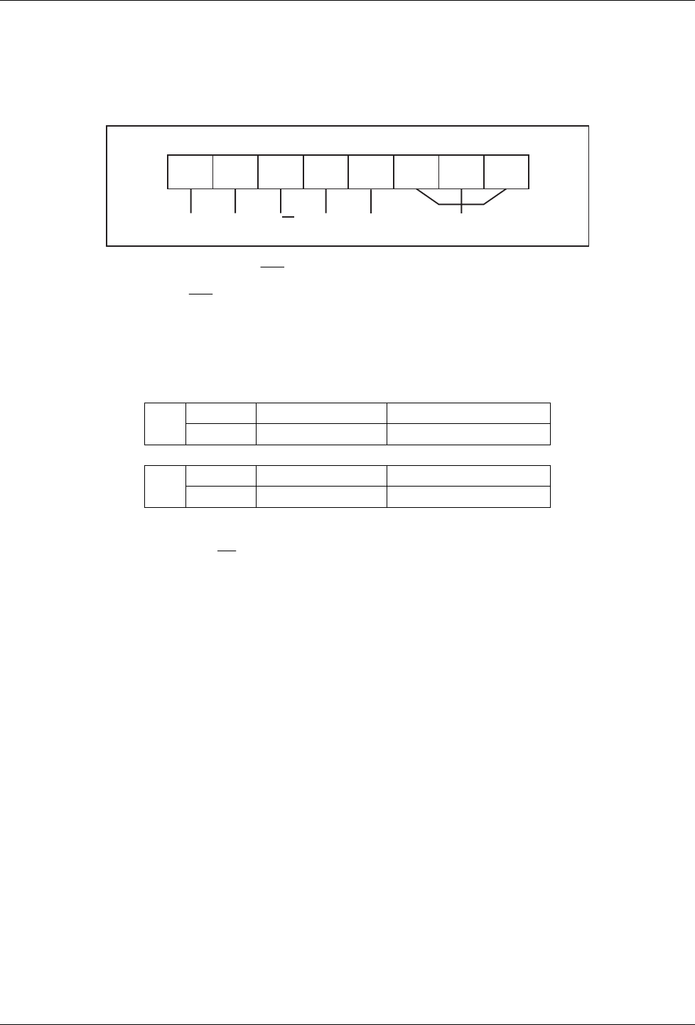
4-Level FSK Modem Data Pump Page 15 of 47 MX919B PRELIMINARY INFORMATION
©2001 MX•COM, INC. www.mxcom.com Tele: 800 638 5577 336 744 5050 Fax: 336 744 5054 Doc. # 20480170.003
4800 Bethania Station Road, Winston-Salem, NC 27105-1201 USA All trademarks and service marks are held by their respective companies.
SYMBOL
SYNC
SYMBOL
SYNC
SYMBOL
SYNC
FRAME
SYNC
FRAME
SYNC
FRAME
SYNC
'LAST'
BLOCK
'HEADER' BLOCKS
'INTERMEDIATE' BLOCKS
'INTERMEDIATE' BLOCKS
A
B
C
Figure 8: Alternative Frame Structures
The MX919B performs the entire block formatting and de-formatting required to convert data between µC
binary form and Over-Air as shown in Figure 7.
4.5 The Programmer’s View
To the programmer, the modem appears as 4 write only 8-bit registers, shadowed by 3 read only registers.
The individual registers are selected by the A0 and A1 chip inputs:
A1 A0 Write to Modem Read from Modem
0 0 Data Buffer Data Buffer
0 1 Command Register Status Register
1 0 Control Register Data Quality Register
1 1 Mode Register Not used
Note: There is a minimum time allowance between accesses of the modem's registers, see Section 6.1.4.
4.5.1 Data Block Buffer
This is a 12-byte read/write buffer used to transfer data (as opposed to command, status, mode, data quality
or control information) between the modem and the host µC.
To the µC, the Data Block Buffer appears as a single 8-bit register. The modem ensures that sequential µC
reads or writes to the buffer are routed to the correct locations within the buffer.
The µC should only access this buffer when the Status Register BFREE (Buffer Free) bit is '1'.
The buffer should only be written to while in Tx mode and read from while in Rx mode. Note that in receive
mode, the modem will function correctly even if the received data is not read from the Data Buffer by the µC.
4.5.2 Command Register
Writing to this register tells the modem to perform a specific task as indicated by the TASK bits and modified
by the AQSC, AQLEV, CRC, and TXIMP bits.
76543210
Command Register
AQSC TXIMP Reserved
Set to '0'
TASK
AQLEV CRC
When there is no action to perform, the modem will be in an 'idle' state. If the modem is in transmit mode, the
input to the Tx RRC filter will be connected to VBIAS. In receive mode, the modem will continue to measure
the received data quality and extract symbols from the received signal, supplying them to the de-interleave
buffer, otherwise these received symbols are ignored.

4-Level FSK Modem Data Pump Page 16 of 47 MX919B PRELIMINARY INFORMATION
©2001 MX•COM, INC. www.mxcom.com Tele: 800 638 5577 336 744 5050 Fax: 336 744 5054 Doc. # 20480170.003
4800 Bethania Station Road, Winston-Salem, NC 27105-1201 USA All trademarks and service marks are held by their respective companies.
4.5.2.1 Command Register B7: AQSC - Acquire Symbol Clock
This bit has no effect in transmit mode.
In receive mode, when a byte with the AQSC bit set to '1' is written to the Command Register, and TASK is
not set to RESET, it initiates an automatic sequence designed to achieve symbol timing synchronization with
the received signal as quickly as possible. This involves setting the Phase Locked Loop of the received bit
timing extraction circuits to its widest bandwidth, then gradually reducing the bandwidth as timing
synchronization is achieved, until it reaches the 'normal' value set by the PLLBW bits of the Control Register.
Setting this bit to '0' (or changing it from '1' to '0') has no effect, however; the acquisition sequence will be re-
started every time a byte written to the Command Register has the AQSC bit set to '1'.
The use of the symbol clock acquisition sequence is described in Section 5.3.
4.5.2.2 Command Register B6: AQLEV - Acquire Receive Signal Levels
This bit has no effect in transmit mode.
In receive mode, when a byte with the AQLEV bit set to '1' is written to the Command Register and TASK is
not set to RESET, it initiates an automatic sequence designed to measure the amplitude and DC offset of the
received signal as rapidly as possible. This sequence involves setting the measurement circuits to respond
quickly at first, then gradually increasing their response time, therefore improving the measurement accuracy,
until the 'normal' value set by the LEVRES bits of the Control Register is reached.
Setting this bit to '0' (or changing it from '1' to '0') has no effect, however; the acquisition sequence will be re-
started every time a byte written to the Command Register has the AQLEV bit set to '1'.
The use of the level measurement acquisition sequence (AQLEV) is described in Section 5.3.
4.5.2.3 Command Register B5: CRC
This bit allows the user to select between two different initial states of the CRC1 and CRC2 checksum
generators. When this bit is set to ‘0’, the CRC generators are initialized to ‘all ones’ as for CCITT X25 CRC
calculations. When this bit is set to ‘1’, the CRC generators are initialized to ‘all zeros’. Setting this bit to ‘0’
provides compatibility with the MX919, a prior member of the MX919 device family. Other systems may set
this bit as required. Note: This bit must be set correctly every time the Command Register is written to.
4.5.2.4 Command Register B4: TXIMP - Tx Level/Impulse Shape
This bit allows the user to choose between two transmit symbol waveform shapes as described in
Section 4.7. Note: This bit must be set correctly every time the Command Register is written to.
4.5.2.5 Command Register B3 - Reserved
This bit should always be set to '0'.
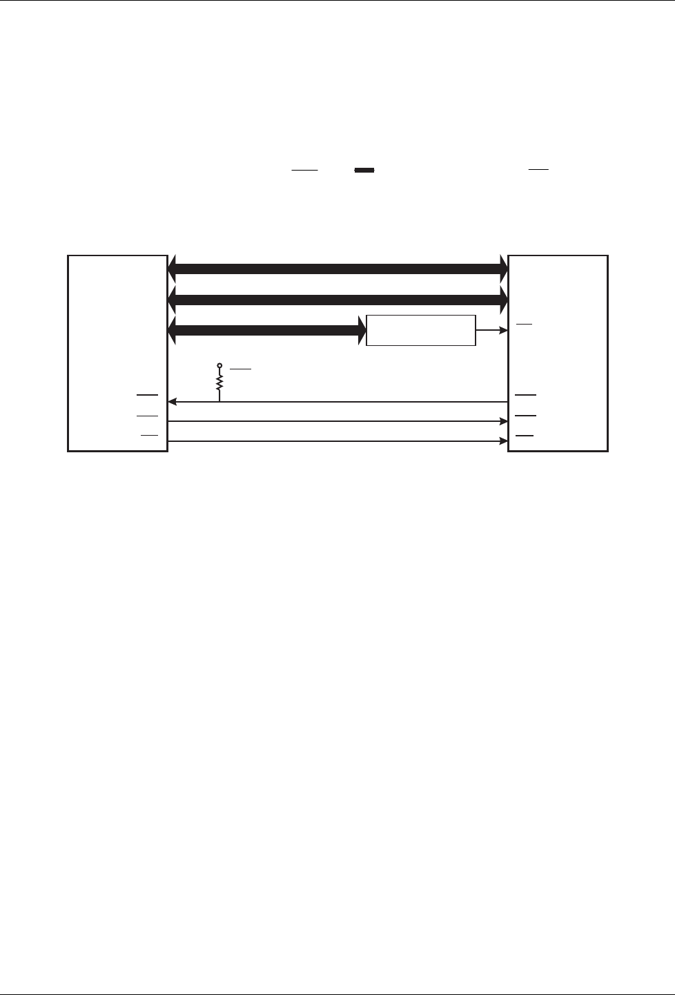
4.5.2.6 Command Register B2, B1, B0: TASK
Operations such as transmitting or receiving a data block are treated by the modem as 'tasks' and are
initiated when the µC writes a byte to the Command Register with the TASK bits set to anything other than
the 'NULL' code.
The µC should not write a task (other than NULL or RESET) to the Command Register or write to or read
from the Data Buffer when the BFREE (Buffer Free) bit of the Status Register is '0'.
Different tasks apply in receive and transmit modes.
When the modem is in transmit mode, all tasks other than NULL or RESET instruct the modem to transmit
data from the Data Buffer, formatting it as required. The µC should therefore wait until the BFREE (Buffer
Free) bit of the Status Register is '1', before writing the data to the Data Block Buffer, then it should write the
desired task to the Command Register. If more than 1 byte needs to be written to the Data Block Buffer, byte
number 0 of the block should be written first.
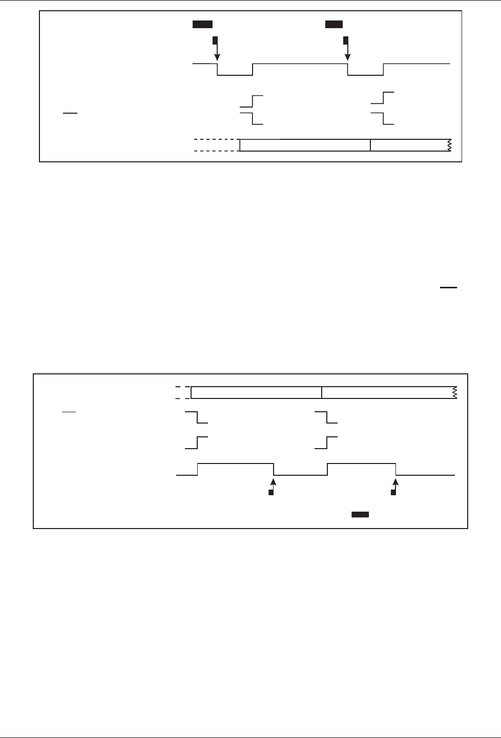
Once the byte containing the desired task has been written to the Command Register, the modem will:
Set the BFREE (Buffer Free) bit of the Status Register to '0'.
Take the data from the Data Block Buffer as quickly as it can - transferring it to the Interleave Buffer for
eventual transmission. This operation will start immediately if the modem is 'idle' (i.e. not transmitting data
from a previous task), otherwise it will be delayed until there is sufficient room in the Interleave Buffer.
Once all of the data has been transferred from the Data Block Buffer, the modem will set the BFREE and IRQ
bits of the Status Register to '1', (causing the chip IRQ output to go low if the IRQEN bit of the Mode Register
has been set to '1') to tell the µC that it may write new data and the next task to the modem.
This lets the µC write the next task and its associated data to the modem while the modem is still transmitting
the data from its previous task.
4-Level FSK Modem Data Pump Page 17 of 47 MX919B PRELIMINARY INFORMATION
©2001 MX•COM, INC. www.mxcom.com Tele: 800 638 5577 336 744 5050 Fax: 336 744 5054 Doc. # 20480170.003
4800 Bethania Station Road, Winston-Salem, NC 27105-1201 USA All trademarks and service marks are held by their respective companies.
TXOUT Signal from Task 1 from Task 2
Task 1 data Task 2 data
Data from C to Block Bufferµ
Task from C to Command
Register
µ
IRQ Bit of Status Register
BFREE Bit of Status Register
IRQ Output (IRQEN = '1')
Figure 9: Transmit Task Overlapping
When the modem is in receive mode, the µC should wait until the BFREE bit of the Status Register is '1', then
write the desired task to the Command Register.
Once the byte containing the desired task has been written to the Command Register, the modem will:
Set the BFREE bit of the Status Register to '0'.
Wait until enough received symbols are in the De-interleave Buffer.
Decode them as needed and transfer the resulting binary data to the Data Block Buffer
Then the modem will set the BFREE and IRQ bits of the Status Register to '1', (causing the IRQ output
to go low if the IRQEN bit of the Mode Register has been set to '1') to tell the µC that it may read from
the Data Block Buffer and write the next task to the modem. If more than 1 byte is contained in the
buffer, byte number 0 of the data will be read out first.
In this way, the µC can read data and write a new task to the modem while the received symbols needed for
this new task are being received and stored in the De-interleave Buffer.
RXIN Signal for Task 1 for Task 2
IRQ Output (IRQEN = '1')
IRQ Bit of Status Register
BFREE Bit of Status Register
Task 1 Task 2
Task 1 data
Data from Block Buffer to Cµ
Task from C
to Command Register
µ
Figure 10: Receive Task Overlapping
Detailed timings for the various tasks are provide in Figure 11 and Figure 12.

4-Level FSK Modem Data Pump Page 18 of 47 MX919B PRELIMINARY INFORMATION
©2001 MX•COM, INC. www.mxcom.com Tele: 800 638 5577 336 744 5050 Fax: 336 744 5054 Doc. # 20480170.003
4800 Bethania Station Road, Winston-Salem, NC 27105-1201 USA All trademarks and service marks are held by their respective companies.
MX919B Modem Tasks:
B2 B1 B0 Receive Mode Transmit Mode
0 0 0 NULL NULL
0 0 1 SFSH Search for FS + Header T24S Transmit 24 symbols
0 1 0 RHB Read Header Block THB Transmit Header Block
0 1 1 RILB Read Intermediate or Last Block TIB Transmit Intermediate Block
1 0 0 SFS Search for Frame sync TLB Transmit Last Block
1 0 1 R4S Read 4 symbols T4S Transmit 4 symbols
1 1 0 NULL NULL
1 1 1 RESET Cancel any current action RESET Cancel any current action
4.5.2.7 NULL: No effect
This 'task' is provided so an AQSC or AQLEV command can be initiated without loading a new task.
4.5.2.8 SFSH: Search for Frame Sync plus Header Block
This task causes the modem to search the received signal for a valid 24-symbol Frame Sync sequence
followed by Header Block which has a correct CRC1 checksum.
The task continues until a valid Frame Sync plus Header Block has been found.
The search consists of two stages:
First the modem will attempt to match the incoming symbols against the 24-symbol Frame
Synchronization pattern to within the tolerance defined by the FSTOL bits of the Control Register.
Once a match has been found, the modem will read in the next 66 symbols as if they were a 'Header'
block, decoding the symbols and checking the CRC1 checksum. If this is incorrect, the modem will
resume the search, looking for a fresh Frame Sync pattern.
If the received CRC1 is correct, the 10 decoded data bytes will be placed into the Data Block Buffer, the
BFREE and IRQ bits of the Status Register will be set to '1' and the CRCERR bit cleared to '0'.
Once detecting that the BFREE bit of the Status Register has gone to '1', the µC should read the 10 bytes
from the Data Block Buffer and then write the next task to the modem's Command Register.
4.5.2.9 RHB: Read Header Block
This task causes the modem to read the next 66 symbols as a 'Header' Block, decoding them, placing the
resulting 10 data bytes and the 2 received CRC1 bytes into the Data Block Buffer, and setting the BFREE and
IRQ bits of the Status Register to '1'. When the task is complete, it indicates that the µC may read the data
from the Data Block Buffer and write the next task to the modem's Command Register.
The CRCERR bit of the Status Register will be set to '1' or '0' depending on the validity of the received CRC1
checksum bytes.
4.5.2.10 RILB: Read 'Intermediate' or 'Last' Block
This task causes the modem to read the next 66 symbols as an 'Intermediate' or 'Last' block (the µC should
be able to tell from the 'Header' block how many blocks are in the frame and when to expect the 'Last' block).
In each case, it will decode the 66 symbols and place the resulting 12 bytes into the Data Block Buffer, setting
the BFREE and IRQ bits of the Status Register to '1' when the task is complete.
If an 'Intermediate' block is received, then the µC should read out all 12 bytes from the Data Block Buffer and
ignore the CRCERR bit of the Status Register, for a 'Last' block the µC need only read the first 8 bytes from
the Data Block Buffer, and the CRCERR bit in the Status Register will reflect the validity of the received CRC2
checksum.
4.5.2.11 SFS: Search for Frame Sync
This task causes the modem to search the received signal for a 24-symbol sequence which matches the
Frame Synchronization pattern to within the tolerance defined by the FSTOL bits of the Mode Register.
When a match is found the modem will set the BFREE and IRQ bits of the Status Register to '1' to indicate to
the µC that it should write the next task to the Command Register.

4-Level FSK Modem Data Pump Page 19 of 47 MX919B PRELIMINARY INFORMATION
©2001 MX•COM, INC. www.mxcom.com Tele: 800 638 5577 336 744 5050 Fax: 336 744 5054 Doc. # 20480170.003
4800 Bethania Station Road, Winston-Salem, NC 27105-1201 USA All trademarks and service marks are held by their respective companies.
4.5.2.12 R4S: Read 4 Symbols
This task causes the modem to read the next 4 symbols and translate them directly (without de-interleaving or
FEC) to an 8-bit byte which is placed into the Data Block Buffer. The BFREE and IRQ bits of the Status
Register are then set to '1' to indicate that the µC may read the data byte from the Data Block Buffer and write
the next task to the Command Register.
This task is intended for special tests and channel monitoring - perhaps preceded by a SFS task.
Note: It is possible to construct message formats, which do not rely on the block formatting of the THB, TIB,
and TLB tasks. This can be accomplished by using T4S or T24S tasks to transmit and R4S to receive the
user's data. One should be aware, that the receive level and timing measurement circuits need to see a
reasonably 'random' distribution of all four possible symbols in the received signal to operate correctly.
Accordingly, binary data may benefit from scrambling before transmission if it is not reasonably 'random' to
start with.
4.5.2.13 T24S: Transmit 24 Symbols
This task, which is intended to facilitate the transmission of Symbol and Frame Sync patterns as well as
special test sequences, takes 6 bytes of data from the Data Block Buffer and transmits them as 24 4-level
symbols without any CRC or FEC.
Byte 0 of the Data Block Buffer is sent first, byte 5 last.
Once the modem has read the data bytes from the Data Block Buffer, the BFREE and IRQ bits of the Status
Register will be set to '1', indicating to the µC that it may write the data and command byte for the next task to
the modem.
The tables below show what data needs to be written to the Data Block Buffer to transmit the MX919B
Symbol and Frame Sync sequences:
Values written to Data Block Buffer
‘Symbol Sync’
Symbols Binary Hex
+3 +3 -3 -3 Byte 0: 11110101 F5
+3 +3 -3 -3 Byte 1: 11110101 F5
+3 +3 -3 -3 Byte 2: 11110101 F5
+3 +3 -3 -3 Byte 3: 11110101 F5
+3 +3 -3 -3 Byte 4: 11110101 F5
+3 +3 -3 -3 Byte 5: 11110101 F5
Values written to Data Block Buffer
‘Frame Sync’
Symbols Binary Hex
-1 +1 -1 +1 Byte 0: 00100010 22
-1 +3 -3 +3 Byte 1: 00110111 37
-3 -1 +1 -3 Byte 2: 01001001 49
+3 +3 -1 +1 Byte 3: 11110010 F2
-3 -3 +1 +3 Byte 4: 01011011 5B
-1 -3 +1 +3 Byte 5: 00011011 1B
4.5.2.14 THB: Transmit Header Block
This task takes 10 bytes of data (Address and Control) from the Data Block Buffer, calculates and appends
the 2-byte CRC1 checksum, translates the result to 4-level symbols (with FEC), interleaves the symbols, and
transmits the result as a formatted 'Header' Block.
Once the modem has read the data bytes from the Data Block Buffer, the BFREE and IRQ bits of the Status
Register will be set to '1'.

4-Level FSK Modem Data Pump Page 20 of 47 MX919B PRELIMINARY INFORMATION
©2001 MX•COM, INC. www.mxcom.com Tele: 800 638 5577 336 744 5050 Fax: 336 744 5054 Doc. # 20480170.003
4800 Bethania Station Road, Winston-Salem, NC 27105-1201 USA All trademarks and service marks are held by their respective companies.
4.5.2.15 TIB: Transmit Intermediate Block
This task takes 12 bytes of data from the Data Block Buffer, updates the 4-byte CRC2 checksum for inclusion
in the 'Last' block, translates the 12 data bytes to 4-level symbols (with FEC), interleaves the symbols, and
transmits the result as a formatted 'Intermediate' Block.
Once the modem has read the data bytes from the Data Block Buffer, the BFREE and IRQ bits of the Status
Register will be set to '1'.
4.5.2.16 TLB: Transmit Last Block
This task takes 8 bytes of data from the Data Block Buffer, updates and appends the 4-byte CRC2 checksum,
translates the resulting 12 bytes to 4-level symbols (with FEC), interleaves the symbols, and transmits the
result as a formatted 'Last' Block.
Once the modem has read the data bytes from the Data Block Buffer, the BFREE and IRQ bits of the Status
Register will be set to '1'.
4.5.2.17 T4S: Transmit 4 Symbols
This command is similar to T24S but takes only one byte from the Data Block Buffer, transmitting it as four 4-
level symbols.
4.5.2.18 RESET: Stop any current action
This 'task' takes effect immediately, and terminates any current action (task, AQSC or AQLEV) the modem
may be performing and sets the BFREE bit of the Status Register to '1', without setting the IRQ bit. It should
be used when VDD is applied, to set the modem into a known state.
Note: Due to delays in the transmit filter, it will take several symbol times for any change to appear at the
TXOUT pin.
4.5.2.19 Task Timing
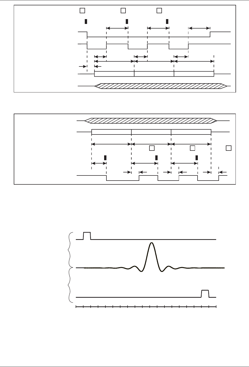
The following table and figures describe the duration of tasks and timing sequences for Tx and Rx operation.
Task Time
(symbol times)
t1 Modem Idle state. Time from writing first task to application of first
transmit bit to Tx RRC filter.
Any 1 to 2
t2 Time from application of first symbol of the task to the Tx RRC filter
until BFREE goes to a logic ‘1’.
T24S
THB/TIB/TLB
T4S
5
16
0
t3 Time to transmit all symbols of the task.
T24S
THB/TIB/TLB
T4S
24
66
4
t4 Max time allowed from BFREE going to a logic ‘1’ (high) for next task
(and data) to be written to modem.
T24S
THB/TIB/TLB
T4S
18
49
3
t5 Time to receive all symbols of task.
SFS
SFSH
RHB/RILB
R4S
24 (minimum)
90 (minimum)
66
4
t6 Maximum time between first symbol of task entering the de-interleave
circuit and the task being written to modem.
SFS
SFSH
RHB/RILB
R4S
21
21
49
3
t7 Maximum time from the last bit of the task entering the de-interleave
circuit to BFREE going to a logic ‘1’ (high).
Any 1
4-Level FSK Modem Data Pump Page 21 of 47 MX919B PRELIMINARY INFORMATION
©2001 MX•COM, INC. www.mxcom.com Tele: 800 638 5577 336 744 5050 Fax: 336 744 5054 Doc. # 20480170.003
4800 Bethania Station Road, Winston-Salem, NC 27105-1201 USA All trademarks and service marks are held by their respective companies.
from Task 2 from Task 3
from Task 1
t1
t2
Task to Command Register
Data to Data Block Buffer
t3
t4
Modem Tx Output
12
1 2
Symbols to RRC Filter
3
IBEMPTY Bit
BFREE Bit
3
t2t2t3
t3
t4
t4
Figure 11: Transmit Task Timing Diagram
for Task 2 for Task 3for Task 1
Task to Command Register
Data from Data Block Buffer
Modem Rx Input
12
12
Symbols to De-Interleave
Circuit
3
BFREE Bit
3
t5
t6
t7
t5
t5
t5
t6t6
t7
t7
Figure 12: Receive Task Timing Diagram
4.5.2.20 RRC Filter Delay
The previous task timing figures are based on the signal at the input to the RRC filter (in transmit mode) or the
input to the de-interleave buffer (in receive mode). There is an additional delay of about 8 symbol times
through to the RRC filter in both transmit and receive modes, as illustrated below:
Delay from Rx Input
(from FM discriminator)
to interpreted data in
internal buffer. RX Symbol to De-Interleave Buffer
Tx Symbol at TXOUT pin / Rx Symbol from FM discriminator
Symbol-times
Tx Symbol to RRC Filter
Delay from Tx Input
symbol to TXOUT
response.
Figure 13: RRC Low Pass Filter Delay
4-Level FSK Modem Data Pump Page 22 of 47 MX919B PRELIMINARY INFORMATION
©2001 MX•COM, INC. www.mxcom.com Tele: 800 638 5577 336 744 5050 Fax: 336 744 5054 Doc. # 20480170.003
4800 Bethania Station Road, Winston-Salem, NC 27105-1201 USA All trademarks and service marks are held by their respective companies.
4.5.3 Control Register
This 8-bit write-only register controls the modem's symbol rate, the response times of the receive clock
extraction, signal level measurement circuits, and the Frame Sync pattern recognition tolerance to inexact
matches.
76543210
Control Register
FSTOL LEVRES PLLBW
CKDIV
4.5.3.1 Control Register B7, B6: CKDIV - Clock Division Ratio
These bits control a frequency divider driven from the clock signal present at the XTAL pin, therefore
determining the nominal symbol rate. Because each symbol represents two bits, bit rates are 2x the symbol
rates. The table below shows how symbol rates of 2400/4800/9600 symbols/sec (4800/9600/19200bps) may
be obtained from common Xtal frequencies:
Xtal Frequency (MHz)
2.4576 4.9152 9.8304
B7 B6 Division Ratio:
Xtal Frequency/Symbol Rate
Symbol Rate (symbols/sec) / Bit Rate
(bps)
0 0 512 4800/9600 9600/19200
0 1 1024 2400/4800 4800/9600 9600/19200
1 0 2048 2400/4800 4800/9600
1 1 4096 2400/4800
4.5.3.2 Control Register B5, B4: FSTOL - Frame Sync Tolerance to Inexact Matches
These two bits have no effect in transmit mode. In receive mode, they define the maximum number of
mismatches allowed during a search for the Frame Sync pattern:
B5 B4 Mismatches allowed
0 0 0
0 1 2
1 0 4
1 1 6
Note: A single 'mismatch' is defined as the difference between two adjacent symbol levels, thus if the symbol
'+1' were expected, then received symbol values of '+3' and '-1' would count as 1 mismatch, a received
symbol value of '-3' would count as 2 mismatches. A setting of '4 mismatches' is recommended for
normal use.

4-Level FSK Modem Data Pump Page 23 of 47 MX919B PRELIMINARY INFORMATION
©2001 MX•COM, INC. www.mxcom.com Tele: 800 638 5577 336 744 5050 Fax: 336 744 5054 Doc. # 20480170.003
4800 Bethania Station Road, Winston-Salem, NC 27105-1201 USA All trademarks and service marks are held by their respective companies.
4.5.3.3 Control Register B3, B2: LEVRES - Level Measurement Modes
These two bits have no effect in transmit mode. In receive mode they set the 'normal' or 'steady state'
operating mode of the Rx signal amplitude and DC offset measuring and tracking circuits. These circuits
analyze the Rx signal envelope and charge the DOC1 and DOC2 capacitors to 'store' signal maximum and
minimum references that are used in the data reception process. This setting is temporarily overridden during
the automatic sequencing triggered by an AQLEV command when level is initially being acquired as
described in Section 5.3.
B3 B2 Mode
0 0 Hold
0 1 Level Track
1 0 Lossy Peak Detect
1 1 Slow Peak Detect
In normal use the LEVRES bits should be set to '0 1' (Level Track). The other modes are intended for special
purposes, for device testing, or are invoked automatically during an AQLEV sequence.
In 'Slow Peak Detect' modes, the positive and negative excursions of the received signal (after filtering) are
measured by peak rectifiers driving the DOC1 and DOC2 capacitors to establish the amplitude of the signal
and any DC offset with regards to VBIAS. This mode provides good overall performance, particularly when
acquiring level information at the start of a received message, but does not work as well with certain long
sequences of repeated data byte values. It is also susceptible to large amplitude noise spikes, which can be
caused by deep fades.
The 'Lossy Peak Detect' mode is similar to 'Slow Peak Detect' but the capacitor discharge time constant is
much shorter so this mode is not suitable for normal data reception and is only used within part of the
automatic AQLEV acquisition sequence.
In 'Level Track' mode the DOC capacitor voltages are slowly adjusted by the MX919B in such a way as to
minimize the average errors seen in the received signal. This mode provides the best overall performance,
being much more accurate than 'Slow Peak Detect' when receiving large amplitude noise spikes on long
sequences of repeated data byte values. It does, however, depend on the measured levels and timing being
approximately correct. If either of these is significantly wrong then the correction algorithm used by the 'Level
Track' mode can actually drive the voltages on the DOC capacitors away from their optimum levels. For this
reason, the automatic AQLEV acquisition sequence (see Section 5.3) forces the level measuring circuits into
'Slow Peak Detect' mode until a Frame Sync pattern has been found.
4.5.3.4 Control Register B1, B0: PLLBW - Phase-Locked Loop Bandwidth Modes
These two bits have no effect in transmit mode. In receive mode, they set the 'normal' or 'steady state'
bandwidth of the Rx clock extraction Phase Locked Loop circuit. The PLL circuit synchronizes itself with the
Rx Signal to develop a local clock signal used in the data clock recovery process. This setting will be
temporarily overridden during the automatic sequencing of an AQSC command when Rx clock extraction
circuits are initially being trained as described in Section 5.3.
B1 B0 PLL Mode
0 0 Hold
0 1 Level Track
1 0 Lossy Peak Detect
1 1 Slow Peak Detect
The normal setting for the PLLBW bits should be 'Medium Bandwidth' when the received symbol rate and the
frequency of the receiving modem's crystal are both within ±100ppm of nominal, except at the start of a
symbol clock acquisition sequence (AQSC) when 'Wide Bandwidth' should be selected as described in
Section 5.3
If the received symbol rate and the crystal frequency are both within ±20ppm of nominal then selection of the
'Narrow Bandwidth' setting will provide better performance especially through fades or noise bursts which
may otherwise pull the PLL away from its optimum timing. In this case however; it is recommended that the
PLLBW bits only be set to 'Narrow Bandwidth' after the modem has been running in 'Medium Bandwidth'
mode for about 200 symbol times to ensure accurate lock has first been achieved.
4-Level FSK Modem Data Pump Page 24 of 47 MX919B PRELIMINARY INFORMATION
©2001 MX•COM, INC. www.mxcom.com Tele: 800 638 5577 336 744 5050 Fax: 336 744 5054 Doc. # 20480170.003
4800 Bethania Station Road, Winston-Salem, NC 27105-1201 USA All trademarks and service marks are held by their respective companies.
The 'Hold' setting disables the feedback loop of the PLL which continues to run at a rate determined only by
the actual crystal frequency and the setting of the Control Register CKDIV bits, not the PLL's operating
frequency immediately prior to the 'Hold' setting.
4.5.4 Mode Register
The contents of this 8-bit write only register control the basic operating modes of the modem:
76543210
Mode Register
IRQEN RXEYE
INVSYM Set to '000'
Tx/Rx PSAVE
4.5.4.1 Mode Register B7: IRQEN - IRQ Output Enable
When this bit is set to '1', the IRQ chip output pin is pulled low (VSS) given the IRQ bit of the Status Register
is a '1'.
4.5.4.2 Mode Register B6: INVSYM - Invert Symbols
This bit controls the polarity of the transmitted and received symbol voltages.
B6 Symbol Signal at TXOUT Signal at RXAMPOUT
+3 Above VBIAS Below VBIAS
0 -3 Below VBIAS Above VBIAS
+3 Below VBIAS Above VBIAS
1 -3 Above VBIAS Below VBIAS
Note: B6 must be normally set to the same value in Tx and Rx devices for successful operation.
4.5.4.3 Mode Register B5: RXTX/ - Tx/Rx Mode
Setting this bit to '1' places the modem into the Transmit mode, clearing it to '0' puts the modem into the
Receive mode.
Note: Changing between receive and transmit modes will cancel any current task.

4-Level FSK Modem Data Pump Page 25 of 47 MX919B PRELIMINARY INFORMATION
©2001 MX•COM, INC. www.mxcom.com Tele: 800 638 5577 336 744 5050 Fax: 336 744 5054 Doc. # 20480170.003
4800 Bethania Station Road, Winston-Salem, NC 27105-1201 USA All trademarks and service marks are held by their respective companies.
4.5.4.4 Mode Register B4: RXEYE - Show Rx Eye
This bit should normally be set to '0'. Setting it to '1' when the modem is in receive mode configures the
modem for a special test mode, in which the input of the Tx output buffer is connected to the Rx Symbol/Clock
extraction circuit at a point which carries the equalized receive signal. This may be monitored with an
oscilloscope (at the TXOUT pin itself), to assess the quality of the complete radio channel including the Tx
and Rx modem filters, the Tx modulator and the Rx IF filters, and FM demodulator.
This mode is provided because observation of the direct discriminator output of a root raised cosine Tx filtered
signal (before Rx equalization) is not very recognizable so it is generally not useful.
The resulting eye diagram (for reasonably random data) should ideally be as shown in the following Figure
14, with 4 distinct and equally spaced level crossing points.
Figure 14: Ideal 'RXEYE' Signal
Note: A two-channel oscilloscope is needed for this testing. One channel of the oscilloscope should be
placed on the signal path of interest, such as the Tx output. If the Rx eye diagram is to be viewed, set
the “RXEYE” bit in the Mode Register to “1” and connect the oscilloscope probe downstream of the
external RC filter on the TXOUT pin. (This Mode Register bit causes the MX919B to enter a special
test mode whereby the Rx output is placed on the TXOUT pin. This mode is provided because
observation of the direct discriminator output of a root raised cosine Tx filtered signal is not very
recognizable and is generally not useful.)
The other oscilloscope channel should be used for triggering and should ideally be placed on the
transmitting MX919B IRQ pin. This will allow the triggering to be synchronized with the completion of
each transmitted data word. If this triggering location is not practical, use the receiving MX919B
IRQ signal for triggering. The falling edge of the IRQ line should be used for triggering. The data
stream used for this testing should have a reasonably random structure.
4.5.4.5 Mode Register B3: PSAVE - Powersave
When this bit is a ‘1’, the modem will be in a ‘powersave’ mode in which the internal filters, the Rx Symbol and
Clock extraction circuits, and the Tx output buffer will be disabled. The TXOUT pin will be connected to VBIAS
through a high value internal resistance. The Xtal clock oscillator, Rx input amplifier and the µC interface
logic will continue to operate.
Setting the PSAVE bit to ‘0’ restores power to all of the chip circuitry.
Note: The internal filters, and therefore the TXOUT pin in transmit mode, will take approximately 20 symbol-
times to settle after the PSAVE bit has gone from ‘1’ to ‘0’.
4.5.4.6 Mode Register B2, B1, B0
These bits should be set to '000'.

4-Level FSK Modem Data Pump Page 26 of 47 MX919B PRELIMINARY INFORMATION
©2001 MX•COM, INC. www.mxcom.com Tele: 800 638 5577 336 744 5050 Fax: 336 744 5054 Doc. # 20480170.003
4800 Bethania Station Road, Winston-Salem, NC 27105-1201 USA All trademarks and service marks are held by their respective companies.
4.5.5 Status Register
This register may be read by the µC to determine the current state of the modem.
76543210
Status Register
IRQ DIBOVFBFREE Reserved
IBEMPTY CRCERR
4.5.5.1 Status Register B7: IRQ - Interrupt Request
This bit is set to '1' by:
The Status Register BFREE bit going from '0' to '1', unless this is caused by a RESET task or by a
change to the Mode Register TX RX/ or PSAVE bits
or The Status Register IBEMPTY bit going from '0' to '1', unless this is caused by a RESET task or by
changing the Mode Register TX RX/ or PSAVE bits.
or The Status Register DIBOVF bit going from '0' to '1'.
The IRQ bit is cleared to '0' immediately after a read of the Status Register.
If the IRQEN bit of the Mode Register is '1', then the chip IRQ output will be pulled low (VSS) when the IRQ
bit is set to '1', and will go high impedance when the Status Register is read.
4.5.5.2 Status Register B6: BFREE - Data Block Buffer Free
This bit reflects the availability of the Data Block Buffer and is cleared to '0' when a task other than NULL or
RESET is written to the Command Register.
In transmit mode, the BFREE bit will be set to '1' (also setting the Status Register IRQ bit to '1') by the modem
when the modem is ready for the µC to write new data to the Data Block Buffer and the next task to the
Command Register.
In receive mode, the BFREE bit is set to '1' (also setting the Status Register IRQ bit to '1') by the modem
when it has completed a task and any data associated with that task has been placed into the Data Block
Buffer. The µC may then read that data and write the next task to the Command Register.
The BFREE bit is also set to '1' - but without setting the IRQ bit - by a RESET task or when the Mode Register
TX RX/ or PSAVE bits are changed.
4.5.5.3 Status Register B5: IBEMPTY - Interleave Buffer Empty
In transmit mode, this bit will be set to '1' - also setting the IRQ bit - when less than two symbols remain in the
Interleave Buffer. Any transmit task written to the modem after this bit goes to '1' will be too late to avoid a
gap in the transmit output signal.
The bit is also set to '1' by a RESET task or by a change of the Mode Register TX RX/ or PSAVE bits, but in
these cases the IRQ bit will not be set.
The bit is cleared to '0' within one symbol time after a task other than NULL or RESET is written to the
Command Register.
Note: When the modem is in transmit mode and the Interleave Buffer is empty, a mid-level (halfway between
'+1' and '-1') signal will be sent to the RRC filter.
In receive mode this bit will be '0'.
4.5.5.4 Status Register B4: DIBOVF - De-Interleave Buffer Overflow
In receive mode this bit will be set to '1' - also setting the IRQ bit - when a RHB, RILB or R4S task is written to
the Command Register too late to allow continuous reception.
The bit is cleared to '0' immediately after reading the Status Register, by writing a RESET task to the
Command Register or by changing the TX RX/or PSAVE bits of the Mode Register.
In transmit mode this bit will be '0'.

4-Level FSK Modem Data Pump Page 27 of 47 MX919B PRELIMINARY INFORMATION
©2001 MX•COM, INC. www.mxcom.com Tele: 800 638 5577 336 744 5050 Fax: 336 744 5054 Doc. # 20480170.003
4800 Bethania Station Road, Winston-Salem, NC 27105-1201 USA All trademarks and service marks are held by their respective companies.
4.5.5.5 Status Register B3: CRCERR - CRC Checksum Error
In receive mode, this bit will be updated at the end of a SFSH, RHB or RILB task to reflect the result of the
receive CRC check. '0' indicates that the CRC was received correctly, '1' indicates an error.
Note: This bit should be ignored when an 'Intermediate' block (which does not have an integral CRC) is
received.
The bit is cleared to '0' by a RESET task or by changing the TX RX/, or PSAVE bits of the Mode Register. In
transmit mode this bit is '0'.
4.5.5.6 Status Register B2, B1, B0
These bits are reserved for future use.
4.5.6 Data Quality Register
In receive mode, the MX919B continually measures the 'quality' of the received signal, by comparing the
actual received waveform over the previous 64 symbol times against an internally generated 'ideal' 4-level
FSK baseband signal.
The result is placed into bits 3-7 of the Data Quality Register for the µC to read at any time, bits 0-2 being
always set to '0'. Figure 15 shows how the value (0-255) read from the Data Quality Register varies with
received signal-to-noise ratio:
7
59111315
0
50
100
150
200
250
DQ
S/N dB (noise in 2 x symbol-rate bandwidth)
Figure 15: Typical Data Quality Reading vs S/N
The Data Quality readings are only valid when the modem has successfully acquired signal level and timing
lock for at least 64 symbol times. It is invalid when an AQSC or AQLEV sequence is being performed or
when the LEVRES setting is 'Lossy Peak Detect'. A low reading will be obtained if the PLLBW bits are set to
'Wide' or if the received signal waveform is distorted in any significant way.
Section 5.6 describes how monitoring the Data Quality reading can help improve the overall system
performance in some applications.
4.6 CRC, FEC, and Interleaving
4.6.1 Cyclic Redundancy Codes
4.6.1.1 CRC1
This is a sixteen-bit CRC check code contained in bytes 10 and 11 of the Header Block, which provides error
detection coverage for the Header Block of a message. It is calculated by the modem from the first 80 bits of
the Header Block (Bytes 0 to 9 inclusive) using the generator polynomial:
x16 + x12 + x5 + 1
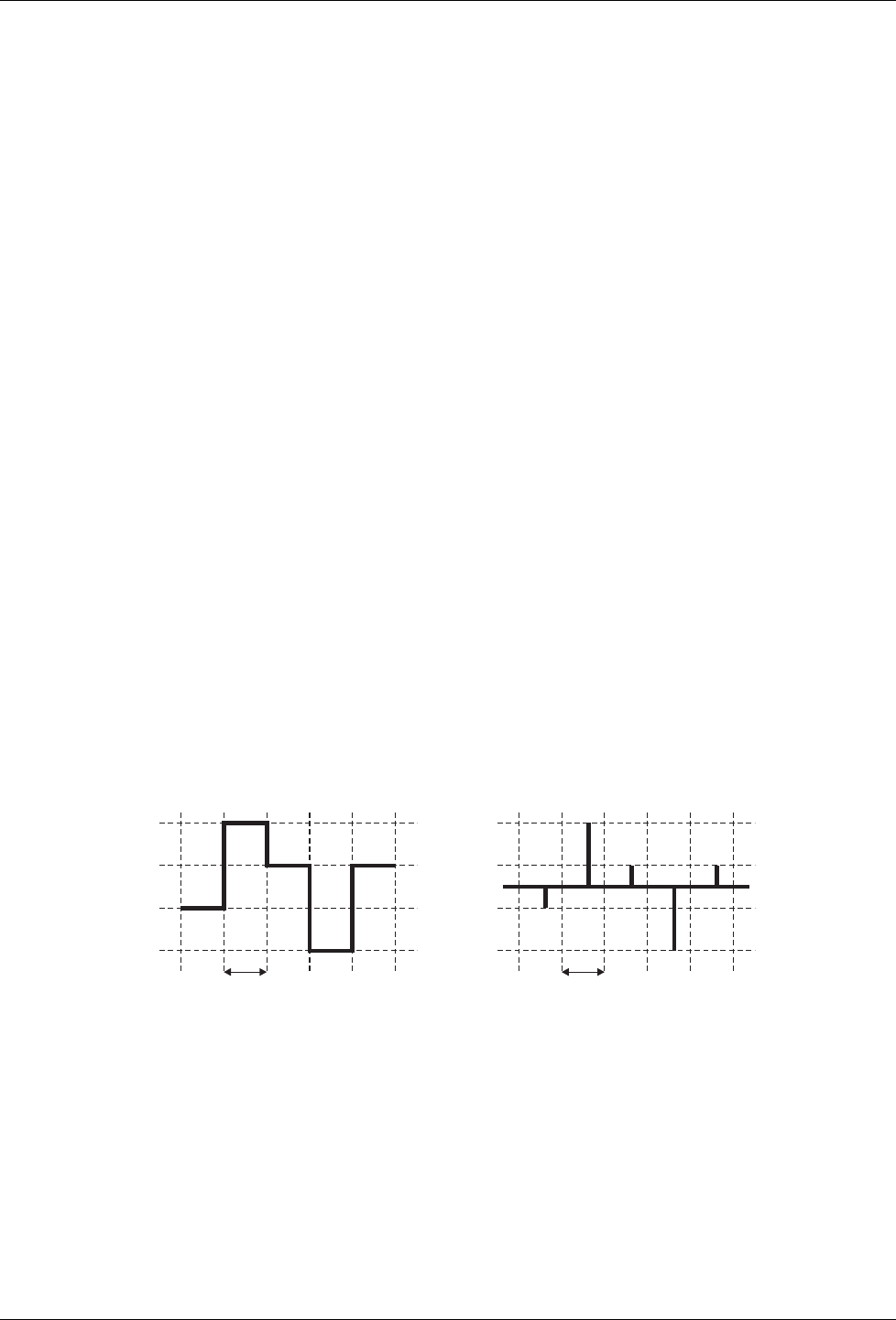
4-Level FSK Modem Data Pump Page 28 of 47 MX919B PRELIMINARY INFORMATION
©2001 MX•COM, INC. www.mxcom.com Tele: 800 638 5577 336 744 5050 Fax: 336 744 5054 Doc. # 20480170.003
4800 Bethania Station Road, Winston-Salem, NC 27105-1201 USA All trademarks and service marks are held by their respective companies.
4.6.1.2 CRC2
This is a thirty-two-bit CRC check code contained in bytes 8 to 11 of the 'Last' Block, which provides error
detection coverage for the combined Intermediate Blocks and Last Block of a message. It is calculated by the
modem from all of the data and pad bytes in the Intermediate Blocks and in the first 8 bytes of the Last Block
using the generator polynomial:
x32 + x26 + x23 + x22 + x16 + x12 + x11 + x10 + x8 + x7 + x5 + x4 + x2 + x1 + 1
Note: In receive mode the CRC2 checksum circuits are initialized on completion of any task other than NULL
or RILB. In transmit mode the CRC2 checksum circuits are initialized on completion of any task other
than NULL, TIB, or TLB.
Command Register bit B5 (CRC) allows the user to select between two different forms of the CRC1
and CRC2 checksums. When this bit is set to '0', the CRC generators are initialized to 'all ones' for
calculations such as CCITT X25 CRC. When this bit is set to '1', the CRC generators are initialized to
'all zeros'.
4.6.1.3 Forward Error Correction
In transmit mode, the MX919B uses a Trellis Encoder to translate the 96 bits (12 bytes) of a 'Header',
'Intermediate' or 'Last' Block into a 66-symbol (132 bits) sequence which includes FEC information.
In receive mode, the MX919B decodes the received 66 symbols of a block into 96 bits of binary data using a
'Soft Decision' Viterbi algorithm to perform decoding and error correction.
4.6.1.4 Interleaving
The 66 symbols of a 'Header', 'Intermediate' or 'Last' block are interleaved by the modem before transmission
to provide protection against the effects of noise bursts and short fades.
In receive mode, the MX919B de-interleaves the received symbols prior to decoding.
4.7 Transmitted Symbol Shape
Bit 4 of the Command Register (TXIMP) selects the transmit baseband signal and the receive signal
equalization as follows:
If the TXIMP bit is '0', then the transmit baseband signal is generated by feeding full-symbol-time-width 4-level
symbols into the RRC lowpass filter. The receive signal equalization is optimized for this type of signal. With
this setting, the MX919B is compatible with the MX919A devices, another member of the MX919 device
family.
If the TXIMP bit is set to '1,' impulses, rather than full-symbol-time-width symbols are fed into the RRC filter
when in TX mode, and the receive signal equalization is suitably adjusted in RX mode.
1 symbol
time
+3
TXIMP = 0 TXIMP = 1
-1
+1
-3
1 symbol
time
+3
-1
+1
-3
Figure 16: Input Signal to RRC Filter in Tx Mode for TXIMP = 0 and 1
4-Level FSK Modem Data Pump Page 29 of 47 MX919B PRELIMINARY INFORMATION
©2001 MX•COM, INC. www.mxcom.com Tele: 800 638 5577 336 744 5050 Fax: 336 744 5054 Doc. # 20480170.003
4800 Bethania Station Road, Winston-Salem, NC 27105-1201 USA All trademarks and service marks are held by their respective companies.
Figure 17: Tx Signal Eye TXIMP = 0
Figure 18: Tx Signal Eye TXIMP = 1
Note: Setting TXIMP to '1' affects the Tx output signal level as shown in Section 6.1.3 and the table below.
TXIMP = 0 TXIMP = 1
Nominal Voltage difference between continuous ‘+3’ and
continuous ‘-3’ symbol outputs
0.157VDD 0.157VDD
Nominal VP-P for continuous ‘+3+3-3-3…’ symbol pattern. 0.20VDD 0.22VDD

4-Level FSK Modem Data Pump Page 30 of 47 MX919B PRELIMINARY INFORMATION
©2001 MX•COM, INC. www.mxcom.com Tele: 800 638 5577 336 744 5050 Fax: 336 744 5054 Doc. # 20480170.003
4800 Bethania Station Road, Winston-Salem, NC 27105-1201 USA All trademarks and service marks are held by their respective companies.
5. Application
5.1 Transmit Frame Example
The operations needed to transmit a single Frame consisting of Symbol and Frame Sync sequences, and one
each Header, Intermediate and Last blocks are provided below:
1. Ensure that the Control Register has been loaded with a suitable CKDIV value, that the IRQEN and
T
XRX/ bits of the Mode Register are '1', the RXEYE and PSAVE bits are '0', and the INVSYM bit is set
appropriately.
2. Read the Status Register to ensure that the BFREE bit is '1', then write 6 Symbol Sync bytes (a
preamble) to the Data Block Buffer and a T24S task to the Command Register.
3. Wait for an interrupt from the modem, read the Status Register; the IRQ and BFREE bits should be '1'
and the IBEMPTY bit should be '0'.
4. Write 6 byte Frame Sync to the Data Block Buffer and a T24S task to the Command Register.
5. Wait for an interrupt from the modem, read the Status Register; the IRQ and BFREE bits should be '1'
and the IBEMPTY bit should be '0'.
6. Write 10 Header Block bytes to the Data Block Buffer and a THB task to the Command Register.
7. Wait for an interrupt from the modem, read the Status Register; the IRQ and BFREE bits should be '1'
and the IBEMPTY bit should be '0'.
8. Write 12 Intermediate Block bytes to the Data Block Buffer and a TIB task to the Command Register.
9. Wait for an interrupt from the modem, read the Status Register; the IRQ and BFREE bits should be '1'
and the IBEMPTY bit should be '0'.
10. Write 8 Last Block bytes to the Data Block Buffer and a TLB task to the Command Register.
11. Wait for an interrupt from the modem, read the Status Register; the IRQ and BFREE bits should be '1'
and the IBEMPTY bit should be '0'.
12. Wait for another interrupt from the modem, read the Status Register; the IRQ, BFREE and IBEMPTY bits
should be '1'.
Note: The final symbol of the frame will start to appear approximately 2 symbol times after the Status
Register IBEMPTY bit goes to '1'; a further 16 symbol times should be allowed for the symbol to pass
completely through the RRC filter.
Figure 19 and Figure 20 illustrate the host µC routines needed to send a single Frame consisting of Symbol
and Frame Sync patterns, a Header block, and any number of Intermediate blocks and one Last Block. It is
assumed that the Tx Interrupt Service Routine Figure 20 is called when the MX919B IRQ output line goes
low.
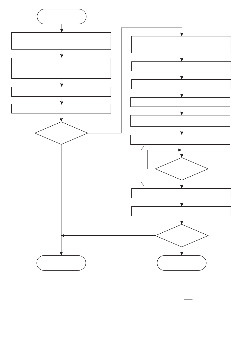
4-Level FSK Modem Data Pump Page 31 of 47 MX919B PRELIMINARY INFORMATION
©2001 MX•COM, INC. www.mxcom.com Tele: 800 638 5577 336 744 5050 Fax: 336 744 5054 Doc. # 20480170.003
4800 Bethania Station Road, Winston-Salem, NC 27105-1201 USA All trademarks and service marks are held by their respective companies.
Note: during this time the µC may
perform other functions, as the
µC variable 'STATE' is updated
by the interrupt service routine
Disable µC's MX919B Tx Interrupt Service Routine
Enable µC's MX919B Tx Interrupt Service Routine
Set µC variable 'STATE' to 0
Set the Mode Register IRQEN bit to '1'
Set the Mode Register IRQEN bit to '0'
Read the Status Register
Write a RESET task to the Command Register
Set µC variable 'IBLOCKS'
to the number of Intermediate blocks
to be transmitted
Ensure that the Control Register
has been loaded with
a suitable CKDIV value
Write a T24S task to the Command Register
Write 6 bytes of Symbol Sync
pattern to the Data Buffer
Ensure that the Mode Register
IRQEN, PSAVE and RXEYE bits are '0',
the TX/RX bit is '1',
and the INVSYM bit is set appropriately
Ye s
Ye s
Ye s
No
No
No
END
with error END
START
'STATE' < 5 ?
BFREE bit = 1 ?
'STATE' = 5 ?
Figure 19: Transmit Frame Example Flowchart, Main Program
Notes
1. The RESET command in Figure 19 and the practice of disabling the MX919B’s IRQ output when not
needed are not essential but can eliminate problems during debugging and if errors occur in operation
2. The CRC and TXIMP bits should be set appropriately every time a byte is written to the Command
Register.
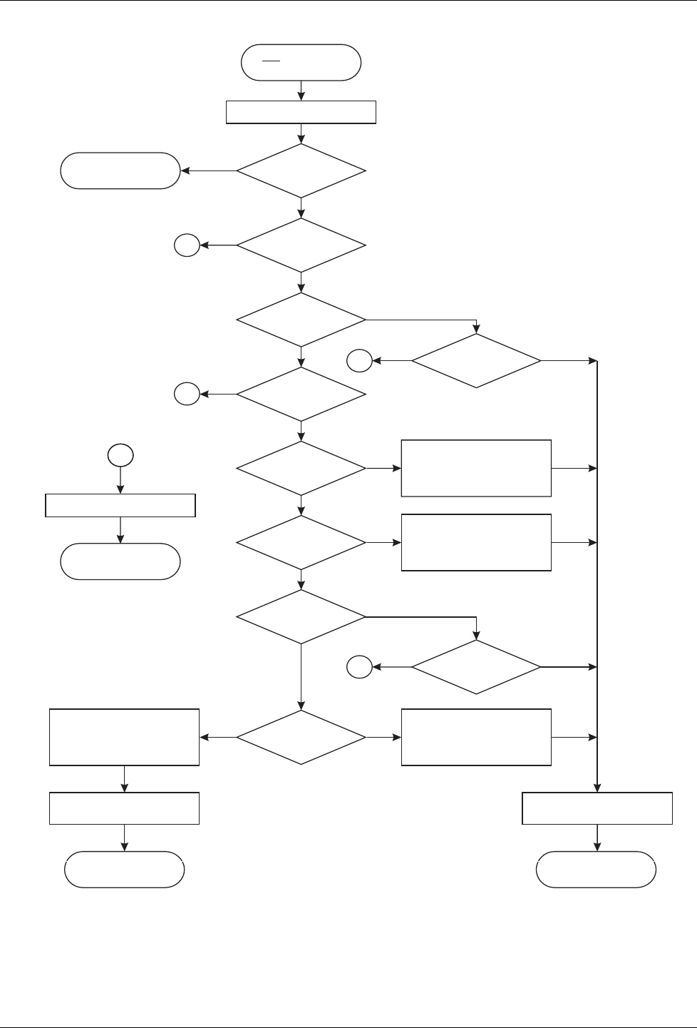
4-Level FSK Modem Data Pump Page 32 of 47 MX919B PRELIMINARY INFORMATION
©2001 MX•COM, INC. www.mxcom.com Tele: 800 638 5577 336 744 5050 Fax: 336 744 5054 Doc. # 20480170.003
4800 Bethania Station Road, Winston-Salem, NC 27105-1201 USA All trademarks and service marks are held by their respective companies.
.
Ye s
No
RETURN
RETURN
'STATE' = 3 ?
Set µC variable 'STATE' to 9
RETURN
( Error )
E
Decrement µC variable
'IBLOCKS'
Write 8 Last Block
data bytes to the Data Buffer
then write a TLB task to
the Command Register
Write 6 byte Frame Sync
pattern to the Data Buffer
then write a T24S task to
the Command Register
Write 10 Header Block
data bytes to the Data Buffer
then write a THB task to
the Command Register
Increment µC variable
'STATE'
Read Status Register
Ye s
Ye s
No
No
No
Ye s
No
START
( line goes low )IRQ
RETURN
( Not MX919B IRQ ) IRQ bit = 1 ?
BFREE bit = 1 ?
'STATE' = 4 ?
'IBLOCKS' = 0 ?
'STATE' = 1 ?
Ye s
IBEMPTY bit = 1 ?
Ye s
No
'STATE' = 2 ?
No
Ye s
'STATE' = 0 ?
IBEMPTY bit = 1 ?
Write 12 Intermediate Block
data bytes to the Data Buffer
then write a TIB task to
the Command Register
E
No
E
Ye s
E
E
No
No
Ye s
Ye s
Value of C variable 'STATE' on entry to IRQ routine
and corresponding MX919B's actions:
0: Symbol Sync pattern being transmitted,
load Frame Sync pattern & T24S task.
1: Frame Sync pattern being transmitted,
load Header Block bytes and THB task.
2: Header or Intermmediate Block being transmitted,
load Intermediate or Last Block bytes & TIB or TLB task.
3: Last block being transmitted,
ignore this interrupt.
4: Waiting for end of transmission,
finish on interrupt with IBEMPTY bit set.
µ
Figure 20: Tx Interrupt Service Routine

4-Level FSK Modem Data Pump Page 33 of 47 MX919B PRELIMINARY INFORMATION
©2001 MX•COM, INC. www.mxcom.com Tele: 800 638 5577 336 744 5050 Fax: 336 744 5054 Doc. # 20480170.003
4800 Bethania Station Road, Winston-Salem, NC 27105-1201 USA All trademarks and service marks are held by their respective companies.
5.2 Receive Frame Example
The operations needed to receive a single Frame consisting of Symbol and Frame Sync sequences and one
each Header, Intermediate and Last blocks are shown below;
1. Ensure that the Control Register has been loaded with suitable CKDIV, FSTOL, LEVRES and PLLBW
values, and that the IRQEN bit of the Mode Register is '1', the TX RX/ PSAVE, and RXEYE bits are '0',
and the INVSYM bit is set appropriately.
2. Wait until the received carrier has been present for at least 8 symbol times (see Section 5.3).
3. Read the Status Register to ensure that the BFREE bit is '1'.
4. Write a byte containing a SFSH task and with the AQSC and AQLEV bits set to '1' to the Command
Register.
5. Wait for an interrupt from the modem, read the Status Register; the IRQ and BFREE bits should be '1'
and the CRCERR and DIBOVF bits should be '0'.
6. Check that the CRCERR bit of the Status Register is '0' and read 10 Header Block bytes from the Data
Block Buffer.
7. Write a RILB task to the Command Register.
8. Wait for an interrupt from the modem, read the Status Register; the IRQ and BFREE bits should be '1'
and the DIBOVF bit '0'.
9. Read 12 Intermediate Block bytes from the Data Block Buffer.
10. Write a RILB task to the Command Register.
11. Wait for an interrupt from the modem, read the Status Register; the IRQ and BFREE bits should be '1'
and the DIBOVF bit '0'.
12. Check that the CRCERR bit of the Status Register is '0' and read the 8 Last Block bytes from Data
Buffer.
Figure 21 and Figure 22 illustrate the host µC routines needed to receive a single Frame consisting of Symbol
and Frame Sync patterns, a Header Block, any number of Intermediate blocks and one Last block. It is
assumed that the Rx Interrupt Service Routine Figure 22 is called when the MX919B’s IRQ output goes low.
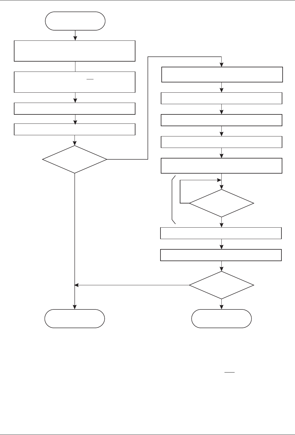
4-Level FSK Modem Data Pump Page 34 of 47 MX919B PRELIMINARY INFORMATION
©2001 MX•COM, INC. www.mxcom.com Tele: 800 638 5577 336 744 5050 Fax: 336 744 5054 Doc. # 20480170.003
4800 Bethania Station Road, Winston-Salem, NC 27105-1201 USA All trademarks and service marks are held by their respective companies.
Note: during this time the µC may
perform other functions, as the
µC variable 'STATE' is updated
by the interrupt service routine
Disable µC's MX919B Rx Interrupt Service Routine
Enable µC's MX919B Rx Interrupt Service Routine
Set µC variable 'STATE' to 0
Set the Mode Register IRQEN bit to '1'
Set the Mode Register IRQEN bit to '0'
Read the Status Register
Write a RESET task to the Command Register
Ensure that the Control Register
has been loaded with suitable
CKDIV, FSTOL, LEVRES and PLLBW values
Wait until the received carrier has been present
for at least 8 symbol times
Write a SFSH task to the Command Register
with the AQSC and AQLEV bits set to '1'
Ensure that the Mode Register IRQEN,
PSAVE, RXEYE and TX/RX bits are '0',
and the INVSYM bit is set appropriately
Ye s
Ye s
Ye s
No
No
No
END
with error END
START
'STATE' < 3 ?
BFREE bit = 1 ?
'STATE' = 3 ?
Figure 21: Receive Frame Example Flowchart, Main Program
Notes
1. The RESET command in Figure 21 and the practice of disabling the MX919B’s IRQ output when not
needed are not essential but can eliminate problems during debugging and if errors occur in operation.
2. The CRC and TXIMP bits should be set appropriately every time a byte is written to the Command
Register.
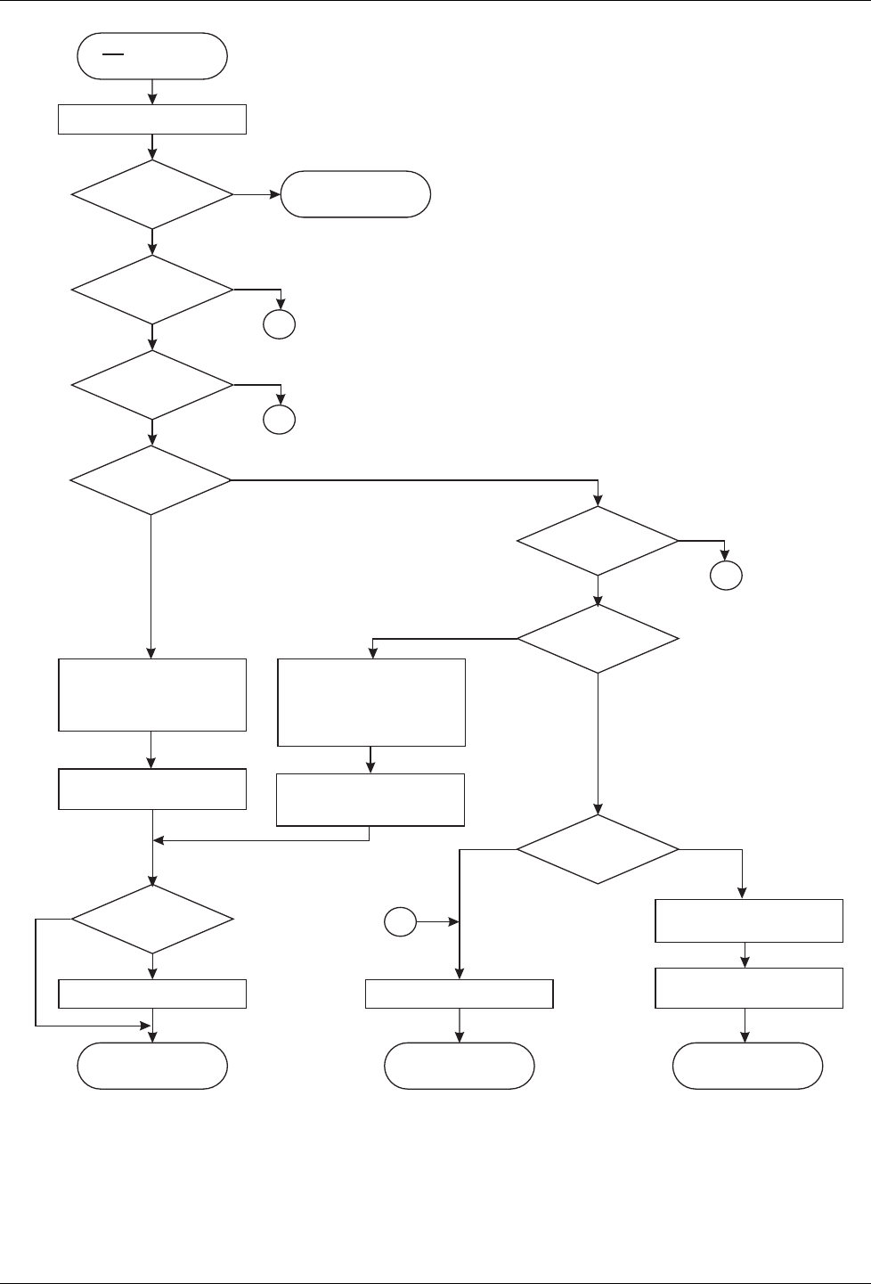
4-Level FSK Modem Data Pump Page 35 of 47 MX919B PRELIMINARY INFORMATION
©2001 MX•COM, INC. www.mxcom.com Tele: 800 638 5577 336 744 5050 Fax: 336 744 5054 Doc. # 20480170.003
4800 Bethania Station Road, Winston-Salem, NC 27105-1201 USA All trademarks and service marks are held by their respective companies.
Value of µC variable 'STATE' on entry to IRQ routine
and corresponding MX919B's actions:
0 : Frame Sync has been recognized
and Header block received,
read out data and load RILB task.
1 : Intermediate block has been received,
read out data and load RILB task.
2 : Last block has been received,
read out data and finish.
Read Status Register
Ye s
Ye s
Ye s
Ye s
Ye s
Ye s
Ye s
Ye s
No
No
No
No
No
No
No
No
START
( line goes low )IRQ
RETURNRETURN
RETURN
( Not MX919B IRQ )
IRQ bit = 1 ?
BFREE bit = 1 ?
DIBOVF bit = 0 ?
'STATE' = 0 ?
'STATE' = 1 ?
CRCERR bit = 0 ?
'IBLOCKS' = 0 ?
'STATE' = 2 ?
E
E
E
Set µC variable 'STATE' to 9Set µC variable 'STATE' to 2
Decrement µC variable
'IBLOCKS'
RETURN
( Error )
E
Read 10 Header block bytes
from the Data Buffer then
write a RILB task to the
Command Register
SEE NOTE BELOW
Read 12 Intermediate Block
bytes from the Data Buffer
then write a RILB task to
the Command Register
Set µC variable 'IBLOCKS'
to the number of Intermediate
Blocks to be received
Read 8 Last Block data bytes
from the Data Buffer.
Increment µC variable
'STATE'
Figure 22: Rx Interrupt Service routine
Note: This routine assumes that the number of Intermediate blocks in the Frame is contained within the
Header Block Data.
4-Level FSK Modem Data Pump Page 36 of 47 MX919B PRELIMINARY INFORMATION
©2001 MX•COM, INC. www.mxcom.com Tele: 800 638 5577 336 744 5050 Fax: 336 744 5054 Doc. # 20480170.003
4800 Bethania Station Road, Winston-Salem, NC 27105-1201 USA All trademarks and service marks are held by their respective companies.
5.3 Clock Extraction and Level Measurement Systems
5.3.1 Supported Types of Systems
The MX919B is intended for use in systems where:
1. The Symbol Sync pattern is transmitted immediately on start-up of the transmitter, before the first Frame
Sync pattern (see Figure 23).
2. A terminal may remain powered up indefinitely, transmitting concatenated Frames with or without
intervening Symbol Sync patterns (each Frame having a Frame Sync pattern and symbol timing being
maintained from one Frame to the next).
3. A receiving modem may be switched onto a channel before the distant transmitter has started up, or may
be switched onto a channel where the transmitting station is already sending concatenated Frames
5.3.2 Clock and Level Acquisition Procedures with RF Carrier Detect
When the receiving modem is enabled or switched onto a channel, it needs to establish the received symbol
levels, clock timing, and look for a Frame Sync pattern in the incoming signal. This is best done by the
following procedure:
1. Ensure that the Control Register's PLLBW bits are set to 'Wide' and the LEVRES bits to 'Track'.
2. Wait until a received carrier has been present for 8 symbol times. This 8-symbol delay gives time for the
received signal to propagate through the modem's RRC filter. An 'RF received 8 symbol times' qualifying
function can be included in a radio's carrier detect circuitry to take this into account.
3. Write a SFS or SFSH task to the Command Register with the AQSC and the AQLEV bits set to '1'.
4. When the modem interrupts to signal that it has recognized a Frame Sync pattern (or completed the
SFSH task) then change the PLLBW bits to 'Medium'.
Once the receiving modem has achieved level and symbol timing synchronization with a particular channel -
as evidenced by recognition of a Frame Sync pattern - then subsequent concatenated Frames can be read by
simply issuing SFS or SFSH tasks at appropriate times, keeping the ASQSC and AQLEV bits at zero, and the
PLLBW and LEVRES bits at their current 'Medium' and 'Track' settings, respectively.
Rx Signal from
FM discriminator
to Modem
Noise Frame Sync Rest of Frame
Set AQSC and AQLEV bits
to start Acquisition sequences
Level Measurement and Clock
Extraction Circuits
Increasing accuracy and lengthening response times
8-Symbol delay determined by external
circuit such as RF carrier detect
Symbol Sync
Figure 23: Acquisition Sequence Timing
5.3.3 Clock and Level Acquisition Procedure without RF Carrier Detect
It is also possible to use the modem in a system where there is an indeterminate delay between the RF
transmitter turn on time and the transmission moment of the Symbol Sync pattern, or where a receive carrier
detect signal is not available to the controlling µC, or where the transmitting terminal can send separate
unsynchronized Frames. In these cases, each Frame should be preceded by, a Symbol Sync pattern which
should be extended to about 100 symbols and the procedure provided in Section 5.3.2. used.
4-Level FSK Modem Data Pump Page 37 of 47 MX919B PRELIMINARY INFORMATION
©2001 MX•COM, INC. www.mxcom.com Tele: 800 638 5577 336 744 5050 Fax: 336 744 5054 Doc. # 20480170.003
4800 Bethania Station Road, Winston-Salem, NC 27105-1201 USA All trademarks and service marks are held by their respective companies.
5.3.4 Automatic Acquisition Functions
Setting the AQSC and AQLEV bits to '1' triggers the modem's automatic Symbol Clock Extraction and Level
Measurement acquisition sequences, which are designed to measure the received symbol timing, amplitude,
and DC offset as quickly as possible before switching to accurate - but slower - measurement modes. These
acquisition sequences act very quickly if triggered at the start of a received Symbol Sync pattern (as shown in
Figure 23), but will still function correctly, although more slowly, if started any time during a normal Frame as
when the receiver is switched onto a channel where the transmitter is operating continuously.
The automatic AQLEV Level Measurement acquisition sequence starts with the level measurement circuits
being put into 'Clamp' Mode for one symbol time to quickly set the voltages on the DOC pins to approximately
correct levels. The level measurement circuits are then automatically set to 'Lossy Peak Detect' mode for 15
symbol times, then 'Slow Peak Detect' until a received Frame Sync pattern is recognized, after which the
automatic sequence ends and the level measurement circuit mode reverts to the mode set by the LEVRES
bits of the Control Register (normally 'Level Track').
The peak detectors used in both 'Slow' and 'Lossy Peak Detect' modes include additional low pass filtering of
the received signal which greatly reduces the effect of pattern noise on the reference voltages held on the
external DOC capacitors, but means that pairs of '+3' (and '-3') symbols need to be received to establish the
correct levels. Two pairs of '+3' and two pairs of '-3' symbols received after the start of an AQLEV sequence
are sufficient to correctly set the levels on the DOC capacitors.
The automatic AQSC Symbol Clock acquisition sequence sets the PLL to 'Extra Wide Bandwidth' mode for 16
symbol times (this mode is not one of those which can be selected by the Control Register PLLBW bits) then
changes to 'Wide' bandwidth. After 45 symbol times, the PLL mode will revert to that set by the Control
Register PLLBW bits.
5.4 AC Coupling
For a practical circuit, ac coupling between the modem's transmit output to the frequency modulator and
between the receiver's frequency discriminator and the receive input of the modem may be desired. There
are, however, two issues which deserve consideration:
1. AC coupling of the signal degrades the Bit Error Rate performance of the modem. The following graph
illustrates the typical bit error rates at 4800 symbols/sec (9600bps) without FEC for reasonably random data
with differing degrees of AC coupling:
1.E-04
1.E-03
1.E-02
1.E-01
4567891011121314
S/N dB (Noise in 20 to 9600Hz band)
BER
Tx 5Hz, RxDC
Tx 5Hz, Rx10Hz
Tx & Rx DC coupled
Tx 5Hz, Rx5Hz
Figure 24: Effect of AC Coupling on BER (without FEC)

4-Level FSK Modem Data Pump Page 38 of 47 MX919B PRELIMINARY INFORMATION
©2001 MX•COM, INC. www.mxcom.com Tele: 800 638 5577 336 744 5050 Fax: 336 744 5054 Doc. # 20480170.003
4800 Bethania Station Road, Winston-Salem, NC 27105-1201 USA All trademarks and service marks are held by their respective companies.
2. Any ac coupling at the receive input will transform any step in the voltage at the discriminator output to a
slowly decaying pulse which can confuse the modem's level measuring circuits. As illustrated in Figure 25
below, the time for this step to decay to 37% of its original value is 'RC' where:
network) RC the offrequency off-cut (3dB2
1
=RC π
which is 32ms, or 153 symbol times at 4800 symbols/sec (9600bps) for a 5Hz network.
37%
T = RC
100%
Step Input
to RC Circuit
Output of
RC Circuit
Figure 25: Decay Time - AC Coupling
In general, it is best to DC couple the receiver discriminator to the modem and ensure that any AC coupling to
the transmitter's frequency modulator has a -3dB cut-off frequency of no higher than 5Hz for 4800
symbols/sec (9600bps).
4-Level FSK Modem Data Pump Page 39 of 47 MX919B PRELIMINARY INFORMATION
©2001 MX•COM, INC. www.mxcom.com Tele: 800 638 5577 336 744 5050 Fax: 336 744 5054 Doc. # 20480170.003
4800 Bethania Station Road, Winston-Salem, NC 27105-1201 USA All trademarks and service marks are held by their respective companies.
5.5 Radio Performance
The maximum data rate that can be transmitted over a radio channel using these modems depends on:
• RF channel spacing.
• Allowable adjacent channel interference.
• Symbol rate.
• Peak carrier deviation (modulation index).
• Tx and Rx reference oscillator accuracy.
• Modulator and demodulator linearity.
• Receiver IF filter frequency and phase characteristics.
• Use of error correction techniques.
• Acceptable error rate.
As a guide, 4800 symbols/sec (9600bps) can be achieved (subject to local regulatory requirements) over a
system with 12.5kHz channel spacing if the transmitter frequency deviation is set to ±2.5kHz peak for a
repetitive ' +3 +3 -3 -3 ... ' pattern and the maximum difference between transmitter and receiver 'carrier'
frequencies is less than 2400Hz.
The modulation scheme employed by these modems is designed to achieve high data throughput by
exploiting as much as possible of the RF channel bandwidth. However; this does place constraints on the
performance of the radio. Particular attention must be paid to:
• Linearity, frequency, and phase response of the Tx Frequency Modulator. For a 4800 symbols/sec
(9600bps) system, the frequency response should be within ±2dB over the range 3Hz to 5kHz, relative to
2400Hz.
• The bandwidth and phase response of the receiver's IF filters.
• Accuracy of the Tx and Rx reference oscillators, as any difference will shift the received signal towards
the skirts of the IF filter response and cause a DC offset at the discriminator output.
Viewing the equalized received signal eye diagram, using the Mode Register RXEYE function, provides a
good indication of the overall RF transmitter/receiver performance.
Rx
CIRCUITS
Tx
CIRCUITS
D0 - D7
A0 - A1
CS
RD
WR
IRQ
D0 - D7
A0 - A1
CS
RD
WR
IRQ
TXOUT
SIGNAL AND
DC LEVEL
ADJUSTMENT
SIGNAL LEVEL
ADJUSTMENT
RXIN RXAMPOUT
Rx FREQUENCY
DISCRIMINATOR
Tx FREQUENCY
MODULATOR
DC LEVEL
ADJUSTMENT
MX919B MODEM
µC
µC
Figure 26: Typical Connections between Radio and MX919B
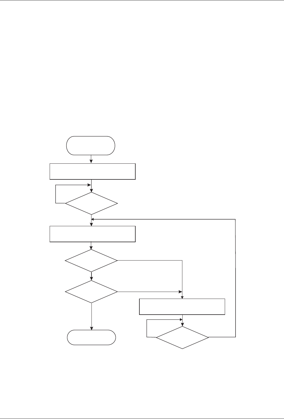
4-Level FSK Modem Data Pump Page 40 of 47 MX919B PRELIMINARY INFORMATION
©2001 MX•COM, INC. www.mxcom.com Tele: 800 638 5577 336 744 5050 Fax: 336 744 5054 Doc. # 20480170.003
4800 Bethania Station Road, Winston-Salem, NC 27105-1201 USA All trademarks and service marks are held by their respective companies.
5.6 Received Signal Quality Monitor
In applications where the modem has to monitor a long transmission containing a number of concatenated
Frames, it is recommended that the controlling software include a function which regularly checks that the
modem is still receiving a good data signal and triggers a re-acquisition and possibly changes to another
channel if a problem is encountered. This strategy has been shown to improve the system's overall
performance in situation where fading, large noise bursts, severe co-channel interference, or loss of the
received signal for long periods are likely to occur.
Such a function can be simply implemented by regularly reading the Data Quality Register, which gives a
measure of the overall quality of the received signal, as well as the current effectiveness of the modem's clock
extraction and level measurement systems. Experience has shown that if two consecutive DQ readings are
both less than 50 then it is worth instructing the MX919B to re-acquire the received signal levels and timing
once it has been established that the received carrier level is satisfactory. Re-acquisition should follow the
procedure given in Section 5.3.
The intervals between Data Quality readings is not critical, but should be a minimum of 64 symbol times
except for the first reading made after triggering the AQSC and AQLEV automatic acquisition sequences,
which should be delayed for about 250 symbol times.
A suitable algorithm is shown in Figure 27.
Note: Times are symbol times.
Reset timer.
Set µC variable 'LAST_DQ' to 99
Read DQ register into
µC variable 'THIS_DQ'
Copy 'THIS_DQ' to 'LAST DQ'.
Reset Timer.
Ye s
Ye s
Ye s
No
No
No
No
AQSC/AQLEV
task issued
Re Acquire
Timer > 250 ?
Timer > 64 ?
'THIS_DQ' < 50 ?
'LAST_DQ' < 50 ?
Figure 27: Received Signal Quality Monitor Flowchart

4-Level FSK Modem Data Pump Page 41 of 47 MX919B PRELIMINARY INFORMATION
©2001 MX•COM, INC. www.mxcom.com Tele: 800 638 5577 336 744 5050 Fax: 336 744 5054 Doc. # 20480170.003
4800 Bethania Station Road, Winston-Salem, NC 27105-1201 USA All trademarks and service marks are held by their respective companies.
6. Performance Specification
6.1 Electrical Performance
6.1.1 Absolute Maximum Ratings
Exceeding these maximum ratings can result in damage to the device.
General Min. Max. Units
Supply (VDD – VSS) -0.3 7.0 V
Voltage on any pin to VSS -0.3 VDD + 0.3 V
Current
VDD -30 30 mA
VSS -30 30 mA
Any other pin -20 20 mA
DW, LH, P Package
Total Allowable Power Dissipation at TAMB = 25°C 800 mW
Derating above 25°C 13 mW/°C above 25°C
Storage Temperature -55 125 °C
Operating Temperature -40 85 °C
DS Package
Total Allowable Power Dissipation at TAMB = 25°C 550 mW
Derating above 25°C 9 mW/°C above 25°C
Storage Temperature -55 125 °C
Operating Temperature -40 85 °C
6.1.2 Operating Limits
Correct operation of the device outside these limits is not implied.
Notes Min. Max. Units
Supply (VDD – VSS) 3.0 5.5 V
Symbol Rate 2400 9600 Symbols/sec
Temperature -40 85 °C
Xtal Frequency 1.0 10.0 MHz

4-Level FSK Modem Data Pump Page 42 of 47 MX919B PRELIMINARY INFORMATION
©2001 MX•COM, INC. www.mxcom.com Tele: 800 638 5577 336 744 5050 Fax: 336 744 5054 Doc. # 20480170.003
4800 Bethania Station Road, Winston-Salem, NC 27105-1201 USA All trademarks and service marks are held by their respective companies.
6.1.3 Operating Characteristics
For the following conditions unless otherwise specified:
Xtal Frequency = 4.9152MHz, Symbol Rate = 4800 symbols/sec,
Noise Bandwidth = 0 to 9600Hz, VDD = 5.0V @ TAMB = 25°C
Notes Min. Typ. Max. Units
DC Parameters
IDD 1 4.0 10.0 mA
IDD (VDD = 3.3V) 1 2.5 6.3 mA
IDD (Powersave Mode) 1 1.5 mA
IDD (Powersave Mode, VDD = 3.3V) 1 0.6 mA
AC Parameters
TX Output
TXOUT Impedance 2 1.0 2.5 kΩ
Signal Level
TXIMP = 0 3 0.8 1.0 1.2 VP-P
TXIMP = 1 3 0.88 1.1 1.32 VP-P
Output DC Offset with respect to VDD/2 4 -0.25 0.25 V
RX Input
RXIN Impedance (at 100Hz) 10.0 MΩ
RXIN Amp Voltage Gain (input = 1mVRMS at 100Hz) 300 V/V
Input Signal Level 5 0.7 1.0 1.3 VP-P
DC Offset with respect to VDD/2 5 -0.5 0.5 V
XTAL/CLOCK INPUT
‘High’ Pulse Width 6 40 ns
‘Low’ Pulse Width 6 40 ns
Input Impedance (at 100Hz) 10.0 MΩ
Inverter Gain (input = 1mVRMS at 100Hz) 20 dB
µC Interface
Input Logic ‘1’ Level 7,8 70% VDD
Input Logic ‘0’ Level 7,8 30% VDD
Input Leakage Current (VIN = 0 to VDD) 7,8 -5.0 5.0 µA
Input Capacitance 7,8 10.0 pF
Output Logic ‘1’ Level (IOH = 120µA) 8 92% VDD
Output Logic ‘0’ Level (IOL = 360µA) 8,9 8% VDD
‘Off’ State Leakage Current (VOUT = VDD) 9 10 µA
6.1.3.1 Operating Characteristics Notes:
1. Not including any current drawn from the modem pins by external circuitry other than the Xtal oscillator.
2. Small signal impedance.
3. Measured after the external RC filter (R4/C5) for a "+3 +3 -3 -3...." symbol sequence, (Tx output level is
proportional to VDD).
4. Measured at the TXOUT pin with the modem in the Tx idle mode.
5. For optimum performance, measured at RXAMPOUT pin, for a "...+3 +3 -3 -3..." symbol sequence,
TXIMP = 0 or 1, The optimum level and DC offset values are proportional to VDD.
6. Timing for an external input to the XTAL/CLOCK pin.
7. WR , RD , CS , A0 and A1 pins.
8. D0 - D7 pins.
9. IRQ pin.

4-Level FSK Modem Data Pump Page 43 of 47 MX919B PRELIMINARY INFORMATION
©2001 MX•COM, INC. www.mxcom.com Tele: 800 638 5577 336 744 5050 Fax: 336 744 5054 Doc. # 20480170.003
4800 Bethania Station Road, Winston-Salem, NC 27105-1201 USA All trademarks and service marks are held by their respective companies.
6.1.4 Timing
µC Parallel Interface Timings (see Figure 28 ) Notes Min. Typ. Max. Units
tACSL Address valid to CS low time 0 ns
tAH Address hold time 0 ns
tCSH CS hold time 0 ns
tCSHI CS high time 1 6 clock cycles
tCSRWL CS to WR or RD low time 0 ns
tDHR Read data hold time 0 ns
tDHW Write data hold time 0 ns
tDSW Write data setup time 90 ns
tRHCSL RD high to CS low time (write) 0 ns
tRACL Read access time from CS low 2 175 ns
tRARL Read access time from RD low 2 145 ns
tRL RD low time 200 ns
tRX RD high to D0-D7 3 state time 50 ns
tWHCSL WR high to CS low time (read) 0 ns
tWL WR low time 200 ns
Timing Notes:
1. Xtal/Clock cycles at the XTAL/CLOCK pin.
2. With 30pF max to VSS on D0 - D7 pins.
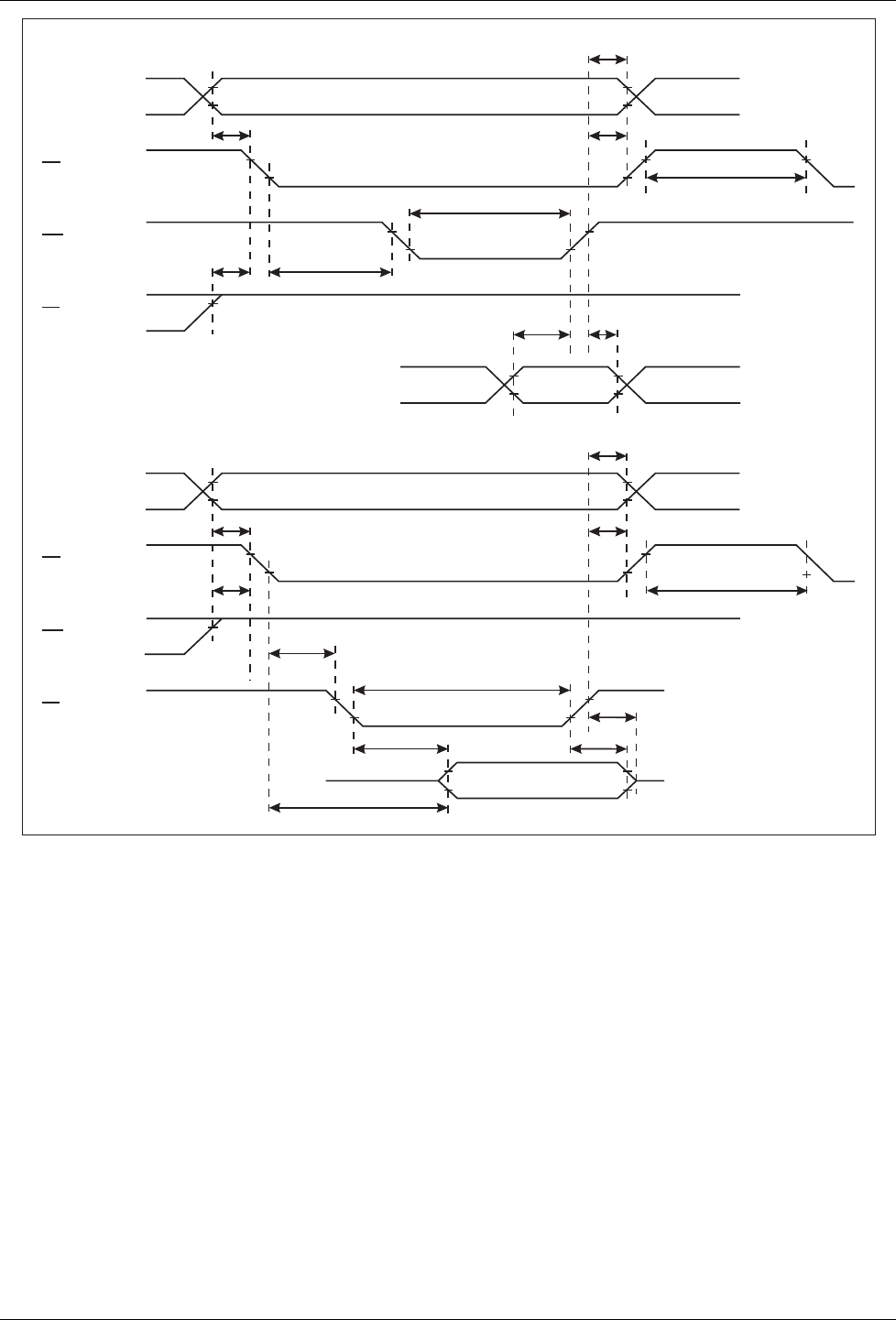
4-Level FSK Modem Data Pump Page 44 of 47 MX919B PRELIMINARY INFORMATION
©2001 MX•COM, INC. www.mxcom.com Tele: 800 638 5577 336 744 5050 Fax: 336 744 5054 Doc. # 20480170.003
4800 Bethania Station Road, Winston-Salem, NC 27105-1201 USA All trademarks and service marks are held by their respective companies.
DATA
D0 to D7 (1 byte)
READ CYCLE (DATA FROM MODEM)
ADDRESS VALID
DATA
D0 to D7 (1 byte)
t
RL
t
DHR
t
RX
DATA VALID
DATA
VALID
WRITE CYCLE (DATA TO MODEM)
t
CSRWL
t
RHCSL
t
DSW
t
DHW
t
WHCSL
t
RARL
t
RACL
ADDRESS
A0 A1
,
t
AH
t
ACSL
t
CSRWL
t
WL
t
CSHI
t
CSH
t
AH
t
ACSL
t
CSHI
t
CSH
ADDRESS VALID
CS
WR
RD
ADDRESS
A0 A1
,
CS
WR
RD
Figure 28: µ
µµ
µC Parallel Interface Timings
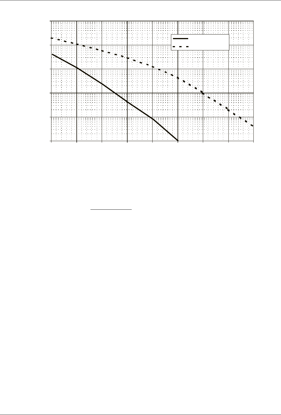
4-Level FSK Modem Data Pump Page 45 of 47 MX919B PRELIMINARY INFORMATION
©2001 MX•COM, INC. www.mxcom.com Tele: 800 638 5577 336 744 5050 Fax: 336 744 5054 Doc. # 20480170.003
4800 Bethania Station Road, Winston-Salem, NC 27105-1201 USA All trademarks and service marks are held by their respective companies.
6.1.5 Typical Bit Error Rate
1E-6
1E-5
1E-4
1E-3
1E-2
1E-1
8 9 10 11 12 13 14 15 16
S/N dB (Noise in 2 x Symbol RateBandwidth)
BER
BER with FEC
BER without FEC
Figure 29: Typical Bit Error Rate With and Without FEC
Measured under nominal working conditions, LEVRES bits set to 'Level Track' or 'Slow Peak Detect' and
PLLBW bits set to 'Medium' or 'Narrow' Bandwidth, Command Register TXIMP bit set to '0' or '1' (same for Tx
and Rx devices), with pseudo-random data.
Note: )
Noise Voltage
Voltage Signal
(20log as calculates N/S 10
Where: Signal Voltage is the measured VRMS of a random 4-level signal.
Noise Voltage is the VRMS of a flat Gaussian noise signal having a bandwidth from a few Hz to
twice the symbol rate e.g. to 9600Hz when measuring a 4800 symbol/sec (9600bps) system.
Both signals are measured at the same point in the test circuit.
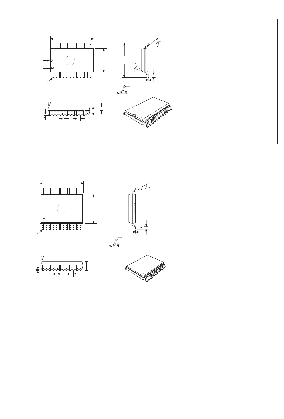
4-Level FSK Modem Data Pump Page 46 of 47 MX919B PRELIMINARY INFORMATION
©2001 MX•COM, INC. www.mxcom.com Tele: 800 638 5577 336 744 5050 Fax: 336 744 5054 Doc. # 20480170.003
4800 Bethania Station Road, Winston-Salem, NC 27105-1201 USA All trademarks and service marks are held by their respective companies.
6.2 Packaging
0.597 (15.16)
Package Tolerances
A
B
C
E
H
TYP. MAX.MIN.DIM.
J
P
X
W
T
Y
K
L
0.105 (2.67)
0.093 (2.36)
0.419 (10.64)
45°
7°
0° 10°
0.050 (1.27)
0.046 (1.17)
0.613 (15.57)
0.299 (7.59)
0.050 (1.27)
0.016 (0.41)
0.390 (9.90)
0.020 (0.51)0.003 (0.08)
0.009 (0.23) 0.0125 (0.32)
0.013 (0.33) 0.020 (0.51)
0.036 (0.91)
0.286 (7.26)
Z
NOTE : All dimensions in inches (mm.)
Angles are in degrees
5°
5°
PIN 1
A
B
ALTERNATIVE
PIN
LOCATION
MARKING
X
P
J
Y
C
H
K
E
L
T
W
Z
Figure 30: 24-pin SOIC Mechanical Outline: Order as part no. MX919BDW
NOTE : All dimensions in inches (mm.)
Angles are in degrees
Package Tolerances
A
B
C
E
H
TYP. MAX.MIN.
DIM.
J
P
X
T
Y
Z
L
0.079 (2.00)0.066 (1.67)
0.312 (7.90)
0°
7°
4°
8°
9°
10°
0.037 (0.95)
0.328 (8.33)
0.213 (5.39)
0.026 (0.65)
0.022 (0.55)
0.301 (7.65)
0.008 (0.21)0.002 (0.05)
0.005 (0.13) 0.009 (0.22)
0.010 (0.25) 0.015 (0.38)
0.318 (8.07)
0.205 (5.20)
X
C
H
P
J
Y
E
Z
L
T
PIN 1
PIN 1
A
B
Figure 31: 24-pin SSOP Mechanical Outline: Order as part no. MX919BDS
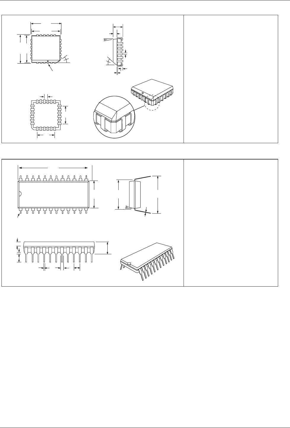
4-Level FSK Modem Data Pump Page 47 of 47 MX919B PRELIMINARY INFORMATION
©2001 MX•COM, INC. www.mxcom.com Tele: 800 638 5577 336 744 5050 Fax: 336 744 5054 Doc. # 20480170.003
4800 Bethania Station Road, Winston-Salem, NC 27105-1201 USA All trademarks and service marks are held by their respective companies.
Package Tolerances
NOTE : All dimensions in inches (mm.)
Angles are in degrees
A
B
C
D
E
H
P
F
G
TYP. MAX.MIN.DIM.
K
J
W
T
Y
0.435 (11.05)
0.435 (11.05)
0.051 (1.30)
0.009 (0.22)
6°
30°
0.409 (10.40)
0.409 (10.40)
0.146 (3.70)
0.417 (10.60)
0.417 (10.60)
0.049 (1.24)
0.006 (0.152)
0.250 (6.35)
0.250 (6.35)
0.023 (0.58)
0.047 (1.19)
0.022 (0.55)0.018 (0.45)
0.380 (9.61)
0.380 (9.61)
0.128 (3.25)
0.048 (1.22)
45°
F
G
P
A
D
B
E
PIN 1
W
C
J
K
Y
W
H
T
Figure 32: 24-pin PLCC Mechanical Outline : Order as part no. MX919BLH
NOTE : All dimensions in inches (mm.)
Angles are in degrees
Package Tolerances
A
B
C
E
E1
H
TYP. MAX.MIN.DIM.
J
J1
P
Y
T
K
L
0.220 (5.59)
0.555 (14.04)
0.670 (17.02)
7°
0.160 (4.05)
1.270 (32.26)
0.151 (3.84)
0.100 (2.54)
0.121 (3.07)
0.600 (15.24)
0.590 (14.99) 0.625 (15.88)
0.015 (0.38) 0.045 (1.14)
0.008 (0.20) 0.015 (0.38)
0.015 (0.38) 0.023 (0.58)
0.040 (1.02) 0.065 (1.65)
0.066 (1.67) 0.074 (1.88)
1.200 (30.48)
0.500 (12.70)
H
K
L
J1
JP
C
B
A
PIN1 T
E
E1
Y
Figure 33: 24-pin PDIP Mechanical Outline: Order as part no. MX919BP