IP Mobilenet IPMNIP8 IP8HPV Data Transceiver User Manual IP8HPV FCCRpt
IP Mobilenet, LLC IP8HPV Data Transceiver IP8HPV FCCRpt
Contents
Manual

I
IN
NV
VA
AD
DR
Rt
tm
m
I
IP
P8
8H
HP
PV
V
D
Da
at
ta
a
T
Tr
ra
an
ns
sc
ce
ei
iv
ve
er
r
Owner’s Manual
Date Prepared:
October 25, 2001
Document Control #: DC-39
Version: C-1 (Special Release)
Copyright 2001 IPMobileNet, Inc.
11909 East Telegraph Road Santa Fe Springs, CA 90670-3785
Voice: (562) 946-9493 Fax: (562) 949-0223

TABLE OF CONTENTS
~\Technical Documentation\System Manuals\FCC-Reports\IP8HPV\IP8HPV-FCCRpt.doc Page 2
SECTION 1: THEORY OF OPERATION ................................................................................. 3
General Block Diagram................................................................................................ 3
General Block Diagram Definitions..................................................................... 3
Microcontroller.................................................................................................... 5
Support Circuitry ................................................................................... 5
Input/Output........................................................................................................ 5
Injection Synthesizer .......................................................................................... 6
Transmitter/TR Switch........................................................................................ 6
Receiver 1 Front-End ......................................................................................... 6
Receiver 1 IF ...................................................................................................... 7
Transmit Modulation........................................................................................... 7
Baseband Routing.............................................................................................. 7
Power and Analog Ground ................................................................................. 8
Receiver 2 Front-End ......................................................................................... 8
Receiver 2 IF ...................................................................................................... 8
Modem .............................................................................................................. 9
VLogic and Digital Ground ................................................................................. 9
SECTION 2: FACTORY TEST PROCEDURE ....................................................................... 10
Equipment List ........................................................................................................... 10
Programming and Configuring Mobile Radio.......................................................... 11
Adjustment / Alignment Procedures ........................................................................ 12
Receiver Injection............................................................................................. 12
Receiver 1
........................................................................................................ 12
Receiver 2
........................................................................................................ 13
Transmit Data................................................................................................... 14
Transmit Power Control.................................................................................... 14
Receive Data.................................................................................................... 15
Final Test.......................................................................................................... 15
Uplink Hardware Timing Verification ................................................................ 17
Downlink Hardware Timing Verification............................................................ 19
SECTION 3: LABEL AND LABEL PLACEMENT.................................................................. 21
INVADR IP8 HPV Data Transceiver FCC Label Placement.................................. 22
INVADR IP8 HPV Data Transceiver FCC Label..................................................... 22
APPENDIX A: IP8 HPV CIRCUIT BOARD DIAGRAM .......................................................... 22
APPENDIX B: IP8 HPV TEST DATA SHEET........................................................................ 24
SECTION 1: THEORY OF OPERATION
~\Technical Documentation\System Manuals\FCC-Reports\IP8HPV\IP8HPV-FCCRpt.doc Page 3
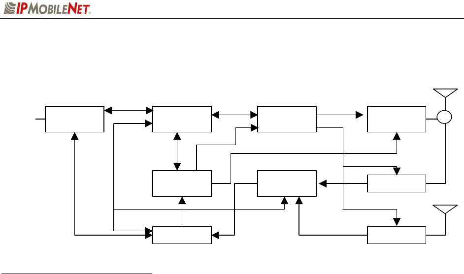
General Block Diagram
General Block Diagram Definitions
The standard IP circuit board contains ten (10) sections defined below.
Input/Output Circuitry associated with the radio’s DB9 data connector providing all the
RS232 data and handshake functions, including the necessary level
changes.
Microcontroller Manages the operation of the radio loading the selected transmit/receive
frequencies into the injection synthesizer, controls the operation of the
modem, and determines which receiver provides a better signal from a
given transmission. Also provides transmit time-out protection in the event
a fault causes the radio to halt in the transmit mode.
Transmit Modulation Circuitry that amplifies the analog audio signal from the modem and uses it
to modulate the voltage controlled oscillator (VCO) and 10 MHz reference
oscillator in the injection synthesizer section. Modulating the VCO and
reference oscillator simultaneously results in a higher quality FM signal.
Modem Converts serial data into an analog audio waveform for transmission and
analog audio from the receiver to serial data. Serial data appears on the
radio’s RS232 port, which connects a Mobile Data Computer (MDC) or a
Voice Interface Unit (VIU).
The modem supports a 115.2 Kbps data transmission rate on the serial
port, SLIP protocol, and up to 19.2 Kbps over-the-air rate. Within a single
chip it provides forward error detection and correction, bit interleaving for
more robust data communications, and third generation collision detection
and correction capabilities.
Injection Synthesizer Provides programmable, ultra stable signals for the radio. One synthesizer
incorporates phase lock loop technology used for both receiving and
transmitting.
Input /
Output
D
DA
AT
T
A
A
Micro-
Controller
Injection
Synthesizer Transmitter
Transmit
Processin
g
Baseband
Routin
g
Receiver 1
Receiver 2 Modem

SECTION 1: THEORY OF OPERATION
~\Technical Documentation\System Manuals\FCC-Reports\IP8HPV\IP8HPV-FCCRpt.doc Page 4
Low Side Injection In the receive mode, the synthesizer provides a local oscillator signal of 45
MHz below the selected receive channel frequency.
Baseband Routing Allows the microcontroller to select one of the two diversity receiver audio
outputs for demodulation by the modem. Switching is done by the
microcontroller comparing the Received Signal Strength Indication (RSSI)
outputs from each receiver. Provision is also made for switching an
external modulation source from the DB9 data connector to the transmitter
input.
Transmitter/TR Switch Consists of an exciter and power amplifier module. The transmitter
circuitry includes a T/R switch switching the antenna between transmitter
and receiver 1 (TX/RX1).
Receiver 1/Receiver 2 Required to support the mobile DRS; two (2) discrete receivers are tuned
to the same channel and use two (2) antennas.
The receivers are double-conversion superheterodyne with a first
Intermediate Frequency (IF) of 45 MHz and a second IF frequency of 455
KHz. Each receiver consists of bandpass filters, an RF amplifier, a crystal
filter, a double-balanced mixer, and a one-chip IF system. The injection
synthesizer provides the first local oscillator signal. Outputs from each
receiver include RSSI and analog audio for the baseband routing circuitry
and modem.
Power Supply Consists of circuitry that derives the various operating voltages for the
radio. A group of fixed and adjustable voltage regulators are used for this
purpose. The transmitter power control circuitry is also found in this
section.

SECTION 1: THEORY OF OPERATION
~\Technical Documentation\System Manuals\FCC-Reports\IP8HPV\IP8HPV-FCCRpt.doc Page 5
IP8 HPV Data Transceiver Section Descriptions
This section provides detailed descriptions of each of the sections within the IP8 HPV Data Transceiver.
Refer to Appendix A to view the IP8 HPV Data Transceiver Circuit Board Diagram (Top and Bottom
views).
Microcontroller
The microcontroller is a major component of the radio as it manages the operation of the radio loading the
selected transmit/receive frequencies into the injection sythesizer. It also controls the operation of the
modem, and determines which receiver provides a better signal from a given transmission. It provides
transmit time-out protection in the event a fault causes the radio to halt in the transmit mode.
It utilizes a reduced instruction set computer (RISC) architecture which provides low power operation and
a powerful instruction set. Other features include:
• Watchdog timer
• Serial UART
• Two 8-bit timers
• 2 KB EEPROM storage
Support circuitry
The support circuitry consists of the following:
A Supervisor Control Chip providing power-on reset.
A clock controlling the microcontroller operation and is generated by crystal Y3 and a Pierce oscillator
circuit inside the microcontroller.
The latch decodes low order address bits from the address/data bits. It enables Address Latch
Enable (ALE) output of the microcontroller and the bits are used by the modem and synthesizer
circuitry.
A 512Kx8 Static RAM Chip provides temporary storage of the radio’s configuration data facilitating
the technician with access to make changes.
Glue logic, also an important part in the microcontroller section. The RAM chip select and modem
chip select command lines are created by gates that decode four (4) high order address bits, plus the
read and write command lines. The RAM is addressed by five (5) memory addresses bits decoded
by logic that decodes port address bits to produce memory address bits for the RAM chip.
Input/Output
Input/output components convert serial and handshake data from the modem section to RS232 levels,
and vice-versa. A transceiver chip is an RS232 transmitter and receiver and converts data in 5-volt logic
form to data in +/-12-volt form, as required by the RS232 standard. A charge pump power supply on the
chip converts the +5-volt DC logic power on pin 26 to the +12-volt and –12-volt levels required.
Capacitors C106-C109 generate these voltages by a charge pump. These values determine the
operating voltages.
This section also includes a DIP switch and an octal tri-state buffer. S1 provides hardware programming
for external modulation. This buffer is used only in MDT-870 applications. When enabled by S1

SECTION 1: THEORY OF OPERATION
~\Technical Documentation\System Manuals\FCC-Reports\IP8HPV\IP8HPV-FCCRpt.doc Page 6
(870MODE line), it provides a serial interface for the MDT-870. Notice that only the RX data (RXD) and
all handshake lines are buffered. Transmit data (TXD) is derived from a modem interface circuit.
Injection Synthesizer
The synthesizer chip is the major contributor of the injection synthesizer. This device contains the key
components of a phase locked loop (PLL), including a prescaler, programmable divider, and phase
detector. The selected frequencies are loaded into the synthesizer chip as a clocked serial bit stream via
the PLL DATA and PLL CLOCK inputs. The microcontroller provides the serial data.
A 10 MHz reference frequency is provided by voltage controlled, temperature controlled crystal oscillator
module. This device has an input that accepts transmit modulation and voltage from a RX FREQ
ADJUST pot. The pot allows the receiver to be fine-tuned to the exact operating frequency.
The injection signals are generated by a voltage controlled oscillator (VCO) module VCO1 (approximately
850-870 MHz). A voltage on the C input determines the VCO frequency. The voltage is generated by the
phase detector output (PDOUT) of U14 driving a loop filter consisting of R42, C50, C51, and R39. It
integrates the pulses that normally appear on PDOUT into a smooth DC control signal for the VCO. Upon
transmit, the analog signal from the modem and transmit modulation circuitry is applied to VCO1 via the
M input.
The output of VCO1 passes through a high-linear switch (SW3), which is then attenuated by resistors
R114-R116 for improved loop stability, and then amplified by an RF amplifier (U11). From U11 the signal
passes through a two-way divider (U10). One port of U10 passes through another two-way divider (U12).
The first port of U12 provides the receive injection (RXINJ1) signal for Receiver 1, while the second port
output provides the receive injection (RXINJ2) signal for Receiver 2. The other port of U10 passes
through another two-way divider (U13). One port returns to the synthesizer FIN+ input via the VCO
feedback completing the loop signal path. The other port of U13 provides the transmit injection (TXINJ)
signal for the transmitter circuit.
A second VCO module (VCO2) is included for future applications.
Transmitter/TR Switch
The transmitter section consists of an exciter, power amplifier, and power control circuitry. The exciter is
built around an RF power amplifier chip. To transmit, TXKEYOUT* is pulled low. This causes this
amplifier to power up and amplify the TXINJ signal input through a voltage variable absorptive attenuator.
PA12V is also powered up. This causes the power amplifier to boost the RF power to the desired level.
Up to 16 watts are available from the transmitter.
Receiver 1 Front-End
This section consists of the components that form Receiver 1 Front-End. These components include
surface acoustic wave (SAW) filters, a low-noise amplifier, and a mixer.
Incoming signals pass through a low-loss SAW filter that provides a high degree of out-of-band signal
rejection. A low-noise amplifier amplifies the selected signals and another low-loss SAW filter provides
additional selectivity. The output from this low-loss SAW filter connects to a mixer. This mixer is a MMIC
mixer which heterodynes the receive injection signal from the synthesizer. The result is a 45 MHz IF
signal and the IF signal goes through crystal filters (FLT3 and FLT4) to the Receiver 1 IF section for
further processing.

SECTION 1: THEORY OF OPERATION
~\Technical Documentation\System Manuals\FCC-Reports\IP8HPV\IP8HPV-FCCRpt.doc Page 7
Receiver 1 IF
This section consists of 1 IF subsystem. The major contributor of the IF subsystem a complete 45 MHz
superheterodyne receiver chip incorporating a mixer/oscillator, two limiting intermediate frequency
amplifiers, quadrature detector, logarithmic received signal strength indicator (RSSI), voltage regulator
and audio and RSSI op amps.
Incoming 45 MHz signals appearing at RX1_45MHz pass through a low-voltage high performance
monolithic FM IF system. Within this system, the signals pass through a simple LC filter and are boosted
by the RF amplifier. The output of the RF amplifier drives a mixer. A crystal oscillator is controlled by
crystal Y4 and provides the injection frequency for the mixer. The mixer output passes through a 455
KHz ceramic filter. It is then amplified and passed through another ceramic filter to a second gain stage.
The IF output drives a quadrature detector. The RSSI1 detector converts the AGC voltage generated
inside the chip into a DC level corresponding logarithmically to the signal strength. The Diversity
Reception Controller uses signal BRSSI1 to select the receiver with the best quality signal.
The audio is amplified by an op amp and delivered to the baseband routing circuitry via the RXMOD1
output. High frequency de-emphasis is provided by a filter consisting of a resistor and a capacitor. In
order to match the audio signal levels with the other circuitry, a gain control is included. A pot is
necessary to adjust gain.
Transmit Modulation
The analog circuitry in this section modulates the Transmitter. The data-bearing audio signal from the
modem appears at TXMOD. The audio is amplified by op amp (U9D). The output of the op amp drives
two (2) amplifiers (U9B and U9C).
The upper amplifier (U9C) has adjustable gain. The output drives op amp (U9A), which inverts the phase
of the signal. Upon the start of a transmission, the modulating signal passes through to the 10 MHz
reference oscillator in the synthesizer. Some makes of 10 MHz oscillators do not require the modulation
signal to be inverted and a jumper block is provided to accommodate the oscillators. The lower op amp
(U9B) amplifies the signal and applies it to the VCO via the VCOMOD output.
Baseband Routing
This circuitry routes the audio signal from a Receiver to the modem circuit. Provisions are also made to
route an analog modulation source attached to the radio to the transmitter.
During the receive operation, data-bearing audio signals from the two (2) receivers pass through an IC
analog switch (SW2). The microcontroller makes the TXKEYOUT* line high and the RX1/RX2* line high
or low to pass data from Receiver 1 or Receiver 2. The Receiver audio signal appearing on pin 5 of the
analog switch is routed directly to the modem circuit via DIVAUDIO. Simultaneously, the data-bearing
audio signal is routed through an eighth order Bessel filter (U6). The filter removes high frequency
signals from the data.
In the transmit mode, when external modulation is selected with the DIP Switch, voice audio arriving on
pin 5 of the RS232 data connector appears at the input of analog switch. The controller makes
TXKEYOUT* low, and RX1/RX2* high in order to pass the audio signal through the analog switch.

SECTION 1: THEORY OF OPERATION
~\Technical Documentation\System Manuals\FCC-Reports\IP8HPV\IP8HPV-FCCRpt.doc Page 8
Power and Analog Ground
These sections consist of the power supplies and transmit control circuitry. Power from the vehicle’s
battery appears at VBATT. A diode protects the voltage regulators by clamping any transient spikes on
the supply line. Such spikes typically occur while the engine is started. The supply line powers a series
of voltage regulators and the transmitter control circuitry, as follows:
Voltage regulator VR1 provides switched 9-volt power for most other sections in the radio.
Voltage regulator U21 powers the analog circuitry in the radio and is also switched on by the
microcontroller.
Voltage regulator VR2 provides a low noise 3.3-volt source for the synthesizer chip.
In the transmit control circuitry, to transmit, the microcontroller makes TXKEYOUT* high forcing the P-
channel device to conduct, applying 12-volts via PA12V to the transmitter power amplifier.
Receiver 2 Front-End
The circuitry for Receiver 2 is identical to Receiver 1.
Receiver 2 IF
This section is identical to the Receiver 1 IF.
Modem
The IP uses a single-chip modem circuit that converts serial data to an analog audio waveform for
transmission and analog audio from a receiver to serial data. In addition to the modem functions, the chip
provides forward error detection and correction, bit interleaving for more robust data communications, and
third generation collision detection and correction capabilities.
The microcontroller section controls the modem operation. Address bus, address/data bus, and control
lines operate the modem chip. The modem circuitry is also run by a crystal-controlled clock, which
consists of crystal Y1 and an internal Pierce oscillator.
Incoming audio from the baseband routing circuit appears on the DIVAUDIO input. The audio signal is
demodulated into digital data appearing on the AD0-AD7 lines when the MODEMCS* and RD* lines are
low. The data goes to the microcontroller section for further processing, and then to the input/output
section for conversion to RS232 signal levels. At this point, the received data is available to the user’s
MDC and VIU.
During a transmission, outgoing data appearing on the AD0-AD7 lines is converted into a 4-level FSK
audio signal by the modem chip. This operation takes place when the MODEMCS* and WR* lines are
low. Data from the user’s MDC or VIU passes through the input/output section and microcontroller
section to the AD0-AD7 bus. After processing, data passes through a root raised cosine filter and is
output to TXMOD.
This modem supports 115.2 KBPS (serial port) and 19.2 KBPS (over-the-air) data transmission rates.

SECTION 1: THEORY OF OPERATION
~\Technical Documentation\System Manuals\FCC-Reports\IP8HPV\IP8HPV-FCCRpt.doc Page 9
VLogic and Digital Ground
The VLogic and Digital Ground section consists of a pulse-width modulation (PWM) step-down DC-DC
converter (U20) that provides an adjustable output. It also reduces noise in sensitive communications
applications and minimizes drop out voltage.
An external Schottky diode (D2) is required as an output rectifier to pass inductor current during the
second half of each cycle to prevent the slow internal diode of the N-channel MOSFET from turning on.
This diode operates in pulse-frequency modulation (PFM) mode and during transition periods while the
synchronous rectifier is off.
SECTION 2: FACTORY TEST PROCEDURE
~\Technical Documentation\System Manuals\FCC-Reports\IP8HPV\IP8HPV-FCCRpt.doc Page 10
Equipment List
The following table lists the equipment required to perform the IP8 HPV Mobile Radio Factory Test
Procedure:
QTY DESCRIPTION MANUFACTURE MODEL
1 Communications Test Set HP Hp 8920A or B
1 Hi Freq Probe HP HP8502A
1 Power Supply for HP8502A Probe HP HP1122A
1 4 Channel Scope Tektronix TDS 460A
2 General Propose Scope Probe
1 DVM Tektronix
Fluke
DMM912
77
1 Attenuator 40 dB 100W
1 IP8 HPV Base Station
1 IP Network Controller
2 12V Power Supply
2
PC’s
One for the Mobile
One Base
Windows 9X w/
IPMessage
AVR

SECTION 2: FACTORY TEST PROCEDURE
~\Technical Documentation\System Manuals\FCC-Reports\IP8HPV\IP8HPV-FCCRpt.doc Page 11
Programming and Configuring Mobile Radio
Once the appropriate equipment for performing the factory test are gathered, perform the following steps
to program and configure an IP8 HPV Mobile Radio:
Step 1 Enter the following information on the Mobile Radio Performance Test Data Sheet:
Radio Serial number
Date test being performed
Tester's Name
Step 2 Program the radio to the current Firmware revision using the AVR programming utility.
Step 3 Connect a PC to the radio using IPMessage program. In the IPMessage window, type in the
following command:
factory default
Press the [ENTER] key and the radio will load default configuration values into the
IPMessage window.
Step 4 Enter the appropriate values for the radio's frequency band.
Example: The following values were used for a 806 to 869 MHz radio:
[To: Radio] ?
[From: 192.168.3.10] Host serial = 19200,N,8,1, timeout=200
[From: 192.168.3.10] Host framing =
[From: 192.168.3.10] SLIP no status messages
[From: 192.168.3.10] Injection = LOW SIDE, 45MHz
[From: 192.168.3.10] channel spacing = 25000
[From: 192.168.3.10] Channel = 0
[From: 192.168.3.10] TX Power = 0
[From: 192.168.3.10] Car to car TX power = 0
[From: 192.168.3.10] Channel Tx freq Rx freq Inj freq
[From: 192.168.3.10] Frequency= 0, 815.10000, 860.10000, 815.100000
[From: 192.168.3.10] Serial number: undefined
[From: 192.168.3.10] TX quiet time = 5
[From: 192.168.3.10] TX sync time = 12 milliseconds, 0 extra inter-split-frame count
[From: 192.168.3.10] TX tail time = 5
[From: 192.168.3.10] Radio data rate = 19200
[From: 192.168.3.10] Max data tx time = 60 seconds
[From: 192.168.3.10] PLL load to txkey delay = 2 milliseconds
[From: 192.168.3.10] Carrier detect delay time = 3 milliseconds
[From: 192.168.3.10] Polarity = TX-, RX+
[From: 192.168.3.10] allow crc errors = 0
[From: 192.168.3.10] Duplicate time = 10 milliseconds
[From: 192.168.3.10] RSSI step = 12 (=234mV)
[From: 192.168.3.10] noise = -62dBm, -131dBm
[From: 192.168.3.10] Fixed TX Delay = 0 milliseconds
[From: 192.168.3.10] Scale TX Delay = 0 microseconds
[From: 192.168.3.10] IP Address = 192.168.3.10 (VIU = 172.16.19.1, PC = 172.16.18.1)
[From: 192.168.3.10] netmask = 255.255.255.0
[From: 192.168.3.10] num timeslots = 16
[From: 192.168.3.10] timeslot period = 992ms
[From: 192.168.3.10] timeslots per voice packet = 4
[From: 192.168.3.10] 15Sep2000 04:54:46 (PST), calibration=511
[From: 192.168.3.10] diversity speed = 5
[From: 192.168.3.10] receiver = auto

SECTION 2: FACTORY TEST PROCEDURE
~\Technical Documentation\System Manuals\FCC-Reports\IP8HPV\IP8HPV-FCCRpt.doc Page 12
Adjustment / Alignment Procedures
Receiver Injection
Perform the following steps to adjust the receiver injection and injection frequency:
Step 1 While monitoring the receiver injection frequency at C64, adjust potentiometer RV3 for
minimum frequency error of +/- 100Hz. Record this value on the Mobile Radio Performance
Test Data Sheet.
Step 2 RX1 - While monitoring the 44.545 MHz 2nd injection frequency at U33 pin 4, adjust trimmer
capacitor CV1 for the maximum amplitude of this injection frequency. The maximum
amplitude must be between +3 to +5 dBm. Record this value on the Mobile Radio
Performance Test Data Sheet.
Step 3 RX2 – While monitoring the 44.545 MHz 2nd injection frequency at U34 pin 4, adjust trimmer
capacitor C159 for the maximum amplitude of this injection frequency. The maximum
amplitude must be between +3 to +5 dBm. Record this value on the Mobile Radio
Performance Test Data Sheet.
Receiver 1
Perform the following steps to adjust receiver 1:
Step1 Inject an on-frequency carrier signal with an amplitude of -80 dBm, modulated with a 1 kHz
test tone at +/- 5.0 kHz deviation into receiver 1's antenna port.
Step 2 The RSSI value should be between 1.3 and 1.5 VDC for a properly tuned radio. Record this
value on the Mobile Radio Performance Test Data Sheet.
Step 3 While monitoring the DC level of the recovered modulation at TP1, adjust potentiometer R82
for 2.500 VDC +/- 1 mV DC.
Step 4 While monitoring the amplitude of the recovered audio signal at TP1, adjust potentiometer
R81 for 350 mV RMS +/- 1 mV RMS.
Step 5 While monitoring the recovered audio signal at TP1, verify the distortion is less than 3%.
Record this value on the Mobile Radio Performance Test Data Sheet.
Step 6 While monitoring the recovered audio signal at TP1, verify the SINAD is -119 dBm or better.
Record this value on the Mobile Radio Performance Test Data Sheet.
Step 7 R81 and R82 are interactive adjustments; therefore, continue adjusting R81 and R82 until the
Audio AC & DC Amplitudes are within the respective limits. Record these values on the
Mobile Radio Performance Test Data Sheet.

SECTION 2: FACTORY TEST PROCEDURE
~\Technical Documentation\System Manuals\FCC-Reports\IP8HPV\IP8HPV-FCCRpt.doc Page 13
Receiver 2
Perform the following steps to adjust receiver 2:
Step 1 Inject an on-frequency carrier signal with an amplitude of -80 dBm, modulated with a 1 kHz
test tone at +/- 5.0 kHz deviation into Receiver 2's antenna port.
Step 2 The RSSI value should be between 1.3 and 1.5 VDC for a properly tuned radio. Record this
value on the Mobile Radio Performance Test Data Sheet.
Step 3 While monitoring the DC level of the recovered modulation, adjust potentiometer R93 for
2.500 VDC +/- 1 mV DC
Step 4 While monitoring the amplitude of the recovered audio signal, adjust potentiometer R99 for
350 mV RMS +/- 1 mV RMS.
Step 5 While monitoring the recovered audio signal at TP1, verify the distortion is less than 3%.
Record this value on the Mobile Radio Performance Test Data Sheet.
Step 6 While monitoring the recovered audio signal at TP1, verify the SINAD is -119 dBm or better.
Record this value on the Mobile Radio Performance Test Data Sheet.
Step 7 R93 and R99 are interactive adjustments; therefore, continue adjusting R93 for 350 mVRMS
and R99 for 2.500 VDC until further adjustments are no longer necessary. Record these
values on the Mobile Radio Performance Test Data Sheet.
Transmit Data
Perform the following steps to adjust transmit data:
Step 1 Use IPMessage to set the transmit power to 0.
Step 2 Using the x=2000,n command of IPMessage to generate transmit data messages while
observing the transmitted signal on the HP RF communications test set, adjust R33 for
minimum frequency error while transmitting data messages.
Step 3 Turn potentiometer RV2 fully counterclockwise.
Step 4 Adjust RV1 for a maximum deviation of 5 KHz.
Step 5 Using calibrated base station, and monitoring the uplink received data quality on the base
station's Hyperterminal screen, slowly turn RV2 clockwise until consistent data quality
readings of 240 - 248 are achieved using 2000 character test messages. Data quality
reading should not be less than 240 for 2000 character messages.
If unable to reach the data quality readings then ask for Technical Support. Poor data
quality readings are indicative of poor group delay performance.
Step 6 Verify transmit deviation, frequency error, and transmitting data messages quality and record
this data on the Mobile Radio Performance Test Data Sheet.

SECTION 2: FACTORY TEST PROCEDURE
~\Technical Documentation\System Manuals\FCC-Reports\IP8HPV\IP8HPV-FCCRpt.doc Page 14
Transmit Power Control
Perform the following steps to adjust the transmit power control:
Step 1 Using the x=2000,n command of IPMessage, and while monitoring the transmit power level
on the HP communications test set, check the level of the transmit power. Using IPMessage
set the power setting to txpower=0. The radio should have an output power level of
approximately 1 mW. Record this value on the Mobile Radio Performance Test Data
Sheet.
Step 2 Using IPMessage send the txpower= command to increase the power level settings until 16
Watts of output power is obtained. Record this value on the Mobile Radio Performance
Test Data Sheet. Note that values on the table are to plot the codes vs. power output. The
16-Watt setting can be a code not on the table. Adjust txpower until the code is found that
does not exceed 16.0 Watts. Record this value on the Mobile Radio Performance Test
Data Sheet.
Do not to exceed 16 Watts of output power, as this will reduce the life of the amplifier.
Receive Data
Perform the following steps to adjust the receive data:
Step 1 Attach a power attenuator to the TX port on the radio.
Step 2 Using the DOS ping command on the PC connected to the radio, ping the network controller
to generate uplink and downlink data messages. The following command will generate one
Hundred 500 character messages:
>;Ping 192.168.3.3 -n 100 -l 500
Step 3 Observe the data quality readings on the IPMessage window of the PC connected to the
radio using the V (for Verbose) command in the IPMessage program. With the mobile radio's
antenna connected to receiver 1, verify the received data quality readings are consistently
248s. Data quality readings should also be verified at the base station using the V command
on the Hyperterminal window.
Step 3 Verify receiver 2 data quality readings are also consistently 240 to 248s by changing the
antenna from receiver 1 port to receiver 2 port. In this manner both uplink and downlink data
quality can be verified. Record this data on the Mobile Radio Performance Test Data
Sheet.

SECTION 2: FACTORY TEST PROCEDURE
~\Technical Documentation\System Manuals\FCC-Reports\IP8HPV\IP8HPV-FCCRpt.doc Page 15
Final Test
A final test must be performed prior to shipping the IP8 HPV mobile radio to the customer. This final test
will verify that the timing characteristics are correct and that both transmit and receive data quality
readings are consistently high.
Perform the following steps for the final test:
Step 1 Attach the 40dB 100-Watt power attenuator to the transmit port of the radio.
Step 2 Program the radio for full power operation. The tx power level setting can be found in the
radio's Mobile Radio Performance Test Data Sheet.
The setting must not to exceed 16 Watts.
Step 3 Attach a digital scope to the base station as described in section the next section, Uplink
Hardware Timing Verification. Using the x=2000,19 command (which will cause the radio
to transmit 19 2000 character messages), verify the following:
Transmit frequency of radio is adjusted for minimum frequency error of +/- 500 Hz.
The x=2000,19 command will generate different messages with differing DC components.
Each message will slightly slew the frequency off from the center frequency). Be careful to
closely monitor the variation in transmit frequency due to these different messages and
ensure that on average the transit frequency error has been minimized to within +/-500 Hz.
This indicates that some of these test messages will be slightly high in frequency, some
messages will be slightly low in frequency, and some messages will be right on frequency.
Step 4 Verify the transmit a maximum deviation of 5 KHz.
Step 5 Verify the timing characteristics are identical to the plots in the next section, Uplink
Hardware Timing Verification.
Step 6 At the base station monitor PC, verify that all the data quality readings are 240 and higher.
Step 7 Move the scope probes to monitor the timing at the mobile radio as described in Downlink
Hardware Timing Verification. Generate test messages by pinging the IPNC from the PC
attached to the radio. The following command will cause 100 pings, 500 bytes in length to be
transmitted from the mobile radio and echoed by the IPNC through the base station:
.>;Ping 192.168.3.3 -n 100 -l 500 -w 2000
Step 8 Set CRC =1 Enable on the radio
Step 9 Verify the timing characteristics are identical to those in Downlink Hardware Timing
Verification.
Step 10 Verify that both receivers on the mobile radio report data quality readings of 240 or higher
(248 is typical). This can be accomplished by installing the antenna on the TX/RX1 port and
verifying RX1 is selected by observing the RX1 LED on the mobile radio and installing the

SECTION 2: FACTORY TEST PROCEDURE
~\Technical Documentation\System Manuals\FCC-Reports\IP8HPV\IP8HPV-FCCRpt.doc Page 16
antenna on the RX2 port and verifying RX2 is selected by observing the RX2 LED on the
mobile radio.
Step 11 Reset CRC =0 Disable on the radio
Step 12 In IPMessage, type the ? command to radio. Copy the radio settings and paste them into the
IP8HPV Mobile Radio Performance Test Data File.
Step 13 Perform a close visual inspection of the radio closely inspecting manufacturing related
problems (loose screws, solder particles, etc.).
SECTION 2: FACTORY TEST PROCEDURE
~\Technical Documentation\System Manuals\FCC-Reports\IP8HPV\IP8HPV-FCCRpt.doc Page 17
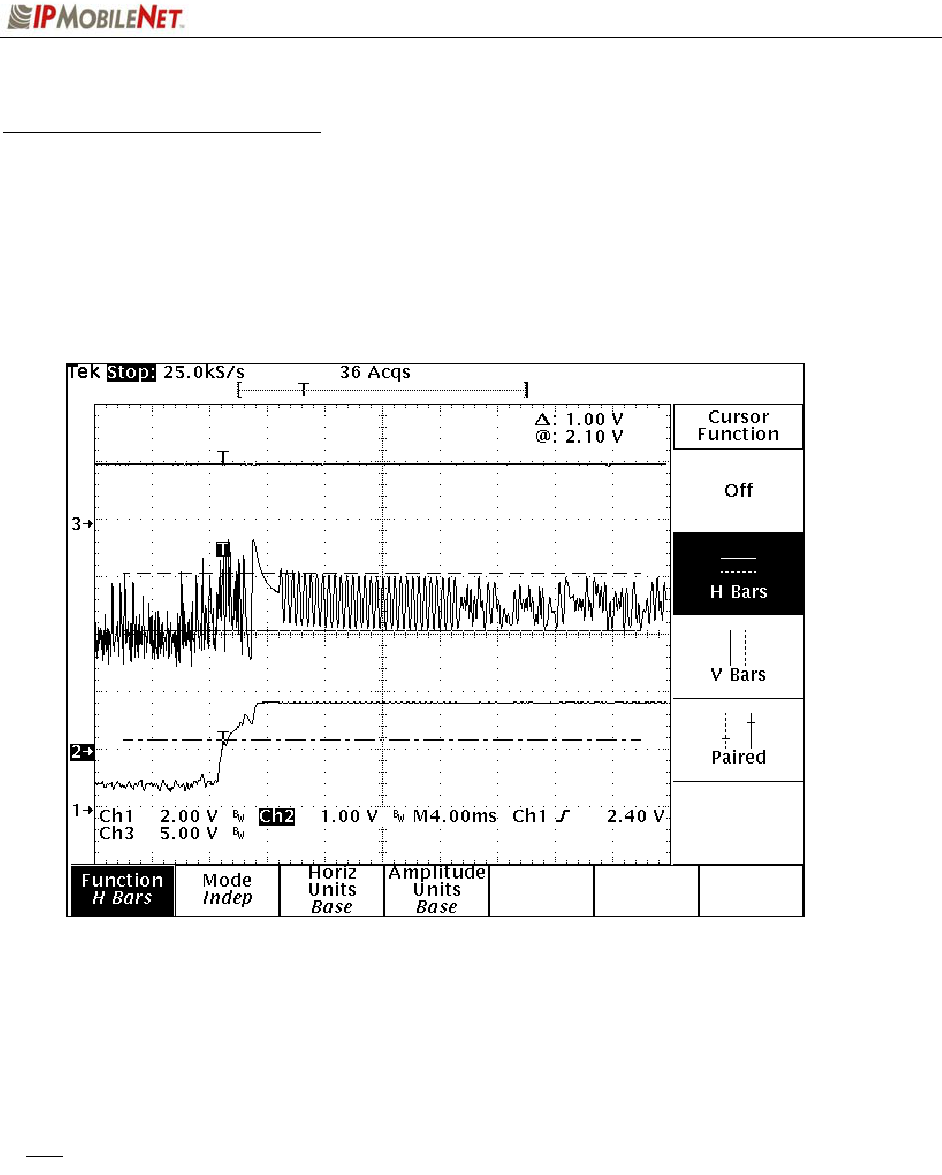
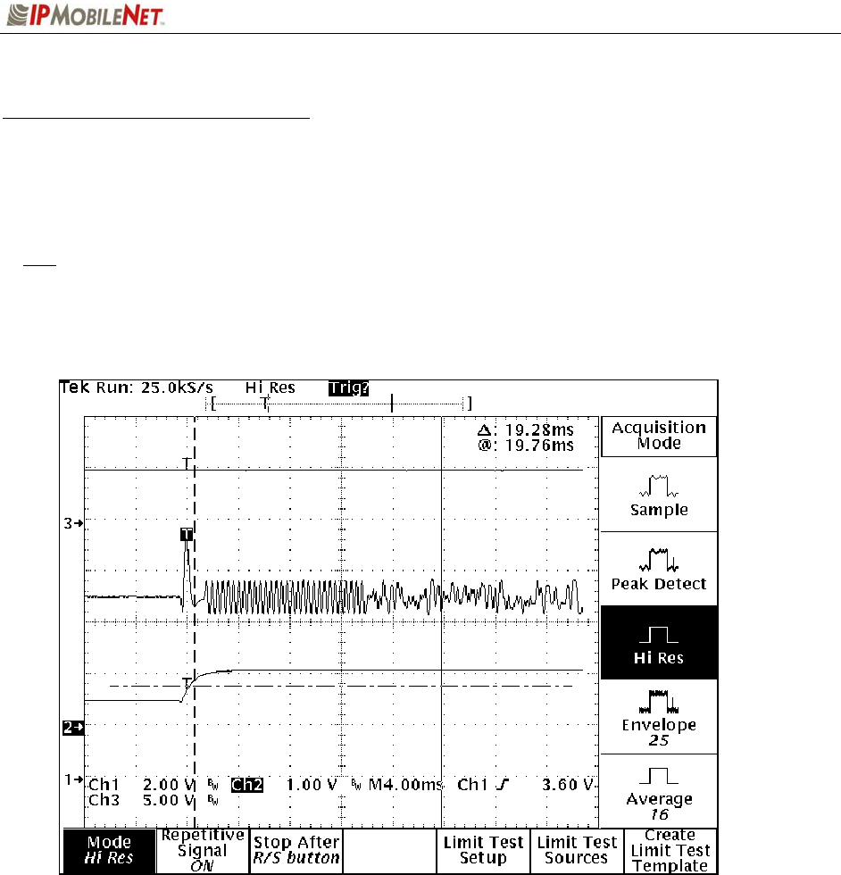
Uplink Hardware Timing Verification
Figure 2-1 below displays an oscilloscope plot of an uplink data message from the mobile to the base
station. Channel 1 is connected to the base station's RSSI (XXX-12), channel 2 is connected to the base
station's recovered modulation (TP6), and channel 3 is connected to the base station's modem chip select
line. The scopes acquisition mode is high-resolution.
Figure 2-1: Oscilloscope Plot of an Uplink Data Message
As seen in the above plot, the mobile radio's transmit carrier has ramped up to full power (channel 1) in
just a few milliseconds. The recovered modulation (channel 2) is stable by this time. There follows a few
milliseconds of quiet time followed by 12 milliseconds of symbol sync time.
The recovered modulation from a mobile radio should look identical to this plot. The recovered
modulation signal should be approximately 1.0 Volts peak-to-peak and should be centered at
approximately 2.5 VDC as is indicated in the figure above.
SECTION 2: FACTORY TEST PROCEDURE
~\Technical Documentation\System Manuals\FCC-Reports\IP8HPV\IP8HPV-FCCRpt.doc Page 18
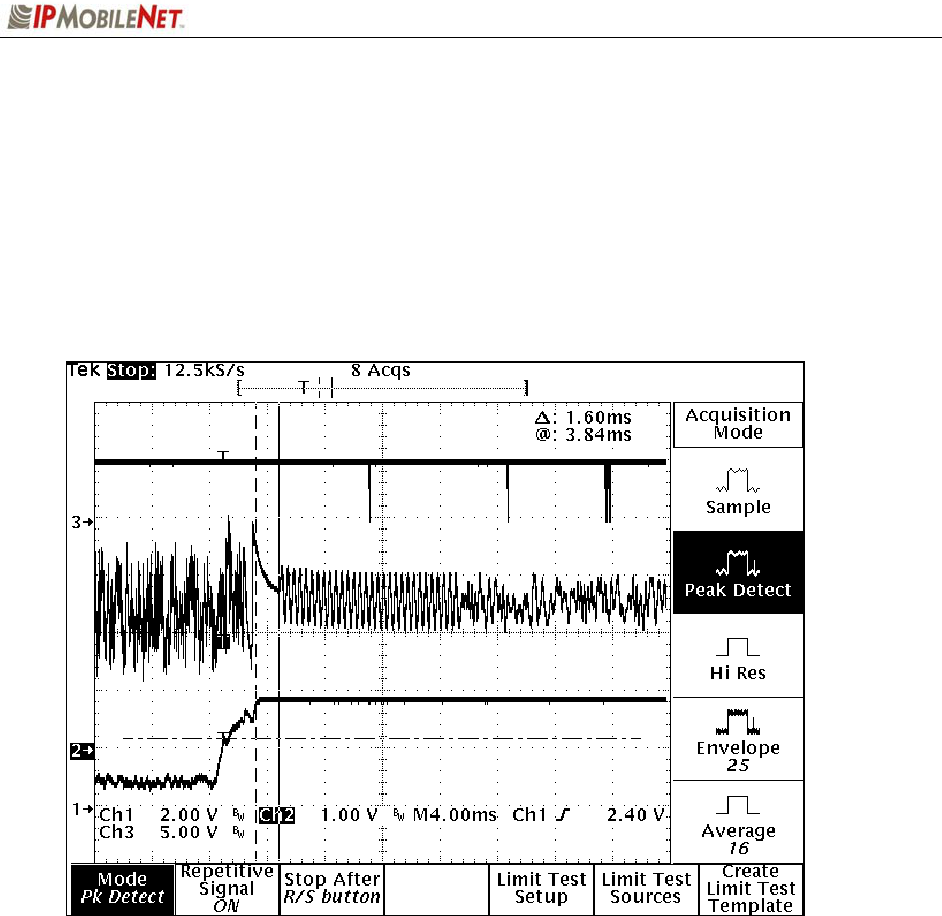
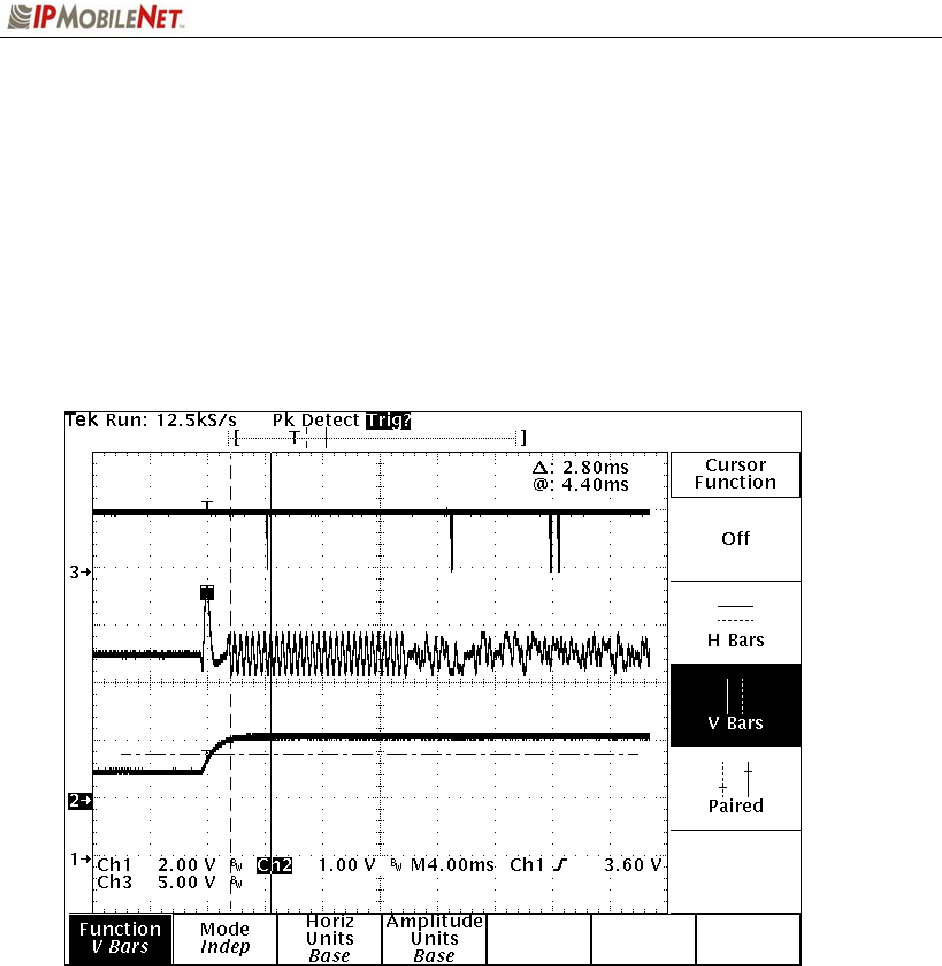
Figure 2-2 displays another oscilloscope plot of an up-link data message from the mobile to the base
station. As in the last plot, channel 1 is connected to the base station's RSSI (J5-12), channel 2 is
connected to the base station's recovered modulation test point (TP6), and channel 3 is connected to the
base station's modem chip select line (U16-13). The scope's acquisition mode is now in the peak detect
mode. This enables the base station's modem CS (Chip Select) line to be viewed.
Figure 2-2: Another Oscilloscope Plot of an Uplink Data Message
The base station's microcontroller, upon detecting a step response in the RSSI (caused by the mobile
radio's transmitter coming up to power), waits a period of time equal to the programmed value of the base
station's carrier detect delay time. The microcontroller then instructs the modem to search for the modem
synchronization preamble. When the base station instructs the modem to look for sync tones, the
modem's CS line transitions low. This can be seen in the above plot. Approximately 10 milliseconds after
the mobile radio's transmitter causes a step increase in the base station's RSSI, the CS signal goes low
momentarily. As can be seen, the sync tones are stable by this time and the modem quickly establishes
synchronization.
SECTION 2: FACTORY TEST PROCEDURE
~\Technical Documentation\System Manuals\FCC-Reports\IP8HPV\IP8HPV-FCCRpt.doc Page 19
Downlink Hardware Timing Verification
Figure 2-3 displays a plot of the downlink timing characteristics. Channel 1 is connected to RSSI,
channel 2 is connected to recovered audio, and channel 3 is connected to the modem CS pin. The scope
is in the high-resolution acquisition mode.
There is a very short period of quiet time (no modulation) followed by approximately 12 milliseconds of
modem synchronization time (sync time).
Figure 2-3: Downlink Timing Characteristics Plot
SECTION 2: FACTORY TEST PROCEDURE
~\Technical Documentation\System Manuals\FCC-Reports\IP8HPV\IP8HPV-FCCRpt.doc Page 20
The plot in Figure 2-4 is the same as before but now the scope is in the peak detect acquisition mode.
After the mobile radio detects a step response in the RSSI (caused by a down-link transmission), the
radio's microcontroller waits an amount of time equal to the programmed value of the "carrier detect delay
time" then instructs the modem to look for frame sync. When the microcontroller instructs the modem to
look for frame sync, it asserts the modem's CS line (active low). In this plot, the modem's CS line can be
seen to transition low approximately 3 milliseconds after the base station's transmitter has come up to full
power.
Figure 2-4: Downlink Timing Characteristics Plot in Peak Detect Acquisition Mode
The recovered modulation should be centered at approximately 2.5 VDC and should have an amplitude
of approximately 800 mV peal-to-peak as indicated in the plot above.
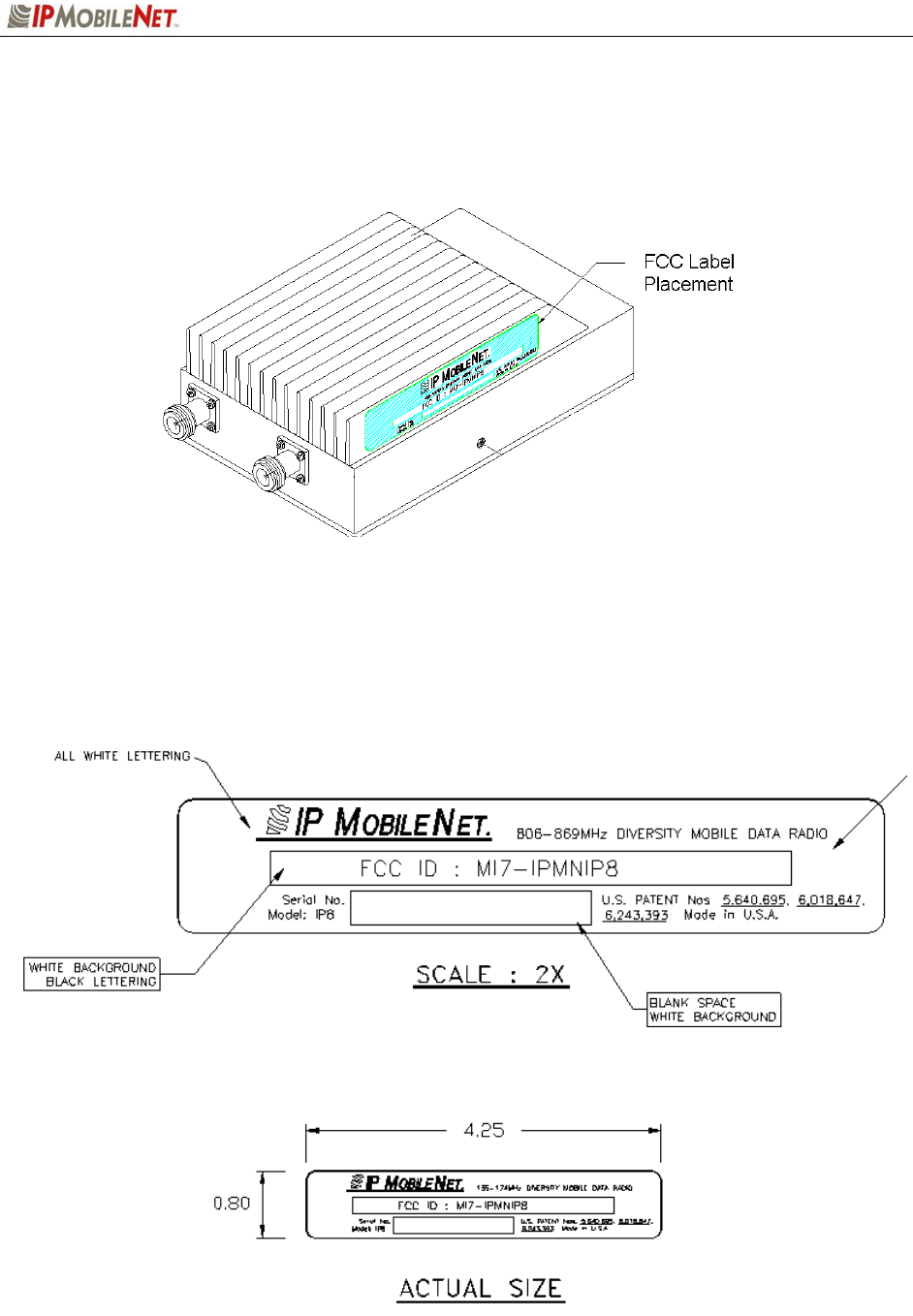
SECTION 3: LABEL AND LABEL PLACEMENT
~\Technical Documentation\System Manuals\FCC-Reports\IP8HPV\IP8HPV-FCCRpt.doc Page 21
INVADR IP8 HPV Data Transceiver FCC Label Placement
INVADR IP8 HPV Data Transceiver FCC Label
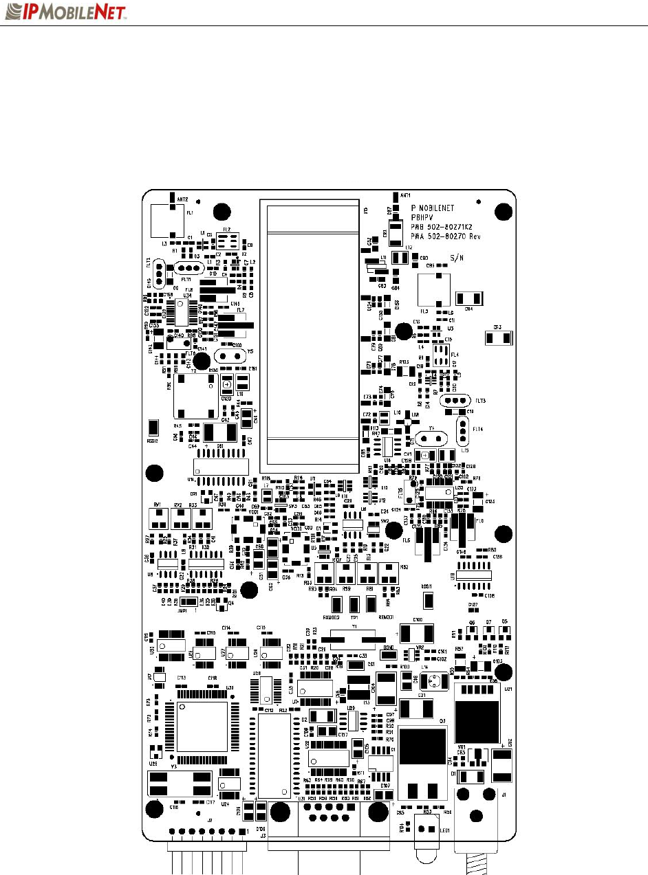
APPENDIX A: CIRCUIT BOARD DIAGRAM
~\Technical Documentation\System Manuals\FCC-Reports\IP8HPV\IP8HPV-FCCRpt.doc Page 22
IP8 HPV Data Transceiver Circuit Board – TOP VIEW
APPENDIX A: CIRCUIT BOARD DIAGRAM
~\Technical Documentation\System Manuals\FCC-Reports\IP8HPV\IP8HPV-FCCRpt.doc Page 23
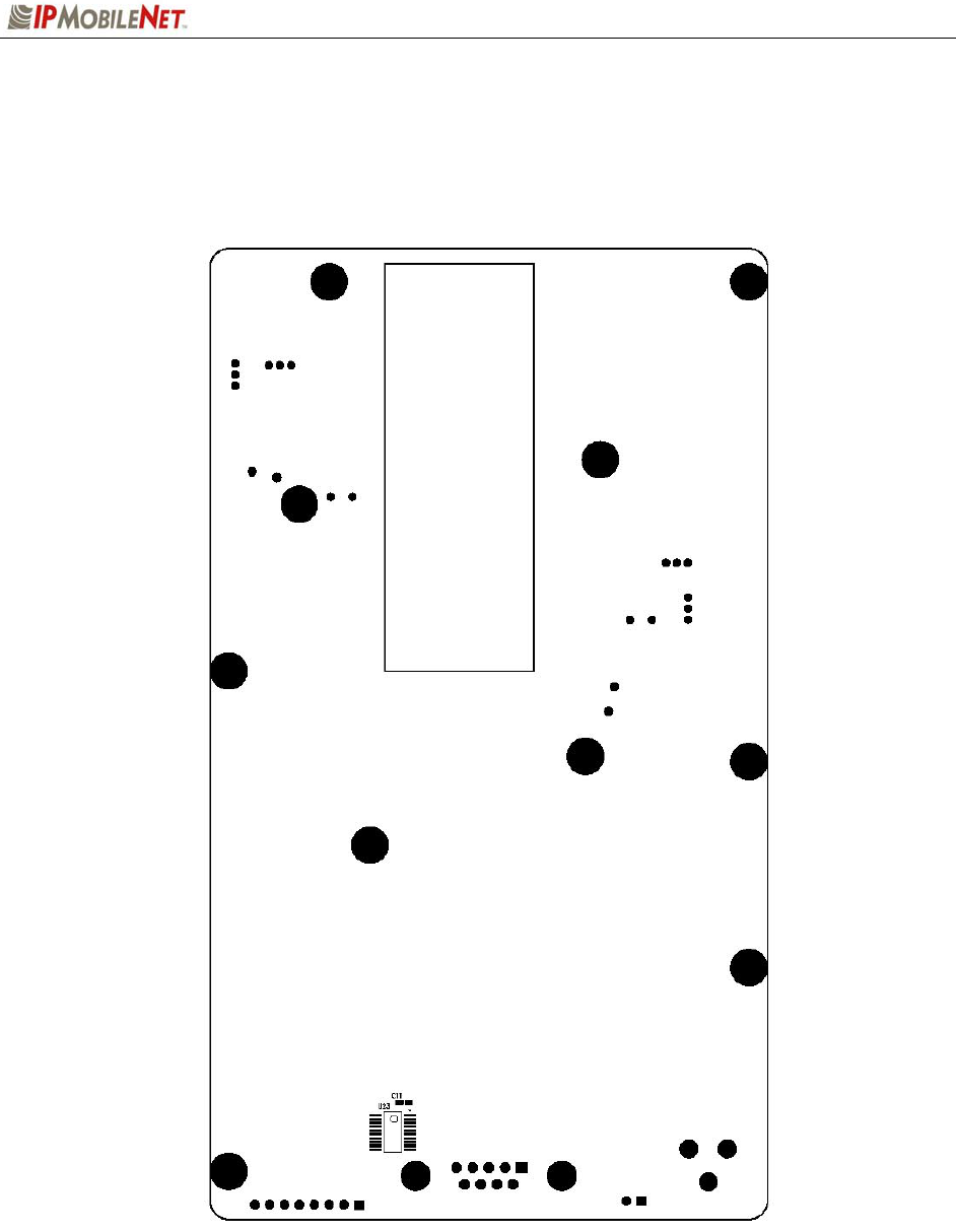
IP8 HPV Data Transceiver Circuit Board – BOTTOM VIEW

APPENDIX B: IP8 HPV TEST DATA SHEET
~\Technical Documentation\System Manuals\FCC-Reports\IP8HPV\IP8HPV-FCCRpt.doc Page 24
Program and Configure Radio
Date
Serial Number
Firmware Revision
Tester
Adjustment / Alignment Procedures
Receiver Injection
Parameter Spec Measured
Injection Frequency Error at
RXINJ1(within +/- 100 Hz of exact
injection frequency)
+/- 100 Hz
U8B pin 4 power level +3 to +5 dBm
Receiver 1& 2
Parameter Spec Reciever 1
Measured Receiver 2
Measured
RSSI test point CV1A adjustment 1.3 to 1.5 VDC
Audio DC Amplitude
(1 kHz Test tone @ 5.0 kHz
Deviation)
2.5 VDC
+/- 1mV
Audio AC Amplitude
(1 kHz Test tone @ 5.0 kHz
Deviation)
350 mVRMS
+/- 1mV
Distortion
(1 kHz Test tone @ 5.0 kHz
Deviation)
3%<
SINAD 12 dB
(1 kHz Test tone @ 5.0 kHz
Deviation)
-119dbm >
APPENDIX B: IP8 HPV TEST DATA SHEET
~\Technical Documentation\System Manuals\FCC-Reports\IP8HPV\IP8HPV-FCCRpt.doc Page 25
Transmit Section
Parameter Spec Measured
Transmit Modulation Deviation
(5.3 kHz while transmitting 2000
character test message)
5.0 KHz Maximum
Transmit Data Quality
(While transmitting 2000 character
test messages to the base station)
240 >
Transmit Frequency Error
(Transmitting 2000 character test
message)
+/- 500Hz
Transmit Power Control (Warning
do not to exceed 16 Watts RF output
power during this pt'> not to exceed 16
Watts RF output power during this test)
Transmit Power Setting Expected
RF Out
RF Out
Watts
0 ~ 1mW
25
50
75
100
125
150
175
200
225
250
Digital Code Measured
Maximum power output setting
without exceeding 16.0 Watts

APPENDIX B: IP8 HPV TEST DATA SHEET
~\Technical Documentation\System Manuals\FCC-Reports\IP8HPV\IP8HPV-FCCRpt.doc Page 26
Data Quality
Parameter Spec Measured
Receiver 1 Data Quality
(While receiving 500 character "pings" from
base station, 100 pings min, no errors
allowed, CRC errors enabled) 240>
Receiver 2 Data Quality
(While receiving 500 character "pings" from
base station, 100 pings min, no errors
allowed, CRC errors enabled) 240>
Final Tests
Uplink Final
Parameter Spec Measured
Transmit Frequency Error
+/- 500 Hz
(Transmitting 19,
2000 character test
message)
Transmit Modulation Deviation 5.0 KHz Maximum
(while transmitting
19,2000 character
test message)
Uplink Hardware Timing Verified
Transmit Carrier ramp up time 2mS < X < 4mS
Symbol Sync time
( Stable Amplitude to with in
100mV during the period) 12ms +/- 1ms
Recovered modulation signal 1 V PtoP ~
2.5 VDC ~

APPENDIX B: IP8 HPV TEST DATA SHEET
~\Technical Documentation\System Manuals\FCC-Reports\IP8HPV\IP8HPV-FCCRpt.doc Page 27
Downlink Final
Parameter Spec Measured
Downlink Hardware Timing
Verification
Recovered Modulation Levels
800 mV~
2.5VDC~
Receiver 1 Data Quality
(While receiving 500 character "pings" from
base station, 100 pings min, no errors
allowed, CRC errors enabled) 240>
LED Receiver 1 Lit
Receiver 2 Data Quality
(While receiving 500 character "pings" from
base station, 100 pings min, no errors
allowed, CRC errors enabled) 240>
LED Receiver 2 Lit
Attach copy of all firmware settings Completed
Visual inspection Completed
Copy Radio Setting into the Cell Below