IP Mobilenet M1617-12 Mobile Station Data Radio Transceiver User Manual 386222
IP Mobilenet, LLC Mobile Station Data Radio Transceiver 386222
UserManual.wiki
>
IP Mobilenet
>
M1617-12 User Manual
>
Users Manual
Contents
1.
Users Manual
2.
Installation Manual
3.
RF Exposure Training
Users Manual
Navigation menu
Upload a User Manual
Namespaces
Wiki Guide
HTML
PDF
Info
Views
User Manual
Discussion / Help
Navigation
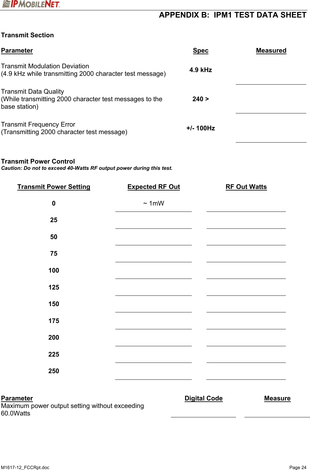
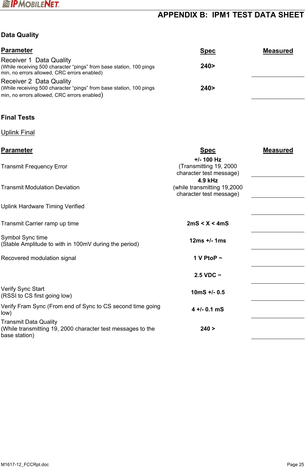
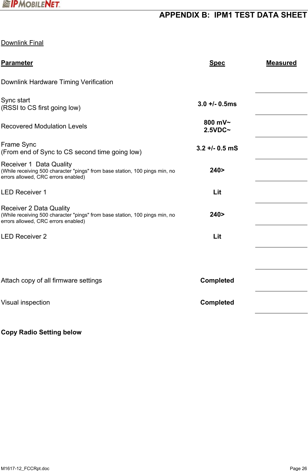
![SECTION 1: THEORY OF OPERATION M1617-12_FCCRpt.doc Page 11 Programming and Configuring Mobile Radio Once the appropriate equipment for performing the factory test are gathered, perform the following steps to program and configure an M1617-12 Mobile Radio: Step 1 Enter the following information on the Test Data Sheet (see Appendix B): Radio Serial number Date test being performed Tester's Name Step 2 Program the radio to the current Firmware revision using the AVR programming utility. Step 3 Connect a PC to the radio and launch the IPMessage program. In the IPMessage window, type factory default, press [ENTER], and the radio displays the radio’s default values. Step 4 Enter the appropriate values for the radio's frequency band. [From: 172.16.64.1] Host serial = 115200,N,8,1, timeout=200 [From: 172.16.64.1] Channel = 0 [From: 172.16.64.1] Channel Tx freq Rx freq Inj freq [From: 172.16.64.1] Frequency= 0, 1##.000000, 1##.000000, 1##.000000 [From: 172.16.64.1] IP Address = 172.16.64.1 (VIU = 0.0.0.0, PC = 192.168.3.5) [From: 172.16.64.1] IPNC = 172.16.112.200 [From: 172.16.64.1] netmask = 255.255.255.0 [From: 172.16.64.1] Radio Mac Address = 00:08:ce:00:00:00 [From: 172.16.64.1] Hosting framing = SLIP no status messages [From: 172.16.64.1] channel spacing = 12.5000 [From: 172.16.64.1] Injection = LOW SIDE, 45 MHz [From: 172.16.64.1] TX Power = 0 [From: 172.16.64.1] Car to car TX power = 0 [From: 172.16.64.1] serial number: undefined [From: 172.16.64.1] TX quiet time = 5 [From: 172.16.64.1] TX sync time = 2- milliseconds [From: 172.16.64.1] TX tail time = 5 [From: 172.16.64.1] TX delay = 0 slots [From: 172.16.64.1] Radio data rate = 19200 [From: 172.16.64.1] Max data tx time = 60 seconds [From: 172.16.64.1] PLL load to txkey delay = 2 milliseconds [From: 172.16.64.1] Carrier detect delay time = 6 milliseconds [From: 172.16.64.1] roam status times = 900 seconds [From: 172.16.64.1] roam lost time = 60 seconds [From: 172.16.64.1] Polarity = TX-, RX+ [From: 172.16.64.1] RSSI step = 12 (=234mV) [From: 172.16.64.1] noise = -126dBm, -126dBm [From: 172.16.64.1] num timeslots = 16 [From: 172.16.64.1] timeslot period = 992ms [From: 172.16.64.1] timeslots per voice packet = 4 [From: 172.16.64.1] 06Feb2036 22:28:34 (PST), calibration=43 [From: 172.16.64.1] diversity speed = 5 [From: 172.16.64.1] receiver = 2 [From: 172.16.64.1] Receiver Hysteresis = 2 [From: 172.16.64.1] Internal GPS Port Address = 5000 [From: 172.16.64.1] Internal GPS Input Protocol = TSIP [From: 172.16.64.1] Internal GPS Output Protocol = TSIP [From: 172.16.64.1] 12dB SINAD = -120dBm (54 on RX0) [From: 172.16.64.1] 12dB SINAD = -120dBm (54 on RX1) [From: 172.16.64.1] 30dB S/N = -106dBm (72 on RX0) [From: 172.16.64.1] 30dB S/N = -106dBm (72 on RX1) [From: 172.16.64.1] 40dB S/N = -90dBm (114 on RX0) [From: 172.16.64.1] 40dB S/N = -90dBm (114 on RX1) [From: 172.16.64.1] –40dBm = (214) on RX0) [From: 172.16.64.1] –40dBm = (214) on RX1) [From: 172.16.64.1] PLL counter: 510.000000 MHz, N = 22200, R = 800 (400x2) [From: 172.16.64.1] Suspend Tx = 0 seconds [From: 172.16.64.1] DHCP Client disabled [From: 172.16.64.1] DHCP Server disabled [From: 172.16.64.1] diag message level = 0 [From: 172.16.64.1] TFTP options = 512 (block size), 0 (interval) [From: 172.16.64.1] Internal GPS not found [From: 172.16.64.1] Modem FEC = on](https://usermanual.wiki/IP-Mobilenet/M1617-12.Users-Manual/User-Guide-386222-Page-11.png)