Ibm Elan Em78P259N 260N Users Manual EM78P259N_260N Product Spec V1.2
EM78P259N260N to the manual d30a6540-4396-43bd-906e-5dbbe4a9f570
2015-02-02
: Ibm Ibm-Elan-Em78P259N-260N-Users-Manual-431534 ibm-elan-em78p259n-260n-users-manual-431534 ibm pdf
Open the PDF directly: View PDF ![]() .
.
Page Count: 89
- Contents
- 1 General Description
- 2 Features
- 3 Pin Assignment
- 4 Block Diagram
- 5 Pin Description
- 6 Function Description
- 6.1 Operational Registers
- 6.1.1 R0 (Indirect Address Register)
- 6.1.2 R1 (Time Clock /Counter)
- 6.1.3 R2 (Program Counter) and Stack
- 6.1.4 R3 (Status Register)
- 6.1.5 R4 (RAM Select Register)
- 6.1.6 R5 ~ R6 (Port 5 ~ Port 6)
- 6.1.7 R7 (Port 7)
- 6.1.8 R8 (AISR: ADC Input Select Register)
- 6.1.9 R9 (ADCON: ADC Control Register)
- 6.1.10 RA (ADOC: ADC Offset Calibration Register)
- 6.1.11 RB (ADDATA: Converted Value of ADC)
- 6.1.12 RC (ADDATA1H: Converted Value of ADC)
- 6.1.13 RD (ADDATA1L: Converted Value of ADC)
- 6.1.14 RE (Interrupt Status 2 & Wake-up Control Register)
- 6.1.15 RF (Interrupt Status 2 Register)
- 6.1.16 R10 ~ R3F
- 6.2 Special Purpose Registers
- 6.2.1 A (Accumulator)
- 6.2.2 CONT (Control Register)
- 6.2.3 IOC50 ~ IOC70 (I/O Port Control Register)
- 6.2.4 IOC80 (Comparator and TCCA Control Register)
- 6.2.5 IOC90 (TCCB and TCCC Control Register)
- 6.2.6 IOCA0 (IR and TCCC Scale Control Register)
- 6.2.7 IOCB0 (Pull-down Control Register)
- 6.2.8 IOCC0 (Open-Drain Control Register)
- 6.2.9 IOCD0 (Pull-high Control Register)
- 6.2.10 IOCE0 (WDT Control & Interrupt Mask Registers 2)
- 6.2.11 IOCF0 (Interrupt Mask Register)
- 6.2.12 IOC51 (TCCA Counter)
- 6.2.13 IOC61 (TCCB Counter)
- 6.2.14 IOC71 (TCCBH/MSB Counter)
- 6.2.15 IOC81 (TCCC Counter)
- 6.2.16 IOC91 (Low Time Register)
- 6.2.17 IOCA1 (High Time Register)
- 6.2.18 IOCB1 High/Low Time Scale Control Register)
- 6.2.19 IOCC1 (TCC Prescaler Counter)
- 6.3 TCC/WDT and Prescaler
- 6.4 I/O Ports
- 6.5 Reset and Wake-up
- 6.6 Interrupt
- 6.7 Analog-to-Digital Converter (ADC)
- 6.8 Infrared Remote Control Application/PWM WaveformGeneration
- 6.9 Timer/Counter
- 6.10 Comparator
- 6.11 Oscillator
- 6.12 Power-on Considerations
- 6.13 Code Option
- 6.14 Instruction Set
- 6.1 Operational Registers
- 7 Absolute Maximum Ratings
- 8 DC Electrical Characteristics
- 9 AC Electrical Characteristic
- 10 Timing Diagrams
- APPENDIX

EM78P259N/260N
8-Bit Microprocessor
with OTP ROM
Product
Specification
DOC. VERSION 1.2
ELAN MICROELECTRONICS CORP.
May 2007

Trademark Acknowledgments:
IBM is a registered trademark and PS/2 is a trademark of IBM.
Windows is a trademark of Microsoft Corporation.
ELAN and ELAN logo are trademarks of ELAN Microelectronics Corporation.
Copyright © 2005~2007 by ELAN Microelectronics Corporation
All Rights Reserved
Printed in Taiwan
The contents of this specification are subject to change without further notice. ELAN Microelectronics assumes no
responsibility concerning the accuracy, adequacy, or completeness of this specification. ELAN Microelectronics
makes no commitment to update, or to keep current the information and material contained in this specification.
Such information and material may change to conform to each confirmed order.
In no event shall ELAN Microelectronics be made responsible for any claims attributed to errors, omissions, or
other inaccuracies in the information or material contained in this specification. ELAN Microelectronics shall not
be liable for direct, indirect, special incidental, or consequential damages arising from the use of such information
or material.
The software (if any) described in this specification is furnished under a license or nondisclosure agreement, and
may be used or copied only in accordance with the terms of such agreement.
ELAN Microelectronics products are not intended for use in life support appliances, devices, or systems. Use of
ELAN Microelectronics product in such applications is not supported and is prohibited.
NO PART OF THIS SPECIFICATION MAY BE REPRODUCED OR TRANSMITTED IN ANY FORM OR BY
ANY MEANS WITHOUT THE EXPRESSED WRITTEN PERMISSION OF ELAN MICROELECTRONICS.
ELAN MICROELECTRONICS CORPORATION
Headquarters:
No. 12, Innovation Road 1
Hsinchu Science Park
Hsinchu, Taiwan 30077
Tel: +886 3 563-9977
Fax: +886 3 563-9966
http://www.emc.com.tw
Hong Kong:
Elan (HK) Microelectronics
Corporation, Ltd.
Flat A, 19F., World Tech Centre 95
How Ming Street, Kwun Tong
Kowloon, HONG KONG
Tel: +852 2723-3376
Fax: +852 2723-7780
elanhk@emc.com.hk
USA:
Elan Information Technology
Group (USA)
1821 Saratoga Ave., Suite 250
Saratoga, CA 95070
USA
Tel: +1 408 366-8225
Fax: +1 408 366-8220
Shenzhen:
Elan Microelectronics
Shenzhen, Ltd.
3F, SSMEC Bldg., Gaoxin S. Ave. I
Shenzhen Hi-tech Industrial Park
(South Area) Shenzhen
CHINA 518057
Tel: +86 755 2601-0565
Fax: +86 755 2601-0500
Shanghai:
Elan Microelectronics
Shanghai, Ltd.
#23, Zone 115, Lane 572, Bibo Rd.
Zhangjiang Hi-Tech Park
Shanghai, CHINA 201203
Tel: +86 21 5080-3866
Fax: +86 21 5080-4600

Contents
Product Specification (V1.2) 05.18.2007 • iii
Contents
1 General Description .................................................................................................. 1
2 Features ..................................................................................................................... 1
3 Pin Assignment ......................................................................................................... 2
4 Block Diagram........................................................................................................... 2
5 Pin Description.......................................................................................................... 3
5.1 EM78P259NP/M................................................................................................. 3
5.2 EM78P260NP/M/KM ......................................................................................... 4
6 Function Description ................................................................................................ 5
6.1 Operational Registers......................................................................................... 5
6.1.1 R0 (Indirect Address Register) .........................................................................5
6.1.2 R1 (Time Clock /Counter)..................................................................................5
6.1.3 R2 (Program Counter) and Stack ......................................................................5
6.1.3.1 Data Memory Configuration................................................................7
6.1.4 R3 (Status Register)..........................................................................................8
6.1.5 R4 (RAM Select Register) .................................................................................8
6.1.6 R5 ~ R6 (Port 5 ~ Port 6) ..................................................................................9
6.1.7 R7 (Port 7).........................................................................................................9
6.1.8 R8 (AISR: ADC Input Select Register).............................................................10
6.1.9 R9 (ADCON: ADC Control Register) ............................................................... 11
6.1.10 RA (ADOC: ADC Offset Calibration Register)..................................................12
6.1.11 RB (ADDATA: Converted Value of ADC) .........................................................12
6.1.12 RC (ADDATA1H: Converted Value of ADC).....................................................13
6.1.13 RD (ADDATA1L: Converted Value of ADC) .....................................................13
6.1.14 RE (Interrupt Status 2 & Wake-up Control Register)........................................13
6.1.15 RF (Interrupt Status 2 Register).......................................................................14
6.1.16 R10 ~ R3F.......................................................................................................14
6.2 Special Purpose Registers ............................................................................... 15
6.2.1 A (Accumulator)...............................................................................................15
6.2.2 CONT (Control Register).................................................................................15
6.2.3 IOC50 ~ IOC70 (I/O Port Control Register) .....................................................16
6.2.4 IOC80 (Comparator and TCCA Control Register)............................................16
6.2.5 IOC90 (TCCB and TCCC Control Register) ....................................................17
6.2.6 IOCA0 (IR and TCCC Scale Control Register) ................................................18
6.2.7 IOCB0 (Pull-down Control Register)................................................................20
6.2.8 IOCC0 (Open-Drain Control Register).............................................................20
6.2.9 IOCD0 (Pull-high Control Register) .................................................................21
6.2.10 IOCE0 (WDT Control & Interrupt Mask Registers 2)........................................21
6.2.11 IOCF0 (Interrupt Mask Register) .....................................................................22
6.2.12 IOC51 (TCCA Counter) ...................................................................................23

Contents
iv • Product Specification (V1.2) 05.18.2007
6.2.13 IOC61 (TCCB Counter) ...................................................................................23
6.2.14 IOC71 (TCCBH/MSB Counter)........................................................................24
6.2.15 IOC81 (TCCC Counter)...................................................................................24
6.2.16 IOC91 (Low Time Register).............................................................................25
6.2.17 IOCA1 (High Time Register)............................................................................25
6.2.18 IOCB1 High/Low Time Scale Control Register) ...............................................25
6.2.19 IOCC1 (TCC Prescaler Counter).....................................................................26
6.3 TCC/WDT and Prescaler.................................................................................. 27
6.4 I/O Ports ........................................................................................................... 28
6.4.1 Usage of Port 5 Input Change Wake-up/Interrupt Function .............................31
6.5 Reset and Wake-up.......................................................................................... 31
6.5.1 Reset and Wake-up Operation ........................................................................31
6.5.1.1 Wake-Up and Interrupt Modes Operation Summary .........................34
6.5.1.2 Register Initial Values after Reset.....................................................36
6.5.1.3 Controller Reset Block Diagram........................................................40
6.5.2 The T and P Status under STATUS (R3) Register ...........................................41
6.6 Interrupt ............................................................................................................ 41
6.7 Analog-To-Digital Converter (ADC) .................................................................. 44
6.7.1 ADC Control Register (AISR/R8, ADCON/R9, ADOC/RA)...............................44
6.7.1.1 R8 (AISR: ADC Input Select Register)..............................................44
6.7.1.2 R9 (ADCON: AD Control Register) ...................................................45
6.7.1.3 RA (ADOC: AD Offset Calibration Register)......................................46
6.7.2 ADC Data Register (ADDATA/RB, ADDATA1H/RC, ADDATA1L/RD)..............47
6.7.3 ADC Sampling Time ........................................................................................47
6.7.4 AD Conversion Time .......................................................................................47
6.7.5 ADC Operation during Sleep Mode .................................................................47
6.7.6 Programming Process/Considerations ............................................................48
6.7.6.1 Programming Process ......................................................................48
6.7.6.2 Sample Demo Programs ..................................................................49
6.8 Infrared Remote Control Application/PWM Waveform Generation................... 51
6.8.1 Overview .........................................................................................................51
6.8.2 Function Description........................................................................................52
6.8.3 Programming the Related Registers................................................................54
6.9 Timer/Counter................................................................................................... 55
6.9.1 Overview .........................................................................................................55
6.9.2 Function Description........................................................................................55
6.9.3 Programming the Related Registers................................................................57
6.10 Comparator ..................................................................................................... 57
6.10.1 External Reference Signal...............................................................................58
6.10.2 Comparator Output..........................................................................................58
6.10.3 Using a Comparator as an Operation Amplifier ...............................................59
6.10.4 Comparator Interrupt .......................................................................................59
6.10.5 Wake-up from Sleep Mode..............................................................................59

Contents
Product Specification (V1.2) 05.18.2007 • v
6.11 Oscillator ......................................................................................................... 60
6.11.1 Oscillator Modes .............................................................................................60
6.11.2 Crystal Oscillator/Ceramic Resonators (Crystal) .............................................61
6.11.3 External RC Oscillator Mode ...........................................................................62
6.11.4 Internal RC Oscillator Mode ............................................................................63
6.12 Power-on Considerations ................................................................................ 64
6.12.1 Programmable WDT Time-out Period..............................................................64
6.12.2 External Power-on Reset Circuit .....................................................................64
6.12.3 Residual Voltage Protection ............................................................................65
6.13 Code Option .................................................................................................... 66
6.13.1 Code Option Register (Word 0) .......................................................................66
6.13.2 Code Option Register (Word 1) .......................................................................67
6.13.3 Customer ID Register (Word 2) .......................................................................68
6.14 Instruction Set ................................................................................................. 68
7 Absolute Maximum Ratings ................................................................................... 70
8 DC Electrical Characteristics ................................................................................. 71
8.1 AD Converter Characteristics........................................................................... 73
8.2 Comparator (OP) Characteristics ..................................................................... 74
8.3 Device Characteristics...................................................................................... 74
9 AC Electrical Characteristic ................................................................................... 75
10 Timing Diagrams ..................................................................................................... 76
APPENDIX
A Package Types Summary ....................................................................................... 77
B Packaging Configurations...................................................................................... 77
B.1 18-Lead Plastic Dual in line (PDIP) — 300 mil................................................. 77
B.2 18-Lead Plastic Small Outline (SOP) — 300 mil .............................................. 78
B.3 20-Lead Plastic Shrink Small Outline (SSOP) — 209 mil ................................ 79
B.4 20-Lead Plastic Dual-in-line (PDIP) — 300 mil ................................................ 80
B.5 20-Lead Plastic Small Outline (SOP) — 300 mil .............................................. 81
C Quality Assurance and Reliability ......................................................................... 82
C.1 Address Trap Detect......................................................................................... 82

Contents
vi • Product Specification (V1.2) 05.18.2007
Specification Revision History
Doc. Version Revision Description Date
1.0 Initial official version 2005/06/16
1.1 Added the IRC drift rate in the feature 2006/05/29
1.2
1. Improved the contents and format of the Features
section, Fig.4-1 EM78P259N/260N Functional Block
Diagram, Fig.6-2 TCC and WDT Block Diagram and
Fig.6-11 IR/PWM System Block Diagram.
2. Modified Section 6.7 Analog-to-Digital Converter( ADC)
3. Modified Section 6.13.1 Code Option Register (Word 0)
and Section 6.13.2 Code Option Register (Word 1)
4. Added Internal RC Electrical Characteristics
5. Modified Section 8.1 AD Converter Characteristics,
Section 8.2 Comparator (OP) Characteristics and
Appendix A. Package Type.
2007/05/18

EM78P259N/260N
8-Bit Microprocessor with OTP ROM
Product Specification (V1.2) 05.18.2007 • 1
(This specification is subject to change without further notice)
1 General Description
The EM78P259N and EM78P260N are 8-bit microprocessors designed and developed with low-power and
high-speed CMOS technology. The series has an on-chip 2K×13-bit Electrical One Time Programmable
Read Only Memory (OTP-ROM). It provides a protection bit to prevent intrusion of user’s code. Three Code
option words are also available to meet user’s requirements.
With its enhanced OTP-ROM feature, the EM78P259N and EM78P260N provide a convenient way of
developing and verifying user’s programs. Moreover, this OTP device offers the advantages of easy and
effective program updates, using development and programming tools. User can avail of the ELAN Writer to
easily program his development code.
2 Features
CPU configuration
• 2K×13 bits on-chip ROM
• 80×8 bits on-chip registers (SRAM)
• 8-level stacks for subroutine nesting
• Less than 1.9 mA at 5V/4MHz
• Typically 15 μA, at 3V/32kHz
• Typically 1 μA, during Sleep mode
I/O port configuration
• 3 bidirectional I/O ports : P5, P6, P7
• 17 I/O pins
• Wake-up port : P5
• 8 Programmable pull-down I/O pins
• 8 programmable pull-high I/O pins
• 8 programmable open-drain I/O pins
• External interrupt : P60
Operating voltage range
• Operating voltage: 2.3V~5.5V (Commercial)
• Operating voltage: 2.5V~5.5V (Industrial)
Operating temperature range
• Operating temperature: 0°C ~70°C (Commercial)
• Operating temperature: -40°C ~85°C (Industrial)
Operating frequency range
• Crystal mode:
DC~20MHz/2clks @ 5V, DC~100ns inst. cycle @ 5V
DC~8MHz/2clks @ 3V, DC~250ns inst. cycle @ 3V
• ERC mode:
DC~16MHz/2clks @ 5V, DC~125ns inst. cycle @ 5V
DC~8MHz/2clks @ 3V, DC~250ns inst. cycle @ 3V
• IRC mode:
Oscillation mode : 4MHz, 8MHz, 1MHz, 455kHz
Drift Rate
Internal RC
Frequency Temperature
(-40°C+85°C)
Voltage
(2.3V~5.5V) Process Total
4MHz ±10% ±5% ±4% ±19%
8MHz ±10% ±6% ±4% ±20%
1MHz ±10% ±5% ±4% ±19%
455MHz ±10% ±5% ±4% ±19%
All these four main frequencies can be trimmed by
programming with four calibrated bits in the
ICE259N Simulator. OTP is auto trimmed by ELAN
Writer.
Peripheral configuration
• 8-bit real time clock/counter (TCC) with
selective signal sources, trigger edges, and
overflow interrupt
• 8-bit real time clock/counter (TCCA, TCCC) and
16-bit real time clock/counter (TCCB) with
selective signal sources, trigger edges, and
overflow interrupt
• 4-bit channel Analog-to-Digital Converter with
12-bit resolution in Vref mode
• Easily implemented IR (Infrared remote control)
application circuit
• One pair of comparators or OP
Six available interrupts:
• TCC, TCCA, TCCB, TCCC overflow interrupt
• Input-port status changed interrupt (wake-up
from sleep mode)
• External interrupt
• ADC completion interrupt
• Comparators status change interrupt
• IR/PWM interrupt
Special features
• Programmable free running watchdog timer
(4.5ms:18ms)
• Power saving Sleep mode
• Selectable Oscillation mode
• Power-on voltage detector (2.0V ± 0.1V)
Package type:
• 18-pin DIP 300mil : EM78P259NPS/NPJ
• 18-pin SOP 300mil : EM78P259NMS/NMJ
• 20-pin SOP 300mil : EM78P260NPS/NPJ
• 20-pin SOP 300mil : EM78P260NMS/NMJ
• 20-pin SSOP 209mil : EM78P260NKMS/NKMJ
EM78P259N/260N
8-Bit Microprocessor with OTP ROM
2 • Product Specification (V1.2) 05.18.2007
(This specification is subject to change without further notice)
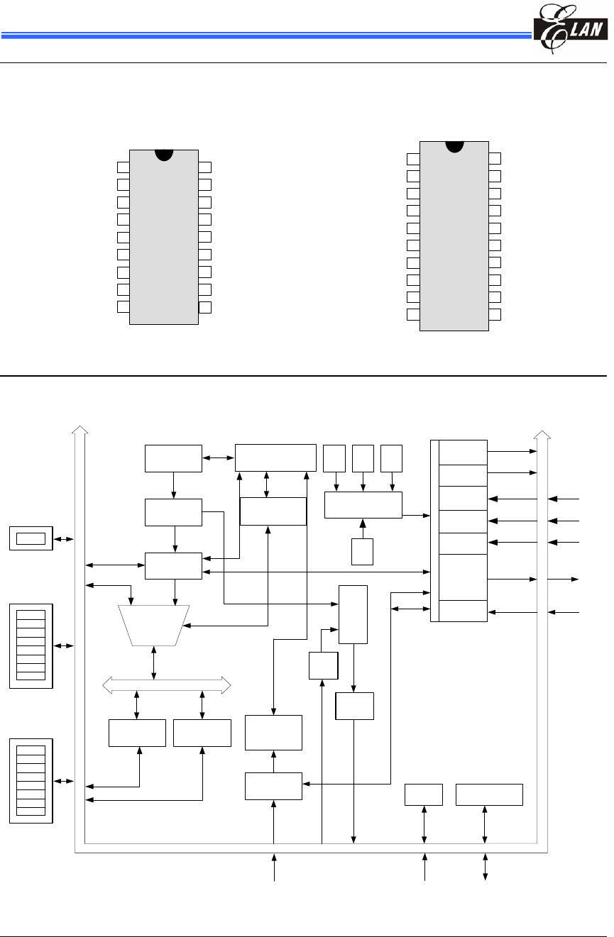
3 Pin Assignment
(1) 18-Pin DIP/SOP
P52/ADC2
P53/ADC3
P54/TCC/VREF
/RESET
Vss
P60//INT
P61/TCCA
P62/TCCB
P63/TCCC
P55/OSCI
P70/OSCO
VDD
P67/IR OUT
P65/CIN+
EM78P259NP
EM78P259NM
1
2
3
4
5
6
7
8
9
18
17
16
15
14
13
12
11
P64/CO
10
P66/CIN-
P50/ADC0
P51/ADC1
Fig. 3-1 EM78P259NP/M
(2) 20-Pin DIP/SOP/SSOP
1
2
3
4
5
6
7
8
9
10
20
19
18
17
16
15
14
13
12
11
P52/ADC2
P53/ADC3
P54/TCC/VREF
/RESET
Vss
P60//INT
P61/TCCA
P62/TCCB
P63/TCCC
P55/OSCI
P70/OSCO
VDD
P67/IR OUT
P65/CIN+
EM78P260N
P64/CO
P66/CIN-
P50/ADC0
P51/ADC1
P56 P57
Fig. 3-2 EM78P260NP/M/KM
4 Block Diagram
ROM
R3 (Status
Reg.)
ACC
Instruction
Decoder
Instruction
Register
ALU
PC
Interrupt
circuit
8-level stack
(13 bit)
Interrupt
control
register
Oscillation
Generation
RAM
Mux
Ext.
OSC.
R4
Ext.
RC
Int.
RC
Start-up
timer
WDT
TCCA
TCCB
TCCC
Infrared
remote
control
circuit
TCC
ADC Comparator
(CO) or OP
Ain0~3 Cin+ Cin- CO
TCCA
TCCC
TCCB
IR out
TCC
Ext INT
Reset
P6
P60
P67
P66
P65
P64
P63
P62
P61
P5
P50
P57
P56
P55
P54
P53
P52
P51
P7
P70
Fig. 4-1 EM78P259N/260N Functional Block Diagram

EM78P259N/260N
8-Bit Microprocessor with OTP ROM
Product Specification (V1.2) 05.18.2007 • 3
(This specification is subject to change without further notice)
5 Pin Description
5.1 EM78P259NP/M
Symbol Pin No. Type Function
P70 15 I/O
General purpose input/output pin
Default value after a power-on reset
P60~P67 6~13 I/O
General purpose input/output pin
Open-drain
Default value after a power-on reset
P50~P55 1~3
16~18 I/O
General purpose input/output pin
Pull-high/pull-down
Default value after a power-on reset
Wake up from sleep mode when the status of the pin changes
CIN-, CIN+
CO
12, 11
10
I
O
“-“ : the input pin of Vin- of the comparator
“+” : the input pin of Vin+ of the comparator
Pin CO is the comparator output
Defined by IOC80 <4:3>
OSCI 16 I
Crystal type: Crystal input terminal or external clock input pin
RC type: RC oscillator input pin
OSCO 15 I/O
Crystal type: Crystal input terminal or external clock input pin.
RC type: clock output with a duration of one instruction cycle
External clock signal input
/RESET 4 I
If set as /RESET and remains at logic low, the device will be
reset
Voltage on /RESET/Vpp must not exceed Vdd during normal
mode
TCC, TCCA,
TCCB, TCCC
3, 7,
8, 9 I
External Counter input
TCC is defined by CONT <5>
TCCA is defined by IOC80 <1>
TCCB is defined by IOC90 <5>
TCCC is defined by IOC90 <1>
ADC0~ADC3 1, 2,
17, 18 I Analog to Digital Converter
Defined by ADCON (R9) <1:0>
IR OUT 13 O
IR mode output pin, capable of driving and sinking
current=20mA when the output voltage drops to 0.7Vdd and
rise to0.3Vdd at Vdd=5V.
VREF 3 I
External reference voltage for ADC
Defined by ADCON (R9) <7>
/INT 6 I
External interrupt pin triggered by a falling or rising edge
Defined by CONT <7>
VDD 14 – Power supply
VSS 5 – Ground

EM78P259N/260N
8-Bit Microprocessor with OTP ROM
4 • Product Specification (V1.2) 05.18.2007
(This specification is subject to change without further notice)
5.2 EM78P260NP/M/KM
Symbol Pin No. Type Function
P70 16 I/O
General purpose input/output pin
Default value after a power-on reset
P60~P67 7~14 I/O
General purpose input/output pin
Open-drain
Default value after a power-on reset
P50~P57 1~4
17~20 I/O
General purpose input/output pin
Pull-high/pull-down
Default value after a power-on reset
Wake up from sleep mode when the status of the pin changes
CIN-, CIN+
CO
13, 12
11
I
O
“-“ : the input pin of Vin- of the comparator
“+” : the input pin of Vin+ of the comparator
Pin CO is the comparator output
Defined by IOC80 <4:3>
OSCI 17 I
Crystal type: Crystal input terminal or external clock input pin
RC type: RC oscillator input pin
OSCO 16 I/O
Crystal type: Crystal input terminal or external clock input pin.
RC type: clock output with a duration of one instruction cycle
External clock signal input
/RESET 5 I
If set as /RESET and remains at logic low, the device will be
reset
Voltage on /RESET/Vpp must not exceed Vdd during normal
mode
TCC, TCCA,
TCCB, TCCC
4, 8,
9, 10 I
External Timer/Counter input
TCC is defined by CONT <5>
TCCA is defined by IOC80 <1>
TCCB is defined by IOC90 <5>
TCCC is defined by IOC90 <1>
ADC0~ADC3 2, 3,
18, 19 I Analog to Digital Converter
Defined by ADCON (R9) <1:0>
IR OUT 14 O
IR mode output pin, capable of driving and sinking
current=20mA when the output voltage drops to 0.7Vdd and
rise to0.3Vdd at Vdd=5V.
VREF 4 I
External reference voltage for ADC
Defined by ADCON (R9) <7>
/INT 7 I
External interrupt pin triggered by a falling or rising edge
Defined by CONT <7>
VDD 15 – Power supply
VSS 6 – Ground
EM78P259N/260N
8-Bit Microprocessor with OTP ROM
Product Specification (V1.2) 05.18.2007 • 5
(This specification is subject to change without further notice)
6 Function Description
6.1 Operational Registers
6.1.1 R0 (Indirect Address Register)
R0 is not a physically implemented register. Its major function is to perform as an
indirect address pointer. Any instruction using R0 as a pointer, actually accesses the
data pointed by the RAM Select Register (R4).
6.1.2 R1 (Time Clock /Counter)
Increased by an external signal edge which is defined by the TE bit (CONT-4)
through the TCC pin, or by the instruction cycle clock.
Writable and readable as any other registers
The TCC prescaler counter (IOCC1) is assigned to TCC
The contents of the IOCC1 register is cleared –
• when a value is written to the TCC register.
• when a value is written to the TCC prescaler bits (Bits 3, 2, 1, 0 of the CONT
register)
• during power-on reset, /RESET, or WDT time out reset.
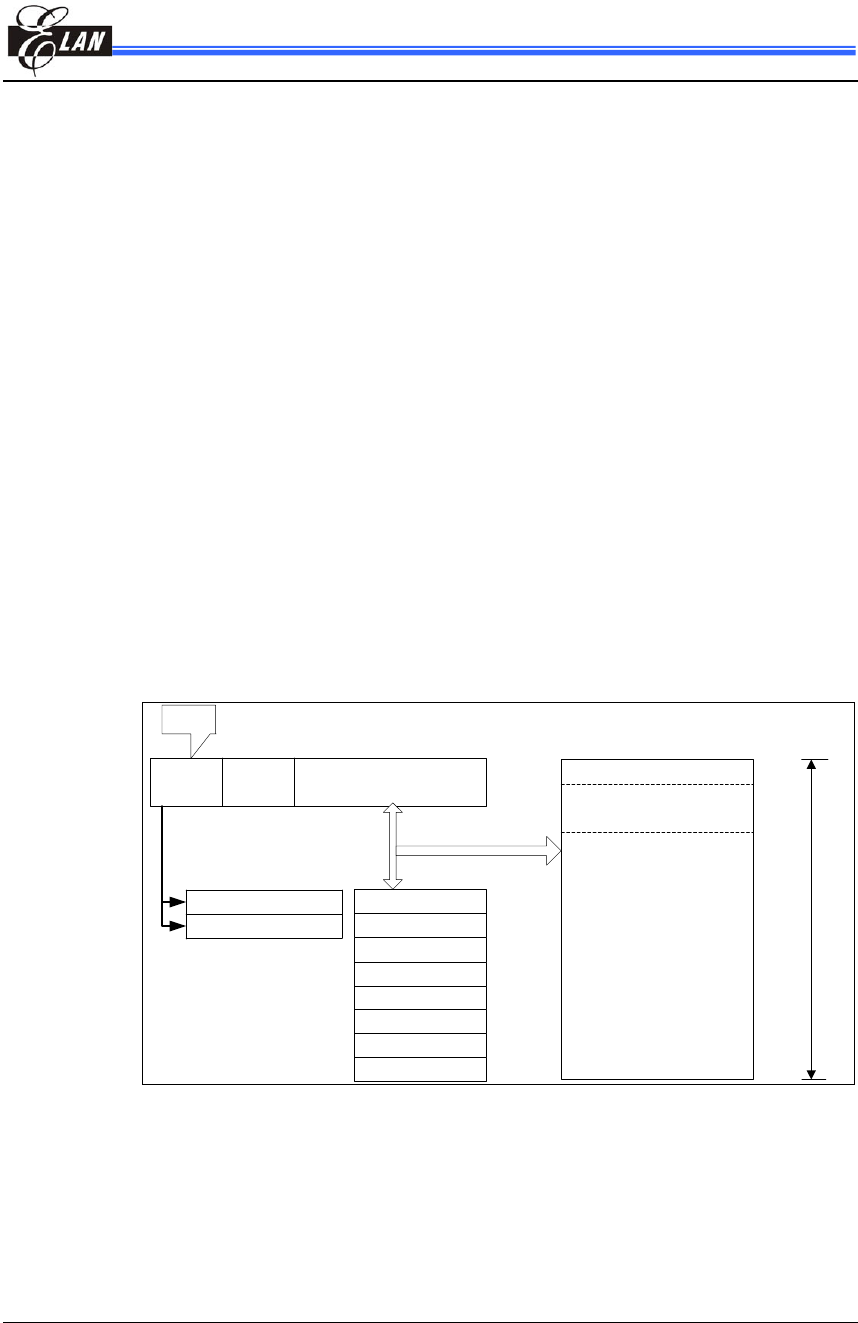
6.1.3 R2 (Program Counter) and Stack
A7 ~ A0
On-chip Program
Memory
000H
7FFH
003H
Hardware Interrupt Vector
User Memory Space
Reset Vector
A9 A8 A10
Stack Level 1
Stack Level 3
Stack Level 2
Stack Level 4
Stack Level 5
CALL
00 PAGE0 0000~03FF
01 PAGE1 0400~07FF
R3
RET
RETL
RETI
Stack Level 6
Stack Level 7
Stack Level 8
01EH
~
3FEH
Fig. 6-1 Program Counter Organization
R2 and hardware stacks are 12-bit wide. The structure is depicted in the table
under Section 6.1.3.1, Data Memory Configuration (subsequent page).
Generates 2K×13 bits on-chip ROM addresses to the relative programming
instruction codes. One program page is 1024 words long.
The contents of R2 are all set to "0"s when a reset condition occurs.

EM78P259N/260N
8-Bit Microprocessor with OTP ROM
6 • Product Specification (V1.2) 05.18.2007
(This specification is subject to change without further notice)
"JMP" instruction allows direct loading of the lower 10 program counter bits. Thus,
"JMP" allows PC to jump to any location within a page.
"CALL" instruction loads the lower 10 bits of the PC, and then PC+1 is pushed into
the stack. Thus, the subroutine entry address can be located anywhere within a
page.
"RET" ("RETL k", "RETI") instruction loads the program counter with the contents
of the top of stack.
"ADD R2, A" allows a relative address to be added to the current PC, and the ninth
and above bits of the PC will increase progressively.
"MOV R2, A" allows loading of an address from the "A" register to the lower 8 bits of
the PC, and the ninth and tenth bits (A8 ~ A9) of the PC will remain unchanged.
Any instruction (except “ADD R2,A”) that is written to R2 (e.g., "MOV R2, A", "BC
R2, 6", etc.) will cause the ninth bit and the tenth bit (A8 ~ A9) of the PC to remain
unchanged.
In the case of EM78P259N/260N, the most significant bit (A10) will be loaded with
the content of PS0 in the status register (R3) upon execution of a "JMP", "CALL", or
any other instructions set which write to R2.
All instructions are single instruction cycle (fclk/2 or fclk/4) except for the
instructions that are written to R2. Note that these instructions need one or two
instructions cycle as determined by Code Option Register CYES bit.

EM78P259N/260N
8-Bit Microprocessor with OTP ROM
Product Specification (V1.2) 05.18.2007 • 7
(This specification is subject to change without further notice)
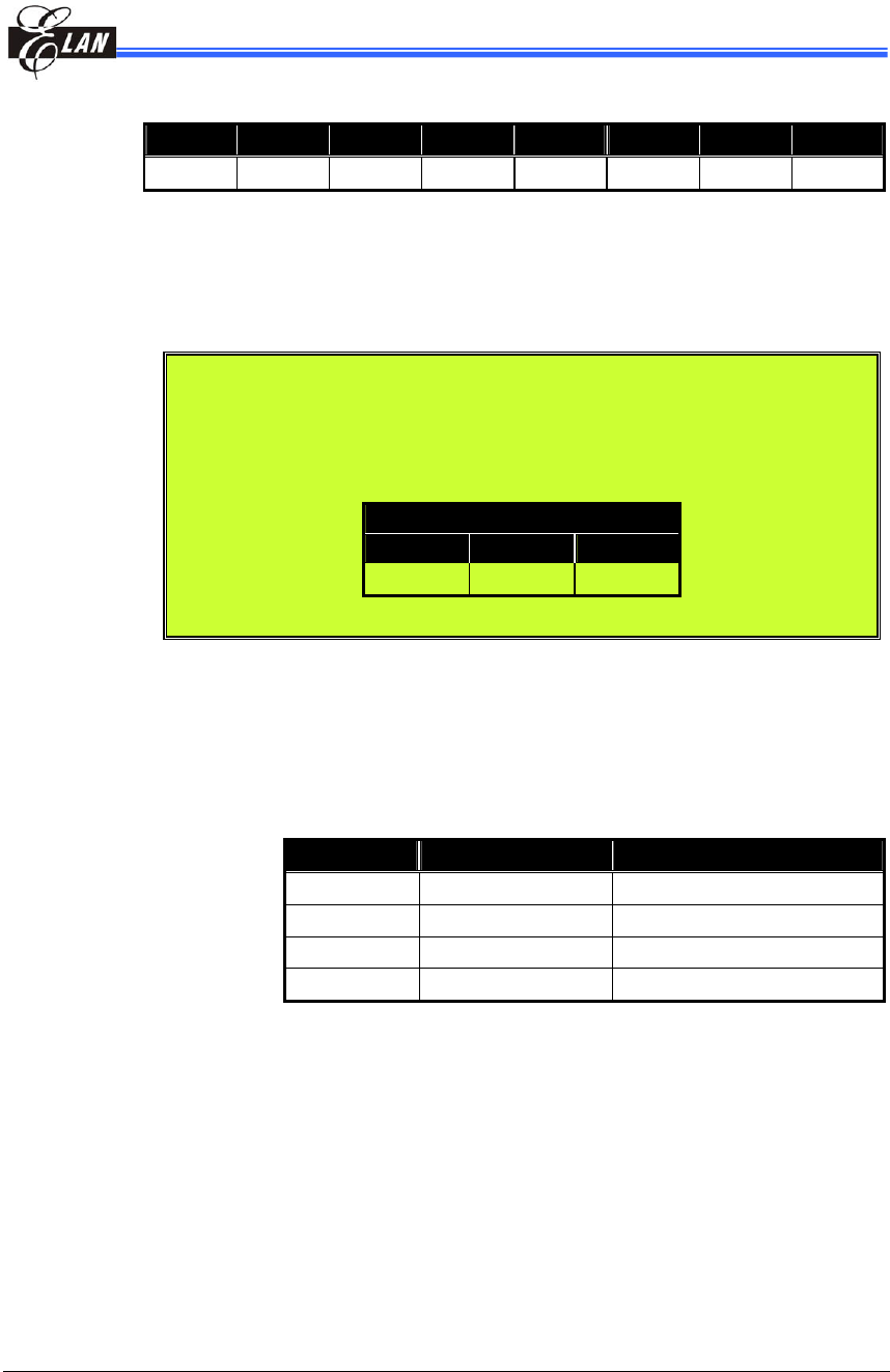
6.1.3.1 Data Memory Configuration
Address R PAGE registers IOCX0 PAGE registers
00 R0 (Indirect Addressing Register) Reserve
01 R1 (Time Clock Counter) CONT (Control Register)
02 R2 (Program Counter) Reserve
03 R3 (Status Register) Reserve
04 R4 (RAM Select Register) Reserve
05 R5 (Port 5) IOC50 (I/O Port Control Register)
06 R6 (Port 6) IOC60 (I/O Port Control Register)
07 R7 (Port 7) IOC70 (I/O Port Control Register)
08 (ADC Input Select Register
09
0A
0B IOCB0 (Pull-down Control
Register)
0C
0D
0E
0F IOCF0 (Interrupt Mask Register 1)
10
︰
1F
General Registers
20
:
3F
Bank 0 Bank 1
IOCX1 PAGE registers
IOC80 (Comparator and TCCA
Control Register)
IOC90 (TCCB and TCCC
Control Register)
IOCA0 (IR and TCCC Scale
Control Register)
IOCC0 (Open-drain Control
Register)
IOCD0 (Pull-high Control Register)
IOCE0 (WDT Control Register and
Interrupt Mask Register 2)
IOC51 (TCCA Counter)
IOC61 (TCCB LSB Counter)
IOC71 (TCCB HSB Counter)
IOC81 (TCCC Counter)
IOC91 (Low Time Register)
IOCA1 (High Time Register)
IOCB1 (High Time and Low Time
Scale control Register)
Reserve
Reserve
Reserve
Reserve
Reserve
Reserve
Reserve
Reserve
(ADC Control Register)
(ADC Offset Calibration
Register)
(The converted value
AD11~AD4 of ADC)
(The converted value
AD11~AD8 of ADC)
(The converted value
AD7~AD0 of ADC)
(Interrupt Status 2 and
Wake-up Control Register
(Interrupt Status Register 1)
R9
RA
RD
RE
RF
RB
RC
R8
IOCC1 (TCC Prescaler Control)

EM78P259N/260N
8-Bit Microprocessor with OTP ROM
8 • Product Specification (V1.2) 05.18.2007
(This specification is subject to change without further notice)
6.1.4 R3 (Status Register)
Bit 7 Bit 6 Bit 5 Bit 4 Bit 3 Bit 2 Bit 1 Bit 0
RST IOCS PS0 T P Z DC C
Bit 7 (RST): Bit of reset type
Set to “1” if wake-up from sleep on pin change, comparator status
change, or AD conversion completed. Set to “0” if wake-up from other
reset types
Bit 6 (IOCS): Select the Segment of IO control register
0 = Segment 0 (IOC50 ~ IOCF0) selected
1 = Segment 1 (IOC51 ~ IOCC1) selected
Bit 5 (PS0): Page select bits. PS0 is used to select a program memory page. When
executing a "JMP," "CALL," or other instructions which cause the
program counter to change (e.g., MOV R2, A), PS0 is loaded into the
11th bit of the program counter where it selects one of the available
program memory pages. Note that RET (RETL, RETI) instruction does
not change the PS0 bit. That is, the return address will always be back
to the page from where the subroutine was called, regardless of the
current PS0 bit setting.
PS0 Program Memory Page [Address]
0 Page 0 [000-3FF]
1 Page 1 [400-7FF]
Bit 4 (T): Time-out bit. Set to “1” by the "SLEP" and "WDTC" commands or during
power on; and reset to “0” by WDT time-out (see Section 6.5.2, The T
and P Status under STATUS Register for more details).
Bit 3 (P): Power-down bit. Set to “1” during power-on or by a "WDTC" command
and reset to “0” by a "SLEP" command (see Section 6.5.2, The T and P
Status under STATUS Register for more details).
Bit 2 (Z): Zero flag. Set to "1" if the result of an arithmetic or logic operation is
zero.
Bit 1 (DC): Auxiliary carry flag
Bit 0 (C): Carry flag
6.1.5 R4 (RAM Select Register)
Bit 7: Set to “0” all the time
Bit 6: Used to select Bank 0 or Bank 1 of the register
Bits 5~0: Used to select a register (Address: 00~0F, 10~3F) in indirect addressing
mode
See the table under Section 6.1.3.1, Data Memory Configuration for data memory
configuration.

EM78P259N/260N
8-Bit Microprocessor with OTP ROM
Product Specification (V1.2) 05.18.2007 • 9
(This specification is subject to change without further notice)
6.1.6 R5 ~ R6 (Port 5 ~ Port 6)
R5 & R6 are I/O registers
The upper 2 bits of R5 are fixed to “0” (if EM78P259N is selected).
Only the lower 6 bits of R5 are available (this applies to EM78P259N only as
EM78P260N can use all the bits)
6.1.7 R7 (Port 7)
Bit 7 6 5 4 3 2 1 0
EM78P259N/260N ‘0’ ‘0’ ‘0’ ‘0’ ‘0’ ‘0’ ‘0’ I/O
ICE259N C3 C2 C1 C0 RCM1 RCM0 ‘0’ I/O
Note: R7 is an I/O register
For EM78P259N/260N, only the lower 1 bit of R7 is available.
Bit 7 ~ Bit 2:
[With EM78P259N/260N]: Unimplemented, read as ‘0’.
[With Simulator (C3~C0, RCM1, & RCM0)]: are IRC calibration bits in IRC oscillator
mode. Under IRC oscillator mode of ICE259N simulator,
these are the IRC mode selection bits and IRC calibration bits.
Bit 7 ~ Bit 4 (C3 ~ C0): Calibrator of internal RC mode
C3 C2 C1 C0 Frequency (MHz)
0 0 0 0 (1-36%) x F
0 0 0 1 (1-31.5%) x F
0 0 1 0 (1-27%) x F
0 0 1 1 (1-22.5%) x F
0 1 0 0 (1-18%) x F
0 1 0 1 (1-13.5%) x F
0 1 1 0 (1-9%) x F
0 1 1 1 (1-4.5%) x F
1 1 1 1 F (default)
1 1 1 0 (1+4.5%) x F
1 1 0 1 (1+9%) x F
1 1 0 0 (1+135%) x F
1 0 1 1 (1+18%) x F
1 0 1 0 (1+22.5%) x F
1 0 0 1 (1+27%) x F
1 0 0 0 (1+31.5%) x F
1. Frequency values shown are theoretical and taken at an instance of
a high frequency mode. Hence, frequency values are shown for
reference only. Definite values depend on the actual process.
2. Similar way of calculation is also applicable to low frequency mode.

EM78P259N/260N
8-Bit Microprocessor with OTP ROM
10 • Product Specification (V1.2) 05.18.2007
(This specification is subject to change without further notice)
Bit 3 & Bit 2 (RCM1, RCM0): IRC mode selection bits
RCM 1 RCM 0 Frequency (MHz)
1 1 4 (default)
1 0 8
0 1 1
0 0 455kHz
6.1.8 R8 (AISR: ADC Input Select Register)
The AISR register individually defines the pins of Port 5 as analog input or as digital I/O.
Bit 7 Bit 6 Bit 5 Bit 4 Bit 3 Bit 2 Bit 1 Bit 0
– – – – ADE3 ADE2 ADE1 ADE0
Bit 7 ~ Bit 4: Not used
Bit 3 (ADE3): AD converter enable bit of P53 pin
0 = Disable ADC3, P53 functions as I/O pin
1 = Enable ADC3 to function as analog input pin
Bit 2 (ADE2): AD converter enable bit of P52 pin
0 = Disable ADC2, P52 functions as I/O pin
1 = Enable ADC2 to function as analog input pin
Bit 1 (ADE1): AD converter enable bit of P51 pin
0 = Disable ADC1, P51 functions as I/O pin
1 = Enable ADC1 to function as analog input pin
Bit 0 (ADE0): AD converter enable bit of P50 pin.
0 = Disable ADC0, P50 functions as I/O pin
1 = Enable ADC0 to function as analog input pin
EM78P259N/260N
8-Bit Microprocessor with OTP ROM
Product Specification (V1.2) 05.18.2007 • 11
(This specification is subject to change without further notice)
6.1.9 R9 (ADCON: ADC Control Register)
Bit 7 Bit 6 Bit 5 Bit 4 Bit 3 Bit 2 Bit 1 Bit 0
VREFS CKR1 CKR0 ADRUN ADPD – ADIS1 ADIS0
Bit 7 (VREFS): Input source of the Vref of the ADC
0 = The Vref of the ADC is connected to Vdd (default value), and the
P54/VREF pin carries out the function of P54
1 = The Vref of the ADC is connected to P54/VREF
NOTE
The P54/TCC/VREF pin cannot be applied to TCC and VREF at the same time.
If P54/TCC/VREF functions as VREF analog input pin, then CONT Bit 5 “TS”
must be “0.”
The P54/TCC/VREF pin priority is as follows:
Bit 6 & Bit 5 (CKR1 & CKR0): Prescaler of oscillator clock rate of ADC
00 = 1: 16 (default value)
01 = 1: 4
10 = 1: 64
11 = 1: WDT ring oscillator frequency
CKR1:CKR0 Operation Mode Max. Operation Frequency
00 Fosc/16 4 MHz
01 Fosc/4 1 MHz
10 Fosc/64 16 MHz
11 Internal RC –
Bit 4 (ADRUN): ADC starts to RUN.
0 = Reset upon completion of the conversion. This bit cannot be
reset through software
1 = AD conversion is started. This bit can be set by software.
Bit 3 (ADPD): ADC Power-down mode
0 = Switch off the resistor reference to conserve power even while the
CPU is operating
1 = ADC is operating
Bit 2: Not used
P53/TCC/VREF Pin Priority
High Medium Low
VREF TCC P54
EM78P259N/260N
8-Bit Microprocessor with OTP ROM
12 • Product Specification (V1.2) 05.18.2007
(This specification is subject to change without further notice)
Bit 1 ~ Bit 0 (ADIS1 ~ADIS0): Analog Input Select
00 = ADIN0/P50
01 = ADIN1/P51
10 = ADIN2/P52
11 = ADIN3/P53
These bits can only be changed when the ADIF bit (see Section
6.1.14, RE (Interrupt Status 2 & Wake-up Control Register)) and the
ADRUN bit are both LOW.
6.1.10 RA (ADOC: ADC Offset Calibration Register)
Bit 7 Bit 6 Bit 5 Bit 4 Bit 3 Bit 2 Bit 1 Bit 0
CALI SIGN VOF[2] VOF[1] VOF[0] “0” “0” “0”
Bit 7 (CALI): Calibration enable bit for ADC offset
0 = Calibration disable
1 = Calibration enable
Bit 6 (SIGN): Polarity bit of offset voltage
0 = Negative voltage
1 = Positive voltage
Bit 5 ~ Bit 3 (VOF[2] ~ VOF[0]): Offset voltage bits
VOF[2] VOF[1] VOF[0] EM78P259N/260N ICE259N
0 0 0 0LSB 0LSB
0 0 1 2LSB 1LSB
0 1 0 4LSB 2LSB
0 1 1 6LSB 3LSB
1 0 0 8LSB 4LSB
1 0 1 10LSB 5LSB
1 1 0 12LSB 6LSB
1 1 1 14LSB 7LSB
Bit 2 ~ Bit 0: Unimplemented, read as ‘0’
6.1.11 RB (ADDATA: Converted Value of ADC)
Bit 7 Bit 6 Bit 5 Bit 4 Bit 3 Bit 2 Bit 1 Bit 0
AD11 AD10 AD9 AD8 AD7 AD6 AD5 AD4
When AD conversion is completed, the result is loaded into the ADDATA. The ADRUN
bit is cleared, and the ADIF (see Section 6.1.14, RE (Interrupt Status 2 & Wake-up
Control Register)) is set.
RB is read only.

EM78P259N/260N
8-Bit Microprocessor with OTP ROM
Product Specification (V1.2) 05.18.2007 • 13
(This specification is subject to change without further notice)
6.1.12 RC (ADDATA1H: Converted Value of ADC)
Bit 7 Bit 6 Bit 5 Bit 4 Bit 3 Bit 2 Bit 1 Bit 0
“0” “0” “0” “0” AD11 AD10 AD9 AD8
When AD conversion is completed, the result is loaded into the ADDATA1H. The
ADRUN bit is cleared, and the ADIF (see Section 6.1.14, RE (Interrupt Status 2 &
Wake-up Control Register)) is set.
RC is read only
6.1.13 RD (ADDATA1L: Converted Value of ADC)
Bit 7 Bit 6 Bit 5 Bit 4 Bit 3 Bit 2 Bit 1 Bit 0
AD7 AD6 AD5 AD4 AD3 AD2 AD1 AD0
When AD conversion is completed, the result is loaded into the ADDATA1L. The
ADRUN bit is cleared, and the ADIF (see Section 6.1.14, RE (Interrupt Status 2 &
Wake-up Control Register)) is set.
RD is read only
6.1.14 RE (Interrupt Status 2 & Wake-up Control Register)
Bit 7 Bit 6 Bit 5 Bit 4 Bit 3 Bit 2 Bit 1 Bit 0
– – ADIF CMPIF ADWE CMPWE ICWE -
Note: RE <5, 4> can be cleared by instruction but cannot be set
IOCE0 is the interrupt mask register
Reading RE will result to "logic AND" of RE and IOCE0
Bit 7 & Bit 6: Not used
Bit 5 (ADIF): Interrupt flag for analog to digital conversion. Set when AD
conversion is completed. Reset by software
0 = no interrupt occurs
1 = with interrupt request
Bit 4 (CMPIF): Comparator interrupt flag. Set when a change occurs in the output of
Comparator. Reset by software.
0 = no interrupt occurs
1 = with interrupt request
Bit 3 (ADWE): ADC wake-up enable bit
0 = Disable ADC wake-up
1 = Enable ADC wake-up
When AD Conversion enters sleep mode, this bit must be set to
“Enable“.

EM78P259N/260N
8-Bit Microprocessor with OTP ROM
14 • Product Specification (V1.2) 05.18.2007
(This specification is subject to change without further notice)
Bit 2 (CMPWE): Comparator wake-up enable bit
0 = Disable Comparator wake-up
1 = Enable Comparator wake-up
When Comparator enters sleep mode, this bit must be set to “Enable.“
Bit 1 (ICWE): Port 5 input change to wake-up status enable bit
0 = Disable Port 5 input change to wake-up status
1 = Enable Port 5 input change to wake-up status
When Port 5 change enters sleep mode, this bit must be set to
“Enable“.
Bit 0: Not implemented, read as ‘0’
6.1.15 RF (Interrupt Status 2 Register)
Bit 7 Bit 6 Bit 5 Bit 4 Bit 3 Bit 2 Bit 1 Bit 0
LPWTIF HPWTIF TCCCIF TCCBIF TCCAIF EXIF ICIF TCIF
Note: “ 1 ” means with interrupt request “ 0 ” means no interrupt occurs
RF can be cleared by instruction but cannot be set.
IOCF0 is the relative interrupt mask register.
Reading RF will result to "logic AND" of RF and IOCF0.
Bit 7 (LPWTIF): Internal low-pulse width timer underflow interrupt flag for IR/PWM
function. Reset by software.
Bit 6 (HPWTIF): Internal high-pulse width timer underflow interrupt flag for IR/PWM
function. Reset by software.
Bit 5 (TCCCIF): TCCC overflow interrupt flag. Set when TCCC overflows. Reset by
software.
Bit 4 (TCCBIF): TCCB overflow interrupt flag. Set when TCCC overflows. Reset by
software.
Bit 3 (TCCAIF): TCCA overflow interrupt flag. Set when TCCC overflows. Reset by
software.
Bit 2 (EXIF): External interrupt flag. Set by falling edge on /INT pin. Reset by
software.
Bit 1 (ICIF): Port 5 input status change interrupt flag. Set when Port 5 input
changes. Reset by software.
Bit 0 (TCIF): TCC overflow interrupt flag. Set when TCC overflows. Reset by
software.
6.1.16 R10 ~ R3F
All of these are 8-bit general-purpose registers.

EM78P259N/260N
8-Bit Microprocessor with OTP ROM
Product Specification (V1.2) 05.18.2007 • 15
(This specification is subject to change without further notice)
6.2 Special Purpose Registers
6.2.1 A (Accumulator)
Internal data transfer operation, or instruction operand holding usually involves the
temporary storage function of the Accumulator, which is not an addressable register.
6.2.2 CONT (Control Register)
Bit 7 Bit 6 Bit 5 Bit 4 Bit 3 Bit 2 Bit 1 Bit 0
INTE INT TS TE PSTE PST2 PST1 PST0
Note: The CONT register is both readable and writable
Bit 6 is read only.
Bit 7 (INTE): INT signal edge
0 = interrupt occurs at the rising edge on the INT pin
1 = interrupt occurs at the falling edge on the INT pin
Bit 6 (INT): Interrupt enable flag
0 = masked by DISI or hardware interrupt
1 = enabled by the ENI/RETI instructions
This bit is readable only.
Bit 5 (TS): TCC signal source
0 = internal instruction cycle clock. P54 is bi-directional I/O pin.
1 = transition on the TCC pin
Bit 4 (TE): TCC signal edge
0 = increment if the transition from low to high takes place on the TCC
pin
1 = increment if the transition from high to low takes place on the TCC
pin.
Bit 3 (PSTE): Prescaler enable bit for TCC
0 = prescaler disable bit. TCC rate is 1:1.
1 = prescaler enable bit. TCC rate is set as Bit 2 ~ Bit 0.
EM78P259N/260N
8-Bit Microprocessor with OTP ROM
16 • Product Specification (V1.2) 05.18.2007
(This specification is subject to change without further notice)
Bit 2 ~ Bit 0 (PST2 ~ PST0): TCC prescaler bits
PST2 PST1 PST0 TCC Rate
0 0 0 1:2
0 0 1 1:4
0 1 0 1:8
0 1 1 1:16
1 0 0 1:32
1 0 1 1:64
1 1 0 1:128
1 1 1 1:256
Note: Tcc time-out period [1/Fosc x prescaler x 256 (Tcc cnt) x 1 (CLK=2)]
Tcc time-out period [1/Fosc x prescaler x 256 (Tcc cnt) x 2 (CLK=4)]
6.2.3 IOC50 ~ IOC70 (I/O Port Control Register)
"1" puts the relative I/O pin into high impedance, while "0" defines the relative I/O
pin as output.
Only the lower 6 bits of IOC50 can be defined (this applies to EM78P259N only,
since EM78P260N can use all the bits).
Only the lower 1 bit of IOC70 can be defined, the other bits are not available.
IOC50, IOC60, and IOC70 registers are all readable and writable
6.2.4 IOC80 (Comparator and TCCA Control Register)
Bit 7 Bit 6 Bit 5 Bit 4 Bit 3 Bit 2 Bit 1 Bit 0
– – CMPOUT COS1 COS0 TCCAEN TCCATS TCCATE
Note: Bits 4~0 of the IOC80 register are both readable and writable
Bit 5 of the IOC80 register is read only.
Bit 7 & Bit 6: Not used
Bit 5 (CMPOUT): Result of the comparator output
This bit is read only.
Bit 4 & Bit 3 (COS1 & COS0): Comparator/OP Select bits
COS1 COS0 Function Description
0 0
Comparator and OP are not used. P64, P65, and P66 function as
normal I/O pins.
0 1 Acts as Comparator and P64 functions as normal I/O pin
1 0 Acts as Comparator and P64 functions as Comparator output pin (CO)
1 1 Acts as OP and P64 functions as OP output pin (CO)
Bit 2 (TCCAEN): TCCA enable bit
0 = disable TCCA
1 = enable TCCA as a counter

EM78P259N/260N
8-Bit Microprocessor with OTP ROM
Product Specification (V1.2) 05.18.2007 • 17
(This specification is subject to change without further notice)
Bit 1 (TCCATS): TCCA signal source
0 =: internal instruction cycle clock. P61 is a bi-directional I/O pin.
1 = transit through the TCCA pin
Bit 0 (TCCATE): TCCA signal edge
0 = increment if transition from low to high takes place on the
TCCA pin
1 = increment if transition from high to low takes place on the
TCCA pin
6.2.5 IOC90 (TCCB and TCCC Control Register)
Bit 7 Bit 6 Bit 5 Bit 4 Bit 3 Bit 2 Bit 1 Bit 0
TCCBHE TCCBEN TCCBTS TCCBTE – TCCCEN TCCCTS TCCCTE
Bit 7 (TCCBHE): Control bit is used to enable the most significant byte of counter
0 = Disable the most significant byte of TCCBH (default value)
TCCB is an 8-bit counter
1 = Enable the most significant byte of TCCBH
TCCB is a 16-bit counter
Bit 6 (TCCBEN): TCCB enable bit
0 = disable TCCB
1 = enable TCCB as a counter
Bit 5 (TCCBTS) TCCB signal source
0 = internal instruction cycle clock. P62 is a bi-directional I/O pin.
1 = transit through the TCCB pin
Bit 4 (TCCBTE): TCCB signal edge
0 = increment if the transition from low to high takes place on the
TCCB pin
1 = increment if the transition from high to low takes place on the
TCCB pin
Bit 3: Not used.
Bit 2 (TCCCEN): TCCC enable bit
0 = disable TCCC
1 = enable TCCC as a counter
Bit 1 (TCCCTS) TCCC signal source
0 = internal instruction cycle clock. P63 is a bi-directional I/O pin.
1 = transit through the TCCC pin
Bit 0 (TCCCTE): TCCC signal edge

EM78P259N/260N
8-Bit Microprocessor with OTP ROM
18 • Product Specification (V1.2) 05.18.2007
(This specification is subject to change without further notice)
0 = increment if the transition from low to high takes place on the
TCCC pin
1 = increment if the transition from high to low takes place on the
TCCC pin
6.2.6 IOCA0 (IR and TCCC Scale Control Register)
Bit 7 Bit 6 Bit 5 Bit 4 Bit 3 Bit 2 Bit 1 Bit 0
TCCCSE TCCCS2 TCCCS1 TCCCS0 IRE HF LGP IROUTE
Bit 7 (TCCCSE): Scale enable bit for TCCC
An 8-bit counter is provided as scaler for TCCC and IR-Mode. When
in IR-Mode, TCCC counter scale uses the low time segments of the
pulse generated by Fcarrier frequency modulation (see Fig. 6-11 in
Section 6.8.2, Function Description).
0 = scale disable bit, TCCC rate is 1:1
1 = scale enable bit, TCCC rate is set as Bit 6 ~ Bit 4

EM78P259N/260N
8-Bit Microprocessor with OTP ROM
Product Specification (V1.2) 05.18.2007 • 19
(This specification is subject to change without further notice)
Bit 6 ~ Bit 4 (TCCCS2 ~ TCCCS0): TCCC scale bits
The TCCCS2 ~ TCCCS0 bits of the IOCA0 register are used to
determine the scale ratio of TCCC as shown below:
TCCCS2 TCCCS1 TCCCS0 TCCC Rate
0 0 0 1:2
0 0 1 1:4
0 1 0 1:8
0 1 1 1:16
1 0 0 1:32
1 0 1 1:64
1 1 0 1:128
1 1 1 1:256
Bit 3 (IRE): Infrared Remote Enable bit
0 = Disable IRE, i.e., disable H/W Modulator Function. IROUT pin
fixed to high level and the TCCC is an Up Counter.
1 = Enable IRE, i.e., enable H/W Modulator Function. Pin 67 is
defined as IROUT. If HP=1, the TCCC counter scale uses the
low time segments of the pulse generated by Fcarrier frequency
modulation (see Fig. 6-11 in Section 6.8.2, Function
Description). When HP=0, the TCCC is an Up Counter.
Bit 2 (HF): High Frequency bit
0 = PWM application. IROUT waveform is achieved according to
high-pulse width timer and low-pulse width timer which
determines the high time width and low time width respectively
1 = IR application mode. The low time segments of the pulse
generated by Fcarrier frequency modulation (see Fig. 6-11 in
Section 6.8.2, Function Description)
Bit 1 (LGP): Long Pulse.
0 = high time register and low time register is valid
1 = high time register is ignored. A single pulse is generated.
Bit 0 (IROUTE): Control bit to define the P67 (IROUT) pin function
0 = P67 is defined as bi-directional I/O pin
1 = P67 is defined as IROUT. Under this condition, the I/O control
bit of P67 (Bit 7 of IOC60) must be set to “0”

EM78P259N/260N
8-Bit Microprocessor with OTP ROM
20 • Product Specification (V1.2) 05.18.2007
(This specification is subject to change without further notice)
6.2.7 IOCB0 (Pull-down Control Register)
Bit 7 Bit 6 Bit 5 Bit 4 Bit 3 Bit 2 Bit 1 Bit 0
/PD57 /PD56 /PD55 /PD54 /PD53 /PD52 /PD51 /PD50
Note: The IOCB0 register is both readable and writable
Bit 7 (/PD57): Control bit used to enable the pull-down function of the P57 pin
(applicable to EM78P260N only)
0 = Enable internal pull-down
1 = Disable internal pull-down
Bit 6 (/PD56): Control bit used to enable the pull-down function of the P56 pin
(applicable to EM78P260N only)
Bit 5 (/PD55): Control bit used to enable the pull-down function of the P55 pin
Bit 4 (/PD54): Control bit used to enable the pull-down function of the P54 pin
Bit 3 (/PD53): Control bit used to enable the pull-down function of the P53 pin
Bit 2 (/PD52): Control bit used to enable the pull-down function of the P52 pin
Bit 1 (/PD51): Control bit used to enable the pull-down function of the P51 pin
Bit 0 (/PD50): Control bit used to enable the pull-down function of the P50 pin.
6.2.8 IOCC0 (Open-Drain Control Register)
Bit 7 Bit 6 Bit 5 Bit 4 Bit 3 Bit 2 Bit 1 Bit 0
/OD67 /OD66 /OD65 /OD64 /OD63 /OD62 /OD61 /OD60
Note: The IOCC0 register is both readable and writable
Bit 7 (/OD67): Control bit used to enable the open-drain output of the P67 pin
0 = Enable open-drain output
1 = Disable open-drain output
Bit 6 (/OD66): Control bit used to enable the open-drain output of the P66 pin
Bit 5 (/OD65): Control bit used to enable the open-drain output of the P65 pin
Bit 4 (/OD64): Control bit used to enable the open-drain output of the P64 pin
Bit 3 (/OD63): Control bit used to enable the open-drain output of the P63 pin
Bit 2 (/OD62): Control bit used to enable the open-drain output of the P62 pin
Bit 1 (/OD61): Control bit used to enable the open-drain output of the P61 pin
Bit 0 (/OD60): Control bit used to enable the open-drain output of the P60 pin

EM78P259N/260N
8-Bit Microprocessor with OTP ROM
Product Specification (V1.2) 05.18.2007 • 21
(This specification is subject to change without further notice)
6.2.9 IOCD0 (Pull-high Control Register)
Bit 7 Bit 6 Bit 5 Bit 4 Bit 3 Bit 2 Bit 1 Bit 0
/PH57 /PH56 /PH55 /PH54 /PH53 /PH52 /PH51 /PH50
Note: The IOCD0 register is both readable and writable
Bit 7 (/PH57): Control bit is used to enable the pull-high of the P57 pin (applicable to
EM78P260N only).
0 = Enable internal pull-high;
1 = Disable internal pull-high.
Bit 6 (/PH56): Control bit used to enable the pull-high function of the P56 pin
(applicable to EM78P260N only).
Bit 5 (/PH55): Control bit used to enable the pull-high function of the P55 pin.
Bit 4 (/PH54): Control bit used to enable the pull-high function of the P54 pin.
Bit 3 (/PH53): Control bit used to enable the pull-high function of the P53 pin.
Bit 2 (/PH52): Control bit used to enable the pull-high function of the P52 pin.
Bit 1 (/PH51): Control bit used to enable the pull-high function of the P51 pin.
Bit 0 (/PH50): Control bit used to enable the pull-high function of the P50 pin.
6.2.10 IOCE0 (WDT Control & Interrupt Mask Registers 2)
Bit 7 Bit 6 Bit 5 Bit 4 Bit 3 Bit 2 Bit 1 Bit 0
WDTE EIS ADIE CMPIE PSWE PSW2 PSW1 PSW0
Bit 7 (WDTE): Control bit used to enable Watchdog Timer
0 = Disable WDT
1 = Enable WDT
WDTE is both readable and writable
Bit 6 (EIS): Control bit used to define the function of the P60 (/INT) pin
0 = P60, bi-directional I/O pin
1 = /INT, external interrupt pin. In this case, the I/O control bit of P60
(Bit 0 of IOC60) must be set to "1"
NOTE
■ When EIS is "0," the path of /INT is masked. When EIS is "1," the status of /INT pin
can also be read by way of reading Port 6 (R6). Refer to Fig. 6-4 (I/O Port and I/O
Control Register Circuit for P60 (/INT)) under Section 6.4 (I/O Ports).
■ EIS is both readable and writable.

EM78P259N/260N
8-Bit Microprocessor with OTP ROM
22 • Product Specification (V1.2) 05.18.2007
(This specification is subject to change without further notice)
Bit 5 (ADIE): ADIF interrupt enable bit
0 = disable ADIF interrupt
1 = enable ADIF interrupt
Bit 4 (CMPIE): CMPIF interrupt enable bit.
0 = disable CMPIF interrupt
1 = enable CMPIF interrupt
Bit 3 (PSWE): Prescaler enable bit for WDT
0 = prescaler disable bit, WDT rate is 1:1
1 = prescaler enable bit, WDT rate is set as Bit 2 ~ Bit 0
Bit 2 ~ Bit 0 (PSW2 ~ PSW0): WDT prescaler bits
PSW2 PSW1 PSW0 WDT Rate
0 0 0 1:2
0 0 1 1:4
0 1 0 1:8
0 1 1 1:16
1 0 0 1:32
1 0 1 1:64
1 1 0 1:128
1 1 1 1:256
6.2.11 IOCF0 (Interrupt Mask Register)
Bit 7 Bit 6 Bit 5 Bit 4 Bit 3 Bit 2 Bit 1 Bit 0
LPWTIE HPWTIE TCCCIE TCCBIE TCCAIE EXIE ICIE TCIE
NOTE
■ The IOCF0 register is both readable and writable
■ Individual interrupt is enabled by setting its associated control bit in the IOCF0 and
in IOCE0 Bit 4 & 5 to "1".
■ Global interrupt is enabled by the ENI instruction and is disabled by the DISI
instruction. Refer to Fig. 6-8 (Interrupt Input Circuit) under Section 6.6 (Interrupt).
Bit 7 (LPWTIE): LPWTIF interrupt enable bit
0 = Disable LPWTIF interrupt
1 = Enable LPWTIF interrupt
Bit 6 (HPWTIE): HPWTIF interrupt enable bit
0 = Disable HPWTIF interrupt
1 = Enable HPWTIF interrupt

EM78P259N/260N
8-Bit Microprocessor with OTP ROM
Product Specification (V1.2) 05.18.2007 • 23
(This specification is subject to change without further notice)
Bit 5 (TCCCIE): TCCCIF interrupt enable bit
0 = Disable TCCCIF interrupt
1 = Enable TCCCIF interrupt
Bit 4 (TCCBIE): TCCBIF interrupt enable bit
0 = Disable TCCBIF interrupt
1 = Enable TCCBIF interrupt
Bit 3 (TCCAIE): TCCAIF interrupt enable bit
0 = Disable TCCAIF interrupt
1 = Enable TCCAIF interrupt
Bit 2 (EXIE): EXIF interrupt enable bit
0 = Disable EXIF interrupt
1 = Enable EXIF interrupt
Bit 1 (ICIE): ICIF interrupt enable bit
0 = Disable ICIF interrupt
1 = Enable ICIF interrupt
Bit 0 (TCIE): TCIF interrupt enable bit.
0 = Disable TCIF interrupt
1 = Enable TCIF interrupt
6.2.12 IOC51 (TCCA Counter)
The IOC51 (TCCA) is an 8-bit clock counter. It can be read, written, and cleared on
any reset condition and is an Up Counter.
NOTE
■ TCCA timeout period [1/Fosc x (256-TCCA cnt) x 1(CLK=2)]
■ TCCA timeout period [1/Fosc x (256-TCCA cnt) x 2(CLK=4)]
6.2.13 IOC61 (TCCB Counter)
The IOC61 (TCCB) is an 8-bit clock counter for the least significant byte of TCCBX
(TCCB). It can be read, written, and cleared on any reset condition and is an Up
Counter.

EM78P259N/260N
8-Bit Microprocessor with OTP ROM
24 • Product Specification (V1.2) 05.18.2007
(This specification is subject to change without further notice)
6.2.14 IOC71 (TCCBH/MSB Counter)
The IOC71 (TCCBH) is an 8-bit clock counter for the most significant byte of TCCBX
(TCCBH). It can be read, written, and cleared on any reset condition.
When TCCBHE (IOC90) is “0,” then TCCBH is disabled. When TCCBHE is”1,” then
TCCB is a 16-bit length counter.
NOTE
When TCCBH is Disabled:
■ TCCB time-out period [1/Fosc x ( 256 - TCCB cnt ) x 1(CLK=2)]
■ TCCB time-out period [1/Fosc x ( 256 - TCCB cnt ) x 2(CLK=4)]
When TCCBH is Enabled:
■ TCCB time-out period {1/Fosc x [ 65536 - (TCCBH * 256 + TCCB cnt)] x 1(CLK=2)}
■ TCCB time-out period {1/Fosc x [ 65536 - (TCCBH * 256 + TCCB cnt)] x 2(CLK=4)}
6.2.15 IOC81 (TCCC Counter)
The IOC81 (TCCC) is an 8-bit clock counter that can be extended to 16-bit counter.
It can be read, written, and cleared on any reset condition.
If HF (Bit 2 of IOCA0) = 1 and IRE (Bit 3 of IOCA0) = 1, TCCC counter scale uses the
low time segments of the pulse generated by Fcarrier frequency modulation (see Fig.
6-12 in Section 6.8.2, Function Description). Then TCCC value will be TCCC predict
value.
When HP = 0 or IRE = 0, the TCCC is an Up Counter.
NOTE
In TCCC Up Counter mode:
■ TCCC time-out period [1/Fosc x scaler (IOCA0) x (256-TCCC cnt) x 1(CLK=2)]
■ TCCC time-out period [1/Fosc x scaler (IOCA0) x (256-TCCC cnt) x 2(CLK=4)]
When HP = 1 and IRE = 1, TCCC counter scale uses the low time segments of the
pulse generated by Fcarrier frequency modulation.
NOTE
In IR mode:
■ Fcarrier = FT/ 2 { [1+decimal TCCC Counter value (IOC81)] * TCCC Scale
(IOCA0) }
■ FT is system clock: FT = Fosc/1 (CLK=2)
FT = Fosc/2 (CLK=4)

EM78P259N/260N
8-Bit Microprocessor with OTP ROM
Product Specification (V1.2) 05.18.2007 • 25
(This specification is subject to change without further notice)
6.2.16 IOC91 (Low Time Register)
The 8-bit Low time register controls the active or Low segment of the pulse.
The decimal value of its contents determines the number of oscillator cycles and
verifies that the IR OUT pin is active. The active period of IR OUT can be calculated as
follows:
NOTE
■ Low time width = { [1+decimal low time value (IOC91)] * Low time Scale(IOCB1) } /
FT
■ FT is system clock: FT = Fosc/1 (CLK=2)
FT = Fosc/2 (CLK=4)
When an interrupt is generated by the Low time down counter underflow (if enabled),
the next instruction will be fetched from Address 015H (Low time).
6.2.17 IOCA1 (High Time Register)
The 8-bit High time register controls the inactive or High period of the pulse.
The decimal value of its contents determine the number of oscillator cycles and verifies
that the IR OUT pin is inactive. The inactive period of IR OUT can be calculated as
follows:
NOTE
■ High time width = {[1+decimal high time value (IOCA1)] * High time Scale(IOCB1) }
/ FT
■ FT is system clock: FT=Fosc/1(CLK=2)
FT=Fosc/2(CLK=4)
When an interrupt is generated by the High time down counter underflow (if enabled),
the next instruction will be fetched from Address 012H (High time).
6.2.18 IOCB1 High/Low Time Scale Control Register)
Bit 7 Bit 6 Bit 5 Bit 4 Bit 3 Bit 2 Bit 1 Bit 0
HTSE HTS2 HTS1 HTS0 LTSE LTS2 LTS1 LTS0
Bit 7 (HTSE): High time scale enable bit.
0 = scale disable bit, High time rate is 1:1
1 = scale enable bit, High time rate is set as Bit 6~Bit 4.
EM78P259N/260N
8-Bit Microprocessor with OTP ROM
26 • Product Specification (V1.2) 05.18.2007
(This specification is subject to change without further notice)
Bit 6 ~ Bit 4 (HTS2 ~ HTS0): High time scale bits:
HTS2 HTS1 HTS0 High time Rate
0 0 0 1:2
0 0 1 1:4
0 1 0 1:8
0 1 1 1:16
1 0 0 1:32
1 0 1 1:64
1 1 0 1:128
1 1 1 1:256
Bit 3 (LTSE): Low time scale enable bit.
0 = scale disable bit, Low time rate is 1:1
1 = scale enable bit, Low time rate is set as Bit 2~Bit 0.
Bit 2 ~ Bit 0 (LTS2 ~ LTS0): Low time scale bits:
LTS2 LTS1 LTS0 Low time Rate
0 0 0 1:2
0 0 1 1:4
0 1 0 1:8
0 1 1 1:16
1 0 0 1:32
1 0 1 1:64
1 1 0 1:128
1 1 1 1:256
6.2.19 IOCC1 (TCC Prescaler Counter)
The TCC prescaler counter can be read and written to.
PST2 PST1 PST0 Bit 7 Bit 6 Bit 5 Bit 4 Bit 3 Bit 2 Bit 1 Bit 0 TCC
Rate
0 0 0 - - - - - - - V 1:2
0 0 1 - - - - - - V V 1:4
0 1 0 - - - - - V V V 1:8
0 1 1 - - - - V V V V 1:16
1 0 0 - - - V V V V V 1:32
1 0 1 - - V V V V V V 1:64
1 1 0 - V V V V V V V 1:128
1 1 1 V V V V V V V V 1:256
V = valid value
The TCC prescaler counter is assigned to TCC (R1).
The contents of the IOCC1 register are cleared when one of the following occurs:
a value is written to TCC register
a value is written to TCC prescaler bits (Bits 3, 2, 1, 0 of CONT)
power-on reset, /RESET
WDT time-out reset

EM78P259N/260N
8-Bit Microprocessor with OTP ROM
Product Specification (V1.2) 05.18.2007 • 27
(This specification is subject to change without further notice)
6.3 TCC/WDT and Prescaler
There are two 8-bit counters available as prescalers that can be extended to 16-bit
counter for the TCC and WDT respectively. The PST2 ~ PST0 bits of the CONT
register are used to determine the ratio of the TCC prescaler, and the PWR2 ~ PWR0
bits of the IOCE0 register are used to determine the WDT prescaler. The prescaler
counter is cleared by the instructions each time such instructions are written into TCC.
The WDT and prescaler will be cleared by the “WDTC” and “SLEP” instructions. Fig.
6-2 (next page) depicts the block diagram of TCC/WDT.
TCC (R1) is an 8-bit timer/counter. The TCC clock source can be an internal clock or
external signal input (edge selectable from the TCC pin). If TCC signal source is from
the internal clock, TCC will increase by 1 at every instruction cycle (without prescaler).
Referring to Fig. 6-2, CLK=Fosc/2 or CLK=Fosc/4 is dependent to the Code Option bit
<CLKS>. CLK=Fosc/2 if the CLKS bit is "0," and CLK=Fosc/4 if the CLKS bit is "1." If
TCC signal source is from an external clock input, TCC will increase by 1 at every
falling edge or rising edge of the TCC pin. The TCC pin input time length (kept in High
or Low level) must be greater than 1CLK.
NOTE
The internal TCC will stop running when sleep mode occurs. However, during AD
conversion, when TCC is set to “SLEP” instruction, if the ADWE bit of the RE register
is enabled, the TCC will keep on running
The watchdog timer is a free running on-chip RC oscillator. The WDT will keep on
running even when the oscillator driver has been turned off (i.e., in sleep mode).
During normal operation or sleep mode, a WDT time-out (if enabled) will cause the
device to reset. The WDT can be enabled or disabled at any time during normal mode
through software programming. Refer to WDTE bit of IOCE0 register (Section 6.2.10
IOCE0 (WDT Control & Interrupt Mask Registers 2). With no prescaler, the WDT
time-out period is approximately 18ms1 or or 4.5ms2.
1 VDD=5V, WDT time-out period = 16.5ms ± 30%
VDD=3V, WDT time-out period = 18ms ± 30%
2 VDD=5V, WDT time-out period = 4.2ms ± 30%
VDD=3V, WDT time-out period = 4.5ms ± 30%
EM78P259N/260N
8-Bit Microprocessor with OTP ROM
28 • Product Specification (V1.2) 05.18.2007
(This specification is subject to change without further notice)
8-Bit counterWDT
Prescaler8 to 1 MUX
WDT Time out
WDTE
(IOCE0)
TCC Pin MUX
1CLK (Fosc/1)
8-Bit Counter (IOCC1)
8 to 1 MUX
TE (CONT)
Data Bus
TCC overflow
interrupt
TS (CONT)
TCC (R1)
0
1
PSW2~0
(IOCE0)
Prescaler
PSR2~0
(CONT)
2 CLK (Fosc/2)
Fig. 6-2 TCC and WDT Block Diagram
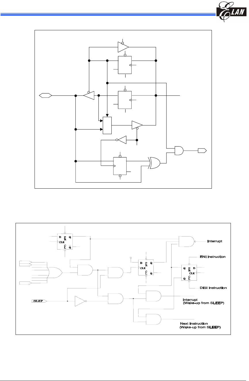
6.4 I/O Ports
The I/O registers (Port 5, Port 6, and Port 7) are bi-directional tri-state I/O ports. Port 5
is pulled-high and pulled-down internally by software. Likewise, P6 has its open-drain
output through software. Port 5 features an input status changed interrupt (or wake-up)
function. Each I/O pin can be defined as "input" or "output" pin by the I/O control
register (IOC5 ~ IOC7). The I/O registers and I/O control registers are both readable
and writable. The I/O interface circuits for Port 5, Port 6, and Port7 are illustrated in
Figures 6-3, 6-4, 6-5, & 6-6 (see next page).
EM78P259N/260N
8-Bit Microprocessor with OTP ROM
Product Specification (V1.2) 05.18.2007 • 29
(This specification is subject to change without further notice)
PCWR
PCRD
PDWR
PDRD
IOD
0
1
M
U
X
PORT Q
Q
_
D
D
Q
Q
_
CLK
P
R
C
L
CLK
P
R
C
L
Note: Open-drain is not shown in the figure.
Fig. 6-3 I/O Port and I/O Control Register Circuit for Port 6 and Port 7
PCRD
IOD
PCWR
PDWR
PDRD
Bit 6 of IOCE
PORT
M
U
X
0
1
CLK
CLK
CLK
P
P
P
R
R
R
C
L
L
L
C
C
Q
Q
Q
Q
Q
Q
D
D
D
_
_
_
INT
Note: Open-drain is not shown in the figure.
Fig. 6-4 I/O Port and I/O Control Register Circuit for P60 (/INT)
EM78P259N/260N
8-Bit Microprocessor with OTP ROM
30 • Product Specification (V1.2) 05.18.2007
(This specification is subject to change without further notice)
PCRD
M
U
X
IOD
0
1
PDRD
P50 ~ P57
PCWR
DQ
Q
_CLK
P
R
C
L
PDWR
DQ
Q
_CLK
P
R
C
L
P
R
C
L
CLK
DQ
Q
_
TI n
PORT
Note: Pull-high (down) is not shown in the figure.
Fig. 6-5 I/O Port and I/O Control Register Circuit for Port 50 ~ P57
TI 1
TI 8
IOCF.1
TI 0
RF.1
….
Fig. 6-6 Port 5 Block Diagram with Input Change Interrupt/Wake-up

EM78P259N/260N
8-Bit Microprocessor with OTP ROM
Product Specification (V1.2) 05.18.2007 • 31
(This specification is subject to change without further notice)
6.4.1 Usage of Port 5 Input Change Wake-up/Interrupt Function
(1) Wake-up (2) Wake-up and Interrupt
(a) Before Sleep (a) Before Sleep
1. Disable WDT 1. Disable WDT
2. Read I/O Port 5 (MOV R5,R5) 2. Read I/O Port 5 (MOV R5,R5)
3. Execute "ENI" or "DISI" 3. Execute "ENI" or "DISI"
4. Enable wake-up bit (Set RE ICWE =1) 4. Enable wake-up bit (Set RE ICWE =1)
5. Execute "SLEP" instruction 5. Enable interrupt (Set IOCF0 ICIE =1)
(b) After wake-up 6. Execute "SLEP" instruction
→ Next instruction (b) After wake-up
1. IF "ENI" → Interrupt vector (006H)
2. IF "DISI" → Next instruction
(3) Interrupt
(a) Before Port 5 pin change
1. Read I/O Port 5 (MOV R5,R5)
2. Execute "ENI" or "DISI"
3. Enable interrupt (Set IOCF0 ICIE =1)
(b) After Port 5 pin changed (interrupt)
1. IF "ENI" → Interrupt vector (006H)
2. IF "DISI" → Next instruction
6.5 Reset and Wake-up
6.5.1 Reset and Wake-up Operation
A reset is initiated by one of the following events:
1. Power-on reset
2. /RESET pin input "low"
3. WDT time-out (if enabled).
The device is kept under reset condition for a period of approximately 18ms3 (except in
LXT mode) after the reset is detected. When in LXT mode, the reset time is 500ms.
Two choices (18ms3 or 4.5ms4) are available for WDT-time out period. Once a reset
occurs, the following functions are performed (the initial Address is 000h):
The oscillator continues running, or will be started (if in sleep mode)
The Program Counter (R2) is set to all "0"
3 VDD=5V, WDT Time-out period = 16.5ms ± 30%.
VDD=3V, WDT Time-out period = 18ms ± 30%.
4 VDD=5V, WDT Time-out period = 4.2ms ± 30%.
VDD=3V, WDT Time-out period = 4.5ms ± 30%.

EM78P259N/260N
8-Bit Microprocessor with OTP ROM
32 • Product Specification (V1.2) 05.18.2007
(This specification is subject to change without further notice)
All I/O port pins are configured as input mode (high-impedance state)
The Watchdog Timer and prescaler are cleared
When power is switched on, the upper 3 bits of R3 is cleared
The IOCB0 register bits are set to all "1"
The IOCC0 register bits are set to all "1"
The IOCD0 register bits are set to all "1"
Bits 7, 5, and 4 of IOCE0 register is cleared
Bit 5 and 4 of RE register is cleared
RF and IOCF0 registers are cleared
Executing the “SLEP” instruction will assert the sleep (power down) mode. While
entering into sleep mode, the Oscillator, TCC, TCCA, TCCB, and TCCC are stopped.
The WDT (if enabled) is cleared but keeps on running.
During AD conversion, when “SLEP” instruction I set; the Oscillator, TCC, TCCA,
TCCB, and TCCC keep on running. The WDT (if enabled) is cleared but keeps on
running.
The controller can be awakened by:
Case 1 External reset input on /RESET pin
Case 2 WDT time-out (if enabled)
Case 3 Port 5 input status changes (if ICWE is enabled)
Case 4 Comparator output status changes (if CMPWE is enabled)
Case 5 AD conversion completed (if ADWE enable)
The first two cases (1 & 2) will cause the EM78P260N to reset. The T and P flags of R3
can be used to determine the source of the reset (wake-up). Cases 3, 4, & 5 are
considered the continuation of program execution and the global interrupt ("ENI" or
"DISI" being executed) decides whether or not the controller branches to the interrupt
vector following wake-up. If ENI is executed before SLEP, the instruction will begin to
execute from address 0x06 (Case 3), 0x0F (Case 4), and 0x0C (Case 5) after wake-up.
If DISI is executed before SLEP, the execution will restart from the instruction next to
SLEP after wake-up.
Only one of Cases 2 to 5 can be enabled before entering into sleep mode. That is:
Case [a] If WDT is enabled before SLEP, all of the RE bit is disabled. Hence, the
EM78P259N/260N can be awakened only with Case 1 or Case 2. Refer to
the section on Interrupt (Section 6.6 below) for further details.
Case [b] If Port 5 Input Status Change is used to wake -up EM78P259N/260N and the
ICWE bit of RE register is enabled before SLEP, WDT must be disabled.
Hence, the EM78P259N/260N can be awakened only with Case 3. Wake-up
time is dependent on oscillator mode. In RC mode, Wake-up time is 32
clocks (for stable oscillators). In High Crystal mode, Wake-up time is 2ms
and 32clocks (for stable oscillators); and in low Crystal mode, Wake-up time
is 500ms.

EM78P259N/260N
8-Bit Microprocessor with OTP ROM
Product Specification (V1.2) 05.18.2007 • 33
(This specification is subject to change without further notice)
Case [c] If Comparator output status change is used to wake-up the EM78P259N/
260N and CMPWE bit of the RE register is enabled before SLEP, WDT must
be disabled by software. Hence, the EM78P259N/260N can be awakened
only with Case 4. Wake-up time is dependent on the oscillator mode. In RC
mode the Wake-up time is 32 clocks (for stable oscillators). In High Crystal
mode, Wake-up time is 2ms and 32 clocks (for stable oscillators); and in low
Crystal mode, Wake-up time is 500ms.
Case [d] If AD conversion completed is used to wake-up the EM78P259N/260N and
ADWE bit of RE register is enabled before SLEP, WDT must be disabled by
software. Hence, the EM78P259N/260N can be awakened only with Case 5.
The wake-up time is 15 TAD (ADC clock period).
If Port 5 Input Status Change Interrupt is used to wake up the EM78P259N/260N (as in
Case [b] above), the following instructions must be executed before SLEP:
BC R3, 7
; Select Segment 0
MOV A, @00xx1110b
; Select WDT prescaler and Disable WDT
IOW IOCE0
WDTC ; Clear WDT and prescaler
MOV R5, R5 ; Read Port 5
ENI (or DISI) ; Enable (or disable) global interrupt
MOV A, @xxxxxx1xb ; Enable Port 5 input change wake-up bit
MOV RE
MOV A, @xxxxxx1xb ; Enable Port 5 input change interrupt
IOW IOCF0
SLEP ; Sleep
Similarly, if the Comparator Interrupt is used to wake up the EM78P259N/260N (as in
Case [c] above), the following instructions must be executed before SLEP:
BC R3, 7
; Select Segment 0
MOV A, @xxx10XXXb
;
S
elect a comparator and P64 act as CO
pin
IOW IOC80
MOV A, @00x11110b
; Select WDT prescaler and Disable WDT
,
and enable comparator output status
change interrupt
IOW IOCE0
WDTC ; Clear WDT and prescaler
ENI (or DISI) ; Enable (or disable) global interrupt
MOV A, @xxx0x1xxb ; Enable comparator output status
change wake-up bit
MOV RE
SLEP ; Sleep

EM78P259N/260N
8-Bit Microprocessor with OTP ROM
34 • Product Specification (V1.2) 05.18.2007
(This specification is subject to change without further notice)
6.5.1.1 Wake-Up and Interrupt Modes Operation Summary
All categories under Wake-up and Interrupt modes are summarized below.
Signal Sleep Mode Normal Mode
DISI + IOCF0 (EXIE) Bit2=1
Next Instruction + Set RF (EXIF)=1
ENI + IOCF0 (EXIE) Bit2=1
INT Pin N/A
Interrupt Vector (003H) + Set RF (EXIF)=1
RE (ICWE) Bit1=0, IOCF0 (ICIE) Bit1=0 IOCF0 (ICIE) Bit1=0
Oscillator, TCC, TCCX and IR/PWM are stopped.
Port5 input status changed wake-up is invalid. Port 5 input status change interrupted is invalid
RE (ICWE) Bit1=0, IOCF0 (ICIE) Bit1=1 N/A
Set RF (ICIF)=1,
Oscillator, TCC, TCCX and IR/PWM are stopped.
Port 5 input status changed wake-up is invalid.
N/A
RE (ICWE) Bit1=1, IOCF0 (ICIE) Bit1=0 N/A
Wake-up + Next Instruction
Oscillator, TCC, TCCX and IR/PWM are stopped. N/A
RE (ICWE) Bit1=1, DISI + IOCF0 (ICIE) Bit1=1 DISI + IOCF0 (ICIE) Bit1=1
Wake-up + Next Instruction + Set RF (ICIF)=1
Oscillator, TCC, TCCX and IR/PWM are stopped. Next Instruction + Set RF (ICIF)=1
RE (ICWE) Bit1=1, ENI + IOCF0 (ICIE) Bit1=1 ENI + IOCF0 (ICIE) Bit1=1
Port 5 Input
Status Change
Wake-up + Interrupt Vector (006H) + Set RF (ICIF)=1
Oscillator, TCC, TCCX and IR/PWM are stopped. Interrupt Vector (006H)+ Set RF (ICIF)=1
DISI + IOCF0 (TCIE) Bit0=1
Next Instruction + Set RF (TCIF)=1
ENI + IOCF0 (TCIE) Bit0=1
TCC Over
Flow N/A
Interrupt Vector (009H) + Set RF (TCIF)=1
RE (ADWE) Bit3=0, IOCE0 (ADIE) Bit5=0 IOCE0 (ADIE) Bit5=0
Clear R9 (ADRUN)=0, ADC is stopped,
AD conversion wake-up is invalid.
Oscillator, TCC, TCCX and IR/PWM are stopped.
AD conversion interrupted is invalid
RE (ADWE) Bit3=0, IOCE0 (ADIE) Bit5=1 N/A
Set RF (ADIF)=1, R9 (ADRUN)=0, ADC is stopped,
AD conversion wake-up is invalid.
Oscillator, TCC, TCCX and IR/PWM are stopped.
N/A
RE (ADWE) Bit3=1, IOCE0 (ADIE) Bit5=0 N/A
Wake-up + Next Instruction,
Oscillator, TCC, TCCX and IR/PWM keep on running.
Wake-up when ADC completed.
N/A
RE (ADWE) Bit3=1, DISI + IOCE0 (ADIE) Bit5=1 DISI + IOCE0 (ADIE) Bit5=1
Wake-up + Next Instruction + RE (ADIF)=1,
Oscillator, TCC, TCCX and IR/PWM keep on running.
Wake-up when ADC completed.
Next Instruction + RE (ADIF)=1
RE (ADWE) Bit3=1, ENI + IOCE0 (ADIE) Bit5=1 ENI + IOCE0 (ADIE) Bit5=1
AD Conversion
Wake-up + Interrupt Vector (00CH)+ RE (ADIF)=1,
Oscillator, TCC, TCCX and IR/PWM keep on running.
Wake-up when ADC completed.
Interrupt Vector (00CH) + Set RE (ADIF)=1

EM78P259N/260N
8-Bit Microprocessor with OTP ROM
Product Specification (V1.2) 05.18.2007 • 35
(This specification is subject to change without further notice)
Signal Sleep Mode Normal Mode
RE (CMPWE) Bit2=0, IOCE0 (CMPIE) Bit4=0 IOCF0 (CMPIE) Bit4=0
Comparator output status changed wake-up is invalid.
Oscillator, TCC, TCCX and IR/PWM are stopped.
Comparator output status change
interrupted is invalid.
RE (CMPWE) Bit2=0, IOCE0 (CMPIE) Bit4=1 N/A
Set RE (CMPIF)=1,
Comparator output status changed wake-up is invalid.
Oscillator, TCC, TCCX and IR/PWM are stopped.
N/A
RE (CMPWE) Bit2=1, IOCE0 (CMPIE) Bit4=0 N/A
Wake-up + Next Instruction,
Oscillator, TCC, TCCX and IR/PWM are stopped. N/A
RE (CMPWE) Bit2=1, DISI + IOCE0 (CMPIE) Bit4=1 DISI + IOCE0 (CMPIE) Bit4=1
Wake-up + Next Instruction + Set RE (CMPIF)=1,
Oscillator, TCC, TCCX and IR/PWM are stopped. Next Instruction + Set RE (CMPIF)=1
RE (CMPWE) Bit2=1, ENI + IOCE0 (CMPIE) Bit4=1 ENI + IOCE0 (CMPIE) Bit4=1
Comparator
(Comparator Output
Status Change)
Wake-up + Interrupt Vector (00FH) + Set RE
(CMPIF)=1,Oscillator, TCC, TCCX and IR/PWM are
stopped.
Interrupt Vector (00FH) + Set RE
(CMPIF)=1
DISI + IOCF0 (HPWTIF) Bit6=1
Next Instruction + Set RF (HPWTIE)=1
ENI + IOCF0 (HPWTIF) Bit6 =1
IR/PWM underflow
interrupt
(High-pulse width
timer underflow
interrupt)
N/A
Interrupt Vector (012H) + Set RF
(HPWTIE)=1
DISI + IOCF0 (LPWTIF) Bit7=1
Next Instruction + Set RF (LPWTIE)=1
ENI + IOCF0 (LPWTIF) Bit7 =1
IR/PWM underflow
interrupt
(Low-pulse width
timer underflow
interrupt)
N/A
Interrupt Vector (015H) + Set RF
(LPWTIE)=1
DISI + IOCF0 (TCCAIE) Bit3=1
Next Instruction + Set RF (TCCAIF)=1
ENI + IOCF0 (TCCAIE) Bit3=1
TCCA Over Flow N/A
Interrupt Vector (018H) + Set RF
(TCCAIF)=1
DISI + IOCF0 (TCCBIE) Bit4=1
Next Instruction + Set RF (TCCBIF)=1
ENI + IOCF0 (TCCBIE) Bit4=1
TCCB Over Flow N/A
Interrupt Vector (01BH) + Set RF
(TCCBIF)=1
DISI + IOCF0 (TCCCIE) Bit5=1
Next Instruction + Set RF (TCCCIF)=1
ENI + IOCF0 (TCCCIE) Bit5=1
TCCC Over Flow N/A
Interrupt Vector (01EH) + Set RF
(TCCCIF)=1
WDT Time-out
IOCE (WDTE) Bit7=1 Wake-up + Reset (Address 0x00) Reset (Address 0x00)

EM78P259N/260N
8-Bit Microprocessor with OTP ROM
36 • Product Specification (V1.2) 05.18.2007
(This specification is subject to change without further notice)
6.5.1.2 Register Initial Values after Reset
The following summarizes the initialized values for registers.
Address Name Reset Type Bit 7 Bit 6 Bit 5 Bit 4 Bit 3 Bit 2 Bit 1 Bit 0
Bit Name C57 C56 C55 C54 C53 C52 C51 C50
Type 259
N
260
N
259
N
260
N – – – – – –
Power-on 0 1 0 1 1 1 1 1 1 1
/RESET and WDT 0 1 0 1 1 1 1 1 1 1
N/A IOC50
Wake-up from Pin
Change 0 P 0 P P P P P P P
Bit Name C67 C66 C65 C64 C63 C62 C61 C60
Power-on 1 1 1 1 1 1 1 1
/RESET and WDT 1 1 1 1 1 1 1 1
N/A IOC60
Wake-up from Pin
Change P P P P P P P P
Bit Name X X X X X X X C70
Power-on 0 0 0 0 0 0 0 1
/RESET and WDT 0 0 0 0 0 0 0 1
N/A IOC70
Wake-up from Pin
Change P P P P P P P P
Bit Name X X CMPOUT COS1 COS0 TCCAEN TCCATS TCCATE
Power-on 0 0 0 0 0 0 0 0
/RESET and WDT 0 0 0 0 0 0 0 0
N/A IOC80
Wake-up from Pin
Change P P P P P P P P
Bit Name TCCBHE TCCBEN TCCBTS TCCBTE X TCCCEN TCCCTS TCCCTE
Power-on 0 0 0 0 0 0 0 0
/RESET and WDT 0 0 0 0 0 0 0 0
N/A IOC90
Wake-up from Pin
Change P P P P P P P P
Bit Name TCCCSE TCCCS2 TCCCS1 TCCCS0 IRE HF LGP IROUTE
Power-On 0 0 0 0 0 0 0 0
/RESET and WDT 0 0 0 0 0 0 0 0
N/A IOCA0
(IR CR)
Wake-up from Pin
Change P P P P P P P P
Bit Name /PD57 /PD56 /PD55 /PD54 /PD53 /PD52 /PD51 /PD50
Power-on 1 1 1 1 1 1 1 1
/RESET and WDT 1 1 1 1 1 1 1 1
N/A IOCB0
(PDCR)
Wake-up from Pin
Change P P P P P P P P
Bit Name /OD67 /OD66 /OD65 /OD64 /OD63 /OD62 /OD61 /OD60
Power-on 1 1 1 1 1 1 1 1
/RESET and WDT 1 1 1 1 1 1 1 1
N/A IOCC0
(ODCR)
Wake-up from Pin
Change P P P P P P P P

EM78P259N/260N
8-Bit Microprocessor with OTP ROM
Product Specification (V1.2) 05.18.2007 • 37
(This specification is subject to change without further notice)
Address Name Reset Type Bit 7 Bit 6 Bit 5 Bit 4 Bit 3 Bit 2 Bit 1 Bit 0
Bit Name /PH57 /PH56 /PH55 /PH54 /PH53 /PH52 /PH51 /PH50
Power-on 1 1 1 1 1 1 1 1
/RESET and WDT 1 1 1 1 1 1 1 1
N/A IOCD0
(PHCR)
Wake-up from Pin
Change P P P P P P P P
Bit Name WDTC EIS ADIE CMPIE PSWE PSW2 PSW1 PSW0
Power-on 0 0 0 0 0 0 0 0
/RESET and WDT 0 0 0 0 0 0 0 0
N/A IOCE0
Wake-up from Pin
Change P P P P P P P P
Bit Name LPWTIE HPWTIE TCCCIE TCCBIE TCCAIE EXIE ICIE TCIE
Power-on 0 0 0 0 0 0 0 0
/RESET and WDT 0 0 0 0 0 0 0 0
N/A IOCF0
Wake-up from Pin
Change P P P P P P P P
Bit Name TCCA7 TCCA6 TCCA5 TCCA4 TCCA3 TCCA2 TCCA1 TCCA0
Power-on 0 0 0 0 0 0 0 0
/RESET and WDT 0 0 0 0 0 0 0 0
N/A IOC51
(TCCA)
Wake-up from Pin
Change P P P P P P P P
Bit Name TCCB7 TCCB6 TCCB5 TCCB4 TCCB3 TCCB2 TCCB1 TCCB0
Power-on 0 0 0 0 0 0 0 0
/RESET and WDT 0 0 0 0 0 0 0 0
N/A IOC61
(TCCB)
Wake-up from Pin
Change P P P P P P P P
Bit Name TCCBH7 TCCBH6 TCCBH5 TCCBH4 TCCBH3 TCCBH2 TCCBH1 TCCBH0
Power-on 0 0 0 0 0 0 0 0
/RESET and WDT 0 0 0 0 0 0 0 0
N/A IOC71
(TCCBH)
Wake-up from Pin
Change P P P P P P P P
Bit Name TCCC7 TCCC6 TCCC5 TCCC4 TCCC3 TCCC2 TCCC1 TCCC0
Power-on 0 0 0 0 0 0 0 0
/RESET and WDT 0 0 0 0 0 0 0 0
N/A IOC81
(TCCC)
Wake-up from Pin
Change P P P P P P P P
Bit Name LTR7 LTR6 LTR5 LTR4 LTR3 LTR2 LTR1 LTR0
Power-on 0 0 0 0 0 0 0 0
/RESET and WDT 0 0 0 0 0 0 0 0
N/A IOC91
(LTR)
Wake-up from Pin
Change P P P P P P P P

EM78P259N/260N
8-Bit Microprocessor with OTP ROM
38 • Product Specification (V1.2) 05.18.2007
(This specification is subject to change without further notice)
Address Name Reset Type Bit 7 Bit 6 Bit 5 Bit 4 Bit 3 Bit 2 Bit 1 Bit 0
Bit Name HTR7 HTR6 HTR5 HTR4 HTR3 HTR2 HTR1 HTR0
Power-on 0 0 0 0 0 0 0 0
/RESET and WDT 0 0 0 0 0 0 0 0
N/A IOCA1
(HTR)
Wake-up from Pin
Change P P P P P P P P
Bit Name HTSE HTS2 HTS1 HTS0 LTSE LTS2 LTS1 LTS0
Power-on 0 0 0 0 0 0 0 0
/RESET and WDT 0 0 0 0 0 0 0 0
N/A IOCB1
(HLTS)
Wake-up from Pin
Change P P P P P P P P
Bit Name TCCPC7 TCCPC6 TCCPC5 TCCPC4 TCCPC3 TCCPC2 TCCPC1 TCCPC0
Power-on 0 0 0 0 0 0 0 0
/RESET and WDT 0 0 0 0 0 0 0 0
N/A IOCC1
(TCCPC)
Wake-up from Pin
Change P P P P P P P P
Bit Name INTE INT TS TE PSTE PST2 PST1 PST0
Power-on 1 0 1 1 0 0 0 0
/RESET and WDT 1 0 1 1 0 0 0 0
N/A CONT
Wake-Up from Pin
Change P P P P P P P P
Bit Name – – – – – – – –
Power-on U U U U U U U U
/RESET and WDT P P P P P P P P
0x00 R0(IAR)
Wake-up from Pin
Change P P P P P P P P
Bit Name – – – – – – – –
Power-on 0 0 0 0 0 0 0 0
/RESET and WDT 0 0 0 0 0 0 00 0
0x01 R1(TCC)
Wake-up from Pin
Change P P P P P P P P
Bit Name – – – – – – – –
Power-on 0 0 0 0 0 0 0 0
/RESET and WDT 0 0 0 0 0 0 0 0
0x02 R2(PC)
Wake-up from Pin
Change Jump to address 0x06 or continue to execute next instruction
Bit Name RST IOCS PS0 T P Z DC C
Power-on 0 0 0 1 1 U U U
/RESET and WDT 0 0 0 T t P P P
0x03 R3(SR)
Wake-up from Pin
Change P P P T t P P P

EM78P259N/260N
8-Bit Microprocessor with OTP ROM
Product Specification (V1.2) 05.18.2007 • 39
(This specification is subject to change without further notice)
Address Name Reset Type Bit 7 Bit 6 Bit 5 Bit 4 Bit 3 Bit 2 Bit 1 Bit 0
Bit Name X BS X X X X X X
Power-on 0 0 U U U U U U
/RESET and WDT 0 0 P P P P P P
0x04 R4(RSR)
Wake-up from Pin
Change 0 P P P P P P P
Bit Name P57 P56 P55 P54 P53 P52 P51 P50
Power-on 1 1 1 1 1 1 1 1
/RESET and WDT 1 1 1 1 1 1 1 1
0x05 R5
Wake-up from Pin
Change P P P P P P P P
Bit Name P67 P66 P65 P64 P63 P62 P61 P60
Power-on 1 1 1 1 1 1 1 1
/RESET and WDT 1 1 1 1 1 1 1 1
0x06 R6
Wake-up from Pin
Change P P P P P P P P
Bit Name – – – – – – – P70
Power-on 0 0 0 0 0 0 0 1
/RESET and WDT 0 0 0 0 0 0 0 1
0x7 R7
Wake-up from Pin
Change P P P P P P P P
Bit Name – – – – ADE3 ADE2 ADE1 ADE0
Power-on 0 0 0 0 0 0 0 0
/RESET and WDT 0 0 0 0 0 0 0 0
0x8 R8
(AISR)
Wake-up from Pin
Change 0 0 0 0 P P P P
Bit Name VREFS CKR1 CKR0 ADRUN ADPD – ADIS1 ADIS0
Power-on 0 0 0 0 0 0 0 0
/RESET and WDT 0 0 0 0 0 0 0 0
0x9 R9
(ADCON)
Wake-up from Pin
Change P P P P P 0 P P
Bit Name CALI SIGN VOF[2] VOF[1] VOF[0] – – –
Power-on 0 0 0 0 0 0 0 0
/RESET and WDT 0 0 0 0 0 0 0 0
0xA RA
(ADOC)
Wake-up from Pin
Change P P P P P P P P
Bit Name AD11 AD10 AD9 AD8 AD7 AD6 AD5 AD4
Power-on U U U U U U U U
/RESET and WDT U U U U U U U U
0XB RB
(ADDATA)
Wake-up from Pin
Change P P P P P P P P
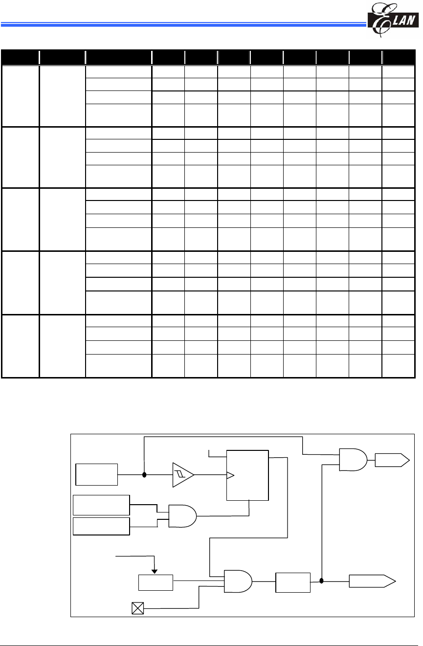
EM78P259N/260N
8-Bit Microprocessor with OTP ROM
40 • Product Specification (V1.2) 05.18.2007
(This specification is subject to change without further notice)
Address Name Reset Type Bit 7 Bit 6 Bit 5 Bit 4 Bit 3 Bit 2 Bit 1 Bit 0
Bit Name “0” “0” “0” “0” AD11 AD10 AD9 AD8
Power-on 0 0 0 0 U U U U
/RESET and WDT 0 0 0 0 U U U U
0XC RC
(ADDATA1H)
Wake-up from Pin
Change 0 0 0 0 P P P P
Bit Name AD7 AD6 AD5 AD4 AD3 AD2 AD1 AD0
Power-on U U U U U U U U
/RESET and WDT U U U U U U U U
0XD RD
(ADDATA1L0)
Wake-up from Pin
Change P P P P P P P P
Bit Name –- – ADIF CMPIF ADWE CMPWE ICWE –
Power-un 0 0 0 0 0 0 0 0
/RESET and WDT 0 0 0 0 0 0 0 0
0xE RE
(ISR2)
Wake-up from Pin
Change P P P P P P P P
Bit Name LPWTIF HPWTIF TCCCIF TCCBIF TCCAIF EXIF ICIF TCIF
Power-on 0 0 0 0 0 0 0 0
/RESET and WDT 0 0 0 0 0 0 0 0
0xF RF
(ISR1)
Wake-up from Pin
Change P P P P P P P P
Bit Name – – – – – – – –
Power-on U U U U U U U U
/RESET and WDT P P P P P P P P
0x10~0x3F R10~R3F
Wake-up from Pin
Change P P P P P P P P
Legend: ×: Not used U: Unknown or don’t care
P: Previous value before reset t: Check table under Section 6.5.2.
6.5.1.3 Controller Reset Block Diagram
WDT
Timeout
Oscillator
D Q
CLK
CLR
WDT
VDD
Setup
time
Reset
CLK
/RESET
Power-on Reset
Voltage
Detector
ENWDTB
Fig. 6-7 Controller Reset Block Diagram
EM78P259N/260N
8-Bit Microprocessor with OTP ROM
Product Specification (V1.2) 05.18.2007 • 41
(This specification is subject to change without further notice)
6.5.2 The T and P Status under STATUS (R3) Register
A reset condition is initiated by one of the following events:
1. Power-on reset
2. /RESET pin input "low"
3. WDT time-out (if enabled).
The values of RST, T, and P as listed in the table below, are used to check how the
processor wakes up.
Reset Type RST T P
Power-on 0 1 1
/RESET during Operating mode 0 *P *P
/RESET wake-up during Sleep mode 0 1 0
WDT during Operating mode 0 0 1
WDT wake-up during Sleep mode 0 0 0
Wake-up on pin change during Sleep mode 1 1 0
*P: Previous status before reset
The following shows the events that may affect the status of T and P.
Event RST T P
Power-on 0 1 1
WDTC instruction *P 1 1
WDT time-out 0 0 *P
SLEP instruction *P 1 0
Wake-up on pin changed during Sleep mode 1 1 0
*P: Previous value before reset
6.6 Interrupt
The EM78P259N/260N has six interrupts as listed below:
1. TCC, TCCA, TCCB, TCCC overflow interrupt
2. Port 5 Input Status Change Interrupt
3. External interrupt [(P60, /INT) pin]
4. Analog to Digital conversion completed
5. IR/PWM underflow interrupt
6. When the comparators status changes
Before the Port 5 Input Status Change Interrupt is enabled, reading Port 5 (e.g. "MOV
R5,R5") is necessary. Each Port 5 pin will have this feature if its status changes. The
Port 5 Input Status Change Interrupt will wake-up the EM78P259N/260N from the
sleep mode if it is enabled prior to going into the sleep mode by executing SLEP
instruction. When wake-up occurs, the controller will continue to execute program
in-line if the global interrupt is disabled. If enabled, the global interrupt will branch out to
the interrupt Vector 006H.

EM78P259N/260N
8-Bit Microprocessor with OTP ROM
42 • Product Specification (V1.2) 05.18.2007
(This specification is subject to change without further notice)
The external interrupt has an on-chip digital noise rejection circuit. Input pulse less
than 8 system clock time is eliminated as noise. However, in Low Crystal oscillator
(LXT) mode the noise rejection circuit is disabled. Edge selection is possible with INTE
of CONT. When an interrupt is generated by the External interrupt (when enabled), the
next instruction will be fetched from Address 003H. Refer to Word 1 Bits 9 & 8, Section
6.14.2, Code Option Register (Word 1) for digital noise rejection definition
RF and RE are the interrupt status register that records the interrupt requests in the
relative flags/bits. IOCF0 and IOCE0 are interrupt mask registers. The global interrupt
is enabled by the ENI instruction and is disabled by the DISI instruction. Once in the
interrupt service routine, the source of an interrupt can be determined by polling the flag
bits in RF. The interrupt flag bit must be cleared by instructions before leaving the
interrupt service routine to avoid recursive interrupts.
The flag (except for the ICIF bit) in the Interrupt Status Register (RF) is set regardless of
the ENI execution. Note that the result of RF will be the logic AND of RF and IOCF0
(refer to figure below). The RETI instruction ends the interrupt routine and enables the
global interrupt (the ENI execution).
When an interrupt is generated by the Timer clock/counter (if enabled), the next
instruction will be fetched from Address 009, 018, 01B, and 01EH (TCC, TCCA, TCCB,
and TCCC respectively).
When an interrupt generated by the AD conversion is completed (if enabled), the next
instruction will be fetched from Address 00CH.
When an interrupt is generated by the High time / Low time down counter underflow (if
enabled), the next instruction will be fetched from Address 012 and 015H (High time
and Low time respectively).
When an interrupt is generated by the Comparators (if enabled), the next instruction will
be fetched from Address 00FH (Comparator interrupt).
Before the interrupt subroutine is executed, the contents of ACC and the R3 and R4
registers will be saved by the hardware. If another interrupt occurs, the ACC, R3, and
R4 will be replaced by the new interrupt. After the interrupt service routine is completed,
the ACC, R3, and R4 registers are restored.
EM78P259N/260N
8-Bit Microprocessor with OTP ROM
Product Specification (V1.2) 05.18.2007 • 43
(This specification is subject to change without further notice)
INT
ENI/DISI
IOD
RFWR
IOCFRD
IOCFWR
IRQn
IRQm
RFRD
IOCF
/RESET
/IRQn
VCC
RF
CLK
CLK
Q
Q
D
P
R
L
C
_
P
R
L
C
Q
Q
_
D
Fig. 6-8 Interrupt Input Circuit
Interrupt sources
Interrupt
occurs
ENI/
DISI STACKACC
STACKR3
RETI
ACC
R3
R4 STACKR4
Fig. 6-9 Interrupt Backup Diagram
In EM78P259N/260N, each individual interrupt source has its own interrupt vector as
depicted in the table below.
Interrupt Vector Interrupt Status Priority *
003H External interrupt 1
006H Port 5 pin change 2
009H TCC overflow interrupt 3
00CH AD conversion complete interrupt 4
00FH Comparator interrupt 5
012H High-pulse width timer underflow interrupt 6
015H Low-pulse width timer underflow interrupt 7
018H TCCA overflow interrupt 8
01BH TCCB overflow interrupt 9
01EH TCCC overflow interrupt 10
*Priority: 1 = highest ; 10 = lowest priority
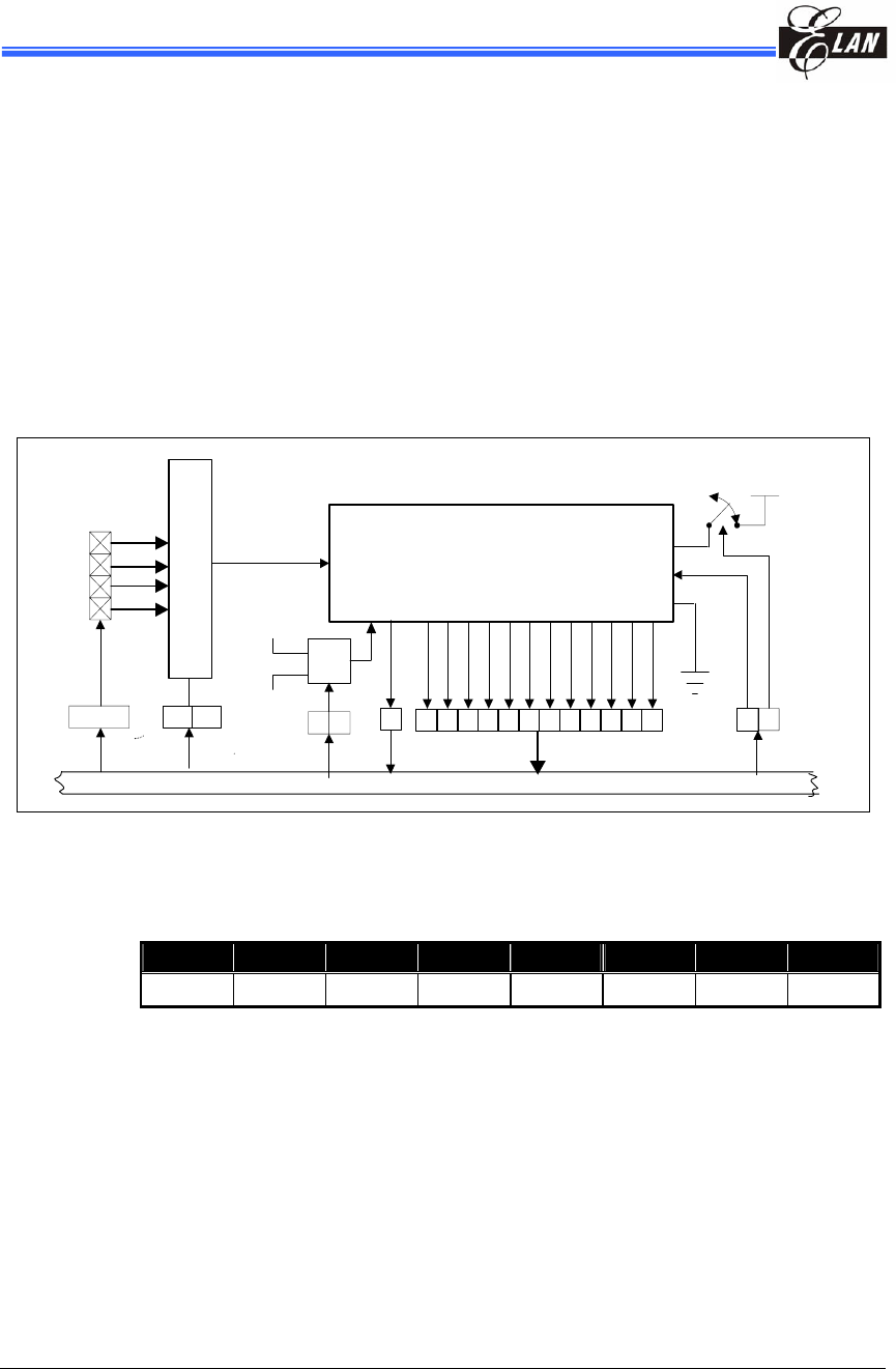
EM78P259N/260N
8-Bit Microprocessor with OTP ROM
44 • Product Specification (V1.2) 05.18.2007
(This specification is subject to change without further notice)
6.7 Analog-to-Digital Converter (ADC)
The analog-to-digital circuitry consist of a 4-bit analog multiplexer; three control
registers (AISR/R8, ADCON/R9, & ADOC/RA), three data registers (ADDATA/RB,
ADDATA1H/RC, & ADDATA1L/RD), and an ADC with 12-bit resolution as shown in the
functional block diagram below. The analog reference voltage (Vref) and the analog
ground are connected via separate input pins. Connecting to the external VREF is
more accurate than connecting to the internal VDD.
The ADC module utilizes successive approximation to convert the unknown analog
signal into a digital value. The result is fed to the ADDATA, ADDATA1H, and
ADDATA1L. Input channels are selected by the analog input multiplexer via the
ADCON register Bits ADIS1 and ADIS0.
ADDATA1H
DATA BUS
ADC3
ADC2
ADC1
ADC0
Vref
Power-Down
Fsco
Internal RC
4-1
MUX
7 ~ 0 34
ADC
( successive approximation )
3
56
ADCON RF
AISR ADCON
Start to Convert
01
ADCON
8-1 Analog Switch
01234567891011
ADDATA1L
Fig. 6-10 Analog-to-Digital Conversion Functional Block Diagram
6.7.1 ADC Control Register (AISR/R8, ADCON/R9, ADOC/RA)
6.7.1.1 R8 (AISR: ADC Input Select Register)
Bit 7 Bit 6 Bit 5 Bit 4 Bit 3 Bit 2 Bit 1 Bit 0
– – – – ADE3 ADE2 ADE1 ADE0
The AISR register individually defines the Port 5 pins as analog input or as digital I/O.
Bit 7 ~ 4: Not used
Bit 3 (ADE3): AD converter enable bit of P53 pin
0 = Disable ADC3, P53 acts as I/O pin
1 = Enable ADC3 acts as analog input pin
Bit 2 (ADE2): AD converter enable bit of P52 pin
0 = Disable ADC2, P53 acts as I/O pin
1 = Enable ADC2 acts as analog input pin
EM78P259N/260N
8-Bit Microprocessor with OTP ROM
Product Specification (V1.2) 05.18.2007 • 45
(This specification is subject to change without further notice)
Bit 1 (ADE1): AD converter enable bit of P51 pin
0 = Disable ADC1, P51 acts as I/O pin
1 = Enable ADC1 acts as analog input pin
Bit 0 (ADE0): AD converter enable bit of P50 pin
0 = Disable ADC0, P50 acts as I/O pin
1 = Enable ADC0 acts as analog input pin
6.7.1.2 R9 (ADCON: AD Control Register)
Bit 7 Bit 6 Bit 5 Bit 4 Bit 3 Bit 2 Bit 1 Bit 0
VREFS CKR1 CKR0 ADRUN ADPD - ADIS1 ADIS0
The ADCON register controls the operation of the AD conversion and determines
which pin should be currently active.
Bit 7(VREFS): Input source of the ADC Vref
0 = The ADC Vref is connected to Vdd (default value), and the
P54/VREF pin carries out the P54 function
1 = The ADC Vref is connected to P54/VREF
NOTE
The P54/TCC/VREF pin cannot be applied to TCC and VREF at the same time. IF
P54/TCC/VREF acts as VREF analog input pin, then CONT Bit 5 (TS) must be “0”.
The P54/TCC/VREF pin priority is as follows:
Bit 6 ~ Bit 5 (CKR1 ~ CKR0): The ADC prescaler oscillator clock rate
00 = 1: 16 (default value)
01 = 1: 4
10 = 1: 64
11 = 1: WDT ring oscillator frequency
CKR1:CKR0 Operation Mode Max. Operation Frequency
00 Fosc/16 4 MHz
01 Fosc/4 1 MHz
10 Fosc/64 16 MHz
11 Internal RC –
P54/TCC/VREF Pin Priority
High Medium Low
VREF TCC P54

EM78P259N/260N
8-Bit Microprocessor with OTP ROM
46 • Product Specification (V1.2) 05.18.2007
(This specification is subject to change without further notice)
Bit 4 (ADRUN): ADC starts to RUN.
0 = reset on completion of the conversion. This bit cannot be reset
though software.
1 = an AD conversion is started. This bit can be set by software.
Bit 3 (ADPD): ADC Power-down mode.
0 = switch off the resistor reference to save power even
while the CPU is operating.
1 = ADC is operating
Bit 2: Not used
Bit 1 ~ Bit 0 (ADIS1 ~ ADIS0): Analog Input Select
00 = ADIN0/P50
01 = ADIN1/P51
10 = ADIN2/P52
11 = ADIN3/P53
These bits can only be changed when the ADIF bit and the ADRUN bit
are both LOW.
6.7.1.3 RA (ADOC: AD Offset Calibration Register)
Bit 7 Bit 6 Bit 5 Bit 4 Bit 3 Bit 2 Bit 1 Bit 0
CALI SIGN VOF[2] VOF[1] VOF[0] – – –
Bit 7 (CALI): Calibration enable bit for ADC offset
0 = Calibration disable
1 = Calibration enable
Bit 6 (SIGN): Polarity bit of offset voltage
0 = Negative voltage
1 = Positive voltage
Bit 5 ~ Bit 3 (VOF[2] ~ VOF[0]): Offset voltage bits.
VOF[2] VOF[1] VOF[0] EM78P259N/260N ICE259N
0 0 0 0LSB 0LSB
0 0 1 2LSB 1LSB
0 1 0 4LSB 2LSB
0 1 1 6LSB 3LSB
1 0 0 8LSB 4LSB
1 0 1 10LSB 5LSB
1 1 0 12LSB 6LSB
1 1 1 14LSB 7LSB
Bit 2 ~ Bit 0: Unimplemented, read as ‘0’.

EM78P259N/260N
8-Bit Microprocessor with OTP ROM
Product Specification (V1.2) 05.18.2007 • 47
(This specification is subject to change without further notice)
6.7.2 ADC Data Register (ADDATA/RB, ADDATA1H/RC,
ADDATA1L/RD)
When the AD conversion is completed, the result is loaded to the ADDATA, ADDATA1H
and ADDATA1L registers. The ADRUN bit is cleared, and the ADIF is set.
6.7.3 ADC Sampling Time
The accuracy, linearity, and speed of the successive approximation of AD converter are
dependent on the properties of the ADC and the comparator. The source impedance
and the internal sampling impedance directly affect the time required to charge the
sample holding capacitor. The application program controls the length of the sample
time to meet the specified accuracy. Generally speaking, the program should wait for
2μs for each KΩ of the analog source impedance and at least 2μs for the
low-impedance source. The maximum recommended impedance for analog source is
10KΩ at Vdd=5V. After the analog input channel is selected, this acquisition time must
be done before the conversion is started.
6.7.4 AD Conversion Time
CKR1 and CKR0 select the conversion time (Tct), in terms of instruction cycles. This
allows the MCU to run at a maximum frequency without sacrificing the AD conversion
accuracy. For the EM78P259N/260N, the conversion time per bit is about 4μs. The
table below shows the relationship between Tct and the maximum operating
frequencies.
CKR1:CKR0 Operation
Mode Max. Operation
Frequency Max. Conversion
Rate/Bit Max. Conversion Rate
00 Fosc/16 4 MHz 250kHz (4μs) 15*4μs=60μs (16.7kHz)
01 Fosc/4 1 MHz 250kHz (4μs) 15*4μs=60μs (16.7kHz)
10 Fosc/64 16 MHz 250kHz ( 4μs) 15*4μs=60μs (16.7kHz)
11 Internal RC – 14kHz (71μs) 15*71μs=1065μs (0.938kHz)
NOTE
■ Pin not used as an analog input pin can be used as a regular input or output pin.
■ During conversion, do not perform output instruction to maintain precision for all of
the pins.
6.7.5 ADC Operation during Sleep Mode
In order to obtain a more accurate ADC value and reduce power consumption, the AD
conversion remains operational during sleep mode. As the SLEP instruction is
executed, all the MCU operations will stop except for the Oscillators TCC, TCCA,
TCCB, TCCC and AD conversion.
The AD Conversion is considered completed as determined by:
1. ADRUN bit of R9 register is cleared (“0” value).
2. ADIF bit of RE register is set to “1”.

EM78P259N/260N
8-Bit Microprocessor with OTP ROM
48 • Product Specification (V1.2) 05.18.2007
(This specification is subject to change without further notice)
3. ADWE bit of the RE register is set to “1.” Wake-up from ADC conversion (where it
remains in operation during sleep mode).
4. Wake-up and executes the next instruction if ADIE bit of IOCE0 is enabled and the
“DISI” instruction is executed.
5. Wake-up and enters into Interrupt vector (Address 0x00C) if ADIE bit of IOCE0 is
enabled and the “ENI” instruction is executed.
6. Enters into Interrupt vector (Address 0x00C) if ADIE bit of IOCE0 is enabled and the
“ENI” instruction is executed.
The results are fed into the ADDATA, ADDATA1H, and ADDATA1L registers when the
conversion is completed. If the ADIE is enabled, the device will wake up. Otherwise,
the AD conversion will be shut off, no matter what the status of ADPD bit is.
6.7.6 Programming Process/Considerations
6.7.6.1 Programming Process
Follow these steps to obtain data from the ADC:
1. Write to the four bits (ADE3:ADE0) on the R8 (AISR) register to define the
characteristics of R5 (digital I/O, analog channels, or voltage reference pin)
2. Write to the R9/ADCON register to configure the AD module:
a) Select the ADC input channel (ADIS1:ADIS0)
b) Define the AD conversion clock rate (CKR1:CKR0)
c) Select the VREFS input source of the ADC
d) Set the ADPD bit to 1 to begin sampling
3. Set the ADWE bit, if the wake-up function is employed
4. Set the ADIE bit, if the interrupt function is employed
5. Write “ENI” instruction, if the interrupt function is employed
6. Set the ADRUN bit to 1
7. Write “SLEP” instruction or Polling.
8. Wait for wake-up, ADRUN bit is cleared (“0” value), interrupt flag (ADIF) to be set
“1,” or the ADC interrupt to occur.
9. Read the ADDATA or ADDATA1H and ADDATA1L conversion data registers. If the
ADC input channel changes at this time, the ADDATA, ADDATA1H, and
ADDATA1L values can be cleared to ‘0’.
10. Clear the interrupt flag bit (ADIF)
11. For the next conversion, go to Step 1 or Step 2 as required. At least 2 Tct is
required before the next acquisition starts.

EM78P259N/260N
8-Bit Microprocessor with OTP ROM
Product Specification (V1.2) 05.18.2007 • 49
(This specification is subject to change without further notice)
NOTE
In order to obtain accurate values, it is necessary to avoid any data transition on the
I/O pins during AD conversion.
6.7.6.2 Sample Demo Programs
A. Define a General Register
R_0 == 0 ; Indirect addressing register
PSW == 3 ; Status register
PORT5 == 5
PORT6 == 6
R_E== 0XE ; Interrupt status register
B. Define a Control Register
IOC50 == 0X5 ; Control Register of Port 5
IOC60 == 0X6 ; Control Register of Port 6
C_INT== 0XF ; Interrupt Control Register
C. ADC Control Register
ADDATA == 0xB ; The contents are the results of ADC
AISR == 0x08 ; ADC input select register
ADCON == 0x9 ; 7 6 5 4 3 2 1 0
; VREFS CKR1 CKR0 ADRUN ADPD ADIS2 ADIS1 ADIS0
D. Define Bits in ADCON
ADRUN == 0x4 ; ADC is executed as the bit is set
ADPD == 0x3 ; Power Mode of ADC
E. Program Starts
ORG 0 ; Initial address
JMP INITIAL ;
ORG 0x0C ; Interrupt vector
JMP CLRRE
;
;
;(User program section)
;
;
CLRRE:
MOV A,RE
AND A, @0BXX0XXXXX ; To clear the ADIF bit, “X” by application
MOV RE,A
BS ADCON, ADRUN ; To start to execute the next AD conversion
if necessary

EM78P259N/260N
8-Bit Microprocessor with OTP ROM
50 • Product Specification (V1.2) 05.18.2007
(This specification is subject to change without further notice)
RETI
INITIAL:
MOV A,@0B00000001 ; To define P50 as an analog input
MOV AISR,A
MOV A,@0B00001000 ; To select P50 as an analog input channel, and
AD power on
MOV ADCON,A ; To define P50 as an input pin and set clock
rate at fosc/16
En_ADC:
MOV A, @0BXXXXXXX1 ; To define P50 as an input pin, and the others
IOW PORT5 ; are dependent on applications
MOV A, @0BXXXX1XXX ; Enable the ADWE wake-up function of ADC, “X”
by application
MOV RE,A
MOV A, @0BXXXX1XXX ; Enable the ADIE interrupt function of ADC,
“X” by application
IOW C_INT
ENI ; Enable the interrupt function
BS ADCON, ADRUN ; Start to run the ADC
; If the interrupt function is employed, the following three lines
may be ignored
;If Sleep:
SLEP
;
;(User program section)
;
or
;If Polling:
POLLING:
JBC ADCON, ADRUN ; To check the ADRUN bit continuously;
JMP POLLING ; ADRUN bit will be reset as the AD conversion
is completed
;
;(User program section)
;
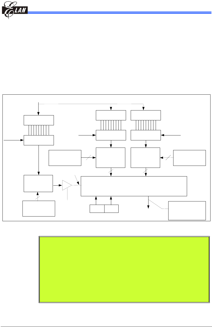
EM78P259N/260N
8-Bit Microprocessor with OTP ROM
Product Specification (V1.2) 05.18.2007 • 51
(This specification is subject to change without further notice)
6.8 Infrared Remote Control Application/PWM Waveform
Generation
6.8.1 Overview
This LSI can easily output infrared carrier or PWM standard waveform. As illustrated
below, the IR and PWM waveform generation function include an 8-bit down count
timer/counter, high time, low time, and IR control register. The IROUT pin waveform is
determined by IOCA0 (IR and TCCC scale control register), IOCB1 (high time rate, low
time rate control register), IOC81 (TCCC counter), IOCA1 (high time register), and
IOC91 (low time register).
H/W Modulator
8
HF
IROUT
pin
IRE
Fcarrier
FT:CLK(Fosc)
LGP
8 Bit counter
8-to-1 MUX
8bit binary
down counter
Auto-reload buffer
(TCCC)(IOC81)
8 Bit counter
8-to-1 MUX
8 Bit counter
8-to-1 MUX
8bit binary
down counter
8bit binary
down counter
Auto-reload buffer
(High-time)(IOCA1)
Auto-reload buffer
(Low-time)(IOC91)
88
Scale
(IOCB1)
Scale
(IOCB1)
Scale
(IOCA0)
88
Underflow Interrupt
HPWTIF
LPWTIF
Fig. 6-11 IR/PWM System Block Diagram
NOTE
Details of the Fcarrier high time width and low time width are explained below:
Fcarrier = FT/ 2 { [1+decimal TCCC Counter value (IOC81)] * TCCC
Scale (IOCA0) }
High time width = { [1+decimal high time value (IOCA1)] * High time Scale
(IOCB1) } / FT
Low time width = { [1+decimal low time value (IOC91)] * Low time Scale
(IOCB1) } / FT
Where FT is the system clock FT=Fosc/1 (CLK=2)
FT=Fosc/2 (CLK=4)
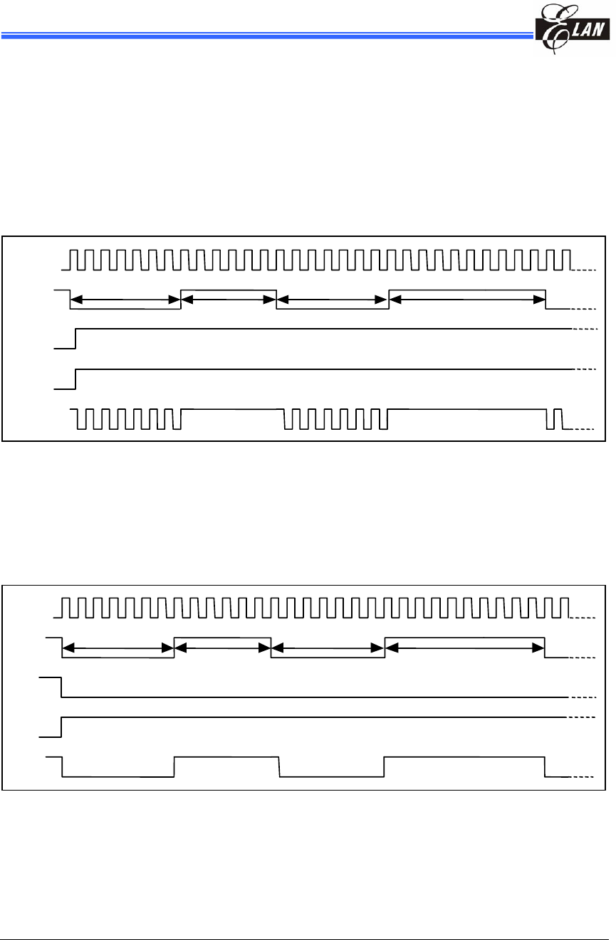
EM78P259N/260N
8-Bit Microprocessor with OTP ROM
52 • Product Specification (V1.2) 05.18.2007
(This specification is subject to change without further notice)
When an interrupt is generated by the High time down counter underflow (if enabled),
the next instruction will be fetched from Address 018 and 01BH (High time and Low
time, respectively).
6.8.2 Function Description
The following figure shows LGP=0 and HF=1. The IROUT waveform modulates the
Fcarrier waveform at low time segments of the pulse.
Fig. 6-12a LGP=0, HF=1, IROUT Pin Output Waveform
The following figure shows LGP=0 and HF=0. The IROUT waveform cannot modulate
the Fcarrier waveform at low time segments of the pulse. So IROUT waveform is
determined by the high time width and low time width instead. This mode can produce
standard PWM waveform
Fig. 6-12b LGP=0, HF=0, IROUT Pin Output Waveform
Fcarrier
IROUT
HF
IRE
high time widthlow time width high time width low time width
start
Fcarrier
IROUT
start
HF
IRE
high time widthlow time width high time width low time width
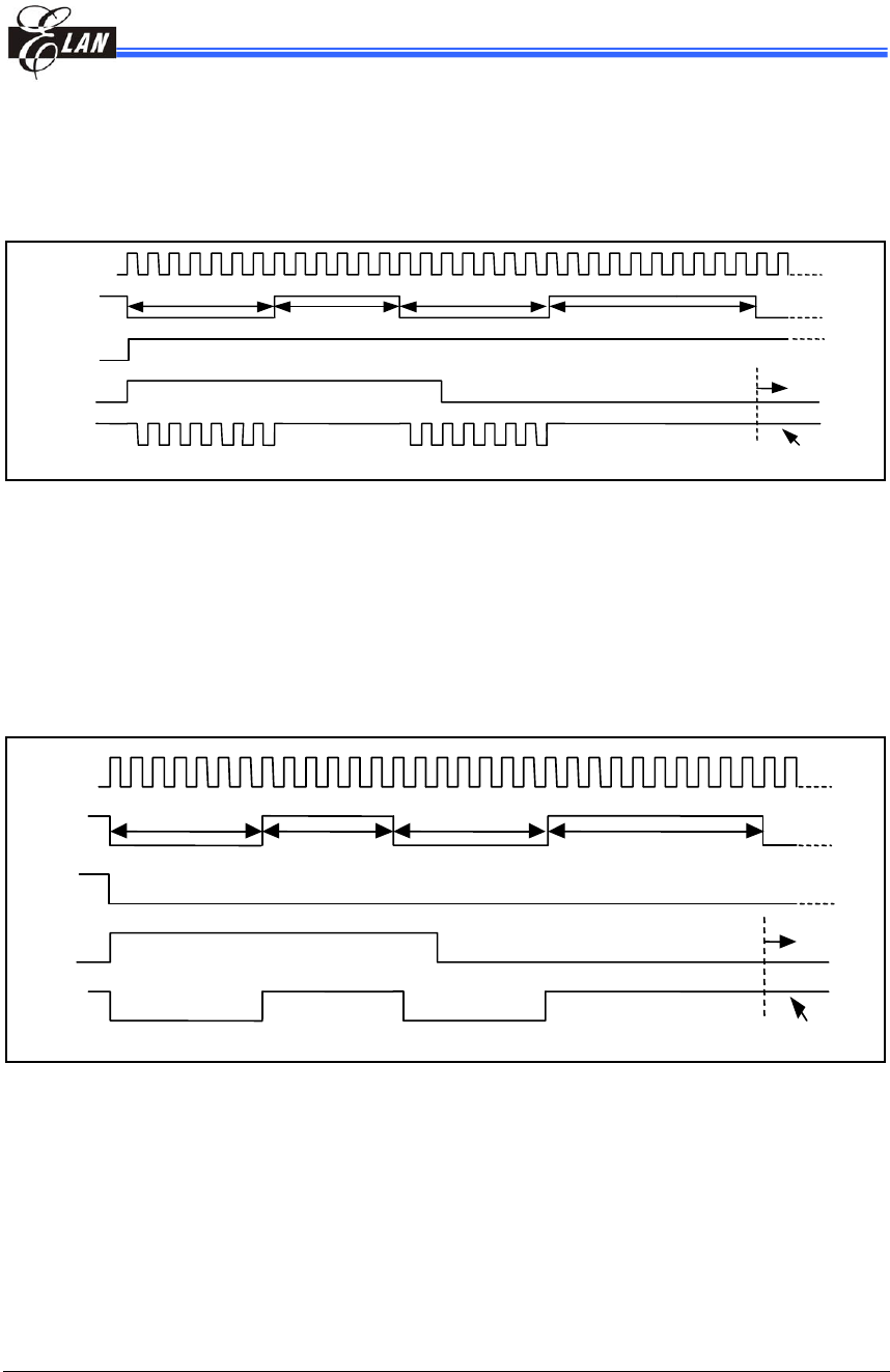
EM78P259N/260N
8-Bit Microprocessor with OTP ROM
Product Specification (V1.2) 05.18.2007 • 53
(This specification is subject to change without further notice)
The following figure shows LGP=0 and HF=1. The IROUT waveform modulates the
Fcarrier waveform at low time segments of the pulse. When IRE goes low from high,
the output waveform of IROUT will keep transmitting untill high time interrupt occurs.
Fig. 6-12c LGP=0, HF=1, When IRE goes Low from High, IROUT Pin Outputs Waveform
The following figure shows LGP=0 and HF=0. The IROUT waveform cannot modulate
the Fcarrier waveform at low time segments of the pulse. So IROUT waveform is
determined by high time width and low time width. This mode can produce standard
PWM waveform when IRE goes low from high. The output waveform of IROUT will
keep on transmitting till high time interrupt occurs.
Fig. 6-12d LGP=0, HF=0, When IRE goes Low from High, Irout Pin Output Waveform
Fcarrier
IROUT
HF
IRE IR disable
Always high-level
start
high time widthlow time width high time width low time width
Fcarrier
IROUT
HF
IRE IR disable
Always high- level
star
t
hi
g
h time widthlow time width hi
g
h time widthlow time width
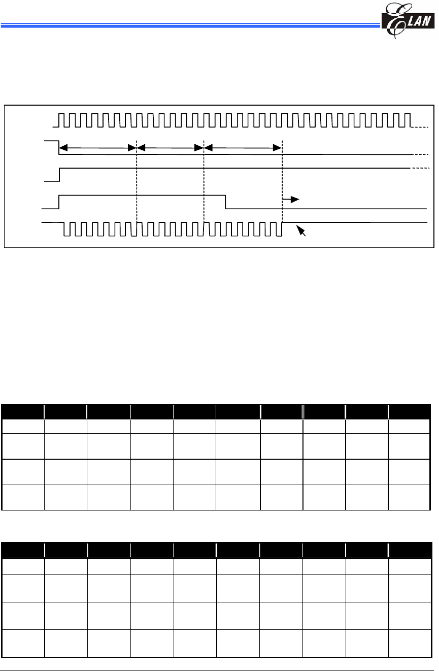
EM78P259N/260N
8-Bit Microprocessor with OTP ROM
54 • Product Specification (V1.2) 05.18.2007
(This specification is subject to change without further notice)
The following figure shows LGP=1 and HF=1. When this bit is set to high level, the high
time segment of the pulse is ignored. So, IROUT waveform output is determined by
low time width.
Fig. 6-12e LGP=1 and HF=1, IROUT Pin Output Waveform
6.8.3 Programming the Related Registers
When defining IR/PWM, refer to the operation of the related registers as shown in the
tables below.
IR/PWM Related Control Registers
Address Name Bit 7 Bit 6 Bit 5 Bit 4 Bit 3 Bit 2 Bit 1 Bit 0
0x09 IOC90 TCCBHE/0 TCCBEN/0 TCCBTS/0 TCCBTE/0 0 TCCCEN/0 TCCCTS/0 TCCCTE/0
0X0A IR CR
/IOCA0 TCCCSE/0 TCCCS2/0 TCCCS1/0 TCCCS0/0 IRE/0 HF/0 LGP/0 IROUTE/0
0x0F IMR
/IOCF0 LPWTIE/0 HPWTIE/0 TCCCIE/0 TCCBIE/0 TCCAIE/0 EXIE/0 ICIE/0 TCIE/0
0X0B HLTS
/IOCB1 HTSE/0 HTS2/0 HTS1/0 HTS0/0 LTSE/0 LTS2/0 LTS1/0 LTS0/0
IR/PWM Related Status/Data Registers
Address Name Bit 7 Bit 6 Bit 5 Bit 4 Bit 3 Bit 2 Bit 1 Bit 0
0x0F ISR/RF LPWTIF/0 HPWTIF/0 TCCCIF/0 TCCBIF/0 TCCAIF/0 EXIF/0 ICIF/0 TCIF/0
0x06 TCCC
/IOC81 TCCC7/0 TCCC6/0 TCCC5/0 TCCC4/0 TCCC3/0 TCCC2/0 TCCC1/0 TCCC0/0
0X09 LTR
/IOC91 LTR7/0 LTR6/0 LTR5/0 LTR4/0 LTR3/0 LTR2/0 LTR1/0 LTR0/0
0X0A HTR
/IOCA1 HTR7/0 HTR6/0 HTR5/0 HTR4/0 HTR3/0 HTR2/0 HTR1/0 HTR0/0
Fcarrier
IROUT
HF
IRE IR disable
Always high-level
start
low time widthlow time width high time width low time width

EM78P259N/260N
8-Bit Microprocessor with OTP ROM
Product Specification (V1.2) 05.18.2007 • 55
(This specification is subject to change without further notice)
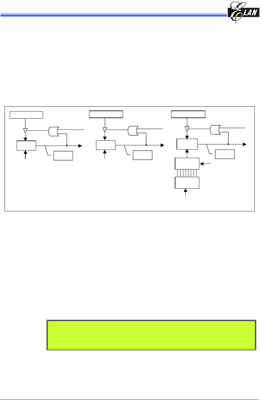
EM78P259N/260N
8-Bit Microprocessor with OTP ROM
56 • Product Specification (V1.2) 05.18.2007
(This specification is subject to change without further notice)
6.9 Timer/Counter
6.9.1 Overview
Timer A (TCCA) is an 8-bit clock counter. Timer B (TCCB) is a 16-bit clock counter.
Timer C (TCCC) is an 8-bit clock counter that can be extended to 16-bit clock counter
with programmable scalers. TCCA, TCCB, and TCCC can be read and written to, and
are cleared at every reset condition.
6.9.2 Function Description
Set predict value
System clock or
External input External input
TCCC
Set TCCCIF
TCCCEN
Overflow
TCCA
Set TCCAIF
TCCAEN
Overflow
TCCB
Set TCCBIF
TCCBEN
Overflow
Set predict value Set predict value
External input
8-to-1 MUX
8 Bit
counter
System clock or
System clock or
TCCCS1 ~ TCCCS0
Fig. 6-13 Timer Block Diagram
Each signal and block of the above TIMER block diagram is described as follows:
TCCX: Timer A~C register. TCCX increases until it matches with zero, and then
reloads the predicted value. When writing a value to TCCX, the predicted
value and TCCX value become the set value. When reading from TCCX, the
value will be the TCCX direct value. When TCCXEN is enabled, the reload of
the predicted value to TCCX, TCCXIE is also enabled. TCCXIF will be set at
the same time. It is an Up Counter.
Under TCCA Counter (IOC51):
IOC51 (TCCA) is an 8-bit clock counter. It can be read, written to, and cleared
on any reset condition and is an Up Counter.
NOTE
■ TCCA time-out period [1/Fosc x (256-TCCA cnt) x 1 (CLK=2)]
■ TCCA time-out period [1/Fosc x (256-TCCA cnt) x 2 (CLK=4)]
Under TCCB Counter (IOC61):
TCCB (IOC61) is an 8-bit clock counter for the least significant byte of TCCBX
(TCCB). It can be read, written to, and cleared on any reset condition and is an
Up Counter.

EM78P259N/260N
8-Bit Microprocessor with OTP ROM
Product Specification (V1.2) 05.18.2007 • 57
(This specification is subject to change without further notice)
Under TCCBH / MSB Counter (IOC71):
TCCBH/MSB (IOC71) is an 8-bit clock counter is for the most significant byte of
TCCBX (TCCBH). It can be read, written to, and cleared on any reset
condition.
When TCCBHE (IOC90) is “0,” then TCCBH is disabled. When TCCBHE is”1,”
then TCCB is a 16-bit length counter.
NOTE
When TCCBH is Disabled:
TCCB time-out period [1/Fosc x ( 256 - TCCB cnt ) x 1(CLK=2)]
TCCB time-out period [1/Fosc x ( 256 - TCCB cnt ) x 2(CLK=4)]
When TCCBH is Enabled:
TCCB time-out period {1/Fosc x [ 65536 - (TCCBH * 256 + TCCB cnt)] x 1(CLK=2)}
TCCB time-out period {1/Fosc x [ 65536 - (TCCBH * 256 + TCCB cnt)] x 2(CLK=4)}
Under TCCC Counter (IOC81):
IOC81 (TCCC) is an 8-bit clock counter. It can be read, written, and cleared on
any reset condition.
If HF (Bit 2 of IOCA0) = 1 and IRE (Bit 3 of IOCA0) = 1, TCCC counter scale
uses the low time segments of the pulse generated by Fcarrier frequency
modulation (see Fig. 6-12 in Section 6.8.2, Function Description). Then the
TCCC value will be the TCCC predicted value.
When HF = 0 or IRE = 0, the TCCC is an Up Counter.
NOTE
In TCCC Up Counter mode:
■ TCCC timeout period [1/Fosc x scaler (IOCA0) x (256-TCCC cnt) x 1(CLK=2)]
■ TCCC timeout period [1/Fosc x scaler (IOCA0) x (256-TCCC cnt) x 2(CLK=4)]
When HF = 1 and IRE = 1, the TCCC counter scale uses the low time
segments of the pulse generated by Fcarrier frequency modulation.
NOTE
In IR mode:
■ Fcarrier = FT/ 2 { [1+decimal TCCC Counter value (IOC81)] * TCCC Scale (IOCA0) }
■ FT is system clock: FT = Fosc/1 (CLK=2)
FT = Fosc/2 (CLK=4)
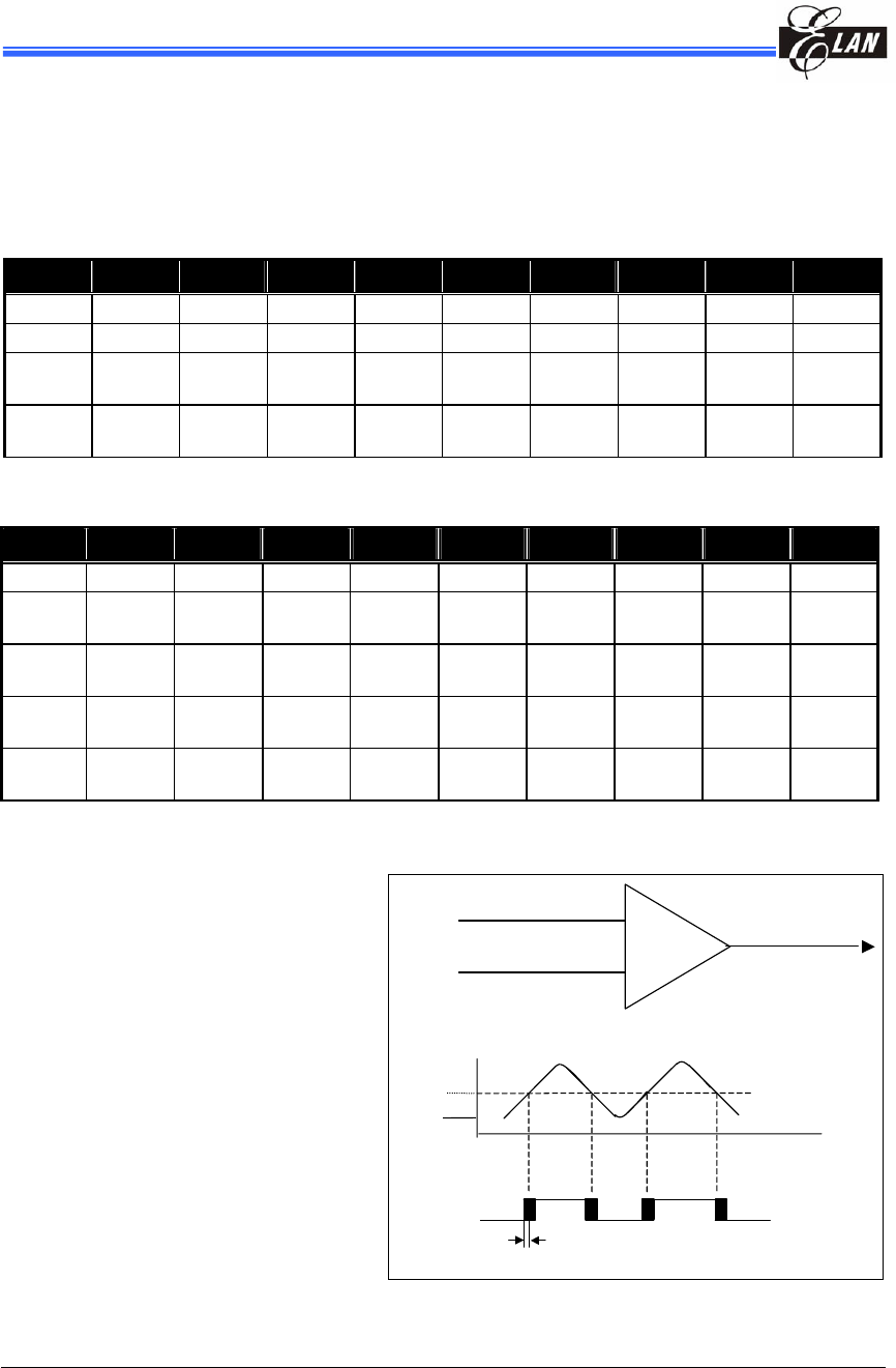
EM78P259N/260N
8-Bit Microprocessor with OTP ROM
58 • Product Specification (V1.2) 05.18.2007
(This specification is subject to change without further notice)
6.9.3 Programming the Related Registers
When defining TCCX, refer to its related registers operation as shown in the tables
below.
TCCX Related Control Registers:
Address Name Bit 7 Bit 6 Bit 5 Bit 4 Bit 3 Bit 2 Bit 1 Bit 0
0x08 IOC80 0 0 CPOUT/0 COS1/0 COS0/0 TCCAEN/0 TCCATS/0 TCCATE/0
0x09 IOC90 TCCBHE/0 TCCBEN/0 TCCBTS/0 TCCBTE/0 0 TCCCEN/0 TCCCTS/0 TCCCTE/0
0x0A IR CR
/IOCA0 TCCCSE/0 TCCCS2/0 TCCCS1/0 TCCCS0/0 IRE/0 HF/0 LGP/0 IROUTE/0
0x0F IMR
/IOCF0 LPWTE/0 HPWTE/0 TCCCIE/0 TCCBIE/0 TCCAIE/0 EXIE/0 ICIE/0 TCIE/0
Related TCCX Status/Data Registers:
Address Name Bit 7 Bit 6 Bit 5 Bit 4 Bit 3 Bit 2 Bit 1 Bit 0
0x0F ISR/RF LPWTF/0 HPWTF/0 TCCCIF/0 TCCBIF/0 TCCAIF/0 EXIF/0 ICIF/0 TCIF/0
0x05 TCCA
/IOC51 TCCA7/0 TCCA6/0 TCCA5/0 TCCA4/0 TCCA3/0 TCCA2/0 TCCA1/0 TCCA0/0
0x06 TCCB
/IOC61 TCCB7/0 TCCB6/0 TCCB5/0 TCCB4/0 TCCB3/0 TCCB2/0 TCCB1/0 TCCB0/0
0x07 TCCBH
/IOC71 TCCBH7/0 TCCBH6/0 TCCBH5/0 TCCBH4/0 TCCBH3/0 TCCBH2/0 TCCBH1/0 TCCBH0/0
0x08 TCCC
/IOC81 TCCC7/0 TCCC6/0 TCCC5/0 TCCC4/0 TCCC3/0 TCCC2/0 TCCC1/0 TCCC0/0
6.10 Comparator
EM78P259N/260N has
one comparator which
has two analog inputs and
one output. The
comparator can be
employed to wake-up
from the sleep mode.
Figure below shows the
circuit of the comparator.
Cin--
+
CMP
Cin+
CO
Cin+
Cin-
Output
30mV
Fig. 6-14 Comparator Operating Mode
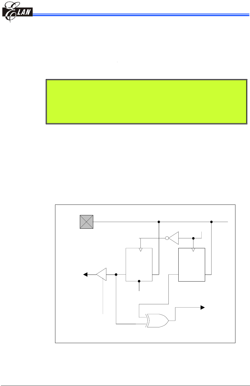
EM78P259N/260N
8-Bit Microprocessor with OTP ROM
Product Specification (V1.2) 05.18.2007 • 59
(This specification is subject to change without further notice)
6.10.1 External Reference Signal
The analog signal that is presented at Cin– compares to the signal at Cin+. The digital
output (CO) of the comparator is adjusted accordingly by taking the following notes into
considerations:
NOTE
■ The reference signal must be between Vss and Vdd.
■ The reference voltage can be applied to either pin of the comparator.
■ Threshold detector applications may be of the same reference.
■ The comparator can operate from the same or different reference sources.
6.10.2 Comparator Output
The compared result is stored in the CMPOUT of IOC80.
The comparator outputs are sent to CO (P64) through programming Bit 4 &
Bit 3<COS1, COS0> of the IOC80 register to <1,0>. See table under Section 6.2.4,
IOC80 (Comparator and TCCA Control Registers) for Comparator/OP select bits
function description.
The following figure shows the Comparator Output block diagram.
QQ
ENEN
D
D
To C0
To CPIF
To CMPOUT
CMRD
CMRD
From other
comparator
RESET
From OP I/O
Fig. 6-15 Comparator Output Configuration

EM78P259N/260N
8-Bit Microprocessor with OTP ROM
60 • Product Specification (V1.2) 05.18.2007
(This specification is subject to change without further notice)
6.10.3 Using a Comparator as an Operation Amplifier
The comparator can be used as an operation amplifier if a feedback resistor is
externally connected from the input to the output. In this case, the Schmitt trigger can
be disabled for power saving purposes, by setting Bit 4, Bit 3<COS1, COS0> of the
IOC80 register to <1,1>. See table under Section 6.2.4, IOC80 (Comparator and TCCA
Control Registers) for Comparator/OP select bits function description.
NOTE
Under Operation Amplifier:
■ The CMPIE (IOCE0.4), CMPWE (RE.2), and CMPIF (RE.4) bits are invalid.
■ The comparator interrupt is invalid.
■ The comparator wake-up is invalid.
6.10.4 Comparator Interrupt
CMPIE (IOCE0.4) must be enabled for the “ENI” instruction to take effect
Interrupt is triggered whenever a change occurs on the comparator output pin
The actual change on the pin can be determined by reading the Bit CMPOUT,
IOC80<5>.
CMPIF (RE.4), the comparator interrupt flag, can only be cleared by software
6.10.5 Wake-up from Sleep Mode
If the CMPWE bit of the RE register is set to “1,” the comparator remains active and
the interrupt remains functional, even under Sleep mode.
If a mismatch occurs, the change will wake up the device from Sleep mode.
The power consumption should be taken into consideration for the benefit of energy
conservation.
If the function is unemployed during Sleep mode, turn off the comparator before
entering into sleep mode.
The Comparator is considered completed as determined by:
1. COS1 and COS0 bits of IOC80 register setting selects Comparator.
2. CMPIF bit of RE register is set to “1”.
3. CMPWE bit of RE register is set to “1”. Wakes-up from Comparator (where it
remains in operation during sleep mode)
4. Wakes-up and executes the next instruction, if CMPIE bit of IOCE0 is enabled and
the “DISI” instruction is executed.
5. Wake-up and enters into Interrupt vector (address 0x00F), if ADIE bit of IOCE0 is
enabled and the “ENI” instruction is executed
6. Enters into Interrupt vector (address 0x00F), if CMPIE bit of IOCE0 is enabled and
the “ENI” instruction is executed.
EM78P259N/260N
8-Bit Microprocessor with OTP ROM
Product Specification (V1.2) 05.18.2007 • 61
(This specification is subject to change without further notice)
6.11 Oscillator
6.11.1 Oscillator Modes
The EM78P259N/260N can be operated in four different oscillator modes, such as High
Crystal oscillator mode (HXT), Low Crystal oscillator mode (LXT), External RC
oscillator mode (ERC), and RC oscillator mode with Internal RC oscillator mode (IRC).
You can select one of them by programming the OSC2, OCS1, and OSC0 in the Code
Option register.
The Oscillator modes defined by OSC2, OCS1, and OSC0 are described below.
Oscillator Modes OSC2 OSC1 OSC0
ERC1 (External RC oscillator mode); P70/OSCO acts as P70 0 0 0
ERC1 (External RC oscillator mode); P70/OSCO acts as OSCO 0 0 1
IRC2 (Internal RC oscillator mode); P70/OSCO acts as P70 0 1 0
IRC2 (Internal RC oscillator mode); P70/OSCO acts as OSCO 0 1 1
LXT3 (Low Crystal oscillator mode) 1 1 0
HXT3 High Crystal oscillator mode) (default) 1 1 1
1 In ERC mode, OSCI is used as oscillator pin. OSCO/P70 is defined by code option Word 0 Bit 6 ~ Bit 4.
2 In IRC mode, P55 is normal I/O pin. OSCO/P70 is defined by code option Word 0 Bit 6 ~ Bit 4.
3 In LXT and HXT modes; OSCI and OSCO are used as oscillator pins. These pins cannot and should not
be defined as normal I/O pins.
NOTE
The transient point of the system frequency between HXT and LXY is around 400kHz.
The maximum operating frequency limit of crystal/resonator at different VDDs, are as
follows:
Conditions VDD Max. Freq. (MHz)
2.3 4
3.0 8
Two clocks
5.0 20
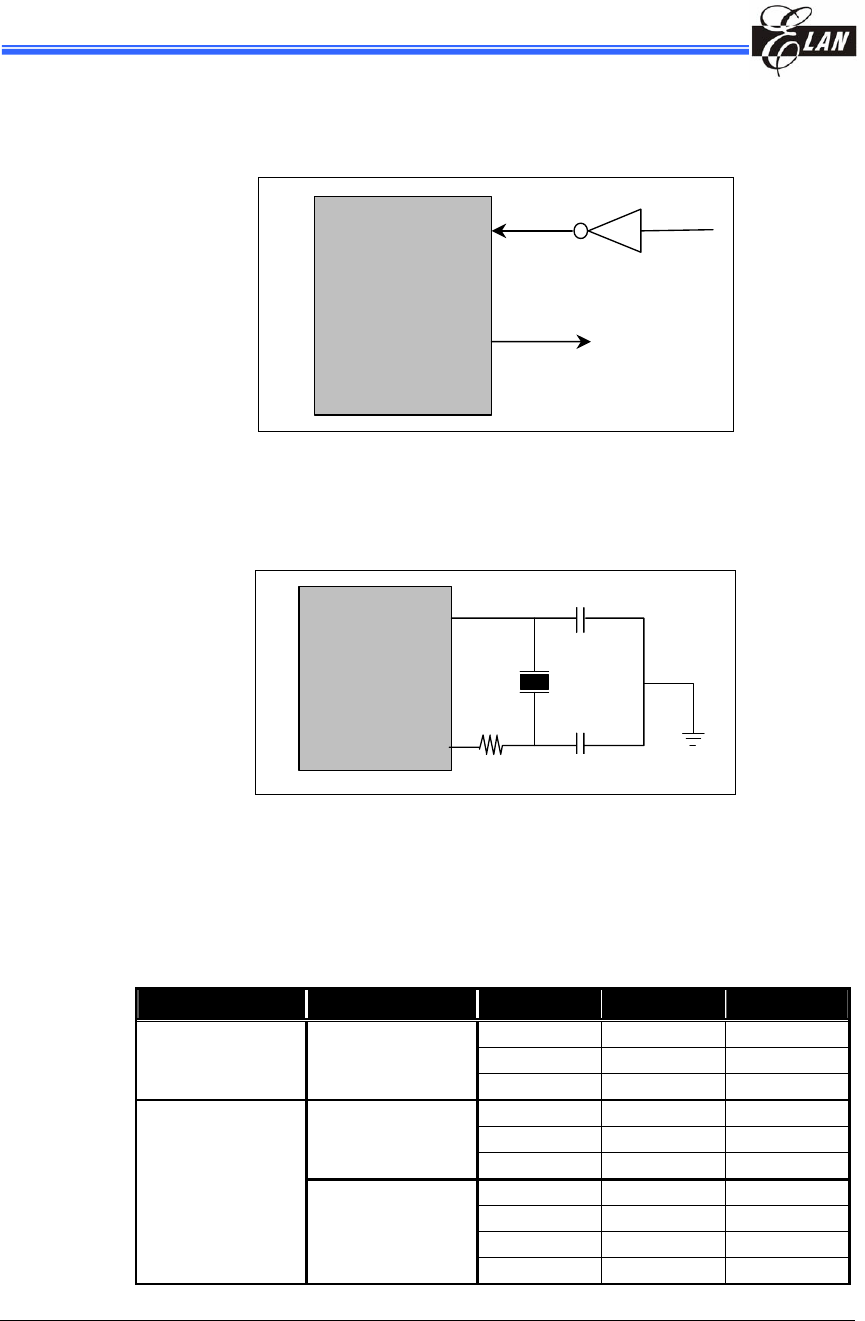
EM78P259N/260N
8-Bit Microprocessor with OTP ROM
62 • Product Specification (V1.2) 05.18.2007
(This specification is subject to change without further notice)
6.11.2 Crystal Oscillator/Ceramic Resonators (Crystal)
The EM78P259N/260N can be driven by an external clock signal through the OSCI pin
as illustrated below.
OSCI
OSCO
EM78P259N
EM78P260N
Fig. 6-16 External Clock Input Circuit
In most applications, Pin OSCI and Pin OSCO can be connected with a crystal or
ceramic resonator to generate oscillation. Fig. 6-17 below depicts such a circuit. The
same applies to the HXT mode and the LXT mode.
OSCI
EM78P259N
EM78P260N
OSCO
Crystal
RS C2
C1
Fig. 6-17 Crystal/Resonator Circuit
The following table provides the recommended values for C1 and C2. Since each
resonator has its own attribute, you should refer to the resonator specifications for the
appropriate values of C1 and C2. RS, a serial resistor, may be required for AT strip cut
crystal or low frequency mode.
Capacitor selection guide for crystal oscillator or ceramic resonators:
Oscillator Type Frequency Mode Frequency C1(pF) C2(pF)
455kHz 100~150 100~150
2.0 MHz 20~40 20~40
Ceramic Resonators HXT
4.0 MHz 10~30 10~30
32.768kHz 25 15
100kHz 25 25
LXT
200kHz 25 25
455kHz 20~40 20~150
1.0 MHz 15~30 15~30
2.0 MHz 15 15
Crystal Oscillator
HXT
4.0 MHz 15 15
EM78P259N/260N
8-Bit Microprocessor with OTP ROM
Product Specification (V1.2) 05.18.2007 • 63
(This specification is subject to change without further notice)
Circuit diagrams for serial and parallel modes Crystal/Resonator:
OSCI
EM78P259N
EM78P260N
C
7404
330 330
Crystal
7404 7404
Fig. 6-18 Serial Mode Crystal/Resonator Circuit Diagram
EM78P259N
EM78P260N
OSCI
7404
7404
C1 C2
10K4.7K Vdd
10K
10K
Crystal
Fig. 6-19 Parallel Mode Crystal/Resonator Circuit Diagram
6.11.3 External RC Oscillator Mode
For some applications that do not require
precise timing calculation, the RC
oscillator (Fig. 6-20 right) could offer you
with effective cost savings. Nevertheless,
it should be noted that the frequency of
the RC oscillator is influenced by the
supply voltage, the values of the resistor
(Rext), the capacitor (Cext), and even by
the operation temperature. Moreover, the
frequency also changes slightly from one
chip to another due to manufacturing
process variation.
OSCI
EM78P259N
EM78P260N
Vcc
Rext
Cext
Fig. 6-20 External RC Oscillator Mode Circuit
In order to maintain a stable system frequency, the values of the Cext should be no less
than 20pF, and that of Rext should be no greater than 1MΩ. If the frequency cannot be
kept within this range, the frequency can be affected easily by noise, humidity, and
leakage.
The smaller the Rext in the RC oscillator is, the faster its frequency will be. On the
contrary, for very low Rext values, for instance, 1 KΩ, the oscillator will become
unstable because the NMOS cannot discharge the capacitance current correctly.
EM78P259N/260N
8-Bit Microprocessor with OTP ROM
64 • Product Specification (V1.2) 05.18.2007
(This specification is subject to change without further notice)
Based on the above reasons, it must be kept in mind that all supply voltage, the
operation temperature, the components of the RC oscillator, the package types, and
the way the PCB is layout, have certain effect on the system frequency.
The RC Oscillator frequencies:
Cext Rext Average Fosc 5V, 25°C Average Fosc 3V, 25°C
3.3k 3.5 MHz 3.2 MHz
5.1k 2.5 MHz 2.3 MHz
10k 1.30 MHz 1.25 MHz
20 pF
100k 140kHz 140kHz
3.3k 1.27 MHz 1.21 MHz
5.1k 850kHz 820kHz
10k 450kHz 450kHz
100 pF
100k 48kHz 50kHz
3.3k 560kHz 540kHz
5.1k 370kHz 360kHz
10k 196kHz 192kHz
300 pF
100k 20kHz 20kHz
Note: 1: Measured based on DIP packages.
2: The values are for design reference only.
3: The frequency drift is ± 30%.
6.11.4 Internal RC Oscillator Mode
EM78P259N/260N offers a versatile internal RC mode with default frequency value of
4MHz. Internal RC oscillator mode has other frequencies (1MHz, 8MHz, and 455kHz)
that can be set by Code Option (Word 1), RCM1, and RCM0. The Table below
describes the EM78P259N/260N internal RC drift with voltage, temperature, and
process variation.
Internal RC Drift Rate (Ta=25°C, VDD=5V±5%, VSS=0V)
Drift Rate
Internal
RC Frequency Temperature
(-40°C ~ +85°C) Voltage
(2.3V~5.5V) Process Total
4MHz ±10% ±5% ±4% ±19%
8MHz ±10% ±6% ±4% ±20%
1MHz ±10% ±5% ±4% ±19%
455MHz ±10% ±5% ±4% ±19%
Note: These are theoretical values provided for reference only. Actual values may vary depending on the
actual process.
EM78P259N/260N
8-Bit Microprocessor with OTP ROM
Product Specification (V1.2) 05.18.2007 • 65
(This specification is subject to change without further notice)
6.12 Power-on Considerations
Any microcontroller is not warranted to start operating properly before the power supply
stabilizes in its steady state. The EM78P259N/260N POR voltage range is 1.9V ~ 2.1V.
Under customer application, when power is switched OFF, Vdd must drop below 1.9V
and remains at OFF state for 10μs before power can be switched ON again.
Subsequently, the EM78P259N/260N will reset and work normally. The extra external
reset circuit will work well if Vdd rises fast enough (50ms or less). However, under
critical applications, extra devices are still required to assist in solving power-on
problems.
6.12.1 Programmable WDT Time-out Period
The Option word (WDTPS) is used to define the WDT time-out period (18ms5 or
4.5ms6). Theoretically, the range is from 4.5ms or 18ms. For most crystal or ceramic
resonators, the lower the operation frequency is, the longer is the required set-up time.
6.12.2 External Power-on Reset Circuit
The circuits shown in the following figure implement an external RC to produce a reset
pulse. The pulse width (time constant) should be kept long enough to allow Vdd to
reach the minimum operating voltage. This circuit is used when the power supply has a
slow power rise time. Because the current leakage from the /RESET pin is about ±5μA,
it is recommended that R should not be greater than 40K. This way, the voltage at Pin
/RESET is held below 0.2V. The diode (D) acts as a short circuit at power-down. The
“C” capacitor is discharged rapidly and fully. Rin, the current-limited resistor, prevents
high current discharge or ESD (electrostatic discharge) from flowing into Pin /RESET.
EM78P259N
EM78P260N
/RESET
Vdd
D
R
Rin C
Fig. 6-21 External Power-on Reset Circuit
5 VDD=5V, WDT time-out period = 16.5ms ± 30%.
VDD=3V, WDT time-out period = 18ms ± 30%.
6 VDD=5V, WDT time-out period = 4.2ms ± 30%.
VDD=3V, WDT time-out period = 4.5ms ± 30%.
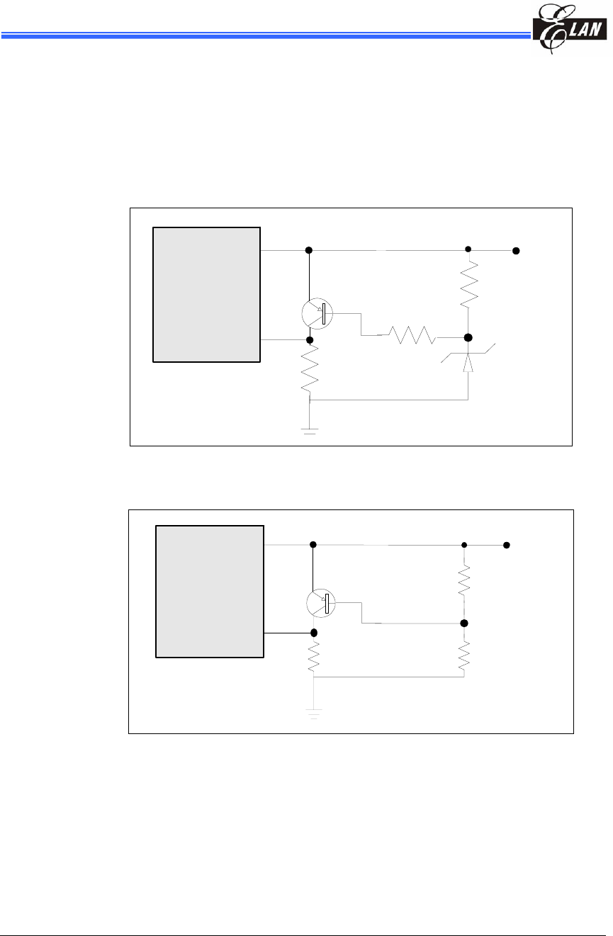
EM78P259N/260N
8-Bit Microprocessor with OTP ROM
66 • Product Specification (V1.2) 05.18.2007
(This specification is subject to change without further notice)
6.12.3 Residual Voltage Protection
When the battery is replaced, device power (Vdd) is removed but the residual voltage
remains. The residual voltage may trip below Vdd minimum, but not to zero. This
condition may cause a poor power-on reset. Fig. 6-22 and Fig. 6-23 show how to
create a protection circuit against residual voltage.
EM78P259N
EM78P260N
/RESET
Vdd
100K
Q1
1N4684
10K
33K
Vdd
Fig. 6-22 Residual Voltage Protection Circuit 1
/RESET
Vdd
Q1
Vdd
R3 R2
R1
EM78P259N
EM78P260N
Fig. 6-23 Residual Voltage Protection Circuit 2
EM78P259N/260N
8-Bit Microprocessor with OTP ROM
Product Specification (V1.2) 05.18.2007 • 67
(This specification is subject to change without further notice)
6.13 Code Option
EM78P259N/260N has two Code option words and one Customer ID word that are not
part of the normal program memory.
Word 0 Word1 Word 2
Bit12 ~ Bit0 Bit12 ~ Bit0 Bit12 ~ Bit0
6.13.1 Code Option Register (Word 0)
Word 0
Bit 12 Bit 11 Bit 10 Bit 9 Bit 8 Bit 7 Bit 6 Bit 5 Bit 4 Bit 3 Bit 2 Bit 1 Bit 0
– – – TYPE CLKS ENWDTB OSC2 OSC1 OSC0 HLP PR2 PR1 PR0
Bits 12 ~ 10: Not used (reserved). These bits are set to “1” all the time
Bit 9 (TYPE): Type selection for EM78P259N or EM78P260N
0 = EM78P260N
1 = EM78P259N (default)
Bit 8 (CLKS): Instruction period option bit
0 = two oscillator periods
1 = four oscillator periods (default)
Refer to Section 6.15 for Instruction Set
Bit 7 (ENWDTB): Watchdog timer enable bit
0 = Enable
1 = Disable (default)
Bits 6, 5 & 4 (OSC2, OSC1 & OSC0): Oscillator Mode Selection bits
Oscillator Modes OSC2 OSC1 OSC0
ERC1 (External RC oscillator mode); P70/OSCO acts as P70 0 0 0
ERC1 (External RC oscillator mode); P70/OSCO acts as OSCO 0 0 1
IRC2 (Internal RC oscillator mode); P70/OSCO acts as P70 0 1 0
IRC2 (Internal RC oscillator mode); P70/OSCO acts as OSCO 0 1 1
LXT3 (Low Crystal oscillator mode) 1 1 0
HXT3 High Crystal oscillator mode) (default) 1 1 1
1 In ERC mode, OSCI is used as oscillator pin. OSCO/P70 is defined by code option Word 0 Bit 6 ~ Bit 4.
2 In IRC mode, P55 is normal I/O pin. OSCO/P70 is defined by code option Word 0 Bit 6 ~ Bit 4.
3 In LXT and HXT modes; OSCI and OSCO are used as oscillator pins. These pins cannot and
should not be defined as normal I/O pins.
NOTE
The transient point of the system frequency between HXT and LXY is around 400kHz.
EM78P259N/260N
8-Bit Microprocessor with OTP ROM
68 • Product Specification (V1.2) 05.18.2007
(This specification is subject to change without further notice)
Bit 3 (HLP): Power consumption selection
0 = Low power consumption, applies to working frequency
at or below 4MHz
1 = High power consumption, applies to working frequency
above 4MHz
Bit 2 ~ 0 (PR2 ~ PR0): Protect Bits
PR2 ~ PR0 are protect bits. Each protect status is as follows:
PR2 PR1 PR0 Protect
Others Enable
1 1 1 Disable
6.13.2 Code Option Register (Word 1)
Word 1
Bit 12 Bit 11 Bit 10 Bit 9 Bit 8 Bit 7 Bit 6 Bit 5 Bit 4 Bit 3 Bit 2 Bit 1 Bit 0
- - RCOUT NRHL NRE WDTPS CYES C3 C2 C1 C0 RCM1 RCM0
Bits 12 ~ 11: Not used (reserved). These bits are set to “1” all the time
Bit 10 (RCOUT): Instruction clock output enable bit in IRC or ERC mode
0 = OSCO pin is open drain
1 = OSCO output instruction clock
Bit 9 (NRHL): Noise rejection high/low pulses define bit. INT pin is falling or
rising edge trigger
0 = Pulses equal to 8/fc [s] is regarded as signal
1 = Pulses equal to 32/fc [s] is regarded as signal (default)
NOTE
The noise rejection function is turned off under the LXT and sleep mode.
Bit 8 (NRE): Noise rejection enable
0 = disable noise rejection
1 = enable noise rejection (default), but under Low Crystal
oscillator (LXT) mode, the noise rejection circuit is always
disabled.
EM78P259N/260N
8-Bit Microprocessor with OTP ROM
Product Specification (V1.2) 05.18.2007 • 69
(This specification is subject to change without further notice)
Bit 7 (WDTPS): WDT Time-out Period Selection bit
WDT Time Watchdog Time*
1 18 ms
0 4.5 ms
*These are theoretical values provided for reference only
Bit 6 (CYES): Instruction cycle selection bit
0 = one instruction cycle.
1 = two instructions cycles (default)
Bits 5, 4, 3, & Bit 2 (C3, C2, C1, C0): Calibrator of internal RC mode
C3, C2, C1, & C0 must be set to “1” only (auto-calibration).
Bit 1 & Bit 0 (RCM1, RCM0): RC mode selection bits
RCM 1 RCM 0 Frequency (MHz)
1 1 4
1 0 8
0 1 1
0 0 455kHz
6.13.3 Customer ID Register (Word 2)
Word 2
Bit 12 Bit 11 Bit 10 Bit 9 Bit 8 Bit 7 Bit 6 Bit 5 Bit 4 Bit 3 Bit 2 Bit 1 Bit 0
X X X X X X X X X X X X X
Bit 12 ~ 0: Customer’s ID code
6.14 Instruction Set
Each instruction in the instruction set is a 13-bit word divided into an OP code and one
or more operands. Normally, all instructions are executed within one single instruction
cycle (one instruction consists of 2 oscillator periods), unless the program counter is
changed by instructions "MOV R2,A," "ADD R2,A," or by instructions of arithmetic or
logic operation on R2 (e.g., "SUB R2,A," "BS(C) R2,6," "CLR R2," etc.). In this case,
these instructions need one or two instruction cycles as determined by Code Option
Register CYES bit.
In addition, the instruction set has the following features:
1. Every bit of any register can be set, cleared, or tested directly.
2. The I/O registers can be regarded as general registers. That is, the same
instruction can operate on I/O registers.

EM78P259N/260N
8-Bit Microprocessor with OTP ROM
70 • Product Specification (V1.2) 05.18.2007
(This specification is subject to change without further notice)
Convention:
R = Register designator that specifies which one of the registers (including operation and general purpose
registers) is to be utilized by the instruction.
b = Bit field designator that selects the value for the bit located in the register R and which affects the
operation.
k = 8 or 10-bit constant or literal value
The following are the EM78P259N/260N instruction set
Instruction Binary HEX Mnemonic Operation Status Affected
0 0000 0000 0000 0000 NOP No Operation None
0 0000 0000 0001 0001 DAA Decimal Adjust A C
0 0000 0000 0010 0002 CONTW A → CONT None
0 0000 0000 0011 0003 SLEP 0 → WDT, Stop oscillator T, P
0 0000 0000 0100 0004 WDTC 0 → WDT T, P
0 0000 0000 rrrr 000r IOW R A → IOCR None1
0 0000 0001 0000 0010 ENI Enable Interrupt None
0 0000 0001 0001 0011 DISI Disable Interrupt None
0 0000 0001 0010 0012 RET [Top of Stack] → PC None
0 0000 0001 0011 0013 RETI [Top of Stack] → PC, Enable Interrupt None
0 0000 0001 0100 0014 CONTR CONT → A None
0 0000 0001 rrrr 001r IOR R IOCR → A None1
0 0000 01rr rrrr 00rr MOV R,A A → R None
0 0000 1000 0000 0080 CLRA 0 → A Z
0 0000 11rr rrrr 00rr CLR R 0 → R Z
0 0001 00rr rrrr 01rr SUB A,R R-A → A Z, C, DC
0 0001 01rr rrrr 01rr SUB R,A R-A → R Z, C, DC
0 0001 10rr rrrr 01rr DECA R R-1 → A Z
0 0001 11rr rrrr 01rr DEC R R-1 → R Z
0 0010 00rr rrrr 02rr OR A,R A ∨ VR → A Z
0 0010 01rr rrrr 02rr OR R,A A ∨ VR → R Z
0 0010 10rr rrrr 02rr AND A,R A & R → A Z
0 0010 11rr rrrr 02rr AND R,A A & R → R Z
0 0011 00rr rrrr 03rr XOR A,R A ⊕ R → A Z
0 0011 01rr rrrr 03rr XOR R,A A ⊕ R → R Z
0 0011 10rr rrrr 03rr ADD A,R A + R → A Z, C, DC
0 0011 11rr rrrr 03rr ADD R,A A + R → R Z, C, DC
0 0100 00rr rrrr 04rr MOV A,R R → A Z
0 0100 01rr rrrr 04rr MOV R,R R → R Z
0 0100 10rr rrrr 04rr COMA R /R → A Z
0 0100 11rr rrrr 04rr COM R /R → R Z
0 0101 00rr rrrr 05rr INCA R R+1 → A Z

EM78P259N/260N
8-Bit Microprocessor with OTP ROM
Product Specification (V1.2) 05.18.2007 • 71
(This specification is subject to change without further notice)
Instruction Binary HEX Mnemonic Operation Status Affected
0 0101 01rr rrrr 05rr INC R R+1 → R Z
0 0101 10rr rrrr 05rr DJZA R R-1 → A, skip if zero None
0 0101 11rr rrrr 05rr DJZ R R-1 → R, skip if zero None
0 0110 00rr rrrr 06rr RRCA R R(n) → A(n-1),R(0) → C, C → A(7) C
0 0110 01rr rrrr 06rr RRC R R(n) → R(n-1),R(0) → C, C → R(7) C
0 0110 10rr rrrr 06rr RLCA R R(n) → A(n+1),R(7) → C, C → A(0) C
0 0110 11rr rrrr 06rr RLC R R(n) → R(n+1),R(7) → C, C → R(0) C
0 0111 00rr rrrr 07rr SWAPA R R(0-3) → A(4-7),R(4-7) → A(0-3) None
0 0111 01rr rrrr 07rr SWAP R R(0-3) ↔ R(4-7) None
0 0111 10rr rrrr 07rr JZA R R+1 → A, skip if zero None
0 0111 11rr rrrr 07rr JZ R R+1 → R, skip if zero None
0 100b bbrr rrrr 0xxx BC R,b 0 → R(b) None2
0 101b bbrr rrrr 0xxx BS R,b 1 → R(b) None3
0 110b bbrr rrrr 0xxx JBC R,b if R(b)=0, skip None
0 111b bbrr rrrr 0xxx JBS R,b if R(b)=1, skip None
1 00kk kkkk kkkk 1kkk CALL k PC+1 → [SP],(Page, k) → PC None
1 01kk kkkk kkkk 1kkk JMP k (Page, k) → PC None
1 1000 kkkk kkkk 18kk MOV A,k k → A None
1 1001 kkkk kkkk 19kk OR A,k A ∨ k → A Z
1 1010 kkkk kkkk 1Akk AND A,k A & k → A Z
1 1011 kkkk kkkk 1Bkk XOR A,k A ⊕ k → A Z
1 1100 kkkk kkkk 1Ckk RETL k k → A,[Top of Stack] → PC None
1 1101 kkkk kkkk 1Dkk SUB A,k k-A → A Z, C, DC
1 1111 kkkk kkkk 1Fkk ADD A,k k+A → A Z, C, DC
1 This instruction is applicable to IOC50 ~ IOCF0, IOC51 ~ IOCC1 only.
2 This instruction is not recommended for RF operation.
3 This instruction cannot operate under RF.
7 Absolute Maximum Ratings
Items Rating
Temperature under bias -40°C to 85°C
Storage temperature -65°C to 150°C
Input voltage Vss-0.3V to Vdd+0.5V
Output voltage Vss-0.3V to Vdd+0.5V
Working Voltage 2.5V to 5.5V
Working Frequency DC to 20MHz

EM78P259N/260N
8-Bit Microprocessor with OTP ROM
72 • Product Specification (V1.2) 05.18.2007
(This specification is subject to change without further notice)
8 DC Electrical Characteristics
Ta=25 °C, VDD=5.0V±5%, VSS=0V
Symbol Parameter Condition Min Typ Max Unit
Crystal: VDD to 5V DC 20 MHz
Crystal: VDD to 3V
Two cycles with two clocks
DC 8 MHz
Fxt
ERC: VDD to 5V R: 5.1KΩ, C: 100 pF F±30% 830 F±30% kHz
VIHRC Input High Threshold
Voltage (Schmitt trigger) OSCI in RC mode 3.5 V
VILRC Input Low Threshold
Voltage (Schmitt trigger) OSCI in RC mode 1.5 V
IIL Input Leakage Current for
input pins VIN = VDD, VSS -1 0 1 μA
VIH1 Input High Voltage
(Schmitt trigger) Ports 5, 6, 7 3.75 V
VIL1 Input Low Voltage
(Schmitt trigger) Ports 5, 6, 7 1.25 V
VIHT1 Input High Threshold
Voltage (Schmitt trigger) /RESET 2.0 V
VILT1 Input Low Threshold
Voltage (Schmitt trigger) /RESET 1.0 V
VIHT2 Input High Threshold
Voltage (Schmitt trigger) TCC, INT 3.75 V
VILT2 Input Low Threshold
Voltage (Schmitt trigger) TCC, INT 1.25 V
VIHX1 Clock Input High Voltage OSCI in crystal mode 3.5 V
VILX1 Clock Input Low Voltage OSCI in crystal mode 1.5 V
IOH1 Output High Voltage
(Ports 5, P60~66, P70) VOH = VDD-0.5V -3.7 mA
IOH2 Output High Voltage
(IR OUT (Port67)) VOH = VDD-0.5V -10 mA
IOL1 Output Low Voltage
(Ports 5, P60~66, P70) VOL = GND+0.5V 10 mA
IOL2 Output Low Voltage
(IR OUT (Port 67)) VOL = GND+0.5V 15 mA
IPH Pull-high current Pull-high active, input pin at VSS -70 -75 -80 μA
IPL Pull-low current Pull-low active, input pin at Vdd 35 40 45 μA
ISB1 Power down current All input and I/O pins at VDD,
Output pin floating, WDT disabled 1.0 2.0 μA
ISB2 Power down current All input and I/O pins at VDD,
Output pin floating, WDT enabled 6.0 10 μA

EM78P259N/260N
8-Bit Microprocessor with OTP ROM
Product Specification (V1.2) 05.18.2007 • 73
(This specification is subject to change without further notice)
Symbol Parameter Condition Min Typ Max Unit
ICC1 Operating supply current
at two clocks (VDD to 3V)
/RESET= 'High', Fosc=32kHz
(Crystal type,CLKS="0"), output
pin floating, WDT disabled
15 20 μA
ICC2 Operating supply current
at two clocks (VDD to 3V)
/RESET= 'High', Fosc=32kHz
(Crystal type,CLKS="0"), output
pin floating, WDT enabled
15 25 μA
ICC3 Operating supply current
at two clocks
/RESET= 'High', Fosc=4MHz
(Crystal type, CLKS="0"), output
pin floating, WDT enabled
1.9 2.2 mA
ICC4 Operating supply current
at two clocks
/RESET= 'High', Fosc=10MHz
(Crystal type, CLKS="0"), output
pin floating, WDT enabled
3.0 3.5 mA
Note: These parameters are hypothetical, have not been tested and are provided for design reference only.
Data in the Minimum, Typical and Maximum (“Min”, Typ”, Max”) columns are based on hypothetical
results at 25°C. These data are for design reference only.
Internal RC Electrical Characteristics (Ta=25°C, VDD=5 V, VSS=0V)
Drift Rate
Internal RC Temperature Voltage Min. Typ. Max.
4MHz 25°C 5V 3.84MHZ 4MHz 4.16MHz
8MHz 25°C 5V 7.68MHz 8MHz 8.32MHz
1MHz 25°C 5V 0.96MHz 1MHz 1.04MHz
455kHz 25°C 5V 436.8kHz 455kHz 473.2kHz
Internal RC Electrical Characteristics (Ta=-40 ~85°C, VDD=2.2~5.5 V, VSS=0V)
Drift Rate
Internal RC Temperature Voltage Min. Typ. Max.
4MHz -40°C ~85°C 2.2V~5.5 V 3.24MHZ 4MHz 4.76MHz
8MHz -40°C ~85°C 2.2V~5.5 V 6.4MHz 8MHz 9.6MHz
1MHz -40°C ~85°C 2.2V~5.5 V 0.81MHz 1MHz 1.19MHz
455kHz -40°C ~85°C 2.2V~5.5 V 368.55kHz 455kHz 541.45kHz

EM78P259N/260N
8-Bit Microprocessor with OTP ROM
74 • Product Specification (V1.2) 05.18.2007
(This specification is subject to change without further notice)
8.1 AD Converter Characteristics
Vdd=2.5V to 5.5V, Vss=0V, Ta=25°C
Symbol Parameter Condition Min. Typ. Max. Unit
VAREF 2.5 – Vdd V
VASS
Analog reference voltage VAREF - VASS ≥ 2.5V
Vss – Vss V
VAI Analog input voltage – VASS – VAREF V
Ivdd 750 850 1000 uA
IAI1 Ivref Analog supply current Vdd=VAREF=5.0V, VASS =0.0V
(V reference from Vdd) –10 0 +10 uA
Ivdd 500 600 820 uA
IAI2 IVref Analog supply current Vdd=VAREF=5.0V, VASS=0.0V
(V reference from VREF) 200 250 300 uA
IOP OP current Vdd=5.0V, OP used
Output voltage swing 0.2V to 4.8V 450 550 650 uA
RN1 Resolution VREFS=0, Internal VDD
VDD=5.0V, VSS = 0.0V − 9 10 Bits
RN2 Resolution VREFS=1, External VREF
VDD=VREF=5.0V, VSS = 0.0V − 11 12 Bits
LN1 Linearity error Vdd = 2.5 to 5.5V Ta=25°C 0 ±4 ±8 LSB
LN2 Linearity error VDD= 2.5 to 5.5V Ta=25°C 0 ±2 ±4 LSB
DNL Differential nonlinear error Vdd = 2.5 to 5.5V Ta=25°C 0 ±0.5 ±0.9 LSB
FSE1 Full scale error Vdd=VAREF=5.0V, VASS =0.0V ±0 ±4 ±8 LSB
FSE2 Full scale error VDD=VREF=5.0V, VSS = 0.0V ±0 ±2 ±4 LSB
OE Offset error Vdd=VAREF=5.0V, VASS =0.0V ±0 ±2 ±4 LSB
ZAI Recommended impedance of
analog voltage source – 0 8 10 KΩ
TAD ADC clock period Vdd=VAREF=5.0V, VASS =0.0V 4 – – μs
TCN AD conversion time Vdd=VAREF=5.0V, VASS =0.0V 15 – 15 TAD
ADIV ADC OP input voltage range Vdd=VAREF=5.0V, VASS =0.0V 0 – VAREF V
0 0.2 0.3
ADOV ADC OP output voltage swing Vdd=VAREF=5.0V, VASS
=0.0V,RL=10KΩ 4.7 4.8 5 V
ADSR ADC OP slew rate Vdd=VAREF=5.0V, VASS =0.0V 0.1 0.3 – V/us
TAD A/D clock period VDD=VREF=5.0V, VSS = 0.0V 4 − − µs
TCN A/D conversion time VDD=VREF=5.0V, VSS = 0.0V 15 − 15 TAD
PSR Power Supply Rejection Vdd=5.0V±0.5V ±0 – ±2 LSB
Note: 1. These parameters are hypothetical, have not been tested and are provided for design reference only.
2. There is no current consumption when ADC is off other than minor leakage current.
3. AD conversion result will not decrease when an increase of input voltage and no missing code will result.
EM78P259N/260N
8-Bit Microprocessor with OTP ROM
Product Specification (V1.2) 05.18.2007 • 75
(This specification is subject to change without further notice)
8.2 Comparator (OP) Characteristics
Vdd = 5.0V, Vss=0V, Ta=25°C
Symbol Parameter Condition Min. Typ. Max. Unit
SR Slew rate - 0.1 0.2 - V/us
Vos Input offset voltage - - - 30 mV
IVR Input voltage range Vdd =5.0V, VSS =0.0V 0 5 V
0 0.2 0.3
OVS Output voltage swing
Vd =5.0V, VSS =0.0V,
RL=10KΩ 4.7 4.8 5 V
Iop Supply current of OP - 250 350 500 uA
Ico Supply current of
Comparator - - 300 - uA
PSRR Power-supply Rejection
Ration for OP
Vdd= 5.0V,
VSS =0.0V 50 60 70 dB
Vs Operating range - 2.5 - 5.5 V
Note: These parameters are hypothetical (not tested) and are provided for design reference only.
8.3 Device Characteristics
The graphs below were derived based on a limited number of samples and they are
provided for reference only. Hence, the device characteristic shown herein cannot be
guaranteed as fully accurate. In these graphs, the data maybe out of the specified
operating warranted range.
IRC OSC Frequency (VDD=3V)
0
1
2
3
4
5
6
7
8
9
-40-200 25507085
Temperature (℃)
Frequency (M Hz)
Fig. 8-1 Internal RC OSC Frequency vs. Temperature, VDD=3V
EM78P259N/260N
8-Bit Microprocessor with OTP ROM
76 • Product Specification (V1.2) 05.18.2007
(This specification is subject to change without further notice)
I RC OSC Frequency (VDD=5V)
0
1
2
3
4
5
6
7
8
9
10
-40-200 25507085
Temper at ur e (℃ )
Frequency (M Hz)
Fig. 8-2 Internal RC OSC Frequency vs. Temperature, VDD=5V
9 AC Electrical Characteristic
Ta=25°C, VDD=5V±5%, VSS=0V
Symbol Parameter Conditions Min Typ Max Unit
Dclk Input CLK duty cycle 45 50 55 %
Crystal type 100 DC ns
Tins Instruction cycle time
(CLKS="0") RC type 500 DC ns
Ttcc TCC input period (Tins+20)/N* ns
Tdrh Device reset hold time Ta = 25°C 11.3 16.2 21.6 ms
Trst /RESET pulse width Ta = 25°C 2000 ns
Twdt Watchdog timer period
Ta = 25°C 11.3 16.2 21.6 ms
Tset Input pin setup time 0 ns
Thold Input pin hold time 15 20 25 ns
Tdelay Output pin delay time Cload=20pF 45 50 55 ns
Tdrc ERC delay time Ta = 25°C 1 3 5 ns
Note: 1. N = selected prescaler ratio
2. Twdt1: The Option Word1 (WDTPS) is used to define the oscillator set-up time. WDT timeout length is
the same as set-up time (18ms).
3. Twdt2: The Option Word1 (WDTPS) is used to define the oscillator set-up time. WDT timeout length is
the same as set-up time (4.5ms).
4. These parameters are hypothetical (not tested) and are provided for design reference only.
5. Data under minimum, typical, & maximum (Min, Typ, & Max) columns are based on hypothetical results at 25°C.
These data are for design reference use only.
6. The Watchdog timer duration is determined by Code Option Word1 (WDTPS).
EM78P259N/260N
8-Bit Microprocessor with OTP ROM
Product Specification (V1.2) 05.18.2007 • 77
(This specification is subject to change without further notice)
10 Timing Diagrams
RESET Timing (CLK="0")
CLK
/RESET
NOP Instruction 1
Executed
Tdrh
TCC Input Timing (CLKS="0")
CLK
TCC
Ttcc
Tins
AC Testing : Input is driven at VDD-0.5V for logic "1",and GND+0.5V for logic "0".Timing
measurements are made at 0.75VDD for logic "1",and 0.25VDD for logic "0".
AC Test Input/Output Waveform
VDD-0.5V
GND+0.5V
0.75VDD
0.25VDDTEST POINTS 0.75VDD
0.25VDD
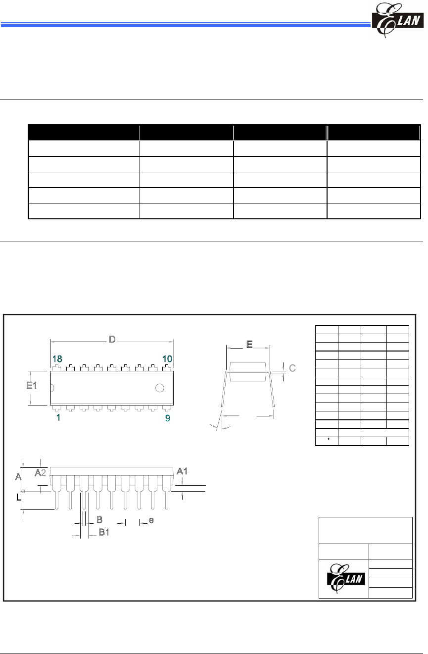
EM78P259N/260N
8-Bit Microprocessor with OTP ROM
78 • Product Specification (V1.2) 05.18.2007
(This specification is subject to change without further notice)
APPENDIX
A Package Type
OTP MCU Package Type Pin Count Package Size
EM78P259NPS/NPJ DIP 18 300mil
EM78P259NMS/NMJ SOP 18 300mil
EM78P260NPS/NPJ DIP 20 300mil
EM78P260NMS/NMJ SOP 20 300mil
EM78P260NKMS/NKMJ SSOP 20 209mil
B Package Information
B.1 18-Lead Plastic Dual in line (PDIP) — 300 mil
TITLE:
PDI P-18L 300MI L PACKAGE
OUTLINE DIMENSION
Unit : mm
Scale: Free
File :
D18
Material:
Edtion: A
Sheet:1 of 1
Min Normal Max
4.450
0.381
3.175 3.302 3.429
0.203 0.254 0.356
22.610 22.860 23.110
6.220 6.438 6.655
7.370 7.620 7.870
8.510 9.020 9.530
0.356 0.457 0.559
1.143 1.524 1.778
3.048 3.302 3.556
2.540(TYP)
015
Symbal
A
A1
A2
c
D
E1
E
eB
B
B1
L
e
θ
θ
eB
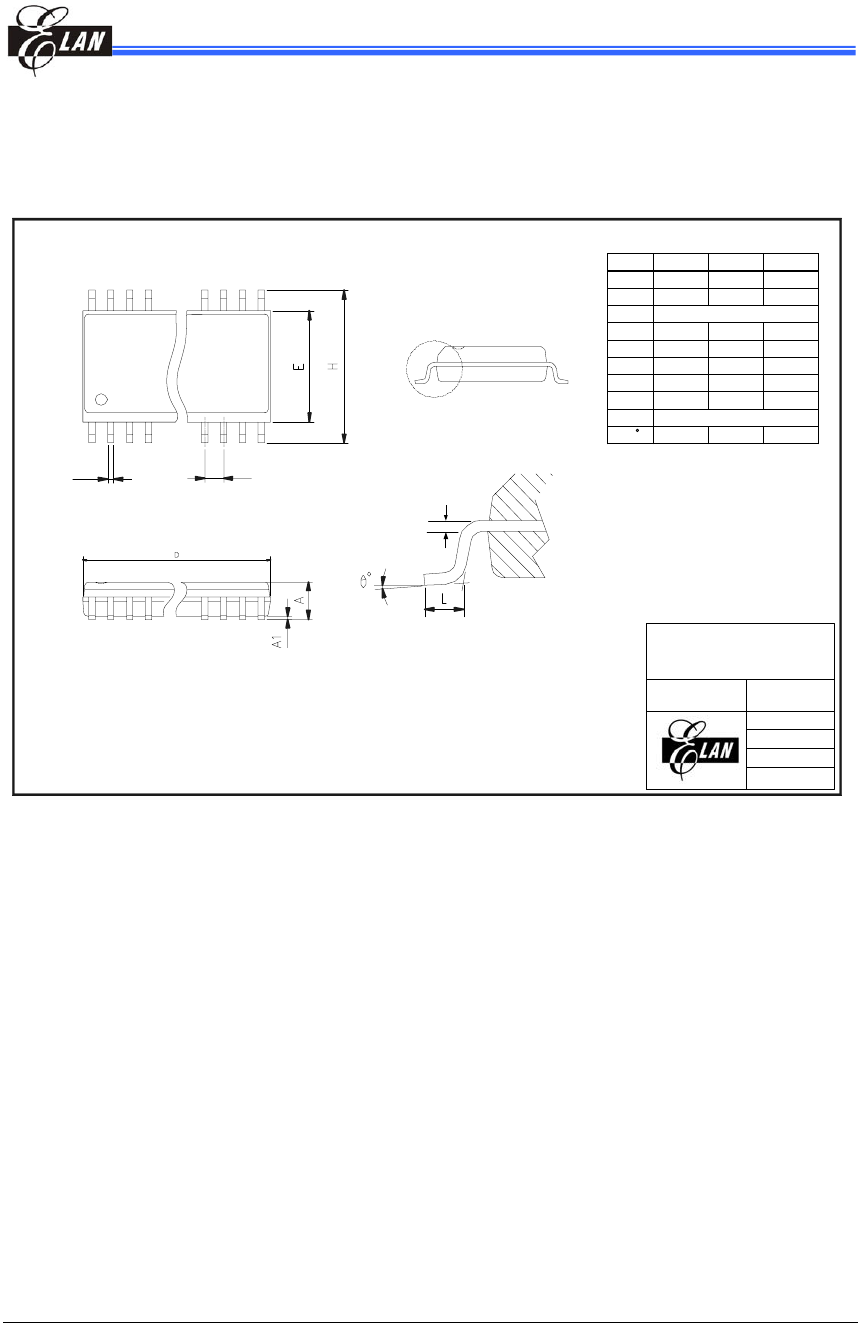
EM78P259N/260N
8-Bit Microprocessor with OTP ROM
Product Specification (V1.2) 05.18.2007 • 79
(This specification is subject to change without further notice)
B.2 18-Lead Plastic Small Outline (SOP) — 300 mil
TITLE:
SOP-18L(300MIL) PACKAGE
OUTLINE DIMENSION
Unit : mm
Scale: Free
Material:
Edtion: A
Sheet:1 of 1
be
Min Normal Max
2.350 2.650
0.102 0.300
0.406(TYP)
0.230 0.320
7.400 7.600
10.000 10.650
11.350 11.750
0.406 0.838 1.270
1.27(TYP)
08
Symbal
A
A1
b
c
E
H
D
L
e
θ
c
File :
SO18
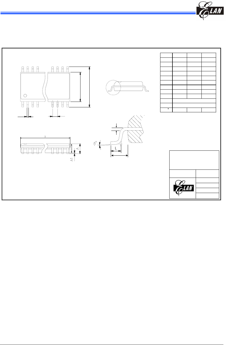
EM78P259N/260N
8-Bit Microprocessor with OTP ROM
80 • Product Specification (V1.2) 05.18.2007
(This specification is subject to change without further notice)
B.3 20-Lead Plastic Shrink Small Outline (SSOP) — 209 mil
TITLE:
SSOP-20L(209MIL) OUTLINE
PACKAGE PACKA OUTLINE
DIMENSION
Unit : mm
Scale: Free
File :
SSOP20
Material:
Edtion: A
Sheet:1 of 1
be
c
E
E1
A2
Min Normal Max
2.130
0.050 0.250
1.620 1.750 1.880
0.220 0.380
0.090 0.200
7.400 7.800 8.200
5.000 5.300 5.600
6.900 7.200 7.500
0.650 0.750 0.850
1.250(REF )
0.650(TYP)
0
4
8
Symbal
A
A1
A2
b
c
E
E1
D
L
L1
e
θ
L1
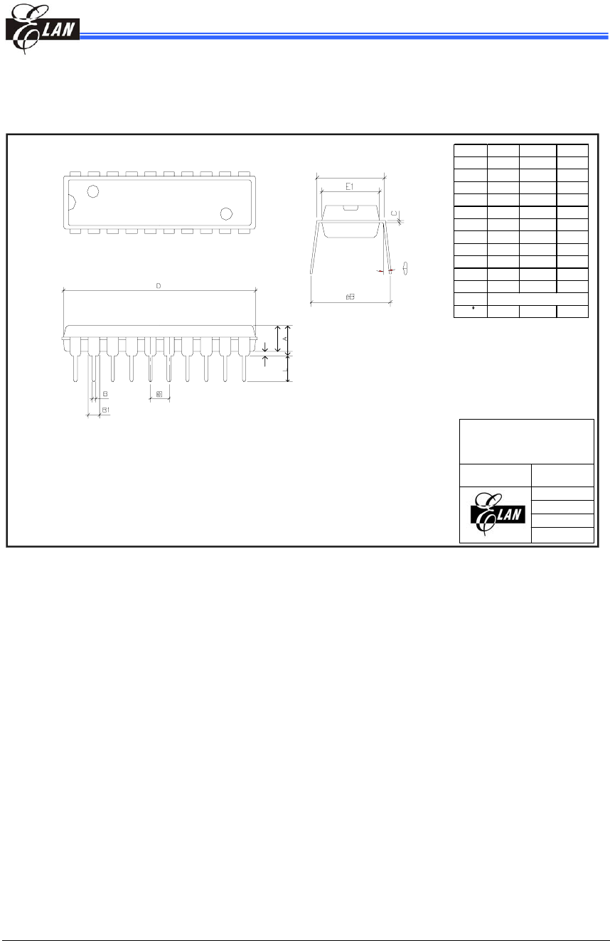
EM78P259N/260N
8-Bit Microprocessor with OTP ROM
Product Specification (V1.2) 05.18.2007 • 81
(This specification is subject to change without further notice)
B.4 20-Lead Plastic Dual-in-line (PDIP) — 300 mil
TITLE:
PDIP-20L 300MIL PACKAGE
OUTLINE DIMENSION
Unit : mm
Scale: Free
File :
D20
Material:
Edtion: A
Sheet:1 of 1
Min Normal Max
4.450
0.381
3.175 3.302 3.429
0.203 0.254 0.356
25.883 26.060 26.237
6.220 6.438 6.655
7.370 7.620 7.870
8.510 9.020 9.530
0.356 0.457 0.559
1.143 1.524 1.778
3.048 3.302 3.556
2.540(TYP)
01
5
Symbal
A
A1
A2
c
D
E1
E
eB
B
B1
L
e
θ
A2
A1
E
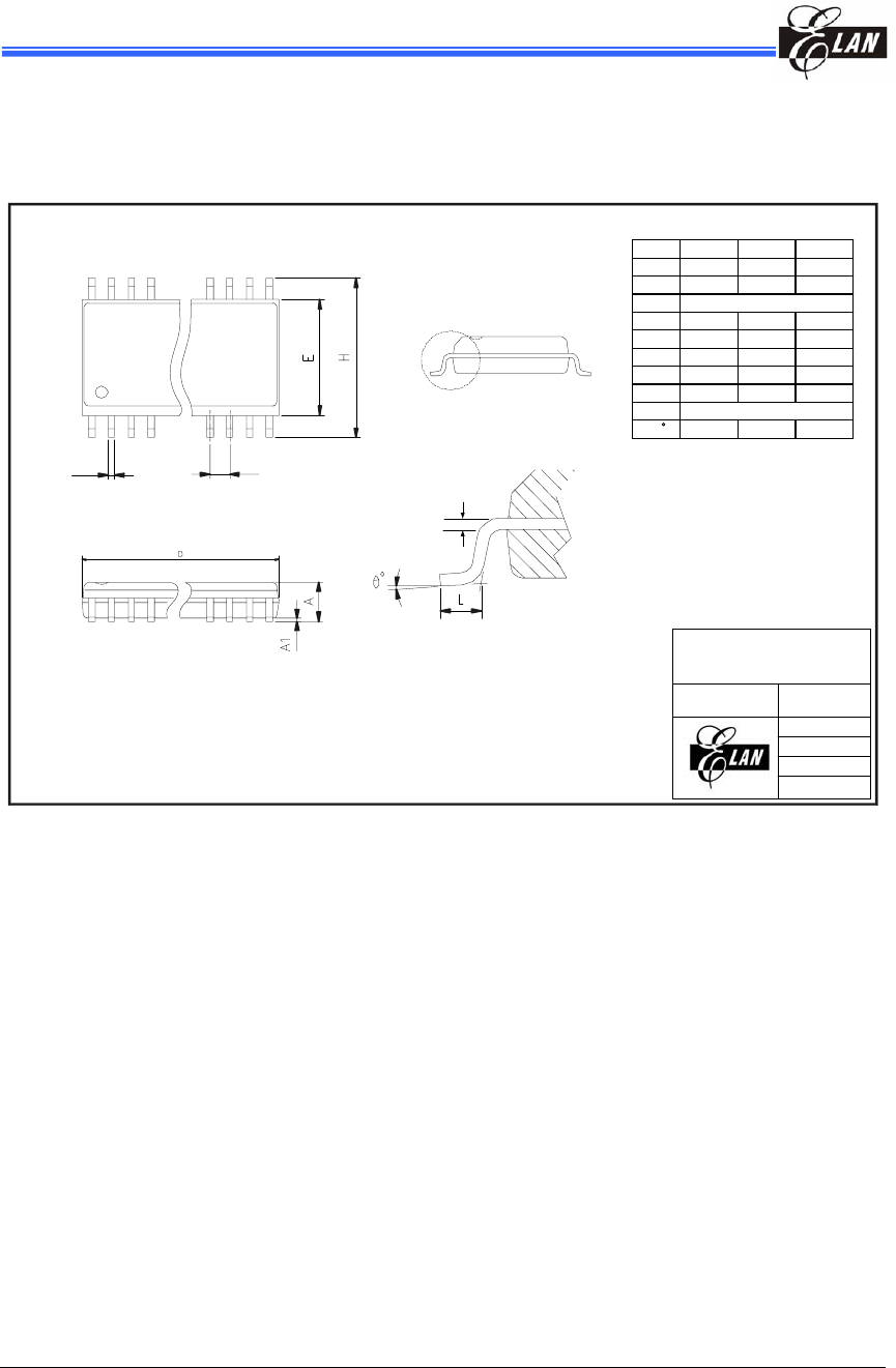
EM78P259N/260N
8-Bit Microprocessor with OTP ROM
82 • Product Specification (V1.2) 05.18.2007
(This specification is subject to change without further notice)
B.5 20-Lead Plastic Small Outline (SOP) — 300 mil
TITLE:
SOP-20L(300MIL) PACKAGE
OUTLINE DIMENSION
Unit : mm
Scale: Free
File :
SO20
Material:
Edtion: A
Sheet:1 of 1
be
Symbal
A
A1
b
c
E
H
D
L
e
θ
c
Min Normal Max
2.350 2.650
0.102 0.300
0.406(TYP)
0.230 0.320
7.400 7.600
10.000 10.650
12.600 12.900
0.630 0.838 1.100
1.27(TYP)
0
8

EM78P259N/260N
8-Bit Microprocessor with OTP ROM
Product Specification (V1.2) 05.18.2007 • 83
(This specification is subject to change without further notice)
C Quality Assurance and Reliability
Test Category Test Conditions Remarks
Solderability Solder temperature=245±5°C, for 5 seconds up to the
stopper using a rosin-type flux
Step 1: TCT, 65°C (15mins)~150°C (15mins), 10 cycles
Step 2: Bake at 125°C, TD (durance)=24 hrs
Step 3: Soak at 30°C/60%,TD (durance)=192 hrs
Pre-condition Step 4: IR flow 3 cycles
(Pkg thickness ≥ 2.5mm or
Pkg volume ≥ 350mm3 ----225±5°C)
(Pkg thickness ≤ 2.5mm or
Pkg volume ≤ 350mm3 ----240±5°C )
For SMD IC (such as
SOP, QFP, SOJ, etc)
Temperature cycle test -65℃ (15mins)~150°C (15mins), 200 cycles
Pressure cooker test TA =121°C, RH=100%, pressure=2 atm,
TD (durance)= 96 hrs
High temperature /
High humidity test TA=85°C , RH=85%,TD (durance)=168 , 500 hrs
High-temperature
storage life TA=150°C, TD (durance)=500, 1000 hrs
High-temperature
operating life
TA=125°C, VCC=Max. operating voltage,
TD (durance) =168, 500, 1000 hrs
Latch-up TA=25°C, VCC=Max. operating voltage, 150mA/20V
ESD (HBM) TA=25°C, ≥∣± 3KV∣
ESD (MM) TA=25℃, ≥∣± 300V∣
IP_ND,OP_ND,IO_ND
IP_NS,OP_NS,IO_NS
IP_PD,OP_PD,IO_PD,
IP_PS,OP_PS,IO_PS,
VDD-VSS(+),VDD_VSS
(-)mode
C.1 Address Trap Detect
An address trap detect is one of the MCU embedded fail-safe functions that detects
MCU malfunction caused by noise or the like. Whenever the MCU attempts to fetch an
instruction from a certain section of ROM, an internal recovery circuit is auto started. If
a noise caused address error is detected, the MCU will repeat execution of the program
until the noise is eliminated. The MCU will then continue to execute the next program.
