Ibm Network Card Ds 2000 Users Manual C
DS-2000 to the manual cb0b47e2-72cd-4b04-8d3a-3c7419a450ad
2015-03-11
: Ibm Ibm-Ibm-Network-Card-Ds-2000-Users-Manual-577207 ibm-ibm-network-card-ds-2000-users-manual-577207 ibm pdf
Open the PDF directly: View PDF ![]() .
.
Page Count: 27

WARRANTY INFORMATION
Qua Tech Inc. warrants the DS-2000 to be
free of defects for one (1) year from the date of
purchase. Qua Tech Inc. will repair or replace any board
that fails to perform under normal operating conditions
and in accordance with the procedures outlined in this
document during the warranty period. Any damage that
results from improper installation, operation, or general
misuse voids all warranty rights.
Although every attempt has been made to guarantee
the accuracy of this manual, Qua Tech Inc. assumes no
liability for damages resulting from errors in this
document. Qua Tech Inc. reserves the right to edit or
append to this document at any time without notice.
Please complete the following information and retain
for your records. Have this information available when
requesting warranty service.
DATE OF PURCHASE:
MODEL NUMBER: DS-2000
PRODUCT DESCRIPTION: DUAL CHANNEL RS-422 ASYNC.
COMMUNICATIONS ADAPTER
SERIAL NUMBER:
IBM PC/XT/ATTM, PS/2TM, and MicroChannelTM are trademarks
of International Business Machines.
i
TABLE OF CONTENTS
WARRANTY INFORMATION . . . . . . . . . . . . i
LIST OF FIGURES . . . . . . . . . . . . . iii
I. INTRODUCTION . . . . . . . . . . . . . . . . 1
II. BOARD DESCRIPTION . . . . . . . . . . . . . 1
III. 16550 FUNCTIONAL DESCRIPTION . . . . . . . . 3
A. INTERRUPT ENABLE REGISTER . . . . . . . . 4
B. INTERRUPT IDENTIFICATION REGISTER . . . . 5
C. FIFO CONTROL REGISTER . . . . . . . . . . 7
D. LINE CONTROL REGISTER . . . . . . . . . . 8
E. MODEM CONTROL REGISTER . . . . . . . . . 10
F. LINE STATUS REGISTER . . . . . . . . . . 11
G. MODEM STATUS REGISTER . . . . . . . . . . 13
H. SCRATCHPAD REGISTER . . . . . . . . . . . 14
IV. FIFO INTERRUPT MODE OPERATION . . . . . . . 14
V. BAUD RATE SELECTIONS . . . . . . . . . . . . 14
VI. ADDRESSING . . . . . . . . . . . . . . . . . 16
VII. INTERRUPTS . . . . . . . . . . . . . . . . . 16
VIII. PROGRAMMABLE OPTION SELECT . . . . . . . . . 16
IX. OUTPUT CONFIGURATIONS . . . . . . . . . . . 19
X. EXTERNAL CONNECTIONS . . . . . . . . . . . . 23
XI. INSTALLATION . . . . . . . . . . . . . . . . 24
XII. SPECIFICATIONS . . . . . . . . . . . . . . . 24
i
LIST OF FIGURES
Figure 1. DS-2000 board layout . . . . . . . . . 2
Figure 2. 16550 internal registers . . . . . . . 3
Figure 3. Interrupt enable register . . . . . . 4
Figure 4. Interrupt identification register . . 5
Figure 5. Interrupt source identification . . . 6
Figure 6. FIFO control register . . . . . . . . 7
Figure 7. FIFO receiver trigger levels . . . . . 7
Figure 8. Line control register . . . . . . . . 8
Figure 9. Parity options . . . . . . . . . . . . 9
Figure 10. Word length and stop bit options . . . 9
Figure 11. MODEM control register . . . . . . . . 10
Figure 12. Line status register . . . . . . . . . 11
Figure 13. MODEM status register . . . . . . . . 13
Figure 14. Input clock frequency options . . . . 15
Figure 15. Divisor latch options . . . . . . . . 15
Figure 16. POS implementation . . . . . . . . . . 17
Figure 17. Base address locations . . . . . . . . 18
Figure 18. Interrupt request levels . . . . . . . 18
Figure 19. Output control block diagram . . . . . 21
Figure 20. J2/J3 layout and settings . . . . . . 21
Figure 21. Auxiliary channel configuration
(handshake mode) . . . . . . . . . 22
Figure 22. Auxiliary channel configuration
(external clock mode) . . . . . . . 22
Figure 23. Auxiliary channel configuration
(loopback mode) . . . . . . . . . . 22
Figure 24. Output connections . . . . . . . . . . 23
Figure 25. Output signal definitions . . . . . . 23
iii

I. INTRODUCTION
The DS-2000 is a dual channel asynchronous serial
communication adapter which utilizes balanced
differential drivers and receivers to provide RS-422-A
communications. It is capable of reliable communications
over long distances (4000 feet) within noisy industrial
environment. Data is communicated through two D-9
connectors which provide shielding from environmental
noise. Optional high speed transient suppressers may
also be installed on the DS-2000 to further reduce the
effects of environmental signal transients and surges.
The serial interface is accomplished through a pair
of 16550 Asynchronous Communication Elements (ACEs). The
16550 is compatible with the 8250 and 16450 ACEs used in
the IBM PC/XT/AT models. The 16550 also has an
additional FIFO mode that reduces CPU overhead at higher
data rates.
The DS-2000 supports sixteen base addresses for each
ACE through the Programmable Option Select (POS)
including the eight addresses designated SERIAL 1 through
SERIAL 8. The addresses are independent for each
channel. CPU interrupt level selections are also handled
through the POS. Each channel may select a separate
interrupt or share an interrupt level with other devices.
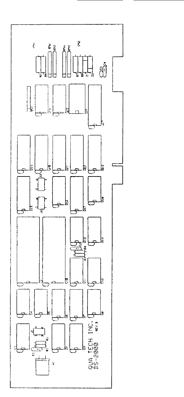
II. BOARD DESCRIPTION
A component diagram of the DS-2000 showing the
locations of the 16550 ACEs, configuration jumpers, and
D-9 connectors is shown in figure 1. The first
communication channel is controlled by the 16550 labeled
U9, jumper J2, and is accessed through the connector
labeled CN1. The second channel uses the 16550 labeled
U10, jumper J3, and is accessed through the connector
labeled CN2. The clock rate divider for both channels is
controlled by jumper J1.
iii
FUNCTIONAL DESCRIPTION
Figure 1. DS-2000 board layout.
iii

FUNCTIONAL DESCRIPTION
III. 16550 FUNCTIONAL DESCRIPTION
The 16550 is an upgrade of the standard 16450
Asynchronous Communications Element (ACE). Designed to
be compatible with the 16450, the 16550 enters the
character mode on reset and in this mode will appear as a
16450 to user software. An additional mode, FIFO mode,
can be selected to reduce CPU overhead at high data
rates. The FIFO mode increases performance by providing
two internal 16-byte FIFOs (one transmit and one receive)
to buffer data and reduce the number of interrupts issued
to the CPU.
Other features of the 16550 include:
Programmable baud rate, character length, parity,
and number of stop bits
Automatic addition and removal of start, stop, and
parity bits
Independent and prioritized transmit, receive and
status interrupts
Transmitter clock output to drive receiver logic
External receiver clock input
The following pages provide a brief summary of the
internal registers available within the 16550 ACE. The
registers are addressed as shown in figure 2 below.
+---------------+-----------------------------------+
| DLAB A2 A1 A0 | REGISTER DESCRIPTION |
+---------------+-----------------------------------+
| 0 0 0 0 | Receive buffer (read) |
| | Transmit holding register (write) |
| 0 0 0 1 | Interrupt enable |
| x 0 1 0 | Interrupt identification (read) |
| | FIFO control (write) |
| x 0 1 1 | Line control |
| x 1 0 0 | MODEM control |
| x 1 0 1 | Line status |
| x 1 1 0 | MODEM status |
| x 1 1 1 | Scratch |
| 1 0 0 0 | Divisor latch (least significant) |
| 1 0 0 1 | Divisor latch (most significant) |
+---------------+-----------------------------------+
Figure 2. Internal register map for 16550 ACE. DLAB is
accessed through the Line Control Register.
iii

FUNCTIONAL DESCRIPTION
A. INTERRUPT ENABLE REGISTER
+-------+
D7 | 0 |
+-------+
D6 | 0 |
+-------+
D5 | 0 |
+-------+
D4 | 0 |
+-------+
D3 | EDSSI |----- MODEM status
+-------+
D2 | ELSI |----- Receiver line status
+-------+
D1 | ETBEI |----- Transmitter holding register empty
+-------+
D0 | ERBFI |----- Received data available
+-------+
Figure 3. Interrupt enable register bit definitions.
EDSSI - MODEM Status Interrupt:
When set (logic 1), enables interrupt on clear to
send, data set ready, ring indicator, and data
carrier detect.
ELSI - Receiver Line Status Interrupt:
When set (logic 1), enables interrupt on overrun,
parity, and framing errors, and break indication.
ETBEI - Transmitter Holding Register Empty Interrupt:
When set (logic 1), enables interrupt on
transmitter register empty.
ERBFI - Received Data Available Interrupt:
When set (logic 1), enables interrupt on received
data available or FIFO trigger level.
iii

FUNCTIONAL DESCRIPTION
B. INTERRUPT IDENTIFICATION REGISTER
+------+
D7 | FFE |----- FIFO enable (FIFO only)
+------+
D6 | 0 |
+------+
D5 | 0 |
+------+
D4 | 0 |
+------+
D3 | IID2 |--+
+------+ |
D2 | IID1 | +-- Interrupt identification
+------+ |
D1 | IID0 |--+
+------+
D0 | IP |----- Interrupt pending
+------+
Figure 4. Interrupt identification register bit
definitions.
FFE - FIFO Enable:
When logic 1, indicates FIFO mode enabled.
IIDx - Interrupt Identification:
Indicates highest priority interrupt pending if
any. See IP and figure 5. NOTE: IID2 is always
a logic 0 in character mode.
IP - Interrupt Pending:
When logic 0, indicates that an interrupt is
pending and the contents of the interrupt
identification register may be used to determine
the interrupt source. See IIDx and figure 5.
iii

FUNC
TIONAL DESCRIPTION
+-------------------+----------+----------------------+
| IID2 IID1 IID0 IP | Priority | Interrupt Type |
+-------------------+----------+----------------------+
| x x x 1 | N/A | None |
| 0 1 1 0 | Highest | Receiver Line Status |
| 0 1 0 0 | Second | Received Data Ready |
| 1 1 0 0 | Second | Character Timeout |
| | | (FIFO only) |
| 0 0 1 0 | Third | Transmitter Holding |
| | | Register Empty |
| 0 0 0 0 | Fourth | MODEM Status |
+-------------------+----------+----------------------+
Figure 5. Interrupt identification bit definitions.
Receiver Line Status:
Indicates overrun, parity, or framing errors or
break interrupts. The interrupt is cleared by
reading the line status register.
Received Data Ready:
Indicates receive data available. The interrupt
is cleared by reading the receiver buffer
register.
FIFO mode:
Indicates the receiver FIFO trigger level has
been reached. The interrupt is reset when the
FIFO drops below the the trigger level.
Character Timeout: (FIFO mode only)
Indicates no characters have been removed from or
input to the receiver FIFO for the last four
character times and there is at least one
character in the FIFO during this time. The
interrupt is cleared by reading the receiver
FIFO.
Transmitter Holding Register Empty:
Indicates the transmitter holding register is
empty. The interrupt is cleared by reading the
interrupt identification register or writing to
the transmitter holding register.
MODEM Status:
Indicates clear to send, data set ready, ring
indicator, or data carrier detect have changed
state. The interrupt is cleared by reading the
MODEM status register.
iii

FUNCTIONAL DESCRIPTION
C. FIFO CONTROL REGISTER
+------+
D7 | RXT1 |--+
+------+ +-- Receiver trigger
D6 | RXT0 |--+
+------+
D5 | x |--+
+------+ +-- Reserved
D4 | x |--+
+------+
D3 | DMAM |----- DMA mode select
+------+
D2 | XRST |----- Transmit FIFO reset
+------+
D1 | RRST |----- Receive FIFO reset
+------+
D0 | FE |----- FIFO enable
+------+
Figure 6. FIFO control register bit definitions.
RXTx - Receiver FIFO Trigger Level:
Determines the trigger level for the FIFO
interrupt as given in figure 7 below.
+-----------+-----------------------+
| | RCVR FIFO |
| RXT1 RXT0 | Trigger level (bytes) |
+-----------+-----------------------+
| 0 0 | 1 |
| 0 1 | 4 |
| 1 0 | 8 |
| 1 1 | 14 |
+-----------+-----------------------+
Figure 7. FIFO trigger levels.
DMAM - DMA Mode Select:
When set (logic 1), RxRDY and TxRDY change from
mode 0 to mode 1. (DMA mode not supported on DS-
2000.)
XRST - Transmit FIFO Reset:
When set (logic 1), all bytes in the transmitter
FIFO are cleared and the counter is reset. The
shift register is not cleared. XRST is self-
clearing.
iii

FUNCTIONAL DESCRIPTION
RRST - Receive FIFO Reset:
When set (logic 1), all bytes in the receiver
FIFO are cleared and the counter is reset. The
shift register is not cleared. RRST is self-
clearing.
FE - FIFO Enable:
When set (logic 1), enables transmitter and
receiver FIFOs. When cleared (logic 0), all
bytes in both FIFOs are cleared. This bit must
be set when other bits in the FIFO control
register are written to or the bits will be
ignored.
D. LINE CONTROL REGISTER
+------+
D7 | DLAB |----- Divisor latch access bit
+------+
D6 | BKCN |----- Break control
+------+
D5 | STKP |----- Stick parity
+------+
D4 | EPS |----- Even parity select
+------+
D3 | PEN |----- Parity enable
+------+
D2 | STB |----- Number of stop bits
+------+
D1 | WLS1 |--+
+------+ +-- Word length select
D0 | WLS0 |--+
+------+
Figure 8. Line Control Register bit definitions.
DLAB - Divisor Latch Access Bit:
DLAB must be set to logic 1 to access the baud
rate divisor latches. DLAB must be set to logic
0 to access the receiver buffer, transmitting
holding register and interrupt enable register.
BKCN - Break Control:
When set (logic 1), the serial output (SOUT) is
forced to the spacing state (logic 0).
iii

FUNCTIONAL DESCRIPTION
STKP - Stick Parity:
Forces parity to logic 1 or logic 0 if parity is
enabled. See EPS, PEN, and figure 9.
EPS - Even Parity Select:
Selects even or odd parity if parity is enabled.
See STKP, PEN, and figure 9.
PEN - Parity Enable:
Enables parity on transmission and verification
on reception. See EPS, STKP, and figure 9.
+--------------+---------+
| STKP EPS PEN | Parity |
+--------------+---------+
| x x 0 | None |
| 0 0 1 | Odd |
| 0 1 1 | Even |
| 1 0 1 | Logic 1 |
| 1 1 1 | Logic 0 |
+--------------+---------+
Figure 9. 16550 parity selections.
STB - Number of Stop Bits:
Sets the number of stop bits transmitted. See
WLSx and figure 10.
WLSx - Word Length Select:
Determines the number of bits per transmitted
word. See STB and figure 10.
+---------------+-------------+-----------+
| STB WLS1 WLS0 | Word length | Stop bits |
+---------------+-------------+-----------+
| 0 0 0 | 5 bits | 1 |
| 0 0 1 | 6 bits | 1 |
| 0 1 0 | 7 bits | 1 |
| 0 1 1 | 8 bits | 1 |
| 1 0 0 | 5 bits | 1½ |
| 1 0 1 | 6 bits | 2 |
| 1 1 0 | 7 bits | 2 |
| 1 1 1 | 8 bits | 2 |
+---------------+-------------+-----------+
Figure 10. Word length and stop bit selections.
iii

FUNCTIONAL DESCRIPTION
E. MODEM CONTROL REGISTER
+------+
D7 | 0 |
+------+
D6 | 0 |
+------+
D5 | 0 |
+------+
D4 | LOOP |----- Loopback enable
+------+
D3 | OUT2 |----- Output 2
+------+
D2 | OUT1 |----- Output 1
+------+
D1 | RTS |----- Request to send
+------+
D0 | DTR |----- Data terminal ready
+------+
Figure 11. MODEM control register bit definitions.
LOOP - Loopback Enable:
When set (logic 1), the transmitter shift
register is connected to the receiver shift
register and the MODEM control inputs are
connected to the MODEM control outputs. All
characters transmitted are immediately received
to verify transmit and receive data paths.
Transmit and receive interrupts still operate
normally but MODEM control interrupts are now
controlled by the MODEM control register.
Bits OUT2, OUT1, RTS, and DTR perform identical
functions on their respective outputs. When these
bits are set (logic 1) in the register, the associated
output is forced to a logic 0. When cleared (logic
0), the output is forced to logic 1.
OUT2 - Output 2:
Controls the OUT2 output as described above.
Used for interrupt enable. See section VII.
OUT1 - Output 1:
Controls the OUT1 output as described above.
Unused on DS-2000.
RTS - Request To Send:
Controls the RTS output as described above.
DTR - Data Terminal Ready:
Controls the DTR output as described above.
Used for half-duplex control. See section IX.
iii

FUNCTIONAL DESCRIPTION
F. LINE STATUS REGISTER
+------+
D7 | FFRX |----- Error in FIFO RCVR (FIFO only)
+------+
D6 | TEMT |----- Transmitter empty
+------+
D5 | THRE |----- Transmitter holding register empty
+------+
D4 | BI |----- Break interrupt
+------+
D3 | FE |----- Framing error
+------+
D2 | PE |----- Parity error
+------+
D1 | OE |----- Overrun error
+------+
D0 | DR |----- Data ready
+------+
Figure 12. Line status register bit definitions.
FFRX - FIFO Receiver Error:
Always logic 0 in character mode.
FIFO mode:
Indicates one or more parity errors, framing
errors, or break indications in the receiver
FIFO. FFRX is reset by reading the line status
register.
TEMT - Transmitter Empty:
Indicates the transmitter holding register (or
FIFO) and the transmitter shift register are
empty and are ready to receive new data. TEMT is
reset by writing a character to the transmitter
holding register.
THRE - Transmitter Holding Register Empty:
Indicates the transmitter holding register (or
FIFO) is empty and it is ready to accept new
data. THRE is reset by writing data to the
transmitter holding register (or FIFO).
iii

FUNCTIONAL DESCRIPTION
Bits BI, FE, PE, and OE are the sources of receiver
line status interrupts. The bits are reset by reading
the line status register. In FIFO mode, these bits
are associated with a specific character in the FIFO
and the exception is revealed only when that character
reaches the top of the FIFO.
BI - Break Interrupt:
Indicates the receive data input has been in the
spacing state (logic 0) for longer than one full
word transmission time.
FIFO mode:
Only one zero character is loaded into the FIFO
and transfers are disabled until SIN goes to the
mark state (logic 1) and a valid start bit is
received.
FE - Framing Error:
Indicates the received character had an invalid
stop bit. The stop bit following the last data
or parity bit was a 0 bit (spacing level).
PE - Parity Error:
Indicates that the received data does not have
the correct parity.
OE - Overrun Error:
Indicates the receive buffer was not read before
the next character was received and the character
is destroyed.
FIFO mode:
Indicates the FIFO is full and another character
has been shifted in. The character in the shift
register is destroyed but is not transferred to
the FIFO.
DR - Data ready:
Indicates data is present in the receive buffer
or FIFO. DR is reset by reading the receive
buffer register or receiver FIFO.
iii

FUNCTIONAL DESCRIPTION
G. MODEM STATUS REGISTER
+------+
D7 | DCD |----- Data carrier detect
+------+
D6 | RI |----- Ring indicator
+------+
D5 | DSR |----- Data set ready
+------+
D4 | CTS |----- Clear to send
+------+
D3 | DDCD |----- Delta data carrier detect
+------+
D2 | TERI |----- Trailing edge ring indicator
+------+
D1 | DDSR |----- Delta data set ready
+------+
D0 | DCTS |----- Delta clear to send
+------+
Figure 13. MODEM status register bit definitions.
DCD - Data Carrier Detect:
Complement of the DCD input.
RI - Ring Indicator:
Complement of the RI input.
DSR - Data Set Ready:
Complement of the DSR input.
CTS - Clear To Send:
Complement of the CTS input.
Bits DDCD, TERI, DDSR, and DCTS are the sources of
MODEM status interrupts. These bits are reset when
the MODEM status register is read.
DDCD - Delta Data Carrier Detect:
Indicates the Data Carrier Detect input has
changed state.
TERI - Trailing Edge Ring Indicator:
Indicates the Ring Indicator input has changed
from a low to a high state.
DDSR - Delta Data Set Ready:
Indicates the Data Set Ready input has changed
state.
DCTS - Delta Clear To Send:
Indicates the Clear to Send input has changed
state.
iii

FUNCTIONAL DESCRIPTION
H. SCRATCHPAD REGISTER
This register is not used by the 16550. It may be
used by the programmer for data storage.
IV. FIFO INTERRUPT MODE OPERATION
1. The receive data interrupt is issued when the FIFO
reaches the trigger level. The interrupt is
cleared as soon as the FIFO falls below the trigger
level.
2. The interrupt identification register's receive data
available indicator is set and cleared along with
the receive data interrupt above.
3. The data ready indicator is set as soon as a
character is transferred into the receiver FIFO and
is cleared when the FIFO is empty.
V. BAUD RATE SELECTION
The 16550 UART determines the baud rate of the
serial output from a combination of the clock input
frequency and the value written to the divisor latches.
Standard PC, PC/XT, PC/AT, and PS/2 serial interfaces use
an input clock of 1.8432 MHz. To increase versatility,
the DS-2000 uses an 18.432 MHz clock and a frequency
divider circuit to produce the standard clock frequency.
Jumper block J1 is used to set the frequency of the
16550. It may be connected to divide the clock input by
1, 2, 5, or 10. For compatibility, J1 should be
configured to divide by 10 as shown in figure 14(d).
iii

B
AUD RATE SELECTION
J1 J1
+-----------+ +-----------+
1| o o+ o |4 1| o--o o |4
2| o o+ o |5 2| o o--o |5
+-----------+ +-----------+
(a) ÷1 input clock (b) ÷2 input clock
J1 J1
+-----------+ +-----------+
1| o o--o |4 1| o+ o--o |4
2| o--o o |5 2| o+ o--o |5
+-----------+ +-----------+
(c) ÷5 input clock (d) ÷10 input clock
Figure 14. Input clock frequency options. For
compatibility, the jumper should be set at
÷10 ( 18.432 MHz ÷ 10 = 1.8432 MHz ).
The baud rate may now be calculated using the
equation
crystal frequency
baud rate = -------------------
16 x divider x DL
where
divider = the clock divider setting of jumper J1
DL = the value programmed into the baud rate
divisor latches of the 16550.
+-----------+-------------+-----------------------+
| Desired | Divisor | Error Between Desired |
| Baud Rate | Latch Value | and Actual Value (%) |
+-----------+-------------+-----------------------+
| 110 | 1047 | 0.026 |
| 300 | 384 | - |
| 1200 | 96 | - |
| 2400 | 48 | - |
| 4800 | 24 | - |
| 9600 | 12 | - |
| 19200 | 6 | - |
| 38400 | 3 | - |
| 56000 | 2 | 2.86 |
+-----------+-------------+-----------------------+
Figure 15. Divisor latch settings for common baud
rates using a 1.8432 MHz input clock.
iii

ADDRESSING
VI. ADDRESSING
Each channel of the DS-2000 uses 8 consecutive I/O
address locations. The base addresses are independent
but must begin on an even 8-byte boundary (xxx0H - xxx7H
or xxx8H - xxxFH). The numbers xxx are controlled by the
Programmable Option Select (POS) and address decoders to
provide complete 16-bit addressing for each channel.
Sixteen choices of base address are provided for each
channel and include the eight addresses defined as SERIAL
1 through SERIAL 8. The remaining eight addresses are a
constant 8000H offset from these values. A complete
table of available addresses is given in figure 17. The
16550 utilizes its eight assigned addresses as shown in
figure 2.
VII. INTERRUPTS
The DS-2000 is capable of supporting four interrupt
levels, IRQ 3,4,7 and 9. Each channel may select a
separate interrupt or one may be shared by both channels.
If interrupt sharing is used, the interrupt pending (IP)
bit in the interrupt identification register should be
used to test for the source of the interrupt.
CAUTION:
To maintain compatibility with earlier personal
computer systems, the user defined output, OUT 2, is
used as an external interrupt enable and must be set
active for interrupts to be acknowledged. OUT 2 is
accessed through the 16550's MODEM control register.
VIII. PROGRAMMABLE OPTION SELECT
The IBM PS/2 family of computers using the
MicroChannel bus structure utilize on board registers
referred to as the Programmable Option Select (POS)
registers to hold the adapter's configuration
information. The first two POS registers hold a unique
adapter identification number that has been issued to Qua
Tech for the DS-2000. This number is defined in hardware
and can not be changed. These registers are read only.
iii

PROGRAMM
ABLE OPTION SELECT
The remaining POS registers are used for address and
interrupt selections. These registers are programmed by
the user through the IBM installation utility supplied
with the PS/2. These registers are read/write but should
not be written to by user software. The bit definitions
of these registers are given in figures 16(a) and 16(b).
+-------+
D7 | CHEN1 |----- Channel enable
+-------+
D6 | INS11 |--+
+-------+ +-- Interrupt select
D5 | INS10 |--+
+-------+
D4 | ADS13 |--+
(a) +-------+ |
D3 | ADS12 | |
+-------+ +-- Address select
D2 | ADS11 | |
+-------+ |
D1 | ADS10 |--+
+-------+
D0 | CEN |--- Card enable
+-------+
+-------+
D7 | CHEN2 |----- Channel enable
+-------+
D6 | INS21 |--+
+-------+ +-- Interrupt select
D5 | INS20 |--+
+-------+
D4 | ADS23 |--+
(b) +-------+ |
D3 | ADS22 | |
+-------+ +-- Address select
D2 | ADS21 | |
+-------+ |
D1 | ADS20 |--+
+-------+
D0 | 0 |----- Reserved
+-------+
Figure 16. DS-2000 POS implementation.
(a) POS location 102H
(b) POS location 103H
iii

PROGRAMMABLE OPTION SELECT
+-------------------------+-------------------+
| ADSx3 ADSx2 ADSx1 ADSx0 | Base address |
+-------------------------+-------------------+
| 0 0 0 0 | 3F8H (Serial 1) |
| 0 0 0 1 | 2F8H (Serial 2) |
| 0 0 1 0 | 3220H (Serial 3) |
| 0 0 1 1 | 3228H (Serial 4) |
| 0 1 0 0 | 4220H (Serial 5) |
| 0 1 0 1 | 4228H (Serial 6) |
| 0 1 1 0 | 5220H (Serial 7) |
| 0 1 1 1 | 5228H (Serial 8) |
| 1 0 0 0 | 83F8H |
| 1 0 0 1 | 82F8H |
| 1 0 1 0 | B220H |
| 1 0 1 1 | B228H |
| 1 1 0 0 | C220H |
| 1 1 0 1 | C228H |
| 1 1 1 0 | D220H |
| 1 1 1 1 | D228H |
+-------------------------+-------------------+
Figure 17. Available base addresses.
+-------------+-----+
| INSx1 INSx0 | IRQ |
+-------------+-----+
| 0 0 | 3 |
| 0 1 | 4 |
| 1 0 | 7 |
| 1 1 | 9 |
+-------------+-----+
Figure 18. Available interrupt levels.
iii

OUT
PUT CONFIGURATIONS
IX. OUTPUT CONFIGURATIONS
Two sets of jumpers are implemented on the DS-2000
to control the auxiliary driver/receiver set. Jumpers J2
and J3 perform identical functions on channels 1 and 2
respectively.
The function of J2 and J3 is to control the source
of the data exchanged on the auxiliary communication
lines. The output sources are request to send (RTS),
transmit clock (XCLK), and the auxiliary input (AUX IN).
The inputs are clear to send (CTS) and receive clock
(RCLK).
Transmission of RTS, when combined with reception of
clear to send (CTS), allows for handshaking between the
16550 and a peripheral device. RTS is transmitted by
connecting pins 5 and 6 of the jumper block (figure 21).
CTS is received by connecting pins 1 and 2 (figure 21).
The RTS/CTS handshake can be defeated by looping the RTS
output back to the CTS input. This is accomplished by
connecting pins 1 and 5 of the jumper block (figures 22
and 23).
RCLK is the input to the 16550 which controls the
shift rate for the receiver portion of the chip.
Generally this input is provided by connecting it to the
XCLK output. This is performed by connecting pins 3 and
7 of the jumper block (figures 21 and 23). RCLK may be
received from an external source by connecting pins 2 and
3 (figure 22).
Transmission of XCLK can be used to help synchronize
communications with a peripheral or to provide a shift
clock for a receiver. Transmission of XCLK is
accomplished by connecting pins 6 and 7 of the jumper
block (figure 22).
AUX IN is the auxiliary input from a peripheral
device. Connecting AUX IN to AUX OUT provides a loopback
mode of operation. That is, whatever is transmitted by
the peripheral will be fed back to the peripheral. AUX
IN/ AUX OUT loopback is implemented by connecting pins 2
and 6 of the jumper (figure 23).
iii

OUTPUT CONFIGURATIONS
The other function of J2 and J3 is to configure the
communication channel in half or full duplex mode. Half
duplex operation is achieved by connecting pins 4 and 8
of the jumper block (figure 23). This allows the
transmitter to be enabled and disabled using the data
terminal ready (DTR) output in the modem control
register. Full duplex operation is restored by removing
the jumper on pins 4 and 8 (figures 21 and 22).
Jumper J4 selects the level of DTR that enables the
transmitter outputs. When the enable control line is
connected to +DTR (factory configuration), writing a
logic 1 to the DTR bit location in the MODEM control
register enables transmission. Writing a logic 0
disables transmission. In this configuration, trans-
mission is disabled on power-up.
Enable1
-DTR --+ | +-- +DTR
+-----------+
4 | o o--o | 6
J4 1 | o o--o | 3
+-----------+
-DTR --+ | +-- +DTR
Enable2
To maintain compatibility with some other Quatech
products, the enable control line can be connected to -
DTR. In this configuration, writing a logic 0 to the DTR
bit location in the MODEM control register enables
transmission, logic 1 disables transmission. In this
configuration, transmission is enabled on power-up.
Enable1
-DTR --+ | +-- +DTR
+-----------+
4 | o--o o | 6
J4 1 | o--o o | 3
+-----------+
-DTR --+ | +-- +DTR
Enable2
CAUTION:
When operating in half duplex mode, the
transmitter must be disabled before receiving
any information. Failure to do so will result
in two output drivers being connected together
which may cause damage to the DS-2000, the
computer and the peripheral equipment.
iii

OUTPUT CONFIGURATIONS
+-----------+
| RI +-+ +------+
| DCD +-+ +-+ inv. +-+
| DSR +-+ | +------+ | (4,5,6 for channel 1,
| DTR +-+----+----o o o 1,2,3 for channel 2)
| | J4 | +----------+
| RCLK +-----------+ | AUXIN | RS-422 +--- +
| | +--+--+---------+ Receiver +--- -
| | 5 6| 7| 8| +----------+
| CTS +----o o+ o+ o+ Enable
| RTS +----o o+ o+ o----------------+
| | 1 2| 3| 4 +----+---+
| | +--+-------------+ RS-422 +--- +
| BAUDOUT +-----------+ AUXOUT | Driver +--- -
+-----------+ +--------+
Figure 19. Output control block diagram.
AUXIN ------+ +------ RCLK
CTS --+ | | +-- DTR
+-------------------+
5 | o+ o+ o+ o | 8
1 | o+ o+ o+ o | 4
+-------------------+
RTS --+ | | +-- driver enable
AUXOUT ------+ +------ XCLK
J2 _ Channel 1 J3 _ Channel 2
+--------------------------+---------+------------+
| Function | Connect | Disconnect |
+--------------------------+---------+------------+
| RTS/CTS loopback * | 1-5 | 1-2 |
| Transmit RTS | 5-6 | 6-7 |
| Receive CTS | 1-2 | 2-3 |
| RCLK/XCLK loopback * | 3-7 | 2-3 |
| Transmit XCLK | 6-7 | 5-6 |
| Receive RCLK | 2-3 | 1-2 |
| AUX OUT/AUX IN loopback * | 2-6 | 5-6,6-7 |
| Half duplex | 4-8 | |
| Full duplex * | | 4-8 |
+--------------------------+---------+------------+
*Indicates factory jumper settings.
Figure 20. J2/J3 jumper layout and settings.
iii

OUTPUT CONFIGURATIONS
AUXIN ------+ +------ RCLK
CTS --+ | | +-- DTR
+-------------------+
5 | o---o o+ o | 8
1 | o---o o+ o | 4
+-------------------+
RTS --+ | | +-- driver enable
AUXOUT ------+ +------ XCLK
J2 _ Channel 1 J3 _ Channel 2
Figure 21. Jumper configuration showing:
(1) RTS transmission
(2) CTS reception
(3) XCLK/RCLK loopback
(4) Full duplex operation
AUXIN ------+ +------ RCLK
CTS --+ | | +-- DTR
+-------------------+
5 | o+ o---o o | 8
1 | o+ o---o o | 4
+-------------------+
RTS --+ | | +-- driver enable
AUXOUT ------+ +------ XCLK
J2 _ Channel 1 J3 _ Channel 2
Figure 22. Jumper configuration showing:
(1) RTS/CTS loopback
(2) XCLK transmission
(3) RCLK reception
(4) Full duplex operation
AUXIN ------+ +------ RCLK
CTS --+ | | +-- DTR
+-------------------+
5 | o+ o+ o+ o+ | 8
1 | o+ o+ o+ o+ | 4
+-------------------+
RTS --+ | | +-- driver enable
AUXOUT ------+ +------ XCLK
J2 _ Channel 1 J3 _ Channel 2
Figure 23. Jumper configuration showing:
(1) RTS/CTS loopback
(2) XCLK/RCLK loopback
(3) AUX OUT/AUX IN loopback
(4) Half duplex operation
iii
EX
TERNAL CONNECTIONS
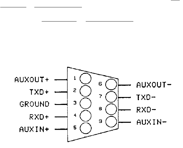
X. EXTERNAL CONNECTIONS
Connections to peripheral equipment are made via a
female D-9 connector. A pin-out of the D-9 connector
and a detailed description of each output signal is
illustrated in figures 24 and 25.
Figure 24. D-9 output configuration.
+-----+------------+----------------------------------+
| PIN | SIGNAL | DESCRIPTION |
+-----+------------+----------------------------------+
| 1 | AUX OUT+ | When combined with AUX OUT-, |
| | | provides the auxiliary channel |
| | | output defined by jumpers J2/J3. |
+-----+------------+----------------------------------+
| 2 | DATA OUT+ | When combined with DATA OUT-, |
| | | provides the serial data output. |
+-----+------------+----------------------------------+
| 3 | SIGNAL GND | |
+-----+------------+----------------------------------+
| 4 | DATA IN+ | When combined with DATA IN-, |
| | | provides the serial data input. |
+-----+------------+----------------------------------+
| 5 | AUX IN+ | When combined with AUX IN-, |
| | | provides the auxiliary channel |
| | | input defined by jumpers J2/J3. |
+-----+------------+----------------------------------+
| 6 | AUX OUT- | See AUX OUT+ |
+-----+------------+----------------------------------+
| 7 | DATA OUT- | See DATA OUT+ |
+-----+------------+----------------------------------+
| 8 | DATA IN- | See DATA IN+ |
+-----+------------+----------------------------------+
| 9 | AUX IN- | See AUX IN+ |
+-----+------------+----------------------------------+
Figure 25. D-9 signal definitions.
iii

INSTALLATION
XI. INSTALLATION
Make sure there is a copy of the
original reference diskette available.
This diskette must be modified to
accept any option adapters.
1. Turn unit off.
2. Remove system cover as instructed in the IBM
Quick Reference Guide.
3. Insert adapter into any vacant slot following the
guidelines for installing an optional adapter in
the IBM Quick Reference Guide.
4. Replace system cover.
5. Turn unit on and insert copy of reference
diskette into drive A.
6. Respond "N" to automatic configuration.
7. Select "Copy an option diskette" and follow
copying instructions.
8. Select "Set configuration"
9. Select "Change configuration" or "Run automatic
configuration" and follow instructions.
After the initial installation, the reference diskette
will contain the configuration file for the DS-2000.
Subsequent re-installation or address changes may omit
step 7 and a "Y" response may be given in step 6
(automatically configure system) if desired.
XII. SPECIFICATIONS
Bus interface: IBM MicroChannel 16-bit bus
Controllers: 2 - 16550 Asynchronous Communication
Elements (ACEs)
RS-422 interface: 2 - D-9 connectors (female)
Transmit drivers: MC3486 or compatible
Receive buffers: MC3487 or compatible
I/O Address range: See figure 17
Interrupt levels: IRQ 3,4,7,9
Power requirements:
+--------+--------+-----------+
| I T | I MS | Supply |
+--------+--------+-----------+
| 630mA | 720mA | +5 Volts |
| -- | -- | +12 Volts |
| -- | -- | -12 Volts |
+--------+--------+-----------+
I T - Typical adapter current
I MS - Maximum statistical adapter current
iii
