Icon Health and Fitness BMD1 BMD-ICN-1 User Manual BMD 200
Icon Health and Fitness, Inc. BMD-ICN-1 BMD 200
User Manual

BMD-ICN-1 Datasheet v1.0 CONFIDENTIAL Page 1 of 11
BMD-ICN-1 Module for Bluetooth 4.1 LE
Table of Contents
1. QUICK SPECIFICATIONS ................................................................................................................................................ 2
2. PIN DESCRIPTIONS ....................................................................................................................................................... 3
3. ELECTRICAL SPECIFICATIONS ........................................................................................................................................ 4
3.1. ABSOLUTE MAXIMUM RATINGS ............................................................................................................................ 4
3.2. OPERATING CONDITIONS....................................................................................................................................... 4
3.3. GENERAL PURPOSE I/O .......................................................................................................................................... 4
3.4. DEBUG & PROGRAMMING .................................................................................................................................... 5
3.5. CLOCKS .................................................................................................................................................................. 5
4. MECHANICAL DATA ...................................................................................................................................................... 6
4.1. MODULE DIMENSIONS .......................................................................................................................................... 6
4.2. RECOMMENDED PCB LAND PAD ............................................................................................................................ 6
5. MODULE MARKING ...................................................................................................................................................... 7
5.1. MECHANICAL ENCLOSURE ..................................................................................................................................... 7
6. REGULATORY STATEMENTS ......................................................................................................................................... 8
6.1. FCC STATEMENT: ................................................................................................................................................... 8
6.2. FCC IMPORTANT NOTES: ........................................................................................................................................ 8
6.3. IC STATEMENT: ...................................................................................................................................................... 9
6.4. IC IMPORTANT NOTES: ........................................................................................................................................ 10
6.5. CE REGULATORY: ................................................................................................................................................. 10
7. SOLDER REFLOW TEMPERATURE-TIME PROFILE ......................................................................................................... 11
BMD-ICN-1 Datasheet v1.0 CONFIDENTIAL Page 2 of 11
1. Quick Specifications
Bluetooth
Version
4.1 (Bluetooth Smart) Peripheral/Central (S130)
Security
AES-128
LE connections
up to 3 as Central, up to one a Peripheral (S130, simultaneous)
Radio
Frequency
2.402GHz to 2.480GHz
Modulations
GFSK at 250 kbps, 1 Mbps (BLE), 2 Mbps data rates
Transmit power
+4 dBm
Receiver sensitivity
-93 dBm (BLE mode)
Antenna
PCB Trace Antenna
Current Consumption
TX only @ +4 dBm, 0 dBm, -4 dBm
16 mA, 10.5 mA, 8 mA
RX only @ 2 Mbps, 1 Mbps, 250 kbps
13.4 mA, 13 mA, 12.6 mA
CPU @ 16MHz from flash, from RAM
4.4 mA, 2.4 mA
System Off , w/ 16K RAM, 8K RAM, no RAM retention
1.8 uA, 1.2 uA, 0.6 uA
Dimensions
Length
18.5mm
Width
13.25 mm
Height
2.0 mm
Hardware
Interface
SPI Master/Slave, UART, Two-Wire Master, GPIO
Power supply
1.8V to 3.6V
Temperature Range
-25 to +75°C
Certifications
FCC
FCC part 15 modular qualification – FCC ID: OMCBMD1
IC
Industry Canada RSS-210 modular qualification – IC: 3673A-BMD1
CE
EN 60950-1: 2011-01 3.1 (a) : Health and Safety of the User
EN 301 489-17 V2.2.1 3.1 (b) : Electromagnetic Compatibility
EN 300 328 V1.8.1 3.2 : Effective use of spectrum allocated
Bluetooth
End Product with S130 1.0.0 – DID: TBD
Table 1- Quick Specifications

BMD-ICN-1 Datasheet v1.0 CONFIDENTIAL Page 3 of 11
2. Pin Descriptions
Figure 1- Pin out (Top View)
Pin description
Name
Pin
Direction
Description
P0.21
7
In/Out
GPIO
P0.22
8
In/Out
GPIO
P0.23
9
In/Out
GPIO
P0.24
10
In/Out
GPIO
P0.25
11
In/Out
GPIO
P0.26
12
In/Out
GPIO
P0.27
13
In/Out
GPIO
P0.28
14
In/Out
GPIO
P0.29
15
In/Out
GPIO
P0.30
19
In/Out
GPIO
P0.00
20
In/Out
DTM UART RX
P0.01
21
In/Out
DTM UART TX
P0.02
22
In/Out
GPIO
P0.03
23
In/Out
GPIO
P0.04
24
In/Out
GPIO
P0.05
25
In/Out
GPIO
P0.06
26
In/Out
GPIO
P0.07
27
In/Out
GPIO
P0.08
28
In/Out
GPIO
P0.09
31
In/Out
GPIO
P0.10
32
In/Out
GPIO
P0.11
33
In/Out
GPIO
P0.12
34
In/Out
GPIO
P0.13
35
In/Out
GPIO
P0.14
36
In/Out
GPIO
P0.15
37
In/Out
GPIO
P0.16
38
In/Out
GPIO
SWDIO
39
In/Out
SWDIO/ RESET
̅
̅
̅
̅
̅
̅
̅
̅
̅
SWCLK
40
In
SW Clock
P0.17
41
In/Out
GPIO
P0.18
42
In/Out
GPIO
P0.19
43
In/Out
GPIO
P0.20
44
In/Out
GPIO
VCC
17
Pwr
+1.8 to +3.6VDC input
GND
1, 2, 3, 4, 5, 6, 16, 18,
29, 30, 45, 46, 47
Pwr
Electrical Ground
Table 2 – Pin Descriptions
Note 1: An external capacitor for VCC is not strictly required, however
using a 1µF - 4.7µF ceramic capacitor is recommended.
1
2
3
4
5
6
7
8
9
10
11
12
13
14
1516
17
18
19
20
21
22
23
24
25
26
27
28
29
30 31
32
33
34
35
36
37
38
39
40
41
42
43
44
45
46
47
BMD-ICN-1 Datasheet v1.0 CONFIDENTIAL Page 4 of 11
3. Electrical Specifications
3.1. Absolute Maximum Ratings
Symbol
Parameter
Min.
Max.
Unit
VCC_MAX
Voltage on supply pin
-0.3
3.9
V
VIO_MAX
Voltage on GPIO pins
-0.3
VCC + 0.3
V
TS
Storage Temperature Range
-40
125
°C
Table 3 – Absolute Maximum Ratings
3.2. Operating Conditions
Symbol
Parameter
Min.
Typ.
Max.
Unit
VCC
Operating supply voltage
1.8
3.0
3.6
V
TR_VCC
Supply rise time (0V to 1.8V)
-
-
60
ms
TA
Operating Ambient Temperature Range
-25
25
75
°C
TAext
Extended Operating Temperature Range 1
-25
25
85
°C
Note 1: VCC range reduced to 1.9V to 3.6V. Some degradation in RF performance. See Nordic
Semiconductor’s ‘nRF51822 specification for Industrial Temperature Range’ Addendum for full details (QFAC
variant).
Table 4 – Operating Conditions
3.3. General Purpose I/O
The general purpose I/O is organized as one port enabling access and control of the 31 available GPIO pins through
one port. Each GPIO can be accessed individually with the following user configurable features:
Input/output direction
Output drive strength
Internal pull-up and pull-down resistors
Wake-up from high or low level triggers on all pins
Trigger interrupt on all pins
All pins can be used by the PPI task/event system; the maximum number of pins that can be interfaced
through the PPI at the same time is limited by the number of GPIOTE channels
All pins can be individually configured to carry serial interface or quadrature demodulator signals
Symbol
Parameter
Min.
Typ.
Max.
Unit
VIH
Input High Voltage
0.7 x VCC
-
VCC
V
VIL
Input Low Voltage
VSS
-
0.3 x VCC
V
VOH
Output High Voltage
VCC – 0.3
-
VCC
V
VOL
Output Low Voltage
VSS
-
0.3
V
RPU
Pull-up Resistance
11
13
16
kΩ
RPD
Pull-down Resistance
11
13
16
kΩ
Table 5 - GPIO
Note: GPIO have a standard drive strength of 0.5 mA, and a high drive strength of 5 mA. Maximum number of high
drive strength pins is 3.
BMD-ICN-1 Datasheet v1.0 CONFIDENTIAL Page 5 of 11
3.4. Debug & Programming
The BMD-ICN-1 supports the two pin Serial Wire Debug (SWD) interface and allows for debugging of program
code. Breakpoints, single stepping, and instruction trace capture of code execution flow are part of this support.
3.5. Clocks
The BMD-ICN-1 module requires two clocks, a high frequency clock and a low frequency clock.
The high frequency clock is provided internally by a high-accuracy 16-MHz crystal as required by the nRF51822
for radio operation.
The low frequency clock can be provided internally by an RC oscillator or synthesized from the fast clock; or
externally by a 32.768 kHz crystal. An external crystal provides the lowest power consumption. The internal RC
oscillator is sufficient for BLE operation and most designs, unless more accurate time keeping is required.
32.768 kHz Crystal Specification Requirements
Symbol
Parameter
Typ.
Max.
Unit
fnom
Crystal frequency
32.768
-
kHz
Ftol,BLE
Frequency tolerance, Bluetooth low energy
applications.
±250
-
ppm
Cl
Load Capacitance
-
12.5
pF
Co
Shunt Capacitance
-
2
pF
Rs
Equivalent series resistance
50
80
kΩ
Cpin
Input Capacitance on XTAL1 & XTAL2
5
-
pF
Table 6 - 32.768 kHz Crystal
32.768 kHz Oscillator Comparison
Symbol
Parameter
Typ.
Max.
Unit
IX32k
Current for 32.768kHz Crystal Oscillator
0.4
1
uA
IRC32k
Current for 32.768kHz RC Oscillator
0.8
1.1
uA
ISYNT32k
Current for 32.768kHz Synthesized Oscillator
15
-
uA
FTOL,X32k
Frequency Tolerance, 32.768kHz Crystal Oscillator
-
±250
ppm
F TOL,RC32k
Frequency Tolerance, 32.768kHz RC Oscillator
±2
-
%
F TOL,SYNT32k
Frequency Tolerance, 32.768kHz Synthesized Oscillator
±34
-
ppm
Table 7 - 32.768 kHz Oscillator
Note: FTOL,X32k is max tolerance allowed for BLE applications. Actual tolerance depends on the
crystal used.
BMD-ICN-1 Datasheet v1.0 CONFIDENTIAL Page 6 of 11
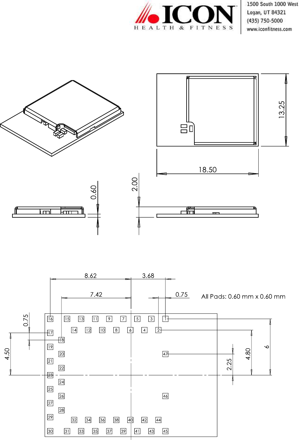
4. Mechanical Data
4.1. Module Dimensions
Figure 2- Module Dimensions
(All dimensions are in mm)
4.2. Recommended PCB Land Pad
Figure 3- Module Dimensions
BMD-ICN-1 Datasheet v1.0 CONFIDENTIAL Page 7 of 11
(All dimensions are in mm)
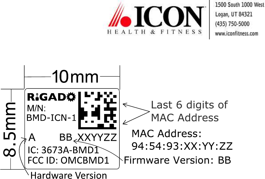
5. Module Marking
Figure 4 – Module Marking – Rev A – BMD-ICN-1-A (16kB)
Figure 5- Recommended RF Layout
5.1. Mechanical Enclosure
Care should be taken when designing and placing the module into an enclosure. Metal should be kept clear
from the antenna area, both above and below. Any metal around the module can negatively impact RF
performance.
The module is designed and tuned for the antenna and RF components to be in free air. Any potting, epoxy fill,
plastic overmolding, or conformal coating can negatively impact RF performance and must be evaluated by
the customer.

BMD-ICN-1 Datasheet v1.0 CONFIDENTIAL Page 8 of 11
6. Regulatory Statements
6.1. FCC Statement:
This device has been tested and found to comply with part 15 of the FCC rules. These limits are designed to
provide reasonable protection against harmful interference in a residential installation. This equipment
generates, uses and can radiate radio frequency energy and, if not installed and used in accordance with the
instructions, may cause harmful interference to radio communications. However, there is no guarantee that
interference will not occur in a particular installation. If this equipment does cause harmful interference to
radio or television reception, which can be determined by turning the equipment off and on, the user is
encouraged to try to correct the interference by one or more of the following measures:
Reorient or relocate the receiving antenna.
Increase the separation between the equipment and the receiver
Connect the equipment into an outlet on a circuit different from that to which the receiver is
connected.
Consult the dealer or an experienced radio/TV technician for help.
Operation is subjected to the following two conditions: (1) This device may no cause harmful interference, and
(2) this device must accept any interference received, including interference that may cause undesired
operation. Note: Modification to this product will void the user’s authority to operate this equipment.
Note: Modification to this product will void the users’ authority to operate this equipment.
6.2. FCC Important Notes:
(1) FCC Radiation Exposure Statement
This equipment complies with FCC RF radiation exposure limits set forth for an uncontrolled environment. This
transmitter must not be co-located or operating in conjunction with any other antenna or transmitter.
This equipment complies with Part 15 of the FCC Rules. Operation is subject the following two conditions:
(1) This device may not cause harmful interference, and
(2) This device must accept any interference received, including interference that may cause undesired
operation.
The devices must be installed and used in strict accordance with the manufacturer’s instructions as described
in the user documentation that comes with the product.
Caution!
The manufacturer is not responsible for any radio or TV interference caused by unauthorized modifications to
this equipment. Such modification could void the user authority to operate the equipment.
(2) Co-location Warning:
This device and its antenna(s) must not be co-located or operating in conjunction with any other antenna or
transmitter.
(3) OEM integration instructions:
This device is intended only for OEM integrators under the following conditions:
The antenna and transmitter must not be co-located with any other transmitter or antenna. The module shall

BMD-ICN-1 Datasheet v1.0 CONFIDENTIAL Page 9 of 11
be only used with the integral antenna(s) that has been originally tested and certified with this module.
As long as the two (2) conditions above are met, further transmitter testing will not be required. However, the
OEM integrator is still responsible for testing their end-product for any additional compliance requirements
with this module installed (for example, digital device emission, PC peripheral requirements, etc.)
In the event that these conditions cannot be met (for example certain laptop configuration or co-location with
another transmitter), then the FCC authorization for this module in combination with the host equipment is no
longer considered valid and the FCC ID of the module cannot be used on the final product. In these and
circumstance, the OEM integrator will be responsible for re-evaluating. The end product (including the
transmitter) and obtaining a separate FCC authorization.
Caution!
The OEM is still responsible for verifying compliance with FCC Part 15, subpart B limits for unintentional
radiators through a qualified test house.
(4) End product labeling:
The final end product must be labeled in a visible area with the following: “Contains FCC ID: OMCBMD1”.
Any similar wording that expresses the same meaning may be used.
The FCC Statement below should also be included on the label. When not possible, the FCC Statement should
be included in the User Manual of the host device.
“This device complies with part 15 of the FCC rules.
Operation is subject to the following two conditions. (1) This device may not cause harmful
interference. (2) This device must accept any interference received, including interference that may
cause undesired operation.”
(5) Information regarding the end user manual:
The OEM integrator has to be aware not to provide information to the end user regarding how to install or
remove this RF module in the user’s manual of the end product which integrates this module. The end user
manual shall include all required regulatory information/warning as show in this manual (Section 15.2(4)).
6.3. IC Statement:
This device complies with Industry Canada licence-exempt RSS standard(s). Operation is subject to the
following two conditions: (1) this device may not cause interference, and (2) this device must accept any
interference, including interference that may cause undesired operation of the device.
Le présent appareil est conforme aux CNR d'Industrie Canada applicables aux appareils radio exempts de
licence. L'exploitation est autorisée aux deux conditions suivantes : (1) l'appareil ne doit pas produire de
brouillage, et (2) l'utilisateur de l'appareil doit accepter tout brouillage radioélectrique subi, même si le
brouillage est susceptible d'en compromettre le fonctionnement.
RF exposure warning: The equipment complies with RF exposure limits set forth for an uncontrolled
environment. The antenna(s) used for this transmitter must not be co-located or operating in conjunction with
any other antenna or transmitter.
Avertissement d'exposition RF: L'équipement est conforme aux limites d'exposition aux RF établies pour un
incontrôlés environnement. L'antenne (s) utilisée pour ce transmetteur ne doit pas être co-localisés ou
onctionner en conjonction avec toute autre antenne ou transmetteur .

BMD-ICN-1 Datasheet v1.0 CONFIDENTIAL Page 10 of 11
6.4. IC Important Notes:
1. The OEM integrator has to be aware not to provide information to the end user regarding how to install or
remove this RF module in the user manual of the end product.
The user manual which is provided by OEM integrators for end users must include the following information in
a prominent location.
2. To comply with IC RF exposure compliance requirements, the antenna used for this transmitter must not be
co‐located or operating in conjunction with any other antenna or transmitter, except in accordance with IC
multi‐transmitter product procedures.
3. The final system integrator must ensure there is no instruction provided in the user manual or customer
documentation indicating how to install or remove the transmitter module except such device has
implemented two‐ways authentication between module and the host system.
4. The host device shall be properly labelled to identify the module within the host device. The final end
product must be labeled in a visible area with the following: “Contains IC: 3673A-BMD1”.
Any similar wording that expresses the same meaning may be used.
The IC Statement below should also be included on the label. When not possible, the IC Statement should be
included in the User Manual of the host device.
“This device complies with Industry Canada licence-exempt RSS standard(s). Operation is subject to
the following two conditions: (1) this device may not cause interference, and (2) this device must
accept any interference, including interference that may cause undesired operation of the device.
Le présent appareil est conforme aux CNR d'Industrie Canada applicables aux appareils radio exempts
de licence. L'exploitation est autorisée aux deux conditions suivantes : (1) l'appareil ne doit pas
produire de brouillage, et (2) l'utilisateur de l'appareil doit accepter tout brouillage radioélectrique
subi, même si le brouillage est susceptible d'en compromettre le onctionnement.”
6.5. CE Regulatory:
This device has been tested and have been found compliant against the following standards. OEM integrators
should consult with qualified test house to verify all regulatory requirements have been met for their
complete device.
From Directive 2006/95/EC:
EN 60950-1: 2006 + A11: 2009 + A1: 2010 + A12: 2011
From R&TTE Directive 1999/5/EC:
ETSI EN 300 440-1 V 1.6.1
ETSI EN 300 440-2 V 1.4.1
EN 62479:2010
From Directive 2004/108/EC:
ETSI EN 301 489-3 V1.6.1
ETSI EN 301 489-1 V1.9.2
BMD-ICN-1 Datasheet v1.0 CONFIDENTIAL Page 11 of 11
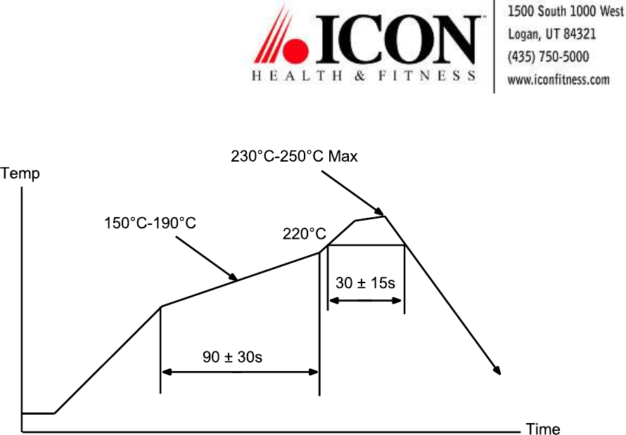
7. Solder Reflow Temperature-Time Profile
Figure 6 - Reflow Profile for Lead Free Solder