Impinj IPJRS500 Model IPJ-RS500GX 23 dBm RFID Reader SIP User Manual Title
Impinj, Inc. Model IPJ-RS500GX 23 dBm RFID Reader SIP Title
Impinj >
Users Manual
Hardware User’s Guide
www.impinj.com
Copyright © 2013, Impinj, Inc.
Impinj and Indy are either registered
trademarks or trademarks of Impinj, Inc.
For more information, contact readerchips@impinj.com
REV 0.3
Indy® RS500 Reader SiP: IPJ-RS500-GX and IPJ-
RS500-EU
Indy® RS500 Overview
Air Interface
Protocol
EPCglobal UHF Class 1 Gen 2 / ISO 18000-63 (formerly 18000-6C)
TX Output Power
13 to 23 dBm
Operating
Frequencies
IPJ-RS500-GX (902-928MHz) covers all 900MHz bands worldwide.
IPJ-RS500-EU (865-868MHz) covers current EU operating band.
Package size
29 mm x 32 mm x 3.8 mm
Package type
32-pin surface mount package (SMT compatible)
Rx sensitivity
-65dBm in DRM mode (1% packet error rate). Sensitivity will vary with antenna return loss.
High (good) return loss will yield better sensitivity while poor return loss will degrade sensitivity.
DC supply
3.6 to 5.25 volts
DC consumption
2.5 Watts typical at 23dBm output power
For technical support, visit the Impinj support portal at: support.impinj.com

Indy® RS500 Hardware User’s Guide
2 Revision 0.3, Copyright © 2013, Impinj, Inc.
TABLE OF CONTENTS
INTRODUCTION .................................................................................................................................................. 3
REGULATORY GUIDELINES ............................................................................................................................ 4
PRODUCT LABELLING............................................................................................................................................. 4
PRODUCT MANUALS .............................................................................................................................................. 5
US Requirements ............................................................................................................................................... 5
Canadian Requirements ..................................................................................................................................... 6
ANTENNA REQUIREMENTS ..................................................................................................................................... 6
MAXIMUM POWER EXPOSURE (MPE) AND USAGE LIMITATIONS ............................................................................. 7
RS500 SYSTEM BLOCK DIAGRAM .................................................................................................................. 8
PIN DESCRIPTIONS ............................................................................................................................................. 9
INTERFACING TO THE RS500 ........................................................................................................................ 10
OPERATING THE RS500 ................................................................................................................................... 12
RS500 DEVELOPMENT KIT ............................................................................................................................. 13
PACKAGE AND ASSEMBLY INFORMATION............................................................................................... 17
NOTICES: ............................................................................................................................................................. 20

Indy® RS500 Hardware User’s Guide
Revision 0.3, Copyright © 2013, Impinj, Inc. 3
Introduction
The Impinj® Indy®RS500 reader is a System-in-Package (SiP) that comprises a completely integrated solution for EPC Gen2 /
ISO18000-63 (formerly 18000-6C) applications. The SiP was developed to make embedding UHF RFID reader capability easy.
The Indy RS500 builds on market-leading Indy reader chip technology and integrates all of the necessary components into a tiny
package. It requires very few external components, is fully tested and is certified for modular operation under FCC and IC
regulations. The RS500 comes in a surface mount package designed to work as a SMT (surface mount technology) component in a
standard PCB manufacturing process.
This document provides instructions to the end-user to ensure optimal performance in their OEM hardware. Details on the use of
the Indy®RS500 Development Kit are also included to provide an example of appropriate application.

Indy® RS500 Hardware User’s Guide
4 Revision 0.3, Copyright © 2013, Impinj, Inc.
Regulatory Guidelines
The RS-500 (Impinj model number IPJ-RS500-GX) is approved for modular certification by FCC and Industry Canada (IC) under
the following ID numbers:
FCC ID: TWY-IPJRS500
IC: 6324A-IPJRS500
Modular approval allows installation in different end-use products by an original equipment manufacturer (OEM) with limited or
no additional testing or equipment authorization for the transmitter function provided by the RS500. Specifically:
No additional transmitter compliance testing is required if the module is operated with one of the antennas listed in the
document below.
No additional transmitter-compliance testing is required if the module is operated with the same general type of antenna
(i.e. near-field segmented loop, circularly polarized patches) as those listed in this User’s Guide and in the FCC filing for
the RS500. Acceptable antennas must be of equal or less far field gain than the antennas previously authorized under the
same FCC ID, and must have similar in band and out of band characteristics.
In addition, the end product must comply with all applicable FCC equipment authorizations, regulations, requirements and
equipment functions not associated with the RS500. For example, compliance must be demonstrated to regulations for other
transmitter components within the host product, to requirements for unintentional radiators (Part 15B), and to additional
authorization requirements for the non-transmitter functions.
The OEM applying the RS500 is required to include all FCC and/or IC statements and warnings detailed in the following sections
to the end product labelling (where specified) and in the finished product manual. The OEM must also strictly adhere to antenna
and installation guidelines and MPE restrictions stated in this document.
Product Labelling
A statement must be included on the exterior of the final OEM product which communicates that the device identified by the
aforementioned FCC and Industry Canada ID numbers are contained within the product. For example:
This product contains a radio module certified as FCC ID: TWY-IPJRS500 and IC: 6324A-IPJRS500
OR
Contains FCC ID: TWY-IPJRS500
Contains IC: 6324A-IPJRS500
The OEM must include the following statements on the exterior of the finished product unless the product is too small (e.g. less
than 4 x 4 inches):
This device complies with Part 15 of the FCC Rules. Operation is subject to the following two conditions: (1) this device may
not cause harmful interference, and (2) this device must accept any interference received, including any interference that may
cause undesired operation.

Indy® RS500 Hardware User’s Guide
Revision 0.3, Copyright © 2013, Impinj, Inc. 5
Product Manuals
The user manual for the end product must include the following information in a prominent location:
To comply with FCC’s RF radiation exposure requirements, the antenna(s) used for this transmitter must be installed such that
a minimum separation distance of 25cm is maintained between the radiator (antenna) & user’s/nearby people’s body at all
times and must not be co-located or operating in conjunction with any other antenna or transmitter
US Requirements
The finished product manual must contain the following statement:
WARNING: The Federal Communications Commission warns that changes or modifications of the radio module within this
device not expressly approved by Impinj, Inc. could void the user’s authority to operate the equipment.
In the case where an OEM seeks class B (residential) limits for the host product, the finished product manual must contain the
following statement:
Note: This equipment has been tested and found to comply with the limits for a Class B digital device, pursuant to part 15 of the
FCC Rules. These limits are designed to provide reasonable protection against harmful interference in a residential
installation. This equipment generates, uses and can radiate radio frequency energy and, if not installed and used in
accordance with the instructions, may cause harmful interference to radio communications. However, there is no guarantee
that interference will not occur in a particular installation. If this equipment does cause harmful interference to radio or
television reception, which can be determined by turning the equipment off and on, the user is encouraged to try to correct the
interference by one or more of the following measures:
Reorient or relocate the receiving antenna.
Increase the separation between the equipment and receiver.
Connect the equipment into an outlet on a circuit different from that to which the receiver is connected.
Consult the dealer or an experienced radio/TV technician for help.
In the case where an OEM seeks the lesser category of a Class A digital device for their finished product, the following statement
must be included in the manual of the finished product:
Note: This equipment has been tested and found to comply with the limits for a Class A digital device, pursuant to part 15 of the
FCC Rules. These limits are designed to provide reasonable protection against harmful interference when the equipment is
operated in a commercial environment. This equipment generates, uses, and can radiate radio frequency energy and, if not
installed and used in accordance with the instruction manual, may cause harmful interference to radio communications.
Operation of this equipment in a residential area is likely to cause harmful interference in which case the user will be required
to correct the interference at his expense.

Indy® RS500 Hardware User’s Guide
6 Revision 0.3, Copyright © 2013, Impinj, Inc.
Canadian Requirements
The OEM must include the following regulatory statements (shown in italics) in both English and French on the exterior of the
finished product and/or in the product manual:
This device complies with Industry Canada licence-exempt RSS standard(s). Operation is subject to the following two
conditions: (1) this device may not cause interference, and (2) this device must accept any interference, including interference
that may cause undesired operation of the device.
Le présent appareil est conforme aux CNR d'Industrie Canada applicables aux appareils radio exempts de licence.
L'exploitation est autorisée aux deux conditions suivantes : (1) l'appareil ne doit pas produire de brouillage, et (2) l'utilisateur
de l'appareil doit accepter tout brouillage radioélectrique subi, même si le brouillage est susceptible d'en compromettre le
fonctionnement.
The OEM must include the following regulatory statements (shown in italics) in both English and French in the finished product
manual:
Under Industry Canada regulations, this radio transmitter may only operate using an antenna of a type and maximum (or
lesser) gain approved for the transmitter by Industry Canada. To reduce potential radio interference to other users, the
antenna type and its gain should be so chosen that the equivalent isotropically radiated power (e.i.r.p.) is not more than that
necessary for successful communication.
This radio transmitter IC: 6324A-IPJRS500 has been approved by Industry Canada to operate with the antenna types listed
below with the maximum permissible gain and required antenna impedance for each antenna type indicated. Antenna types not
included in this list, having a gain greater than the maximum gain indicated for that type, are strictly prohibited for use with
this device.
Conformément à la réglementation d'Industrie Canada, le présent émetteur radio peut fonctionner avec une antenne d'un type
et d'un gain maximal (ou inférieur) approuvé pour l'émetteur par Industrie Canada. Dans le but de réduire les risques de
brouillage radioélectrique à l'intention des autres utilisateurs, il faut choisir le type d'antenne et son gain de sorte que la
puissance isotrope rayonnée équivalente (p.i.r.e.) ne dépasse pas l'intensité nécessaire à l'établissement d'une communication
satisfaisante.
Le présent émetteur radio IC: 6324A-IPJRS500 a été approuvé par Industrie Canada pour fonctionner avec les types d'antenne
énumérés ci-dessous et ayant un gain admissible maximal et l'impédance requise pour chaque type d'antenne. Les types
d'antenne non inclus dans cette liste, ou dont le gain est supérieur au gain maximal indiqué, sont strictement interdits pour
l'exploitation de l'émetteur.
Laird Technologies Model S9025-PR, CP patch antenna, 5.5dBi linear far field gain
Impinj, Inc. Mini-Guardrail Model IMP-A0303-00 Near Field antenna, -20 dBi far field gain
Antenna Requirements
In order to operate the RS500 under either FCC ID: TWY-IPJRS500 or IC: 6324A-IPJRS500, the OEM must strictly follow these
antenna guidelines:
The OEM may operate only with the following antennas or antenna types with maximum gain as shown :
o Laird Technologies Model S9025-PR, circularly-polarized patch antenna with 5.5dBi linear far field gain
o Impinj, Inc. Mini-Guardrail Model IMP-A0303-00, segmented loop (Near Field) antenna, -20 dBi far field gain

Indy® RS500 Hardware User’s Guide
Revision 0.3, Copyright © 2013, Impinj, Inc. 7
RF I/O interface to the antenna connector on the PCB shall be accomplished via a microstrip or stripline transmission line
with characteristic impedance of 50 ohms +/- 10%. A custom coaxial pigtail may also be utilized to connect to the
antenna in lieu of a connector.
The connector on the OEM’s PCB which interfaces to the antenna must be of a unique type to disable connection to a
non-permissible antenna in compliance with FCC section 15.203. The following connectors are allowed:
o Right angle Reverse-Polarity SMA (RP-SMA) Jack : Amphenol part number 132136RP or equivalent
o Ultra Miniature Coaxial Connector (UMCC) Jack: Molex part number 0734120110 or equivalent
o Custom 50 ohm coaxial pigtail from PCB to antenna
The OEM must professionally install the RS500 into its final environment to ensure that the conditions are met.
Maximum Power Exposure (MPE) and Usage Limitations
The minimum safe distance for people from the RS500 has been determined by conservative calculation to be less than 20 cm for
the allowable antenna types. The end product User’s Guide must include the following statement in a prominent location:
To comply with FCC’s RF radiation exposure requirements, the antenna(s) used for this transmitter must be installed such that
a minimum separation distance of 20 cm is maintained between the radiator (antenna) & user’s/nearby people’s body at all
times and must not be co-located or operating in conjunction with any other antenna or transmitter.
8 Revision 0.3, Copyright © 2013, Impinj, Inc.
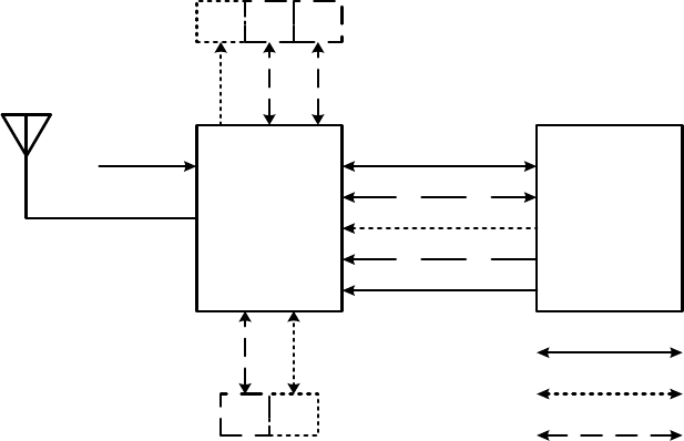
RS500 System Block Diagram
An example of a RS500 system-level block diagram for an embedded application is shown in Figure 1. Required connections are
illustrated with solid lines. Recommended and optional connections are illustrated with fine and coarse dotted lines, respectively.
Required connections:
VDC and GND are required to power the RS500.
RF pin must be connected to the OEM antenna.
UART1 provides host communications to control the operation of the RS500.
NRST pin resets the RS500 when set low.
Recommended connections:
BOOT0 provides a failsafe backdoor to the built-in bootloader of the RS500 microcontroller. If the Impinj
bootstrap is corrupted, the OEM may assert BOOT0 at reset to force the microcontroller to run its own internal
bootloader. The Impinj bootstrap and application can subsequently be reloaded.
UART2 provides debug information.
HEALTH indicates successful boot of the RS500. Connection to an LED provides a visual indication of
whether or not an error condition exists.
STATUS provides an indication when the RS500 is inventorying tags. Connection to an LED provides a visual
indicator of the tag activity.
Optional connections:
GPIO allow the user to trigger inventory, generate interrupts based on inventory activity, or provide general-
purpose user-controlled digital I/O
UC_ADC performs an analog-to-digital conversion of a 0 -3V input.
UC_DAC performs a digital-to-analog conversion of its digital input.
WKUP is a digital input which may wake the RS500 from its sleep mode, the lowest power state of the RS500.
RF
SWCLK
SWDIO
BOOT0
UART1 RX
UART1 TX
UC DAC
UC ADC
UART2 RX
UART2 TX
GPIO[3:2]
STATUS
HEALTH
RS500 Host
NRST
WKUP
VDC, GND
LEDs
Test
Point
Test
Point
User
Def.
User
Def.
GPIO[1:0]
REQUIRED
RECOMMENDED
OPTIONAL
Figure 1 - Example RS500 system

Revision 0.3, Copyright © 2013, Impinj, Inc. 9
Pin Descriptions
Pin #
Pin Name
Type+
Description
1
RFIO
RF In/Out
RF transmit/receive pin
2
GND
Power
Signal ground
3
SW_CLK
Digital input
JLink programmer/debugger clock line (Impinj use only)
4
SW_DIO
Digital I/O
JLink programmer/debugger data line (Impinj use only)
5
GND
Power
Signal ground
6
BOOT0
Digital input
Status at power-up determines microcontroller boot mode.
7
UART1-RX
Digital input
Host UART receive pin
8
UART1-TX
Digital output
Host UART transmit pin
9
nRST
Digital I/O
Holds RS500 in reset when low
10
GND
Power
Signal ground
11
VDC_IN
Power
DC supply voltage, 3.6V to 5.25V
12
WKUP
Digital input
Awakens RS500 from sleep mode
13
ADC
Analog input
Analog to digital converter input (future)
14
UART2-TX
Data
UART serial transmit pin
15
UART2-RX
Data
UART serial receive pin
16
DAC
Analog output
Digital to analog converter output (future)
17
GPIO1
Digital I/O
Configurable general purpose I/O
18
GPIO2
Digital I/O
Configurable general purpose I/O
19
GPIO3
Digital I/O
Configurable general purpose I/O
20
GPIO4
Digital I/O
Configurable general purpose I/O
21
Status
Digital output
Toggles between high and low state to indicate tag inventory
22
Health
Digital output
Toggles between high and low state to indicate RS500 ready
23-32
GND
Power
Signal ground
Table 1: RS500 Pinout
10 Revision 0.3, Copyright © 2013, Impinj, Inc.
Interfacing to the RS500
Power and Ground
All circuits on the RS500 are powered from a single input at pin 11. The RS500 operates with any supply voltage between 3.6 and
5.25V. Because the individual supplies within the part are regulated on the RS500, a large amount of supply filtering is not
required. A high value, low ESR tantalum capacitor (150uF or greater) is recommended and should be accompanied by a 0.1uF
ceramic chip capacitor close to the pin.
All 12 available ground pins of the RS500 must be soldered to the user PCB per the recommended assembly guidelines. If the PCB
utilizes separate analog/RF and digital grounds, it is recommended that the RS500 connect to the analog/RF ground. Providing a
highly conductive path from the SiP ground to a continuous ground plane (by use of numerous vias to the ground plane) and as
much ground conductor area as possible on the outer layers of the user PCB will help to reduce the RS500 temperature rise during
operation.
Communication
The RS500 has two UART ports, each of which utilizes 3.3V CMOS I/O over a pair of pins. The UARTs are compatible with a
standard RS-232C serial port through an appropriate level translator IC. The user’s host processor issues IRI commands to the
HOST UART (RX pin 7, TX pin 8), which can be configured for any standard UART data rate between 9.6 kbaud and 921.6
kbaud. The default rate is set to 115.2 kbaud. The DEBUG UART (RX pin 15, TX pin 14) is available to provide status
information from the RS500 microcontroller. The DEBUG UART is not required for RS500 reader applications and should be
operated at a fixed data rate of 115.2 kbaud. Please see the RS500 data sheet for detailed I/O specifications.
RF
The RS500 is configured for monostatic operation, which requires only a single RF I/O pin for full duplex communication. The
output must be routed to the antenna via 50 ohm microstrip or stripline on the OEM PCB. No coupling capacitor is required given
that the RF pin is AC-coupled internal to the RS500. To maximize the radiated power (and corresponding communication range),
the length of the transmission line between RS500 and antenna should be made as short as possible. Please refer to the Regulatory
Guidelines section for acceptable connectors and antenna types to ensure FCC and IC compliance in the USA and Canada. The
maximum output power of the RS500 is 23 dBm (200 mW).
GPIO
There are four user-configurable digital GPIOs on the RS500. The signals are number GPIO1 – GPIO4 and occupy pins 17 – 20
respectively. Each GPIO operates at standard 3.3V CMOS logic levels with a minimum output current capability of 8 mA per pin
while maintaining guaranteed noise margins. The pins can source/sink up to 20 mA with reduced/increased Vhigh or increased Vlow.
All I/O is rated to withstand a discharge of 2kV using the Human Body Model (HBM). Appropriate interface circuitry and layout
as well as handling of the OEM hardware should be applied. Please see the RS500 data sheet for detailed I/O specifications.
System Boot and Reset
The Impinj internal bootstrap is selected by default upon power-up of the RS500. The boot pin is held low by an internal 10KΩ
pulldown resistor to ground at the BOOT0 signal (pin 6). In the unlikely scenario that Flash becomes corrupted and the Impinj
bootstrap fails, the application of a logic high to the BOOT0 pin at power up will utilize the generic microcontroller bootloader that
is stored in read only memory. The generic boot mode should only be selected when the Impinj bootstrap fails.
Pin 9 of the RS500 comprises the NRST signal. The RS500 is held in reset if the signal is held low. The NRST signal is
bidirectional and is pulled up to 3.3V by ~50kΩ resistance internal to the RS500. Any external connection to this pin must
maintain a high impedance (>>50kΩ) other than when an external reset signal is applied. This allows the RS500 to exert control of
the reset line during power up and other situations that require it. An open drain type of connection and/or mechanical switch to
ground is recommended to facilitate external reset of the RS500.
Revision 0.3, Copyright © 2013, Impinj, Inc. 11
Health and Status
RS500 pin 22 is a dedicated digital output that indicates the HEALTH of the RS500. After the RS500 is successfully booted and
in its operational state, the health output switches between low and high logic states at a 1 Hz frequency. The OEM can digitally
monitor this signal or use it to drive an LED for visual indication of the RS500 health.
Pin 21 is a dedicated digital output that indicates the tag inventory STATUS of the RS500. When the RS500 is successfully
inventorying one or more tags the status output toggles between 1 and 0 at a 1 Hz rate. The output remains low when no tags are
being inventoried. Like the health signal, the OEM can monitor it via firmware or use it to drive an LED for visual indication to the
device user.
Auxiliary data converters
There is a pair of auxiliary data converters available on the RS500: a 12 bit digital to analog converter (DAC) and a 12 bit analog
digital converter (ADC). Each converter operates with a full scale range of 3.3V.
Microcontroller Debugger signals
Pins 3 and 4 on the RS500 are dedicated to the clock and data pins used by the internal microcontroller’s emulator/debugger. These
pins are used exclusively by the Impinj engineering team and are not required for OEM use.
12 Revision 0.3, Copyright © 2013, Impinj, Inc.
Operating the RS500
Once the required hardware connections are made to the RS500, the unit can be operated with simple software routines running on
the OEM’s host processor. The host software issues commands to configure the reader, set the reader’s idle mode and to start and
stop various Gen2 RFID reader operations. The required host commands are defined by the Impinj Radio Interface (IRI) API.
Please refer to the latest IRI release package for details on the definition and format of available commands.
An example of the sequence of events starting at reader power-up is:
1. Apply power to the RS500.
2. Establish an IRI connection to the device via the host software.
3. Configure the reader. Critical parameters are:
a. Region of operation
When configured for a specific region, the RS500 can operate only according to the air interface standards for that
region. Key communication parameters are not adjustable by the user but are inherent in the RS500 firmware. Please
see the latest IRI release package on the Impinj support portal for current information on supported regions. FCC/IC
regional operation is the default for the device.
NOTE: The OEM is strictly forbidden to operate the RS500 in a regional mode other than that in which the device is
located. Applicable agency certification must be obtained by the OEM for their product to operate in the region in
which it is located. The modular certification of the RS500 in the U.S. and Canada may only be utilized by OEM’s that
follow all guidelines set forth in this document.
b. RF output power
The RS500 output power must be set to a level between 10 and 23 dBm. The default power is set to the reader’s
maximum allowable of 23 dBm.
4. Initiate an RFID operation.
Gen2V2 RFID operations including Inventory, Read, Write, Lock and Kill are initiated with an IRI command. RFID operations
can be triggered through the use of RS500 GPIO lines or independently started in the OEM software.
5. Set the RS500 idle mode.
When the RS500 is not executing an RFID operation, it assumes a low power state until another RFID function is initiated by the
host. The RS500 idle modes vary from the lowest latency mode (Low Latency Idle) during which the reader draws 75 mA from a
5V supply to the lowest power mode (Sleep), which draws less than 100µA. Please see the IRI Release documentation and the
RS500 data sheet for detailed information about the relative power consumption in and recovery time from each of the RS500 idle
modes.
Revision 0.3, Copyright © 2013, Impinj, Inc. 13
RS500 Development Kit
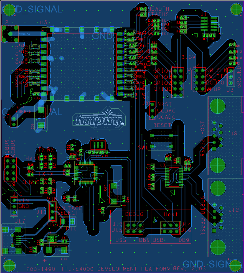
Impinj offers a Development Kit for the RS500 to provide a platform for OEM host software development as well as performance
evaluation of the RS500. The Development Kit PCBA demonstrates appropriate design and layout of required RS500 interfacing
circuitry in addition to visual indicators, test points and standard communication interfaces for ease of use.
Figure 2 – Development Kit PCB layout (top)

14 Revision 0.3, Copyright © 2013, Impinj, Inc.
The PCB comprises the following key interface elements:
Short, direct 50 ohm microstrip connecting RS500 RF I/O (U5, pin 1) to SMA connector
Jumper-selectable DC supply voltage
Connect a shorting plug between J11, pins 1 and 2 to select an external lab power source or between pins 2 and 3 to power the
RS500 from a USB interface at J17. The external DC supply is connected to J10, pin 1 (labelled ‘VIN’ on the PCB).
Jumper-selectable communications interface for host and debug UARTs
The development board houses both a USB-to-dual UART IC (U2) and a dual RS232-to-UART translator IC (U3), either of which
may be used to communicate to the RS500 UARTs. Shorting bars are used on headers J13 and J15 to set the HOST control source
and headers J14 and J16 to set DEBUG UART control source. Table 2 shows the configuration required for the various options.
Both headers of each pair must have jumpers properly installed for successful communication to take place.
Headers
Shorting bar position
UART control state
J13, J15
1-2
HOST controlled via RS-232 on DB9 connector J8
J13, J15
2-3
HOST controlled via USB
J14, J16
1-2
DEBUG controlled via RS-232 on DB9 connector J12
J14, J16
2-3
DEBUG controlled via USB
Table 2: UART control configuration
Indicator LEDs for all GPIOs, and Status and Health lines
Momentary pushbutton NRST switch
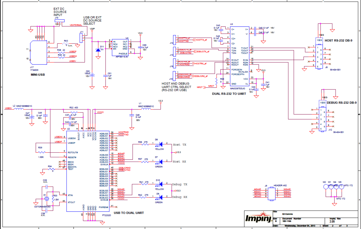
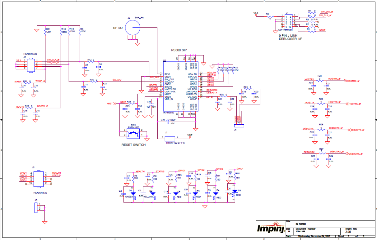
A complete schematic of the Development Kit PCBA is shown in Figure s 3 and 4.
Revision 0.3, Copyright © 2013, Impinj, Inc. 15
Figure 3 – Development Kit Schematic (1 of 2)
16 Revision 0.3, Copyright © 2013, Impinj, Inc.
Figure 4 – Development Kit Schematic (2 of 2)
Revision 0.3, Copyright © 2013, Impinj, Inc. 17
Package and Assembly Information
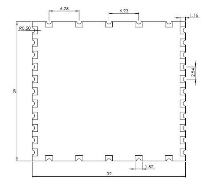
Figure 5 - Pin dimensions (units are in mm)
18 Revision 0.3, Copyright © 2013, Impinj, Inc.
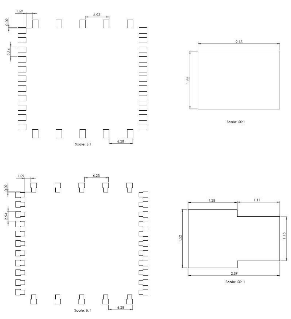
Figure 6 - Etched copper footprint and pad detail (units are in mm)
Figure 7 – Solder paste stencil pattern with single aperture detail (dimensions in mm)
Revision 0.3, Copyright © 2013, Impinj, Inc. 19
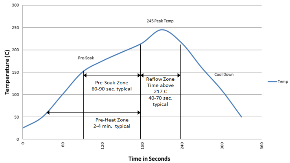
Figure 8 – Recommended Solder Reflow Profile
20 Revision 0.3, Copyright © 2013, Impinj, Inc.
Notices:
Copyright © 2013, Impinj, Inc. All rights reserved.
Impinj gives no representation or warranty, express or implied, for accuracy or reliability of
information in this document. Impinj reserves the right to change its products and services and
this information at any time without notice.
EXCEPT AS PROVIDED IN IMPINJ’S TERMS AND CONDITIONS OF SALE (OR AS
OTHERWISE AGREED IN A VALID WRITTEN INDIVIDUAL AGREEMENT WITH
IMPINJ), IMPINJ ASSUMES NO LIABILITY WHATSOEVER AND IMPINJ DISCLAIMS
ANY EXPRESS OR IMPLIED WARRANTY, RELATED TO SALE AND/OR USE OF IMPINJ
PRODUCTS INCLUDING LIABILITY OR WARRANTIES RELATING TO FITNESS FOR A
PARTICULAR PURPOSE, MERCHANTABILITY, OR INFRINGEMENT.
NO LICENSE, EXPRESS OR IMPLIED, BY ESTOPPEL OR OTHERWISE, TO ANY
PATENT, COPYRIGHT, MASK WORK RIGHT, OR OTHER INTELLECTUAL PROPERTY
RIGHT IS GRANTED BY THIS DOCUMENT.
Impinj assumes no liability for applications assistance or customer product design. Customers
should provide adequate design and operating safeguards to minimize risks.
Impinj products are not designed, warranted or authorized for use in any product or application
where a malfunction may reasonably be expected to cause personal injury or death or property or
environmental damage (“hazardous uses”) or for use in automotive environments. Customers
must indemnify Impinj against any damages arising out of the use of Impinj products in any
hazardous or automotive uses.
Indy is a trademark of Impinj, Inc. All other product or service names are trademarks of their
respective companies.
www.impinj.com