InVue ED0991 ED0991 UWB Module User Manual 15 3027 Manual
InVue Security ED0991 UWB Module 15 3027 Manual
InVue >
Manual

Model(s): ED0991 FCC ID: 2AFR8ED0991
ACS Project: 15-3027 Advanced Compliance Solutions Page 1
Certification Exhibit
FCC ID: 2AFR8ED0991
FCC Rule Part: Part 15.517
ACS Project Number: 15-3027
Manufacturer: InVue Security
Model: ED0991
Manual
ED0991 Module, Users Manual
Key Features
The ED0991 is a modular transceiver to meet the requirements of 47 C.F.R. § 15.212
(i) The radio elements of the ED0991 have their own shielding.
(ii) The ED0991 does not have modulation/data inputs. The modulation is generated internal and
the modulation type is fixed as BPM w/ BPSK. The data rates are fixed and set to the module via
an SPI interface to the host MCU.
(iii) The modular transmitter has its own power supply regulator.
An IEEE802.15.4-2011 UWB compliant wireless transceiver module based on DecaWave’s DW1000 IC.
Fully coherent receiver for maximum range and accuracy.
Designed to comply with FCC & ETSI UWB spectral masks
Supply voltage 2.8V to 3.6V
SPI Interface to host processor
Key Benefits
High immunity to multipath fading – allows reliable communications in high fading environments
Low power consumption allows operation from batteries for long periods*
Small physical size allows the implementation of cost-effective solutions in RTLS and WSN
Integrated antenna allows simple product implementation – no RF design required
Integration of DW1000 IC, antenna, power management and clock control simplifies design integration
Very precise location of tagged objects delivers enterprise efficiency gains and cost reductions
Long LOS and NLOS range reduces amount of infrastructure required to deploy systems
Low power consumption reduces the need to replace batteries and lowers system lifetime costs
Standards based solution (IEEE802.15.4-2011), eases proliferation
Low cost allows cost-effective implementation of solutions
The ED0991 module interfaces to an application microcontroller via SPI bus. Physical and MAC layer functionality
are accessed via the SPI bus, through addressable registers as well as execution commands. Data received or to be
transmitted are also accessed through the SPI bus and are implemented as a FIFO register (64 bytes each for TX
and RX). To transmit, a frame of data is placed in the FIFO, this may include a destination address. A transmit
command is given, which will transmit the data according to the initial setup of the registers. To receive data a
receive command is given, which will listen for a transmission and when one occurs put the received frame in the
FIFO. When neither transmit nor receive is required the device can enter either an Idle mode, from which it can
quickly re-enter receive or transmit mode or it can enter a low power sleep mode, from which a crystal startup is
also required prior to transmit or receive operation.
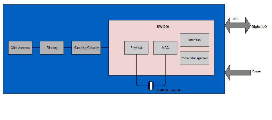
A block diagram is given for the ED0991 module in Figure 1.
Antenna
The antenna couples energy between the air and the module. The ED0991 module has an integrated antenna that
is near omni-directional. Note that the end radiation pattern depend not only on the antenna, but also the ground
plane, enclosure and installation environment.
Matching
The matching provides the correct loading of the transmit amplifier to achieve the highest output
power as well as the correct loading for the receive LNA to achieve the best sensitivity.
Physical
The physical layer provides conversions between data, symbol and RF signal.
MAC
The MAC layer is part of the Logical Link Layer and provides frame handling, addressing and
medium access services.
Microcontroller Interface
The microcontroller interface exposes registers and commands for the physical and MAC layers
to a microcontroller.
Power Management
Power management ensures a stable supply for the internal functions as well as providing means
for a low power sleep mode, in which most of the transceiver is power off.
Figure 1
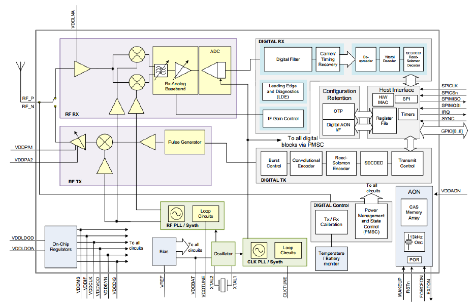
Typical Flow
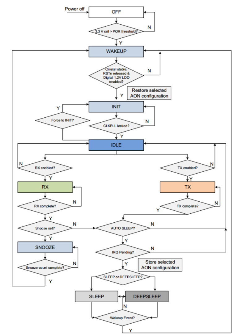
After initial setup of registers for desired behavior, the normal operation flow diagram is shown in. In applications
of infrequent data transmissions the transceiver would be in SLEEP mode to save power (<100nA). From there it
would be woken up and enter WAKEUP mode. As part of the wake up process the crystal oscillator is started
(~4ms) and the digital microcontroller interface is powered up. Before transmit or receive the frequency
synthesizer needs to be started RSTn and having been powered off (or idle for a while) the control loop of the
VCO/PLL needs to be calibrated INIT. A data frame is loaded into the transmit FIFO and the TX mode is entered. In
the TX state the DW1000 actively transmits a frame containing the contents of the transmit buffer on the
configured RF channel with the configured transmit parameters (PRF, data rate, preamble code etc.) Once the
frame transmission is complete the DW1000 may enter one of three modes depending on the programmed
configuration. After the frame transmission is complete the DW1000 will return to the IDLE state unless the
ATXSLP bit is set (in Sub-Register 0x36:04 – PMSC_CTRL1) in which case the DW1000 will enter the SLEEP or
DEEPSLEEP state automatically, (as long as no host interrupts are pending). When transmit is complete RX mode is
entered to either hunting for preamble or (once it has detected preamble) actively receiving preamble searching
for SFD, and subsequently receiving the PHR, decoding it and receiving the data part of the frame. In the RX state,
the RF synthesizer and all RX blocks are active. After an event that ends the reception, (either a good frame RX, or
some error or timeout event that aborts reception) the DW1000 will return to the IDLE state unless the ARXSLP bit
is set (in Sub-Register 0x36:04 – PMSC_CTRL1) in which case the DW1000 will enter the SLEEP or DEEPSLEEP state
automatically (as long as no host interrupts are pending).
Contents
Key Features .................................................................................................................................................. 1
Key Benefits ................................................................................................................................................... 1
Antenna ......................................................................................................................................................... 2
1. Overview ............................................................................................................................................... 5
1.1. ED0991 Functional Description ..................................................................................................... 6
1.2. ED0991 Power Up ......................................................................................................................... 6
1.3. SPI Host Interface .......................................................................................................................... 7
1.3.1. SPI Signal Timing ....................................................................................................................... 7
1.4. GPIO .............................................................................................................................................. 8
1.5. Always-On Memory (AON) ............................................................................................................ 9
1.6. One Time Programmable Memory ............................................................................................... 9
1.7. Interrupts and Device Status......................................................................................................... 9
1.8. MAC ............................................................................................................................................... 9
1.9. External Synchronization .............................................................................................................. 9
2. ED0991 Pin Connections ....................................................................................................................... 9
2.1. Pin Numbering ............................................................................................................................ 10
3.1. Nominal Operating Conditions ................................................................................................... 12
3.2. DC Characteristics ....................................................................................................................... 13
3.3. Receiver AC Characteristics ......................................................................................................... 13
3.4. Transmitter AC Characteristics ................................................................................................... 14
3.5. Temperature and Voltage Monitor ............................................................................................. 14
3.6. Antenna ....................................................................................................................................... 14
3.7. Absolute Maximum Ratings ........................................................................................................ 15
4. References .......................................................................................................................................... 15
5. Regulatory Approvals and Restrictions ............................................................................................... 15
1. Overview
The ED0991 module is an IEEE 802.15.4-2011 UWB implementation. RF components, Decawave DW1000 UWB
transceiver, and other components reside on-module. ED0991 enables cost effective and reduced complexity
integration of UWB communications and ranging features, greatly accelerating design implementation.
1.1. ED0991 Functional Description
The ED0991 on board the ED0991 is a fully integrated low-power, single chip CMOS RF transceiver IC compliant
with the IEEE 802.15.4-2011 [1] UWB standard.
The module contains an on-board 38.4 MHz reference crystal. The crystal has been trimmed in production to
reduce the initial frequency error to approximately 2 ppm, using the DW1000 IC’s internal on-chip crystal trimming
circuit, see section 2.1.1.
Always-On (AON) memory can be used to retain ED0991 configuration data during the lowest power operational
states when the on-chip voltage regulators are disabled. This data is uploaded and downloaded automatically. Use
of ED0991 AON memory is configurable.
The on-chip voltage and temperature monitors allow the host to read the voltage on the VDDAON pin and the
internal die temperature information from the DW1000.
See the DW1000 Datasheet [2] for more detailed information on device functionality, electrical specifications and
typical performance.
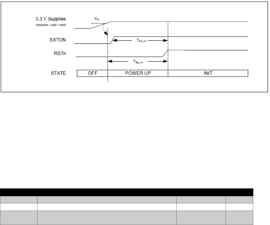
1.2. ED0991 Power Up
Figure 2:ED0991 Power up sequence
When power is applied to the ED0991, RSTn is driven low by internal circuitry as part of its power up sequence. See
Figure 2 above. RSTn remains low until the on-module crystal oscillator has powered up and its output is suitable
for use by the rest of the device, at which time RSTn is deasserted high.
Table 1: ED0991 Power up Timing
Parameter
Description
Nominal Value
Units
VON
Voltage threshold to enable power up
2.0
V
TEXT_ON
Time at which EXTON goes high before RSTn is released
3
msec
TDIG_ON
RSTn held low by internal reset circuit / driven low by
external reset circuit
3
msec
RSTn may be used as an output to reset external circuitry as part of system bring-up as power is applied.
An external circuit can reset the ED0991 by asserting RSTn for a minimum of 10 ns. RSTn is an asynchronous input.
ED0991 initialization will proceed when the pin is released to high impedance. RSTn should never be driven high by
an external source.
Please see DW1000 Datasheet [2] for more details of DW1000 power up.
1.3. SPI Host Interface
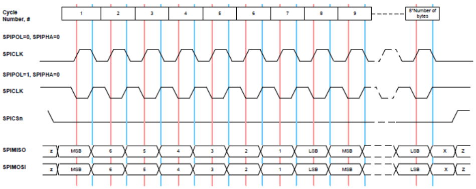
The DW1000 host communications interface is a slave-only SPI. Both clock polarities (SPIPOL=0/1) and
phases (SPIPHA=0/1) are supported. The data transfer protocol supports single and multiple byte
read/writes accesses.
All bytes are transferred MSB first and LSB last. A transfer is initiated by asserting
SPICSn low and terminated when SPICSn is deasserted high.
See the DW1000 Datasheet [2] for full details of the SPI interface operation and mode configuration for clock
phase and polarity.
Figure 3 ED0991 SPIPHA=0 TRANSFER PROTOCOL
1.3.1. SPI Signal Timing
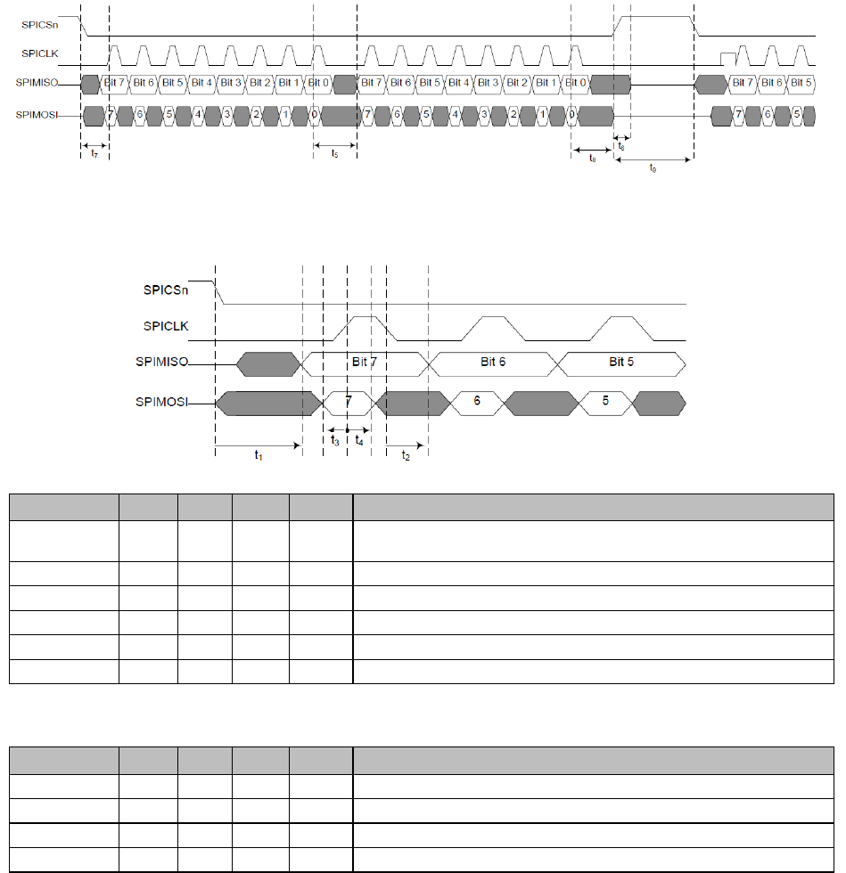
Figure 4 ED0991 Timing Diagram
Figure 5 ED0991 SPI Detailed Timing Diagram
Parameter
Min
Typ
Max
Unit
Description
SPICLK
Period
50
ns
The maximum SPI frequency is 20 MHz when the CLKPLL is locked,
otherwise the maximum SPI frequency is 3 MHz.
t1
38
ns
SPICSn select asserted low to valid slave output data
t2
12
ns
SPICLK low to valid slave output data
t3
10
ns
Master data setup time
t4
10
ns
Master data hold time
t5
32
ns
LSB last byte to MSB next byte
Parameter
Min
Typ
Max
Unit
Description
t6
10
ns
SPICSn de-asserted high to SPIMISO tri-state
t7
16
ns
Start time; time from select asserted to first SPICLK
t8
40
ns
Idle time between consecutive accesses
t9
40
ns
Last SPICLK to SPICSn de-asserted
1.4. GPIO
The ED0991 provides 8 configurable pins.
On reset, all GPIO pins default to input. GPIO inputs, when appropriately configured, are capable of
generating interrupts to the host processor via the IRQ signal.
GPIO0, 1, 2, & 3, as one of their optional functions, can drive LEDs to indicate the status of various chip
operations. Any GPIO line being used to drive an LED in this way should be connected as shown. GPIO5
& 6 are used to configure the operating mode of the SPI as described in the DW1000 Datasheet [2].
See DW1000 Datasheet [2] and DW1000 User Manual [3] provide full details of the configuration and
use of the GPIO lines.
1.5. Always-On Memory (AON)
Configuration retention in lowest power states is enabled in ED0991 by provision of an Always-On (AON)
memory array with a separate power supply, VDDAON. The ED0991 may be configured to upload its
configuration to AON before entering a low-power state and to download the configuration when
waking up from the low –power state.
1.6. One Time Programmable Memory
The ED0991 contains a 56x32 -bit user programmable OTP memory on the DW1000 device that is used
to store per chip calibration information.
1.7. Interrupts and Device Status
ED0991 has a number of interrupt events that can be configured to drive the IRQ output pin. The default
IRQ pin polarity is active high. A number of status registers are provided in the system to monitor and
report data of interest. See DW1000 User Manual [3] for a full description of system interrupts and their
configuration and of status registers.
1.8. MAC
A number of MAC features are implemented including CRC generation, CRC checking and receive frame
filtering. See the DW1000 Datasheet [2] and DW1000 User Manual [3] for full details
1.9. External Synchronization
The DW1000 provides a SYNC input. This allows: -
• Synchronization of multiple DW1000 timestamps
• Transmission synchronous to an external reference
• Receive time stamping synchronous to an external counter
See the DW1000 Datasheet [2] and DW1000 User Manual [3] for full details.
2. ED0991 Pin Connections
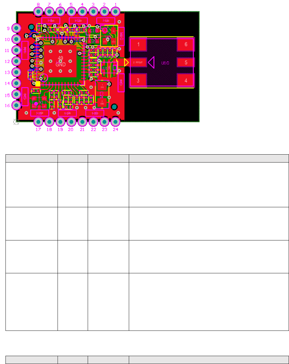
2.1. Pin Numbering
ED0991 module pin assignments are as follows (viewed from top): -
Table 2 ED0991 Pin Functions
Signal Name
PIN
I/O (Default)
Description
EXTON
1
O (O-L)
External device enable. Asserted during wake up process and
held active until device enters sleep mode. Can be used to
control external DC-DC converters or other circuits that are
not required when the device is in sleep mode so as to
minimize power consumption. Refer to DW1000 Datasheet
for more details [2].
WAKEUP
2
IO
When asserted into its active high state, the WAKEUP
pin brings the
DW1000 out of SLEEP or DEEPSLEEP states into
operational mode.
RSTn
3
IO(O-H)
Reset pin. Active Low Output.
May be pulled low by external open drain driver to
reset the DW1000. Refer to DW1000 Datasheet for
more details [2].
SYNC / GPIO7
4
IO(I)
The SYNC input pin is used for external synchronization
(Refer to
DW1000 Datasheet for more details [2]). When the
SYNC input
functionality is not being used this pin may be
reconfigured as a
general purpose I/O pin, GPIO7
Table 3 ED0991 Pin Functions Continued
Signal Name
PIN
I/O (Default)
Description

VDDA/ON
5
P
External supply for the Always-On (AON) portion of the
chip.
VDD
6,7
P
+3.3VDC supply pins
GND
8,16,21,
23,24
G
Common ground
GPIO6 / SPIPOL
9
IO(I)
General purpose I/O pin.
On power-up it acts as the SPIPOL (SPI polarity
selection) pin for configuring the SPI operation mode.
Refer to Section 4.2.2 and the DW1000 Datasheet for
more details [2].
After power-up, the pin will default to a General
Purpose I/O pin.
GPIO5 / SPIPHA
10
IO(I)
General purpose I/O pin.
On power-up it acts as the SPIPHA (SPI phase selection)
pin for configuring the SPI mode of operation. Refer to
Section 4.2.2 and the DW1000 Datasheet for more
details [2].
After power-up, the pin will default to a General
Purpose I/O pin.
GPIO4
11
IO(I)
General purpose I/O pin.
GPIO3 / TXLED
12
IO(I)
General purpose I/O pin.
It may be configured for use as a TXLED driving pin that
can be used to light a LED following a transmission.
Refer to the DW1000 User Manual [2] for details of LED
use.
GPIO2 / RXLED
13
IO(I)
General purpose I/O pin.
It may be configured for use as a RXLED driving pin that
can be used to light a LED during receive mode. Refer to
the DW1000 User Manual [2] for details of LED use.
GPIO1 / SFDLED
14
IO(I)
General purpose I/O pin.
It may be configured for use as a SFDLED driving pin
that can be used to light a LED when SFD (Start Frame
Delimiter) is found by the receiver. Refer to the
DW1000 User Manual [2] for details of LED use.
GPIO0 / RXOKLED
15
IO(I)
General purpose I/O pin.
It may be configured for use as a RXOKLED driving pin that can
be used to light a LED on reception of a good frame. Refer to
the DW1000 User Manual [2] for details of LED use.
SPICSn
17
I
SPI chip select. This is an active low enable input. The high-to-
low transition on SPICSn signals the start of a new SPI
transaction. SPICSn can also act as a wake-up signal to bring
DW1000 out of either SLEEP or DEEPSLEEP states Refer to
DW1000 Datasheet for more details [2].
SPIMOSI
18
I
SPI data input. Refer to DW1000 Datasheet for more details
[2].

Table 4 ED0991 Pin Functions Continued
Signal Name
PIN
I/O (Default)
Description
SPIMISO
19
O(O-L)
SPI data output. Refer to DW1000 Datasheet for more
details [2].
SPICLK
20
I
SPI clock
GNDIRQ / GPIO8
22
IO(O-L)
Common ground
GPIO6 / SPIPOL
9
IO(I)
Interrupt Request output from the ED0991 to the host
processor. By default IRQ is an active-high output but
may be configured to be active low if required. For
correct operation in SLEEP and DEEPSLEEP modes it
should be configured for active high operation. This pin
will float in SLEEP and DEEPSLEEP states and may cause
spurious interrupts unless pulled low.
When the IRQ functionality is not being used the pin
may be reconfigured as a general purpose I/O line,
GPIO8.
Table 5 Explanation of abbreviations
Abbreviation
Description
I
Input
I/O
Input/output
O
Output
G
Ground
P
Power Supply
PD
Power Decoupling
O-L
Defaults to output, low level after reset
O-H
Defaults to output, high level after reset
(I)
Defaults to input
Note: Any signal with the suffix ‘n’ indicates an active low signal.
3.1. Nominal Operating Conditions
Table 6 Normal Operating Conditions
Parameter
Min
Typ
Max
Units
Condition/Notes
Operating temperature
-40
+85
°C
Supply voltage VDDAON, VDD
2.8
3.3
3.6
V
Note: Unit operation is guaranteed by design when operating within these ranges

3.2. DC Characteristics
Tamb = 25 ˚C, all supplies centered on typical values
Table 7 DC Characteristics
Parameter
Min
Typ
Max
Units
Condition/Notes
Supply current DEEP SLEEP mode
200
nA
Total current drawn from all
supplies.
Supply current SLEEP mode
550
nA
Supply current IDLE mode
13.4
mA
Supply current INIT mode
3.5
mA
TX : 3.3 V supplies
(VDDAON, VDD)
mA
RX : 3.3 V supplies
(VDDAON, VDD)
mA
Digital input voltage high
V
Digital input voltage low
V
Digital output voltage high
V
Assumes 500 Ω load
Digital output voltage low
V
Digital Output Drive Current
GPIOx, IRQ
SPIMISO
EXTON
4
8
3
6
10
4
mA
Note: Unit operation is guaranteed by design when operating within these ranges
3.3. Receiver AC Characteristics
Tamb = 25 ˚C, all supplies centered on typical values
Table 8 Receiver Characteristics
Parameter
Min
Typ
Max
Units
Condition/Notes
Frequency range
3244
3993.6
6999
MHz
Must be set to 3993.6MHz
to comply with FCC/ETSI
certification.
Channel Bandwidth
500
MHz
Must be set to Channel 2
only to comply with
FCC/ETSI certification.
In-Band Blocking Level
30
dBc
Continuous Wave Interferer
Out-of--Band Blocking Level
55
dBc
Continuous Wave Interferer

3.4. Transmitter AC Characteristics
Tamb = 25 ˚C, all supplies centered on typical values
Table 9 Transmitter AC Characteristics
Parameter
Min
Typ
Max
Units
Condition/Notes
Frequency range
3244
3993.6
6999
MHz
Must be set to 3993.6MHz
to comply with FCC/ETSI
certification.
Channel Bandwidth
500
MHz
See DW1000 Datasheet [2]
Power Level Range
24
37
dB
Must be set to 24dB to
comply with FCC/ETSI
certification.
Coarse Power Level Step
3
dB
Fine Power Level Step
0.5
dB
Output power variation with
temperature
0.05
dB/°C
Output power variation with
voltage
2.73
dB/V
Channel 2
3.5. Temperature and Voltage Monitor
Tamb = 25 ˚C, all supplies centered on typical values
Table 10 Temperature and Voltage Monitor
Parameter
Min
Typ
Max
Units
Condition/Notes
Voltage Monitor Range
2.4
3.75
V
Voltage Monitor Precision
20
mV
Voltage Monitor Accuracy
140
mV
Temperature Monitor Range
-40
+100
°C
Temperature Monitor Precision
0.9
°C
3.6. Antenna
The antenna used in the module is the Partron dielectric chip antenna, part number ACS5200HFAUWB,
see [4] for full detail

3.7. Absolute Maximum Ratings
Table 11 Absolute Maximum Ratings
Parameter
Min
Max
Units
Voltage VDD/VDDAON
-0.3
4
V
Receive Power
0
dBm
Temperature – Storage
-40
+85
°C
Temperature – Operating
0
+40
°C
ESD (HBM)
2000
V
Stresses beyond those listed in this table may cause permanent damage to the device. This is a stress rating only;
functional operation of the device at these or any other conditions beyond those indicated in the operating
conditions of the specification is not implied. Exposure to the absolute maximum rating conditions for extended
periods may affect device reliability.
4. References
[1] IEEE802.15.4-2011 or “IEEE Std 802.15.4™‐2011” (Revision of IEEE Std 802.15.4-2006). IEEE Standard for Local
and metropolitan area networks - Part 15.4: Low-Rate Wireless Personal Area Networks (LR-WPANs). IEEE
Computer Society Sponsored by the LAN/MAN Standards Committee. Available from http://standards.ieee.org/
[2] Decawave DW1000 Datasheet www.decawave.com
[3] Decawave DW1000 User Manual www.decawave.com
[4] Partron Dielectric Chip Antenna, P/N ACS5200HFAUWB, www.partron.co.kr
5. Regulatory Approvals and Restrictions
The ED0991, as supplied from Invue Inc. and used only by Invue Inc. The module has been certified for use in the
United States and the European Union by the appropriate regulatory body governing radio emissions in that
region.
This equipment may only be operated indoors. Operation outdoors is in violation of 47 U.S.C. 301 and could
subject the operator to serious legal penalties.
The ED0991 module is based on DecaWave's DW1000 Ultra Wideband (UWB) transceiver IC. It contains an
integrated antenna, all RF circuitry, power management and clock circuitry in one module. All components with
the exception of the antenna are contained in a Steel Plated Tin shield with a thickness of 0.2mm. It can be used in
2-way ranging or TDOA location systems to locate assets to a precision of 10 cm.
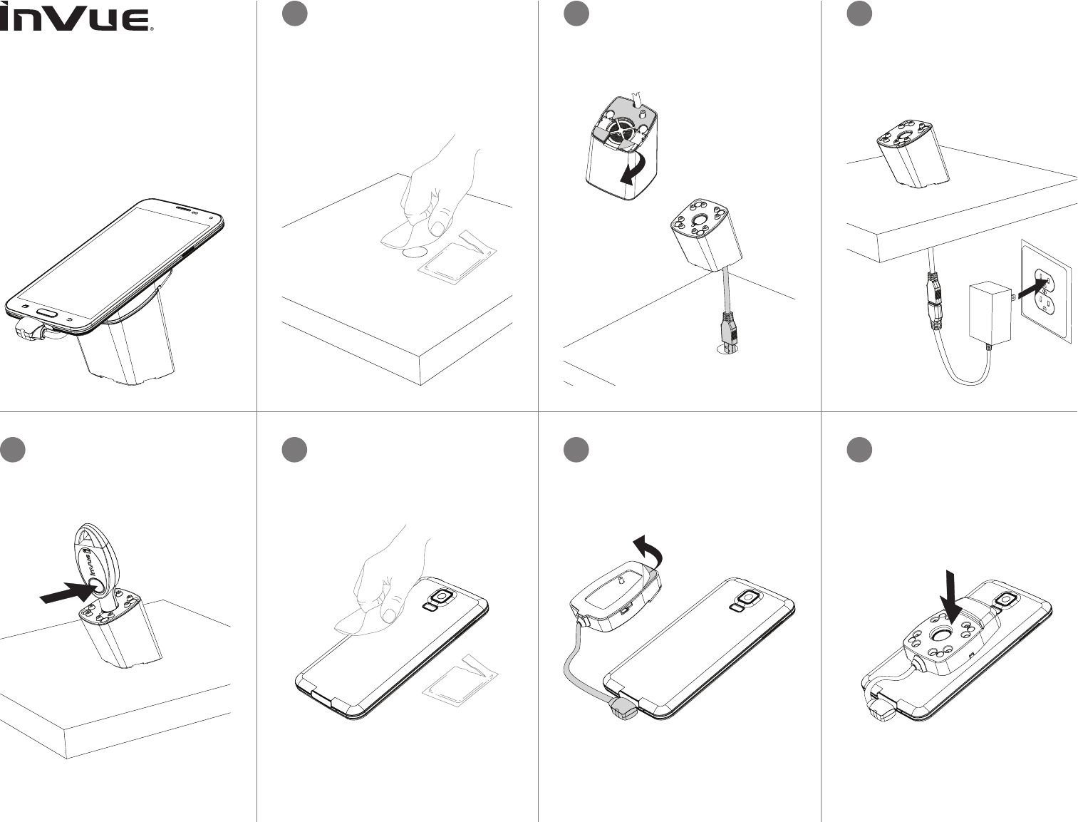
Wireless AP
Base & Sensor
Wipe xture with alcohol wipe
provided. Let it dry completely.
Optional: Drill a 22mm hole in
fixture.
1 2 Remove lm from all 3 adhesives
on bottom of base and slide base
cord through xture. Optional: Run
cord through back of stand along
fixture.
CONTENTS: One pad saturated in 75%
Isopropyl Alcohol
DIRECTIONS: Apply topically as
needed to cleanse surface mounting area.
FOR EXTERNAL USE ONLY
KEEP OUT OF REACH OF
CHILDREN
KEEP AWAY FROM EYES
AND FIRE
3Firmly press base onto xture for
10 seconds. Plug power supply into
base cord and outlet.
4Place IR2 key onto IR lens on base
and press button on IR2 key once to
transfer code into base.
Wipe back of merchandise with
alcohol wipe provided. Let it dry
completely.
Plug power connector into
merchandise and remove clear
lm from adhesive on sensor.
Center sensor onto back of
merchandise. Firmly press
sensor for 10 seconds.
5 6 7
CONTENTS: One pad saturated in 75%
Isopropyl Alcohol
DIRECTIONS: Apply topically as
needed to cleanse surface mounting area.
FOR EXTERNAL USE ONLY
KEEP OUT OF REACH OF
CHILDREN
KEEP AWAY FROM EYES
AND FIRE

Place sensor onto base to transfer
code onto sensor. Base and sensor
are now synched to each other only.
7
© 2015 InVue Security Products Inc. All rights reserved.
InVue is a registered trademark of InVue Security Products.
SD0278 Rev1 08/27/15
www.invuesecurity.com
NA / LATAM // 704.752.6513 • 888.55.INVUE
EMEA // +31.23.8900150
APAC // +852.3127.6811
Contains Module FCC ID: 2AFR8ED0991
THIS DEVICE COMPLIES WITH PART 15 OF
THE FCC RULES. OPERATION IS SUBJECT
TO THE FOLLOWING TWO CONDITIONS.
(1) THIS DEVICE MAY NOT CAUSE
HARMFUL INTERFERENCE, AND
(2) THIS DEVICE MUST ACCEPT ANY
INTERFERENCE RECEIVED,
INCLUDING INTERFERENCE THAT MAY
CAUSE UNDESIRED OPERATION.
Warning: Changes or modications to this
device not expressly approved by InVue
Security could void the user’s authority to
operate the equipment.
NOTE: This equipment has been tested and found
to comply with the limits for a Class B digital
device, pursuant to Part 15 of the FCC Rules.
These limits are designed to provide reasonable
protection against harmful interference in a
residential installation. This equipment generates,
uses, and can radiate radio frequency energy
and, if not installed and used in accordance with
the instructions, may cause harmful interference
to radio communications. However, there is no
guarantee that interference will not occur in a
particular installation. If this equipment does cause
harmful interference to radio or television reception,
which can be determined by turning the equipment
off and on, the user is encouraged to try to correct
the interference by one or more of
the following measures:
• Reorient or relocate the receiving antenna.
• Increase the separation between the equipment
and receiver.
• Connect the equipment into an outlet on a
circuit different from that to which the receiver is
connected.
• Consult the dealer or an experienced radio/TV
technician for help.
This equipment complies with FCC radiation
exposure limits set forth for an uncontrolled
environment. This equipment should be installed
and operated with minimum distance 20cm
between the radiator and your body. This
transmitter must not be co-located or operating in
conjunction with any other antenna or transmitter.