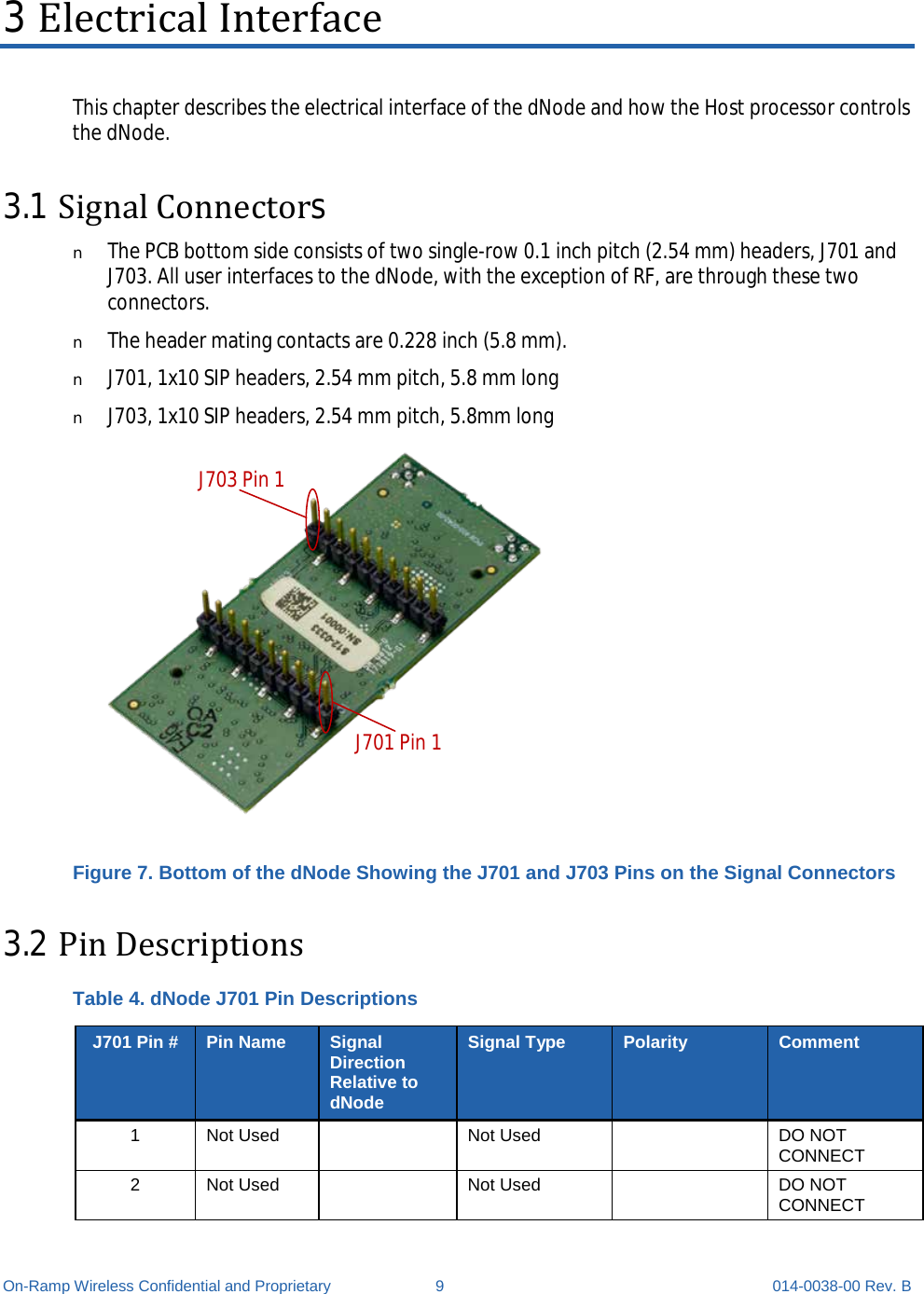
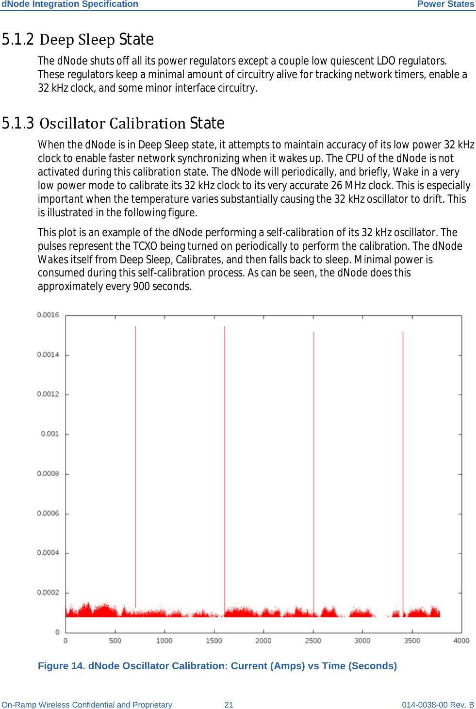
Ingenu ULPD100 The ULP dNode is a wireless network module User Manual dNode Integration Specification
On-Ramp Wireless The ULP dNode is a wireless network module dNode Integration Specification
UserManual.wiki
>
Ingenu
>
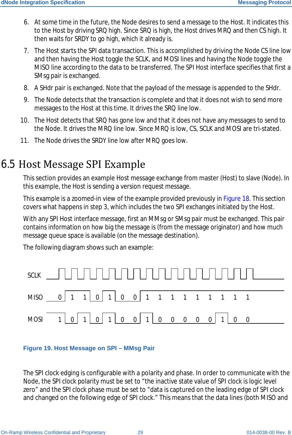
ULPD100 User Manual
User Manual
Navigation menu
Upload a User Manual
Namespaces
Wiki Guide
HTML
PDF
Info
Views
User Manual
Discussion / Help
Navigation
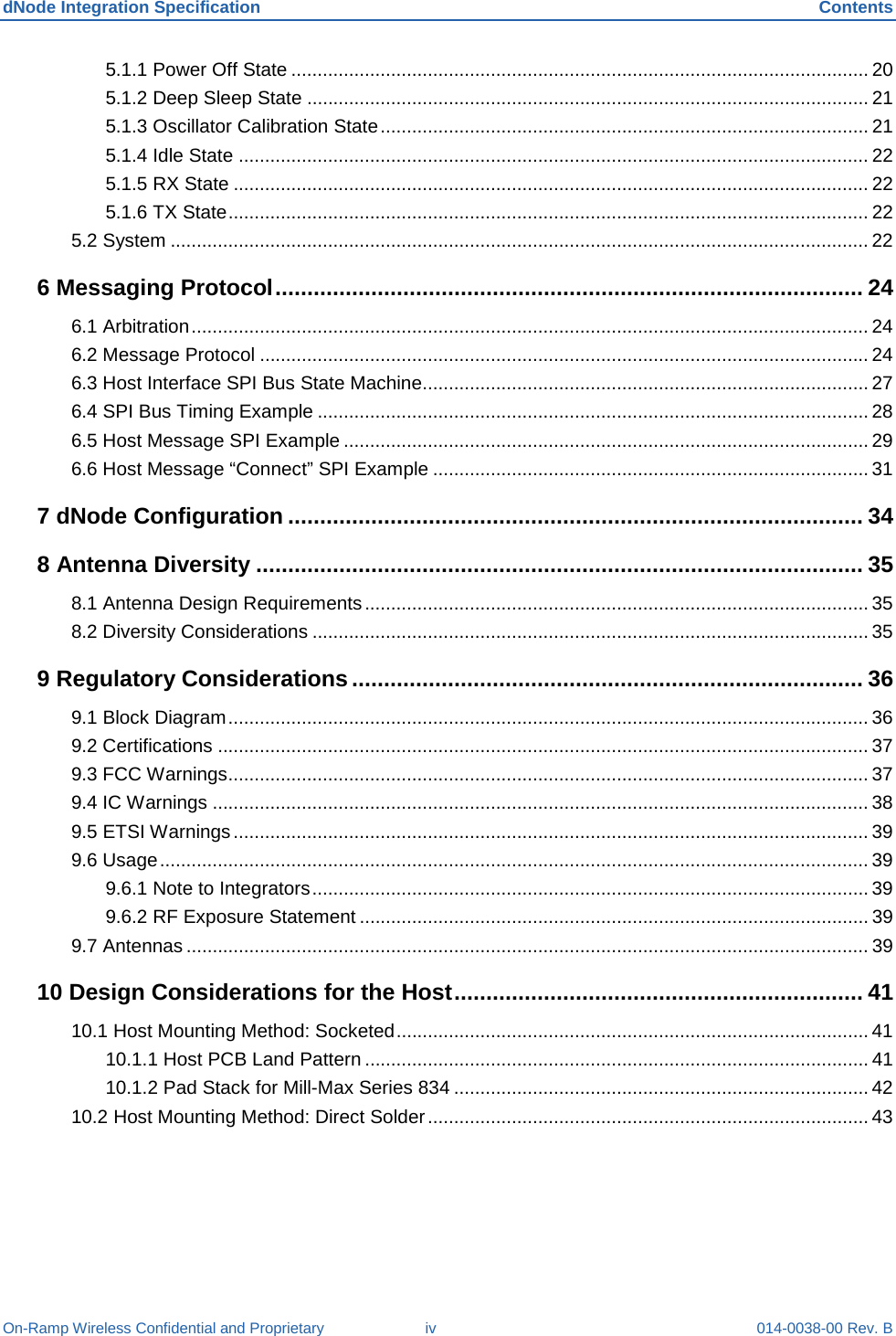
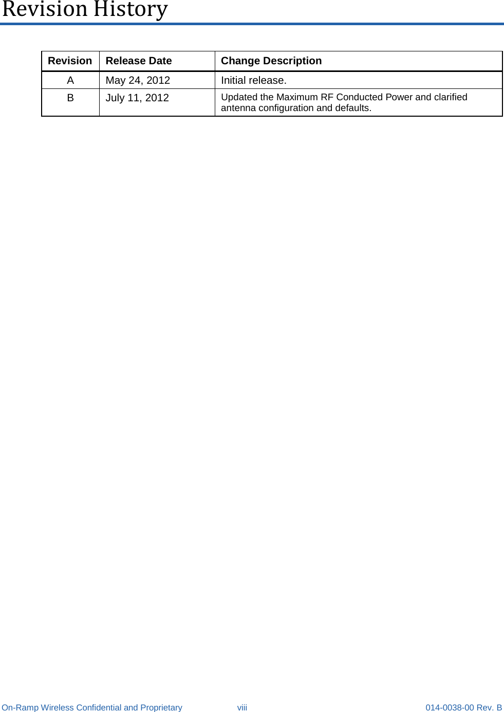
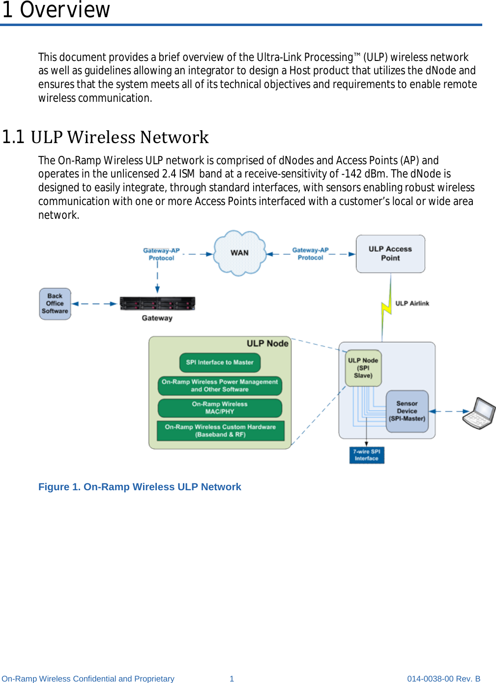
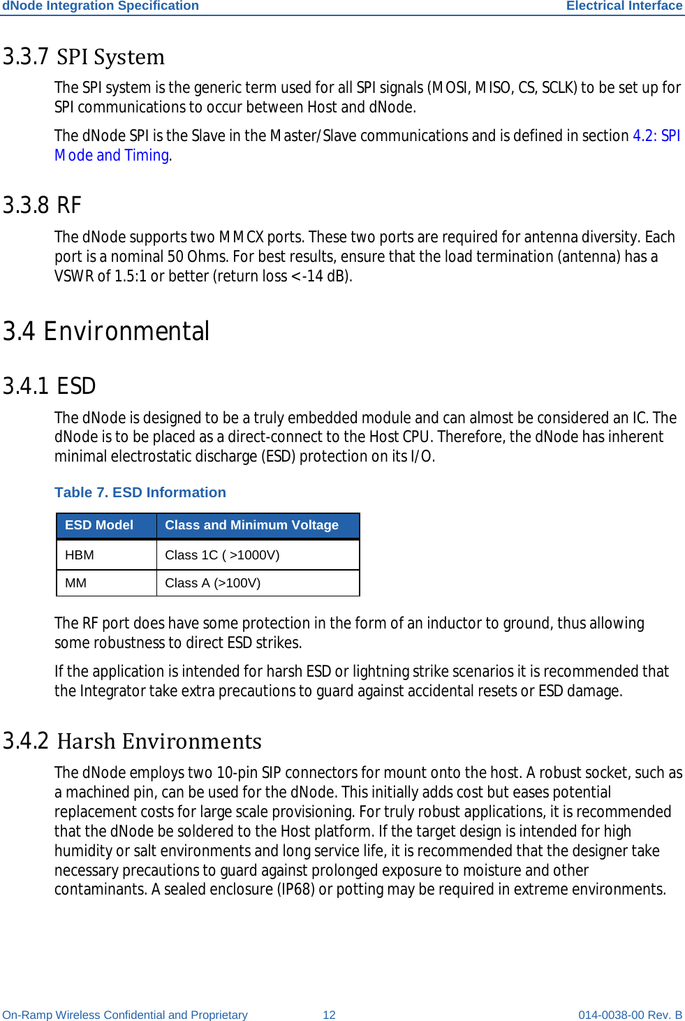
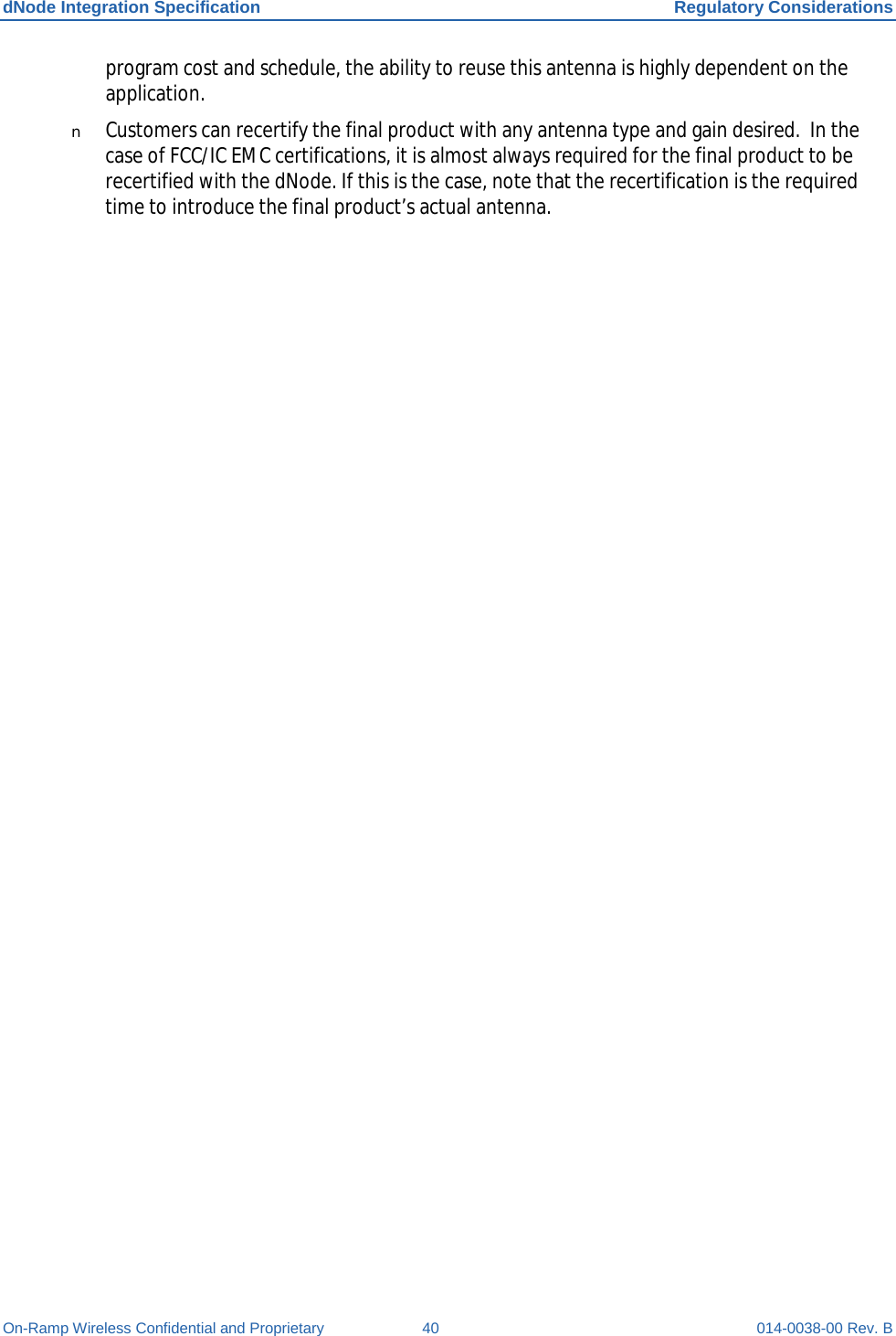
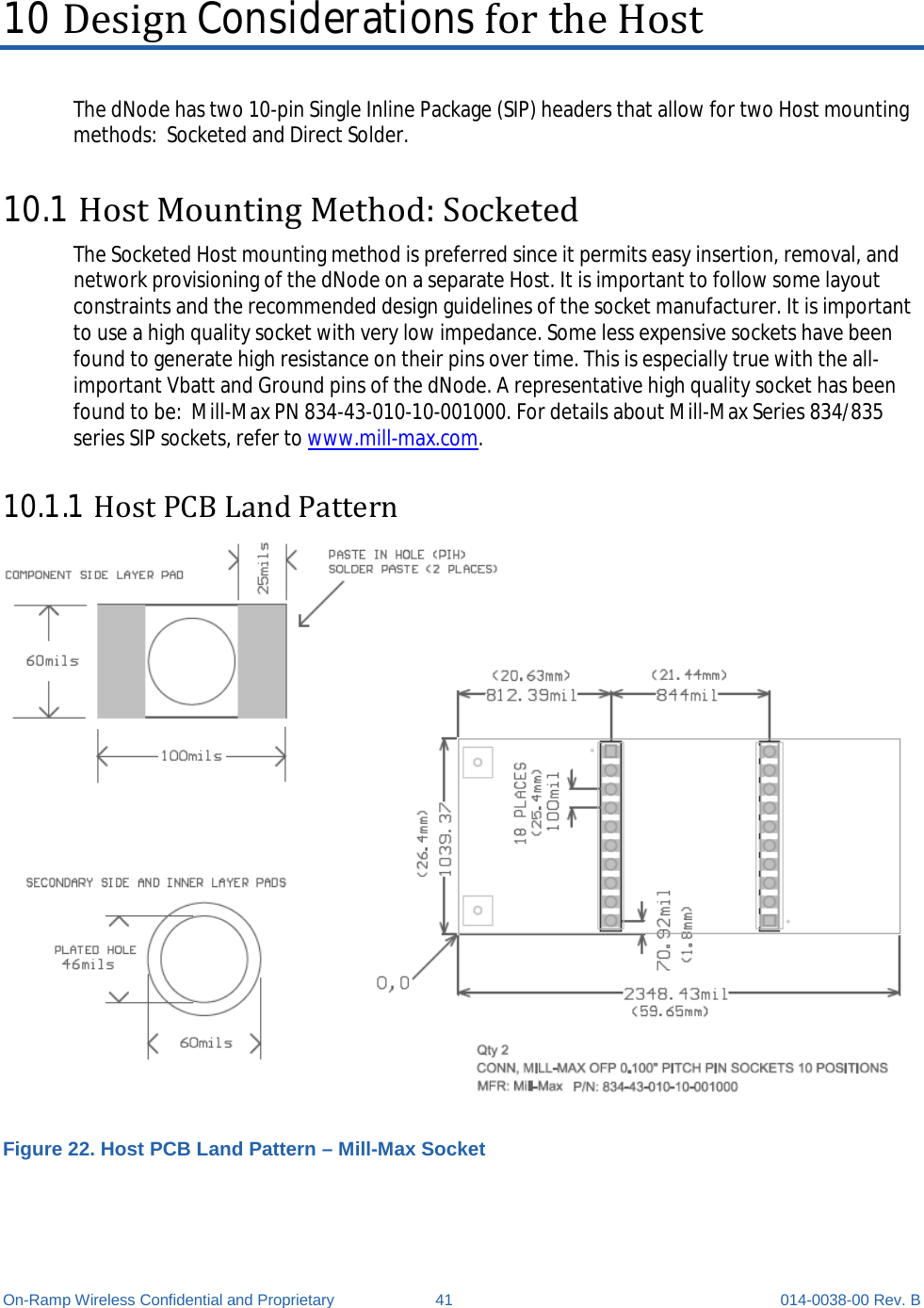
![dNode Integration Specification Design Considerations for the Host On-Ramp Wireless Confidential and Proprietary 43 014-0038-00 Rev. B 10.2 Host Mounting Method: Direct Solder The Direct Solder method of mounting the dNode gives little flexibility in insertion/removal but is the least expensive and can provide Low resistance on the Vbatt/Ground paths. PCB layout considerations are provided below. .100 [2.54] (TYP).844 [21.44] (TYP).040 [1.02] DIA (TYP) x20Optional square pads to indicate Pin 1 of connectors. Same drill diameter.Optional square pads to indicate Pin 1 of connectors. Same drill diameter.OptionalStencil Marks Figure 24. Host PCB Land Pattern – Direct Solder](https://usermanual.wiki/Ingenu/ULPD100/User-Guide-1787909-Page-51.png)