InnoComm Mobile Technology BM20 Wireless Module User Manual
InnoComm Mobile Technology Corporation Wireless Module
User Manual

BM20 BLE Single Mode Module
Product Specification
Model Name
BM20
Project code
Description
BLE Single Mode Module
Revision
1.0
Issue Date
2018/05/29
Approved by
Reviewed by
Issued by
Taka Wei
JH Huang
Iestyn Chen

BM20 Module Product Specification
05/31/2018
REV 1.0
Revision History
Revision Released Date Comments/Remark Author
0.1 2018/01/30 Initial release Iestyn Chen
0.2 2018/02/02 Update Block diagram, pin map and ME drawing Iestyn Chen
0.3 2018/02/23 Add reference circuit and Module Layout Guide Iestyn Chen
0.4 2018/03/31 Update Pin define and IO mapping table JH
0.5
2018/04/12
Modify the introduction
、
Block diagram and
Mechanical information
JH
1.0
2018/05/31
Modify specification
JH
® 2018 InnoComm Mobile Technology Corp.
Disclaimer
BM20 BLE MODULE are supplied “as is” and without warranties of any kind, express, implied, or statutory including,
but not limited to, any implied warranty for a particular purpose. No license is granted by implication or otherwise
under any patents or other intellectual property by application or use of evaluation boards. Information furnished by
InnoComm is believed to be accurate and reliable. InnoComm reserves the right to change specifications or product
description in this document at any time without notice.
Should Buyer purchase or use InnoComm’s products for any such unintended or unauthorized application, Buyer shall
indemnify and hold InnoComm harmless against all claims and damages.
InnoComm is the trademarks of InnoComm Mobile Technology Corp.
Other trademarks and registered trademarks mentioned herein are the property of their respective owners.
2/14
InnoComm Mobile Technology

BM20 Module Product Specification
05/31/2018
REV 1.0
3/14
InnoComm Mobile Technology
TABLE OF CONTENT
1.
INTRODUCTION ...................................................................................... 4
2.
GENERAL INFORMATION ................................................................... 5
3.
PIN MAP AND SIGNAL DESCRIPTION ............................................... 7
4.
ELECTRICAL CHARACTERISTICS ........................................................ 9
5.
RF CHARACTERISTICS .....................................................................10
6.
MECHANICAL INFORMATION ........................................................... 11
7.
PCB LAYOUT RECOMMENDATION ................................................. 11
8.
MODULE LAYOUT GUIDE ....................................................................12
9.
SMT SOLDER REFLOW RECOMMENDATION .................................... 14
10.
APPENDIX .............................................................................................. 15

BM20 Module Product Specification
05/31/2018
REV 1.0
4/14
InnoComm Mobile Technology
1.
INTRODUCTION
The Innocomm’s BM20 module based on Nordic’s outstanding nRF52832 BLE. It features a powerful CPU (ARM Cortex-
M4) and completes a lineup of Nordic’s Bluetooth 5 ready devices that together offer the full spectrum of possibilities
when designing Bluetooth® 5 into your products.
The BM20 supports key Bluetooth 5 features of high throughput (2Mbps) and increased broadcast capacity with
advertising extensions (x 8), as an optimized solution that makes it attractive in a very wide range of applications from
a performance.

BM20 Module Product Specification
05/31/2018
REV 1.0
5/14
InnoComm Mobile Technology
2.
General Information
2.1
Key Features
RF
•
2.4 GHz transceiver
•
-96 dBm sensitivity in Bluetooth® low energy mode
•
Supported data rates: 1 Mbps, 2 Mbps Bluetooth® low energy mode
•
-20 to +5 dBm TX power, configurable in 4 dB steps
•
RSSI (1 dB resolution)
•
ARM® Cortex®-M4 32-bit processor, 64 MHz
•
144 EEMBC CoreMark® score running from flash memory
•
34.4 μA/MHz running from flash memory
•
32.8 μA/MHz running from RAM
•
Serial wire debug (SWD)
•
Flexible power management
•
1.7 V-3.6 V supply voltage range
•
Fast wake-up using 64 MHz internal oscillator
•
512 kB flash and 64 kB RAM
•
Nordic SoftDevice ready
•
Support for concurrent multi-protocol
•
12-bit, 200 ksps ADC - 8 configurable channels with programmable gain
•
Temperature sensor
•
4-channel pulse width modulator (PWM) unit with EasyDMA
•
Digital microphone interface (PDM)
•
3x 32-bit timer with counter mode
•
SPI master/slave with EasyDMA
•
I2C compatible 2-wire master/slave
•
UART (CTS/RTS) with EasyDMA
•
Programmable peripheral interconnect (PPI)
•
Quadrature decoder (QDEC)
•
AES HW encryption with EasyDMA
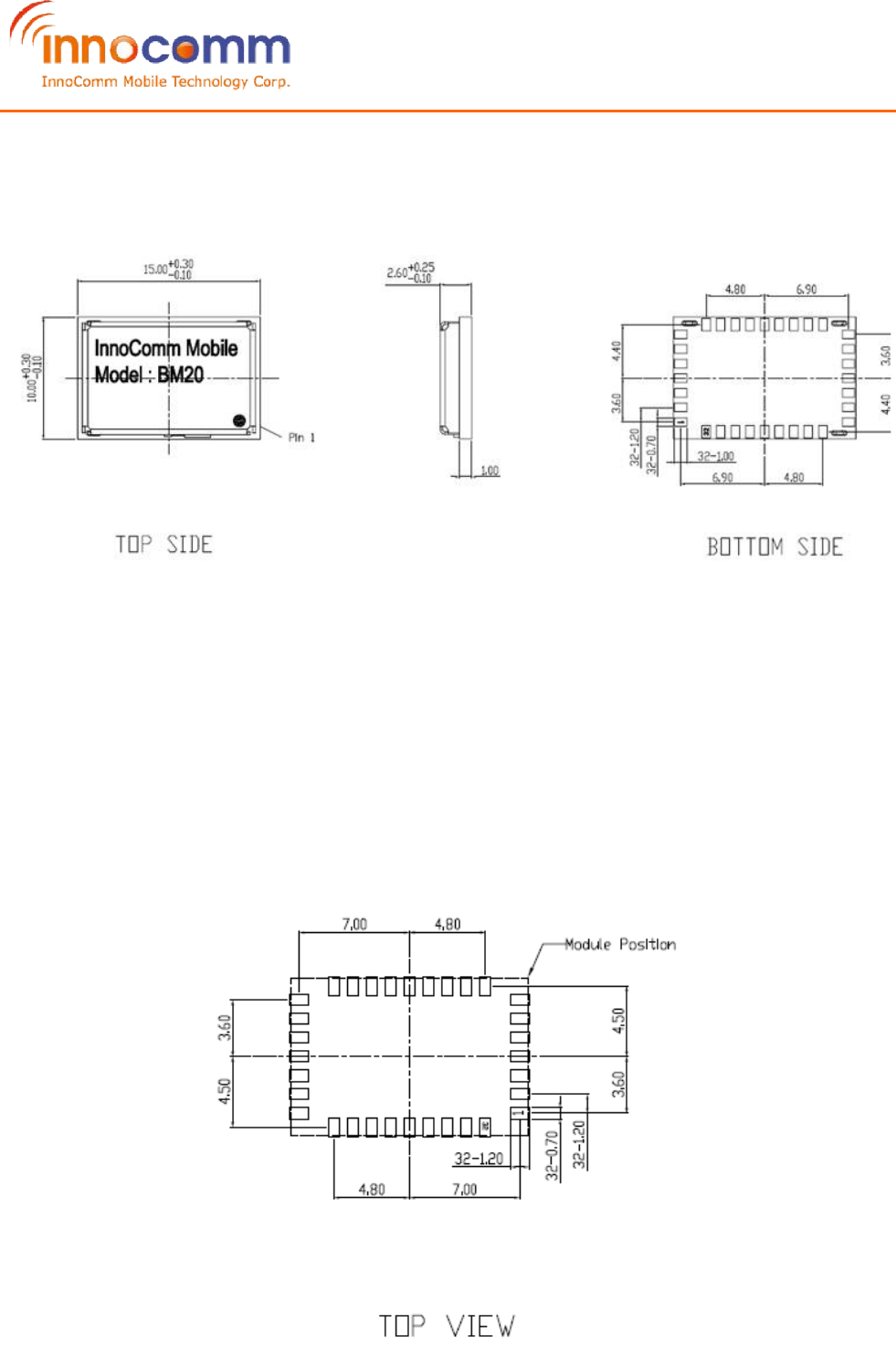
Outline
•
15.0 mm(L) × 10.0 mm(W) × 2.6 mm(H),
•
32 pin LGA Package
Application
•
Computer peripherals and I/O devices
•
Mouse
•
Keyboard
•
Mobile HID
•
CE remote controls
•
Network processor
•
Wearable
•
Virtual reality headsets
•
Health and medical
•
Enterprise lighting
•
Industrial
•
Commercial
•
Retail
•
Beacons
•
Connectivity device in multi-chip solutions

BM20 Module Product Specification
05/31/2018
REV 1.0
6/14
InnoComm Mobile Technology
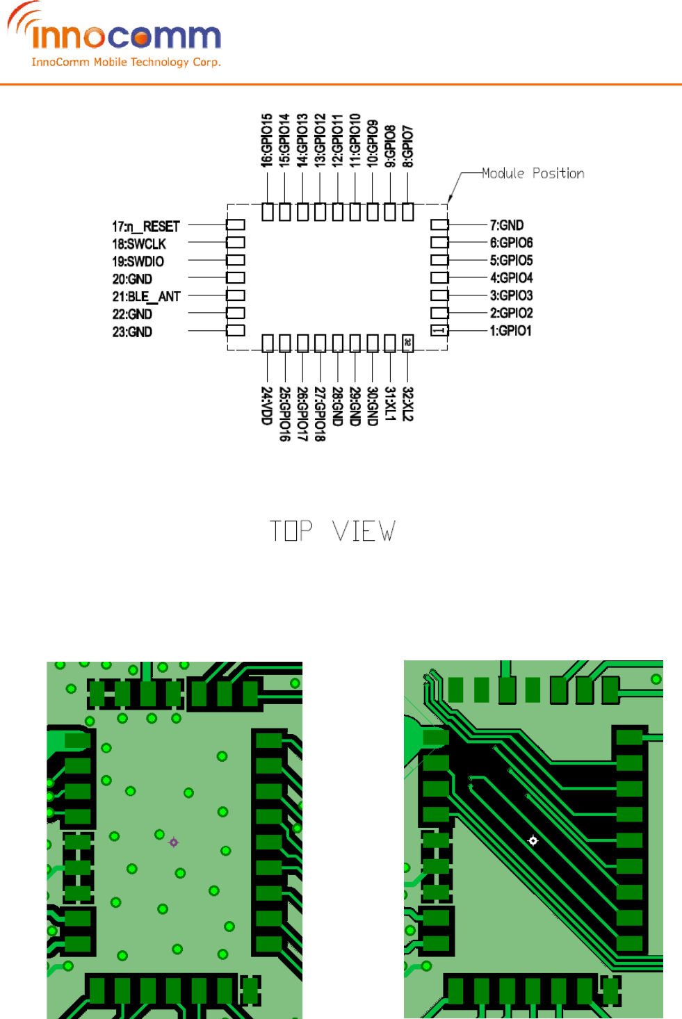
3.
PIN Map and Signal Description
Pin #
Pin Name
Description
1
GPIO1
Analog/Digital, SAADC/COMP/LPCOMP input
2
GPIO2
Analog/Digital, SAADC/COMP/LPCOMP input
3
GPIO3
Analog/Digital, SAADC/COMP/LPCOMP input
4
GPIO4
Analog/Digital, SAADC/COMP/LPCOMP input
5
GPIO5
Digital
6
GPIO6
Digital
7
GND
Ground
8
GPIO7
Digital
9
GPIO8
NFC/Digital
10
GPIO9
NFC/Digital
11
GPIO10
Digital
12
GPIO11
Digital
13
GPIO12
Digital
14
GPIO13
Digital
15
GPIO14
Digital
16
GPIO15
Digital
17
n_RESET
Reset, active Low, with internal pull–up
18
SWCLK
BLE Debug/download
19
SWDIO
BLE Debug/download
20
GND
Ground
21
BLE_ANT
BLE Antenna
22
GND
Ground
23
GND
Ground
24
VDD
Module Power in
25
GPIO16
Digital
26
GPIO17
Analog/Digital,SAADC/COMP/LPCOMP input
27
GPIO18
Analog/Digital,SAADC/COMP/LPCOMP input
28
GND
Ground
29
GND
Ground
30
GND
Ground
31
XL1
Connection for 32.768 kHz crystal
32
XL2
Connection for 32.768 kHz crystal
BM20 Module Product Specification
05/31/2018
REV 1.0
7/14
InnoComm Mobile Technology
4.
ELECTRICAL CHARACTERISTICS
4.1
Recommended Operating Range
PARAMETER
CONDITIONS
MIN TYP MAX UNIT
Operating
ambient temperature
range,
T
A
–40 25 85 C
Supply
rise time (0 V to 1.7 V) 60 ms
Operating
supply voltage, VDD 1.7 3.0 3.6 V
Important: Power-on reset circuitry may not function properly for rise times longer than the specified maximum.
4.2
Power Consumption
PARAMETER
CONDITIONS
MIN TYP
MAX
UNIT
TX
supply current at maximum output
power(+4dBm)
25
mA
RX
16
mA
System
Off mode
0.7
uA
4.3
I/O Characteristics
PARAMETER
MIN
TYP
MAX
UNIT
Voltage at digital I/O pins
-0.3
VDD + 0.3
V
Input Low voltage level(VIL)
0.3xVDD
V
Input High voltage level(VIH)
0.7xVDD
VDD
V
Output Low Voltage level(VOL)
0.4
V
Output Low Voltage level(VOH)
VDD-0.4
VDD
V
BM20 Module Product Specification
05/31/2018
REV 1.0
8/14
InnoComm Mobile Technology
5.
RF CHARACTERISTICS
TX:
Following characteristics are valid for conditions as follows (unless otherwise specified)
Tamb = -20 °C to 85 °C, VCC = 3.3 V
Bursts: 10, Payload: PRBS 9, Length: 37 Bytes
MIN
TYP MAX UNIT
Maximum TX Power 3.3 dBm
1st Adjacent Channel Transmit Power 1 MHz (1
Msps)
-25 dBc
2nd Adjacent Channel Transmit Power 2 MHz (1
Msps)
-50 dBc
1st Adjacent Channel Transmit Power 2 MHz (2
Msps)
-25 dBc
2nd Adjacent Channel Transmit Power 4 MHz (2
Msps)
-50 dBc
RX:
Following characteristics are valid for conditions as follows (unless otherwise specified)
Tamb= -20 °C to 85 °C, VCC = 3.3 V
PARAMETER MIN TYP MAX UNIT
Receiver Sensitivity -95 dBm
BM20 Module Product Specification
05/31/2018
REV 1.0
9/14
InnoComm Mobile Technology
6.
Mechanical Information
7.
PCB Layout Recommendation
BM20 Module Product Specification
05/31/2018
REV 1.0
10/14
InnoComm Mobile Technology
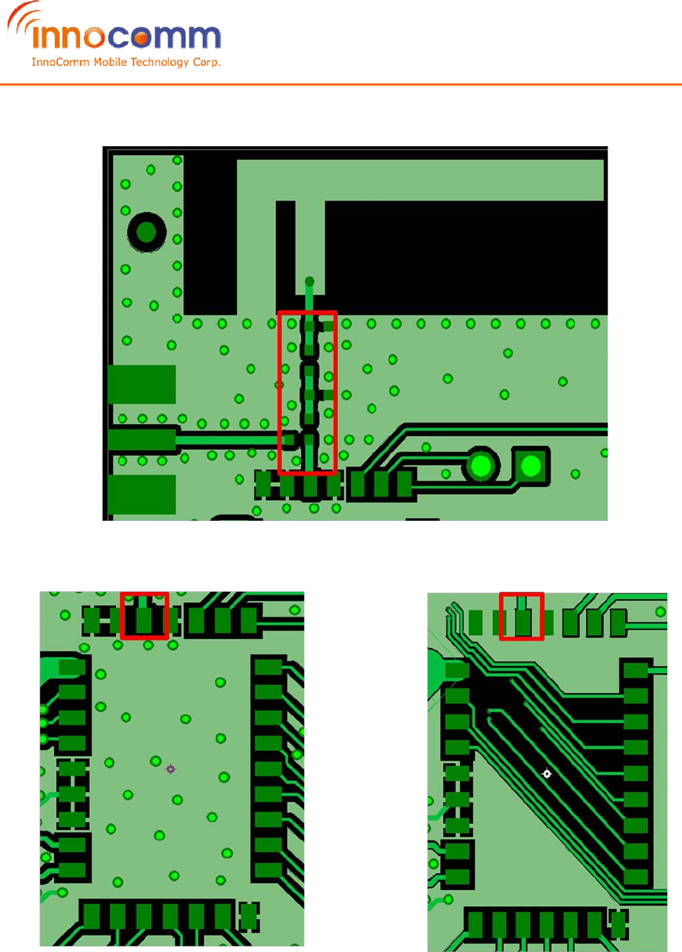
8.
Module Layout Guide
1.
Do not route traces under module to minimize on interference.
(O)
(X)
BM20 Module Product Specification
05/31/2018
REV 1.0
11/14
InnoComm Mobile Technology
2.
The trace Impedance of the antenna port (Pin 21) is 50 Ω. In order to minimize
the return loss, it is recommended to use short traces.
3.
Keep enough clearance between the antenna port (Pin 21) and surrounding
GND to minimize the power loss.
(O)
(X)
BM20 Module Product Specification
05/31/2018
REV 1.0
12/14
InnoComm Mobile Technology
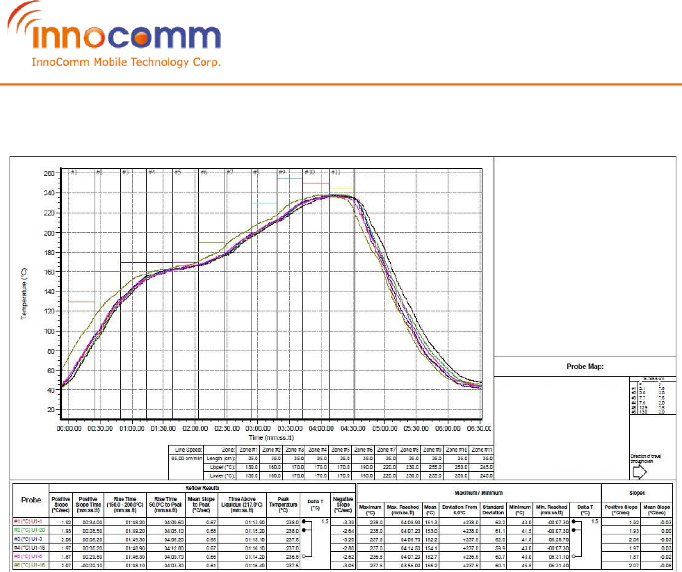
9.
SMT Solder Reflow Recommendation
Note: Allowable reflow soldering times: 2 times base on recommended reflow profile.

BM20 Module Product Specification
05/31/2018
REV 1.0
13/14
InnoComm Mobile Technology
10.
Appendix
BM20 nRF52832_QFN48
Pin Number
Pin Name
Pin Number
Pin Name
Type
1
GPIO1
4
P0.02
Analog/Digital
2
GPIO2
5
P0.03
Analog/Digital
3
GPIO3
6
P0.04
Analog/Digital
4
GPIO4
7
P0.05
Analog/Digital
5
GPIO5
8
P0.06
Digital
6
GPIO6
9
P0.07
Digital
8
GPIO7
10
P0.08
Digital
9
GPIO8
11
P0.09
NFC/Digital
10
GPIO9
12
P0.10
NFC/Digital
11
GPIO10
14
P0.11
Digital
12
GPIO11
15
P0.12
Digital
13
GPIO12
18
P0.15
Digital/Trace port
14
GPIO13
21
P0.18
Digital/Trace port
15
GPIO14
22
P0.19
Digital
16
GPIO15
23
P0.20
Digital/Trace port CLK
17
nReset
24
P0.21
Digital/Reset
25
GPIO16
37
P0.25
Digital
26
GPIO17
41
P0.29
Analog/Digital
27
GPIO18
43
P0.31
Analog/Digital
IO Mapping table

BM20 Module Product Specification
05/31/2018
REV 1.0
Federal Communications Commission Statement
This device complies with FCC Rules Part 15. Operation is subject to the following two conditions:
•This device may not cause harmful interference.
•This device must accept any interference received, including interference that may cause undesired
operation.
This equipment has been tested and found to comply with the limits for a class B digital device, pursuant to
Part 15 of the Federal Communications Commission (FCC) rules. These limits are designed to provide
reasonable protection against harmful interference in a residential installation. This equipment generates,
uses, and can radiate radio frequency energy and, if not installed and used in accordance with the
instructions, may cause harmful interference to radio communications. However, there is no guarantee
that interference will not occur in a particular installation. If this equipment causes harmful interference to
radio or television reception, which can be determined by turning the equipment off and on, the user is
encouraged to try to correct the interference by doing one or more of the following measures:
•Reorient or relocate the receiving antenna.
•Increase the separation between the equipment and receiver.
•Connect the equipment into an outlet on a circuit different from that to which the receiver is connected.
•Consult the dealer or an experienced radio/TV technician for help.
FCC Caution
Any changes or modifications not expressly approved by the party responsible for compliance could void
the user‘s authority to operate the equipment.
The antenna(s) used for this transmitter must not be co-located or operating in conjunction with any other
antenna or transmitter.
Radiation Exposure Statement:
This equipment complies with FCC radiation exposure limits set forth for an uncontrolled environment. End
users must follow the specific operating instructions for satisfying RF exposure compliance. To maintain
compliance with FCC exposure compliance requirement, please follow operation instruction as
documented in this manual.
FCC Label Instructions:
The outside of final products that contains this module device must display a label
referring to the enclosed module. This exterior label can use wording such as: “Contains
Transmitter Module FCC ID:YAIBM20”,or “Contains FCC ID: YAIBM20”, Any similar wording that expresses
the same meaning may be used.
14/14