InnoComm Mobile Technology SN10-12 SigFox module User Manual rev 4
InnoComm Mobile Technology Corporation SigFox module rev 4
User Manual rev 4.pdf

SN10-12 SIGFOX Module
User Manual
FCC ID: YAISN10-12
Model Name SN10-12
Project code
Description SIGFOX module
Version 0.5
Issue Date 2017/05/26
Approved by Reviewed by Issued by
Harrison Chen Taka Wei Iestyn Chen

SN10-12
7/12/2017
REV 0.5
InnoComm Mobile Technology Confidential
2
/
14
Revision History
Revision Released Date Comments/Remark Author
0.1 2017/03/14 Initial release Iestyn Chen
0.2 2017/03/17 Update with RX performance spec. Iestyn Chen
0.3 2017/03/24 Add module layout guide and appendix section Iestyn Chen
0.4 2017/03/29 Update RX value, reflow profile Iestyn Chen
0.5 2017/05/26 Modify FCC Interference Statement Keller Lin
® 2017 InnoComm Mobile Technology Corp.
GENERAL NOTICE
THE USE OF THE PRODUCT INCLUDING THE SOFTWARE AND DOCUMENTATION (THE "PRODUCT") IS SUBJECT TO THE
RELEASE NOTE PROVIDED TOGETHER WITH THE PRODUCT. IN ANY EVENT THE PROVISIONS OF THE RELEASE NOTE
SHALL PREVAIL. THIS DOCUMENT CONTAINS INFORMATION ABOUT INNOCOMM PRODUCTS. THE SPECIFICATIONS IN
THIS DOCUMENT ARE SUBJECT TO CHANGE AT INNOCOMM'S DISCRETION. INNOCOMM MOBILE TECHNOLOGY
GRANTS A NON-EXCLUSIVE RIGHT TO USE THE PRODUCT. THE RECIPIENT SHALL NOT TRANSFER, COPY, MODIFY,
TRANSLATE, REVERSE ENGINEER, CREATE DERIVATIVE WORKS; DISASSEMBLE OR DECOMPILE THE PRODUCT OR
OTHERWISE USE THE PRODUCT EXCEPT AS SPECIFICALLY AUTHORIZED. THE RECIPIENT UNDERTAKES FOR AN
UNLIMITED PERIOD OF TIME TO OBSERVE CONFIDENTIALLITY REGARDING ANY INFORMATION AND DATA PROVIDED
TO THEM IN THE CONTEXT OF THE DELIVERY OF THE PRODUCT. THIS GENERAL NOTE
SHALL BE GOVERNED AND CONSTRUED ACCORDING TO TAIWAN LAW.
Copyright
Transmittal, reproduction, dissemination and/or editing of this document as well as utilization of its contents and
communication thereof to others without express authorization are prohibited. Offenders will be held liable for
payment of damages. All rights created by patent grant or registration of a utility model or design patent are reserved.
Copyright © 2017, InnoComm Mobile Technology Corp.
Trademark Notice
InnoComm® is the trademarks of InnoComm Mobile Technology Corp.
Other trademarks and registered trademarks mentioned herein are the property of their respective owners.

SN10-12
7/12/2017
REV 0.5
InnoComm Mobile Technology Confidential
3
/
14
TABLE OF CONTENT
1. INTRODUCTION ......................................................................................... 4
1.1. KEY FEATURES ............................................................................................................. 4
2.ELECTRICAL CHARACETRISTICS ............................................................. 5
2.1 RECOMMENDED OPERATING RANGE .................................................................................... 5
2.2 POWER CONSUMPTION .................................................................................................... 5
2.3 CHARACTERIZATION INFORMATION ...................................................................................... 5
3. RF CHARACTERISTICS .............................................................................. 6
4. SN10-12 PIN MAP AND SIGNAL DESCRIPTION....................................... 7
5. MODULE INSTALLATION GUIDE ............................................................... 8
5.1MECHANICAL INFORMATION .................................................................. 8
5.2. PCB LAYOUT FOOTPRINT ...................................................................... 8
5.3. MODULE INSTALLATION NOTICE ......................................................... 9
5.4. SMT SOLDER REFLOW NOTICE: ......................................................... 10
5.5. ANTENNA ............................................................................................... 11
6. APPENDIX .................................................................................................. 12
6.1 SW USER GUIDE INFORMATION. ......................................................... 12
FEDERAL COMMUNICATION COMMISSION INTERFERENCE STATEMENT .............. 13
RADIATION EXPOSURE STATEMENT: .......................................................................... 14
SN10-12
7/12/2017
REV 0.5
InnoComm Mobile Technology Confidential
4
/
14
1. Introduction
The IoT presents a different set of communications challenges to those faced by the conventional
internet or cellular networks. Unlike cellphones and computers, IoT devices do not need to
transfer large amounts of data. However, requirements for battery life and hardware cost are
much more stringent and difficult to meet. For example, a soil moisture sensor might send a single
moisture reading – one number – every hour. But to be practical for the farmer the batteries in
the sensor need to last for at least one growing season, and ideally several years.
SIGFOX networks provide a simplified way to connect low energy isolated devices to customer’s
applications on wide territories, through a high efficiency radio technology with extreme budget
links despite low radiations and at very low costs. Customers can then build their applications
without any concern of the heavy radio network problematic and management, and, almost, no
concern of the radio communication aspects.
The SN10-12 is a transceiver module which complies with SIGFOX network specifications. The
SN10-12 is based on NXP OL2385 chip which is a Sub-GHz wireless SoC transceiver. The SN10-12
module provides a wide range of frequency selections for IoT applications network service
platform.
1.1. Key Features
• High performance low power RISC micro-controller
• Memory
• 32kB EROM
• 7kB RAM
• Ultra Narrow Band Radio
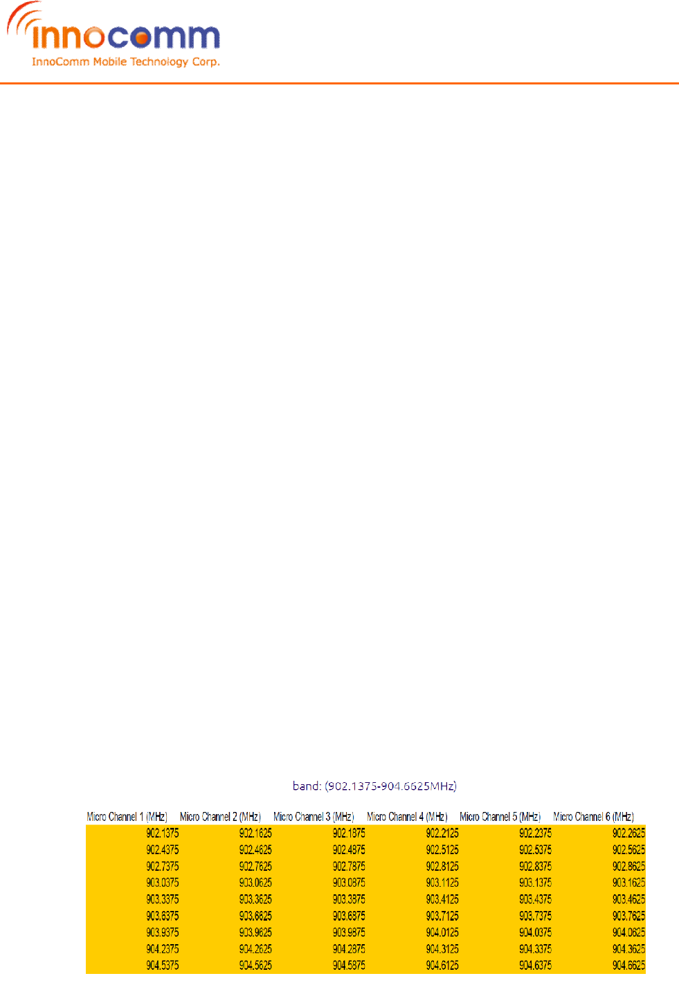
• Frequency Band:
TX: 902.1375-904.6625MHz
RX: 905.2 MHz
• Output Power : 23.62 dBm
SN10-12
7/12/2017
REV 0.5
InnoComm Mobile Technology Confidential
5
/
14
• Excellent Receiving Sensitivity: -125dBm @600bps 2GFSK
• Excellent Image Rejection: 60 dB
• Excellent Blocking Performance: 58 dB
2.ELECTRICAL CHARACETRISTICS
2.1 Recommended Operating Range
PARAMETER CONDITIONS MIN
TYP
MAX UNIT
Operating temperature range
–
40
25
85 °C
Operating supply voltage 3.3
3.6 V
2.2 Power Consumption
PARAMETER CONDITIONS MIN
TYP
MAX UNIT
TX supply current at
maximum output power @22dBm, 3.3V 240
260 mA
RX
16.5 17.5 mA
2.3 Characterization information
PARAMETER CONDITIONS MIN
TYP
MAX UNIT
Voltage at digital I/O pins -0.3
VDD + 0.3 V
SN10-12
7/12/2017
REV 0.5
InnoComm Mobile Technology Confidential
6
/
14
3. RF Characteristics
PARAMETER Model TX / RX UNIT Note
Center Frequency SN10-12 902.2 / 905.2 MHz SIGFOX
RCZ2
PARAMETER CONDITIONS MIN TYP MAX UNIT Note
Antenna port impedance
50 Ω
TX Characteristics
Following characteristics are valid for conditions as follows (unless otherwise specified)
Tamb = -40 °C to 85 °C, VSS = 0 V, VDD = 2.6 V to 3.6 V, crystal = 55.2 MHz
PARAMETER CONDITIONS MIN TYP MAX UNIT Note
Maximum output
power, CW mode
SN10-12 21 22 dBm
RX Characteristics
Following characteristics are valid for conditions as follows (unless otherwise specified)
2GFSK modulation, h = 2.67, BT = 1.0, NRZ, data-rate = 0.6 kChips/s, Channel spacing = 10 kHz,
Channel filter bandwidth = 10 kHz, Frame Error Rate (FER) = 20%, payload length = 228 byte,
crystal = 55.2 MHz.
Tamb = 25 °C, VDD = 2.6 V to 3.6 V, fC = 905 MHz
PARAMETER CONDITIONS MIN TYP MAX UNIT Note
Sensitivity -40 °C to 85 °C -125 dBm PER at
10% on
1000
frames
sent.
Co-channel rejection 2GFSK jammer
2 5 dB
Adjacent channel
rejection
Channel filter
BW = 10 kHz,
jammer same
modulation as
wanted.
Channel
separation:
10 kHz, 20 kHz,
150 kHz.
50 55 dB
55 60 dB
60 65 dB
SN10-12
7/12/2017
REV 0.5
InnoComm Mobile Technology Confidential
7
/
14
4. SN10-12 PIN Map and Signal Description
Pin # Pin Name
Type Description
1 GND GND Ground
2 VDD Power Power Supply input
3 GND GND Ground
4 GND GND Ground
5 GND GND Ground
6 GND GND Ground
7 GND GND Ground
8 GND GND Ground
9 P16 Digital I/O GPIO, SPI_SDI
10 P15 Digital I/O GPIO, SPI_CS
11 GND GND Ground
12 GND GND Ground
13 P14 Digital I/O GPIO, SPI_SCLK
14 P13 Digital I/O GPIO, SPI_SDO, UART_TX
15 P12 Digital I/O GPIO, UART_RX
16 P11 Digital I/O Debug port, INT, Optional
17 P10 Digital I/O GPIO, UART TX/RX CLOCK
18 RST_N Digital I/O GPIO, RESET
19 MDI_MSDA
Digital I/O Debug port, MSDA
20 MDI_MSCL Digital I/O Debug, MSCL
21 GND GND Ground
22 P17 Digital I/O GPIO, SPI_AK
23 P20 Digital I/O Debug port, RSSI LOG
24 P21 Digital I/O N.C.
25 P22 Digital I/O N.C.
26 P23 Digital I/O GPIO
27 GND GND Ground
28 IF_IFN Digital I/O GPIO, IFN
29 IF_IFP Digital I/O GPIO, IFP
30 GND GND Ground
31 ANT RF RF Antenna Interface
Impedance=50 Ω
32 GND GND Ground
SN10-12
7/12/2017
REV 0.5
InnoComm Mobile Technology Confidential
8
/
14
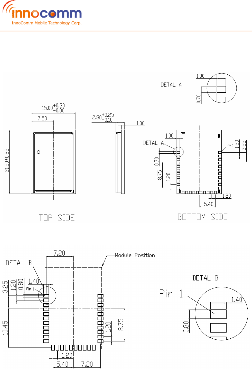
5. Module installation Guide
5.1Mechanical Information
5.2. PCB Layout Footprint
SN10-12
7/12/2017
REV 0.5
InnoComm Mobile Technology Confidential
9
/
14
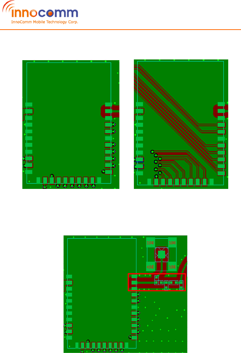
5.3. Module installation Notice
5.3.1 Do not route traces under module to minimize on interference.
(O) (X)
5.3.2
The trace Impedance of the antenna port (Pin 31) is 50 Ω. In order to minimize the return loss, it
is recommended to use short traces.
SN10-12
7/12/2017
REV 0.5
InnoComm Mobile Technology Confidential
10
/
14
5.3.3
Keep enough clearance between the antenna port (Pin 31) and surrounding GND to minimize
the power loss.
(O) (X)
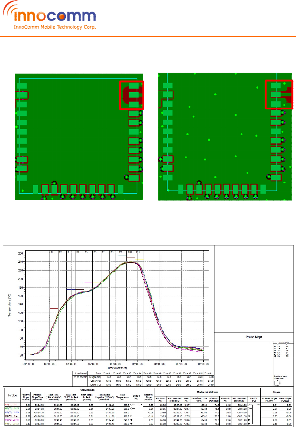
5.4 . SMT Solder Reflow Notice:
Note: Allowable reflow soldering times: 2 times base on recommended reflow profile.

SN10-12
7/12/2017
REV 0.5
InnoComm Mobile Technology Confidential
11
/
14
5.5 Antenna design declaration:
To compliance FCC KDB 996369 D01 v02 cause II. This module can only be used with a host
antenna circuit trace layout design in strict compliance with the InnoComm instructions provided.
The SN10-12 module use trace antenna in fixture board and compliance 47 CFR FCC Part 15
Subpart C (Section 15.247). For proper integration our modules in end products, we shall provided
detailed and comprehensive instructions. Integrator, or end-user who use new antenna design
will need to apply another FCCID and compliance FCC requirement.,
Antenna design Notice:
Follow notice in section 5.3.2 and 5.3.3., the trace Impedance of the antenna port (Pin 31) is 50 Ω.

SN10-12
7/12/2017
REV 0.5
InnoComm Mobile Technology Confidential
12
/
14
Appendix
6.1 SW User Guide information.
The SIGFOX software driver supports MCUs. These MCUs are a subset
of the MCUs supported by the Kinetis Software Development Kit (KSDK) layer.
This SW driver is built on the Analog Middleware Layer (AML), which creates an
API abstraction layer for the desired Software Development Kit (SDK).
The current implementation includes abstractions for KSDK 2.0 and S32 SDK. This allows support to
be added for additional layers, such as the KSDK, without having to change the SIGFOX Software Driver
itself.
The detail Commend and SPI please read the web link as below.
SigFox Software driver user guide
http://cache.nxp.com/assets/documents/data/en/user-
guides/OL2385SWUG.pdf?fsrch=1&sr=9&pageNum=1:

SN10-12
7/12/2017
REV 0.5
InnoComm Mobile Technology Confidential
13
/
14
Federal Communication Commission Interference Statement
This device complies with Part 15 of the FCC Rules. Operation is subject to the following
two conditions: (1) This device may not cause harmful interference, and (2) this device
must accept any interference received, including interference that may cause undesired
operation.
This equipment has been tested and found to comply with the limits for a Class B digital
device, pursuant to Part 15 of the FCC Rules. These limits are designed to provide
reasonable protection against harmful interference in a residential installation. This
equipment generates, uses and can radiate radio frequency energy and, if not installed and
used in accordance with the instructions, may cause harmful interference to radio
communications. However, there is no guarantee that interference will not occur in a
particular installation. If this equipment does cause harmful interference to radio or
television reception, which can be determined by turning the equipment off and on, the
user is encouraged to try to correct the interference by one of the following measures:
- Reorient or relocate the receiving antenna.
- Increase the separation between the equipment and receiver.
- Connect the equipment into an outlet on a circuit different from that
to which the receiver is connected.
- Consult the dealer or an experienced radio/TV technician for help.
FCC Caution: Any changes or modifications not expressly approved by the party responsible
for compliance could void the user's authority to operate this equipment.
This transmitter must not be co-located or operating in conjunction with any other
antenna or transmitter.
SN10-12
7/12/2017
REV 0.5
InnoComm Mobile Technology Confidential
14
/
14
Radiation Exposure Statement:
This equipment complies with FCC radiation exposure limits set forth for an uncontrolled
environment. This equipment should be installed and operated with minimum distance
20cm between the radiator & your body.
This device is intended only for OEM integrators under the following conditions:
1) The antenna must be installed such that 20 cm is maintained between the antenna and
users, and
2) The transmitter module may not be co-located with any other transmitter or antenna.
3) Module approval valid only when the module is installed in the tested host or compatible
series of host which have similar RF exposure characteristic with equal or larger antenna
separation distance.
As long as 3 conditions above are met, further transmitter test will not be required. However,
the OEM integrator is still responsible for testing their end-product for any additional
compliance requirements required with this module installed
IMPORTANT NOTE: In the event that these conditions can not be met (for example certain
laptop configurations or co-location with another transmitter), then the FCC authorization is
no longer considered valid and the FCC ID can not be used on the final product. In these
circumstances, the OEM integrator will be responsible for re-evaluating the end product
(including the transmitter) and obtaining a separate FCC authorization.
End Product Labeling
This transmitter module is authorized only for use in device where the antenna may be
installed such that 20 cm may be maintained between the antenna and users. The final end
product must be labeled in a visible area with the following: “Contains FCC ID:YAISN10-12”.
The grantee's FCC ID can be used only when all FCC compliance requirements are met.
Manual Information To the End User
The OEM integrator has to be aware not to provide information to the end user regarding
how to install or remove this RF module in the user’s manual of the end product which
integrates this module.
The end user manual shall include all required regulatory information/warning as show in
this manual.