Intec Automation 5208EVB 32-BIT MICROCONTROLLER User Manual WildFire Users Manual
Intec Automation Inc. 32-BIT MICROCONTROLLER WildFire Users Manual
UserManual.wiki
>
Intec Automation
>
5208EVB User Manual
users manual
Navigation menu
Upload a User Manual
Namespaces
Wiki Guide
HTML
PDF
Info
Views
User Manual
Discussion / Help
Navigation


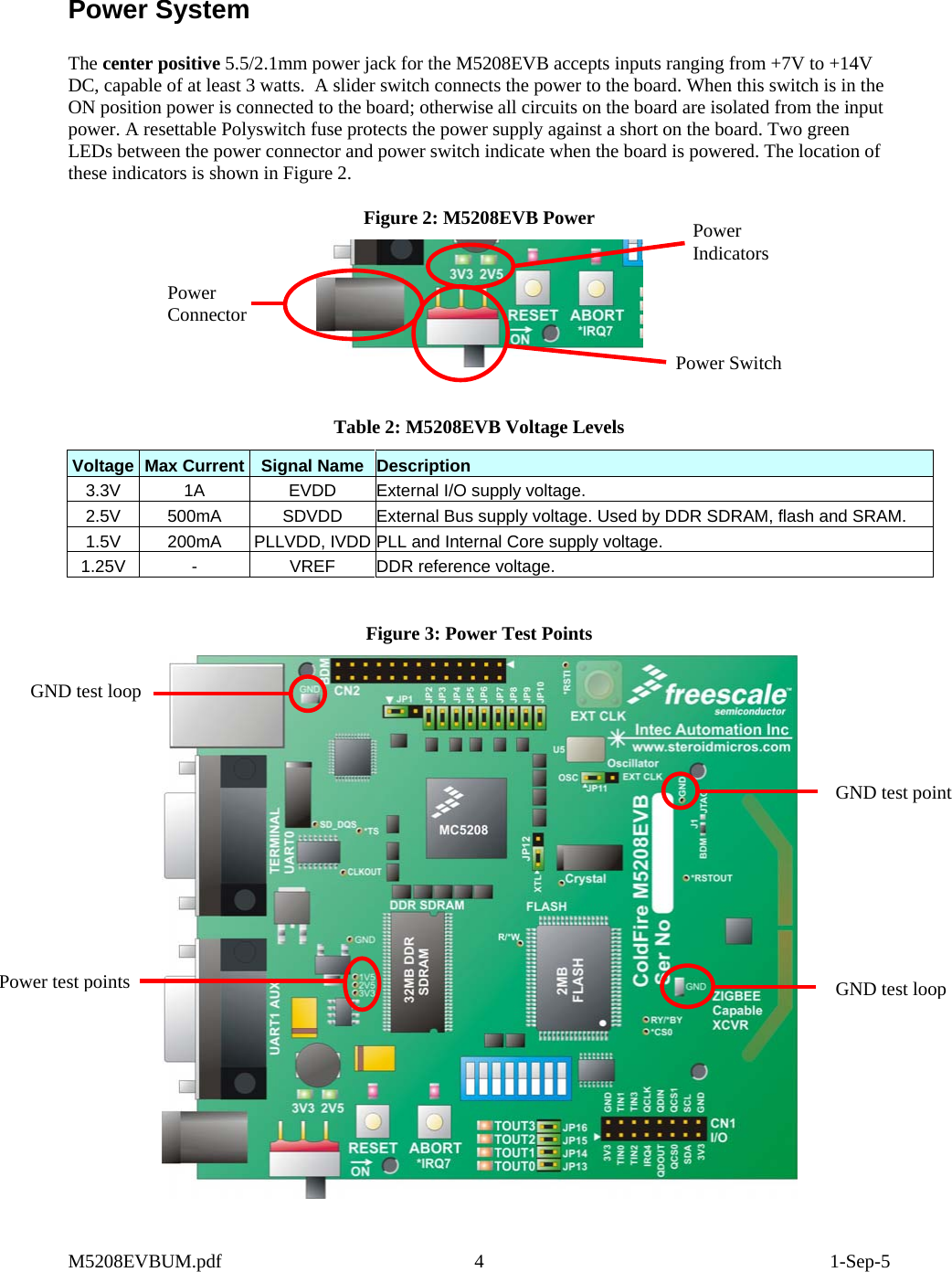
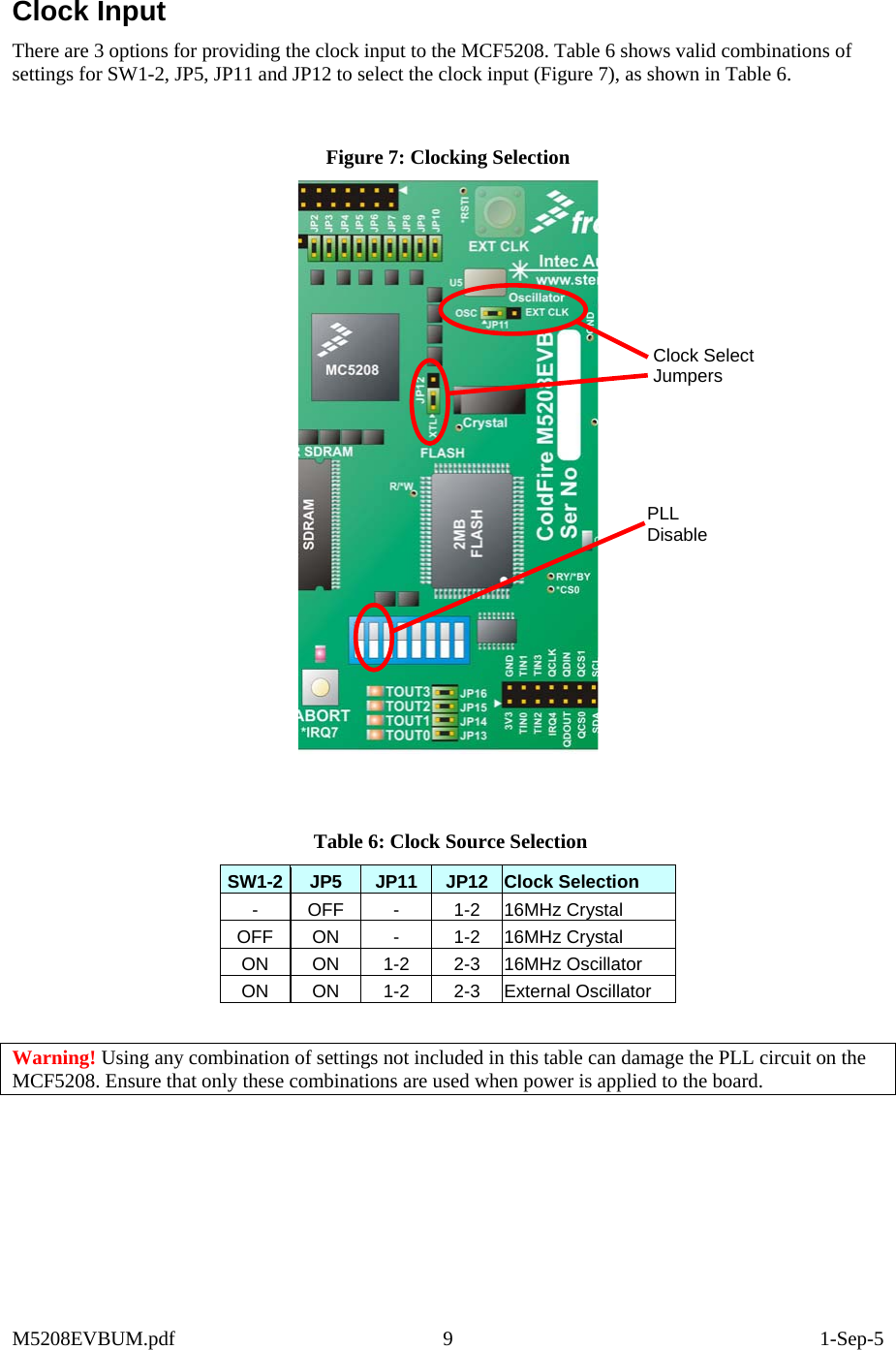
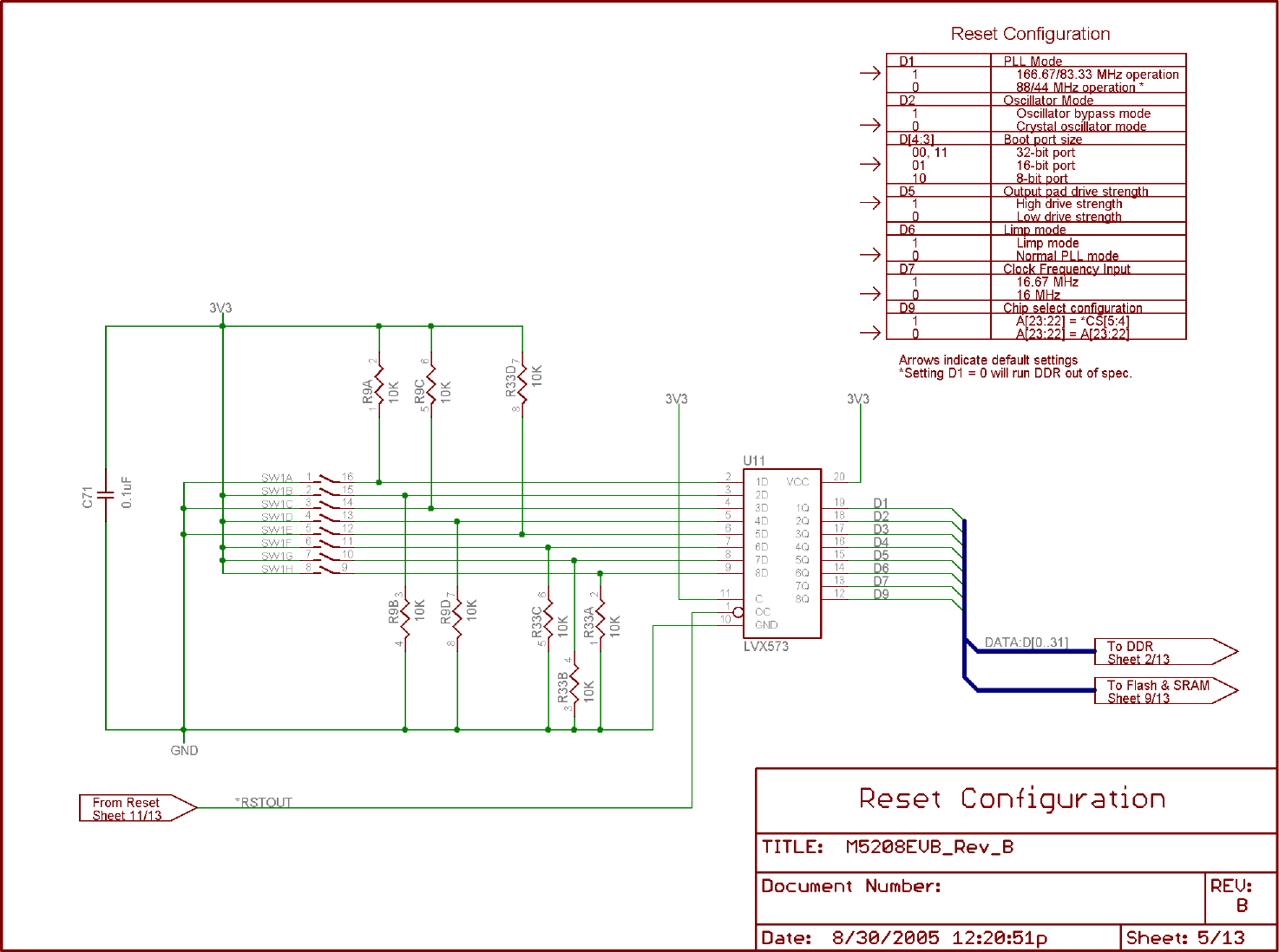
![Reset There are 3 ways to reset the M5208EVB: Power-on reset – accomplished by power cycling the board: switch the power switch to the OFF position then back to the ON position or remove and reconnect the power cable. The contents of all volatile memory (iRAM and SDRAM) will be lost. External reset – asserted by pressing the Reset button or by issuing a reset command through the BDM pod using software on the PC. The contents of volatile memory are preserved. Software reset – invoked with the ‘reset’ command to dBUG monitor, the ‘reboot’ command in uClinux, or by setting bit 7 in the RCR register (see MCF5208 Reference Manual, “Chapter 10 Reset Controller Module”). The contents of volatile memory are preserved. In all 3 cases, when the board is reset, all registers are reset to their default state. Figure 5: Reset Signal and Switch Locations *RSTI test point*RCON Jumper (JP5) *RSTOUT test point Reset button Power switch Reset LED *RCON Switch (SW1) Startup Configuration The MCF5208 configuration depends on 9 signals: *RCON, D9 and D[7:1] which are sampled when the MPU comes out of reset. When *RCON is asserted (the shunt on JP5 is on), the MCF5208 reads its configuration options from the data signals which are driven high or low by the 8 rocker switches on SW1. Configuration options are shown in Table 4. If *RCON is negated (JP5 OFF), the MCF5208 takes the default reset configuration values shown in Table 5. M5208EVBUM.pdf 6 1-Sep-5](https://usermanual.wiki/Intec-Automation/5208EVB/User-Guide-580592-Page-13.png)
![Table 4: RCON Mode Configuration Selection (*RCON = 0 Å JP5 ON) Selection Configuration SW1-1 PLL Mode OFF 166.67MHz Core bus, 83.33MHz External Bus operation ON 88MHz Core bus, 44MHz External Bus operation (Note 1) SW1-2 Oscillator Mode OFF Crystal oscillator mode ON Oscillator bypass mode SW1-3 SW1-4 Boot Port Size OFF OFF 16-bit port OFF ON 32-bit port ON OFF 32-bit port ON ON 8-bit port SW1-5 Output Pad Drive Strength OFF High drive strength ON Low drive strength SW1-6 LIMP Mode OFF Normal operation; PLL drives internal clocks. ON LIMP mode; low-power clock divider drives internal clocks. SW1-7 Oscillator Frequency Select OFF 16MHz is used as input to processor ON 16.67MHz is used as input to processor SW1-8 Chip Select Configuration OFF A[23:22] = A[23:22] ON A[23:22] = *FB_CS[5:4] NOTE: Default setting for each switch is OFF Table 5: Default RCON Values (*RCON = 1; Å JP5 OFF) Selection Default Mode PLL Mode 88MHz Core bus, 44MHz External Bus operation (Note 1) Oscillator Mode Crystal oscillator mode Boot Port Size 32-bit port Output Pad Drive Strength Low drive strength LIMP Mode Normal operation; PLL drives internal clocks. Oscillator Frequency Select 16MHz is used as input to processor Chip Select Configuration A[23:22] = A[23:22] Note 1: Caution! Loss of Functionality. Running the PLL at 88/44MHz will run the DDR out of spec. The DDR will be inaccessible under this configuration. M5208EVBUM.pdf 7 1-Sep-5](https://usermanual.wiki/Intec-Automation/5208EVB/User-Guide-580592-Page-14.png)
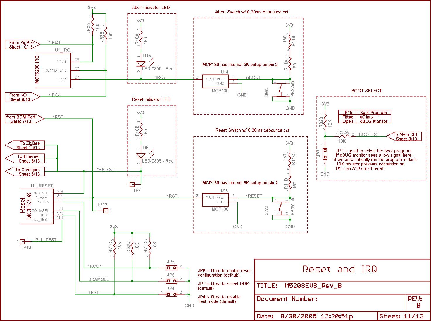
![IRQ The MCF5208 EPORT module has 3 signals (IRQ1, IRQ4 and IRQ7) that can be individually configured as digital inputs or outputs or they can be configured to be edge or level sensitive interrupt signals. If a signal is configured for edge detection, it can detect on a rising edge, falling edge or both. All IRQ pins are configured as digital input out of reset. *IRQ1 is used as in interrupt from the MC13192 ZigBee Capable Transceiver. IRQ7 is connected to the Abort button on the M5208EVB. When the board first starts up, the dBUG monitor configures *IRQ7 as a falling edge interrupt. This leaves *IRQ4 for user control. The location of the Abort switch and *IRQ4 pin is shown in Figure 14. Figure 14: Abort Switch and *IRQ4 Locations *IRQ4Abort Button Interrupt Level and Priority An understanding of the interrupt level and priority scheme on the MCF5208 can be helpful. The MCF5208 has sources of interrupts. Each is assigned a number ranging from 1 for IRQ1 to 62 for buss error. These are hard wired. With the exception of the IRQ signals, each interrupt source (eg. source 4, PIT0/PCSR0[PIF] PIT interrupt flag) can be assigned an interrupt level, 1 being the lowest level, 7 being the highest (serviced first). Any number of interrupts can be set to the same level. When multiple interrupts at the same level fire, they are processed in reverse order of their source number. That is, the lowest source gets serviced last. And, the IRQ signals correspond to the lowest sources, as shown in Table 9. Table 9: IRQ Pin Priority Signal Source/Priority*IRQ1 1 *IRQ4 2 *IRQ7 3 This interrupt scheme can have interesting side effects. For instance, in the [absurd] case where the Ethernet interrupts were set to level 7, the level 7 interrupt fired by pressing the Abort button would not be serviced until the CPU had finished servicing the Ethernet interrupts. dBUG monitor sets the *IRQ7 level to level 7. Internal interrupt sources should not be set to level 7 or the Abort functionality of dBUG monitor will be compromised. The MCF5208’s interrupt scheme is covered in great detail in Freescale’s MCF5208 Reference Manual Ch. 14 – Interrupt Controller Module and Ch. 15 – Edge Port Module. M5208EVBUM.pdf 15 1-Sep-5](https://usermanual.wiki/Intec-Automation/5208EVB/User-Guide-580592-Page-22.png)


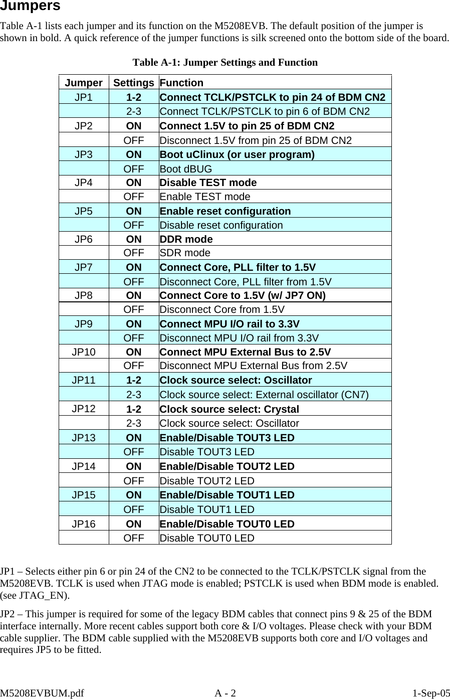
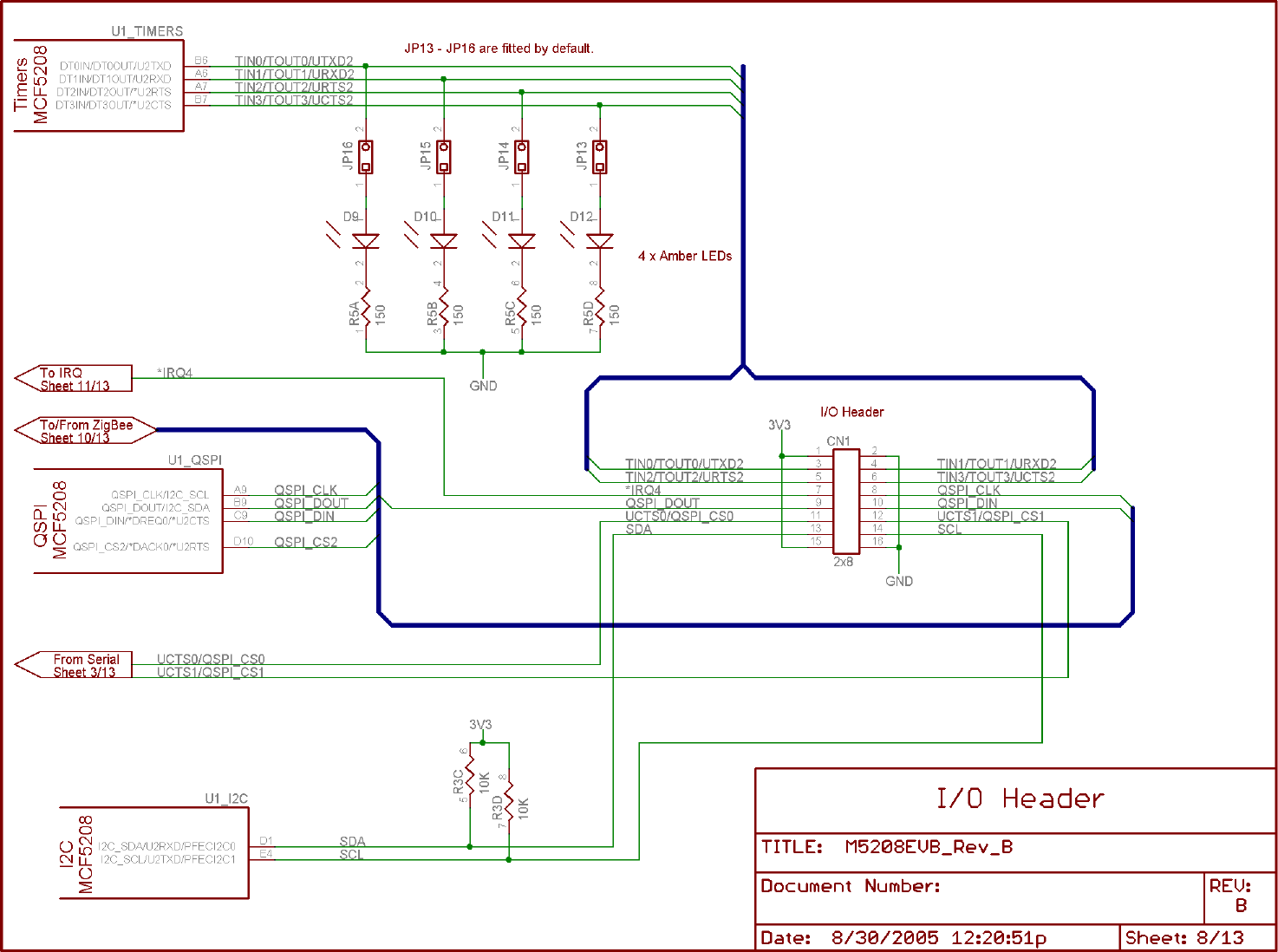
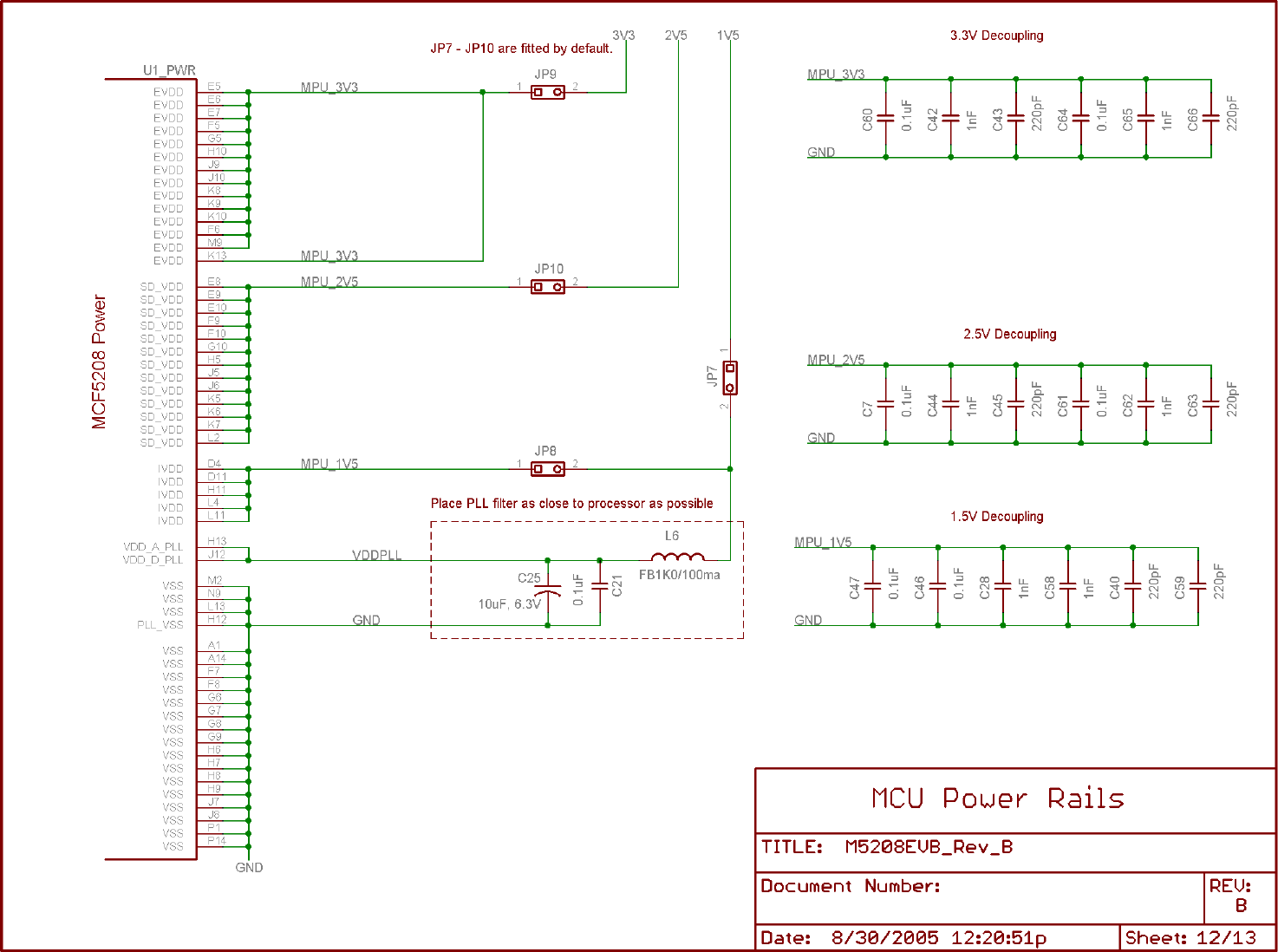
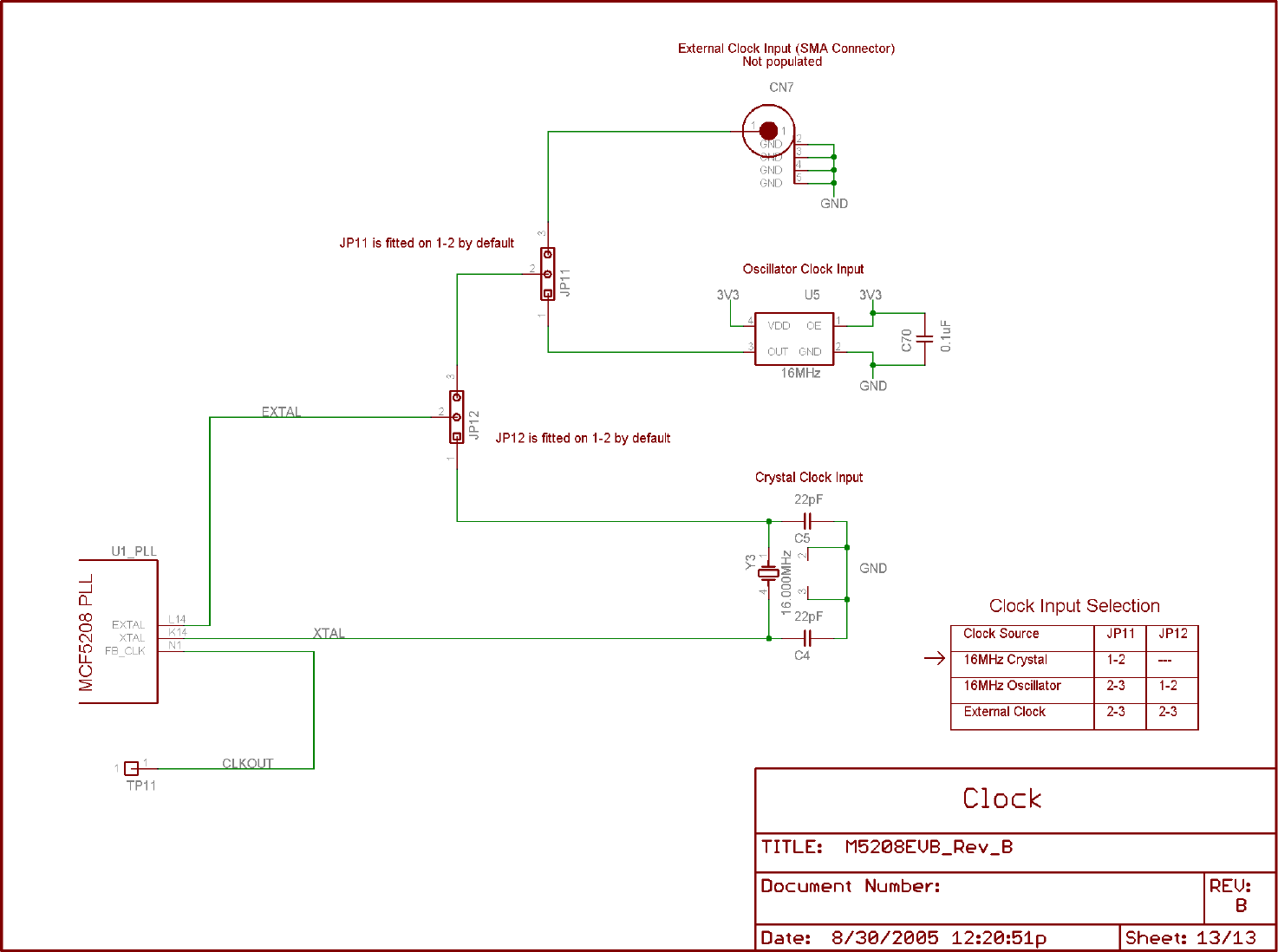
![JP3 – When fitted this jumper causes dBUG monitor to automatically load a program and run it. Typically this program is uClinux (as shipped). See Appendix C and the SBCTools Programmer Reference for more information on the Autorun feature of dBUG monitor. When this jumper is open, dBUG monitor will not run any user program and instead display the dBUG prompt on the terminal and wait for input. JP4 – When fitted this jumper disables the factory test mode of the MCF5208. This jumper is normally always fitted. JP5 – When fitted this jumper asserts the *RCON signal and causes the MCF5208 to load the CCR register based on the signals D9, D[7:1]. These signals are conditioned out of reset by the DIP switch. See the MCF5208 Reference Manual, (Ch 9 Chip Configuration Register) for more information on the reset configuration. JP6 – This jumper selects between DDR and SDR mode for the SDRAM module. Should always be fitted to support DDR mode. JP7 – When fitted connects 1.5V to the PLL filter and to JP8. JP8 – When fitted connects the processor core voltage to 1.5V. JP7 must also be fitted. JP9 – When fitted connects the processor I/O voltage to 3.3V. Also connects JP11 to 3.3V. JP10 – When fitted connects the processor external bus voltage to 2.5V. JP11 – This jumper selects between an external oscillator and an off-board frequency source. This jumper is only relevant is JP15 is in position 1-2. By default it is set to position 2-3 to JP12 – This jumper selects between the on board crystal or an external oscillator. It is in position 1-2 by default to select the on-board crystal. JP13 – This jumper connects TOUT3 to its LED. It is normally fitted. JP14 – This jumper connects TOUT2 to its LED. It is normally fitted. JP15 – This jumper connects TOUT1 to its LED. It is normally fitted. JP16 – This jumper connects TOUT0 to its LED. It is normally fitted. M5208EVBUM.pdf A - 3 1-Sep-05](https://usermanual.wiki/Intec-Automation/5208EVB/User-Guide-580592-Page-37.png)
![Switches Several switches on the M5208EVB are used to control the board’s configuration and operation. The switches are listed in Table A-2. Table A-2: Switch Functions Switches Function Power Switch Isolates M5208EVB from power supply. Reset Button Asserts the *RSTI signal forcing the MCF5208 and peripheral systems to reset. Abort Button Asserts the *IRQ7 signal causing an interrupt in the MCF5208. This interrupt is handled by dBUG monitor. Configuration Switch Determines the out of reset configuration of the MCF5208. Reset Configuration Switches The DIP switch on the M5208EVB determines the MCF5208’s personality out of reset when the *RCON signal is held low (JP5 is fitted). Table A-3: Reset Configuration Switch Functions SW1-1 PLL Mode OFF 166.67MHz Core bus, 83.33MHz External Bus operation ON 88MHz Core bus, 44MHz External Bus operation (Note 1) SW1-2 Oscillator Mode OFF Crystal oscillator mode ON Oscillator bypass mode SW1-3 SW1-4 Boot Port Size OFF OFF 16-bit port OFF ON 32-bit port ON OFF 32-bit port ON ON 8-bit port SW1-5 Output Pad Drive Strength OFF High drive strength ON Low drive strength SW1-6 LIMP Mode OFF Normal operation; PLL drives internal clocks. ON LIMP mode; low-power clock divider drives internal clocks. SW1-7 Oscillator Frequency Select OFF 16MHz is used as input to processor ON 16.67MHz is used as input to processor SW1-8 Chip Select Configuration OFF A[23:22] = A[23:22] ONN A[23:22] = *FB_CS[5:4] M5208EVBUM.pdf A - 4 1-Sep-05](https://usermanual.wiki/Intec-Automation/5208EVB/User-Guide-580592-Page-38.png)


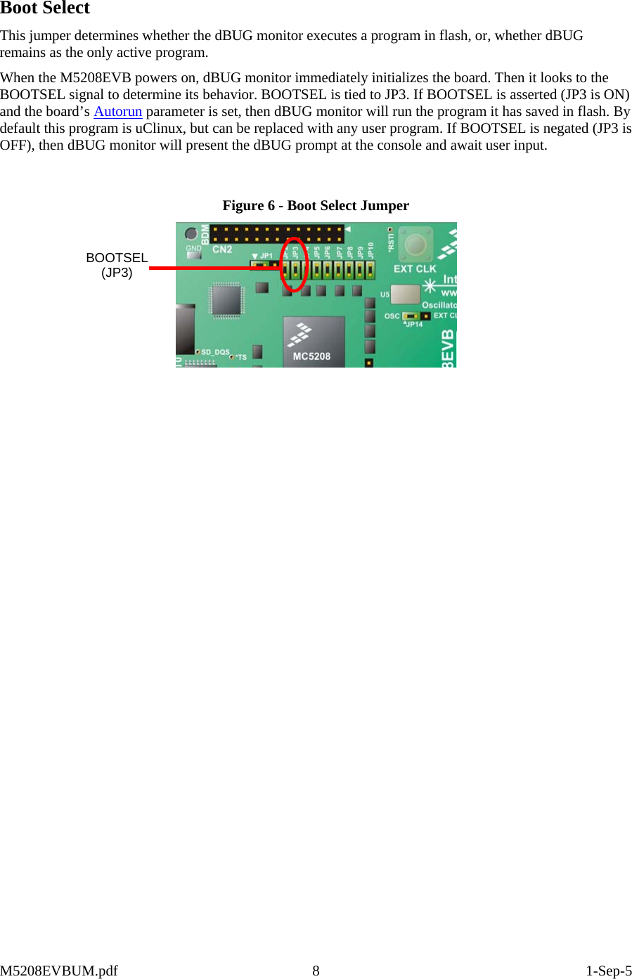
![dBUG and Autorun On startup, dBUG checks if JP3 is installed and if it is, then dBUG attempts to boot a program stored in external flash. A program can be stored into external flash by using the “dfl” or “dnfl” commands detailed below and in the dBUG user manual. The World as Seen by dBUG dBUG resides in the bottom 256K of the M5208EVB external flash. On startup, dBUG maps the 16MB SDRAM and accesses it as follows: • It sets up (DDR) SDRAM from 0x40000000 to 0x41FFFFFF. • It uses the lower 128K of SDRAM, that is, 0x40000000 to 0x4001FFFF for its vector table, data and stack. Consequently this memory space is out of bounds to the user program. • It expects the user program to always start at 0x40020000 in SDRAM. • A user program can use the MCF5208’s on-chip SRAM for stack space, since it is very fast and dBUG does not use this memory. Using dBUG Setting dBug Parameters dBUG stores several parameters on the SBC that determine dBUG’s behaviour. Resetting or repowering the board will not affect the values of these parameters: • Base -The numeral base used by dBUG for entry and display of all numbers [16]. • Baud - The baud rate shared by the SBC’s Primary and Secondary serial connection [115200]. Setting Board Parameters dBUG stores several parameters on the SBC that determine the SBC’s behavior. Resetting or repowering the board will not affect the values of these parameters. Some of these parameters are: • Watchdog - When On, the watchdog timer is left enabled on the MCF5208 and must be fed by the user program or the watchdog will reset the board after ~5 seconds. • Server - The IP address of a PC running a TFTP server. This setting is used for network downloads. • Client - The IP address of the board. • Gateway - The IP address of the gateway for the LAN that the board is connected to. • Netmask - The netmask of the LAN that the board is connected to. • DNS - The IP address of a DNS server, used for resolving a URL to IP address. • Ethaddr -The MAC address. dBUGmonitor.pdf C-2 5-Sep-05](https://usermanual.wiki/Intec-Automation/5208EVB/User-Guide-580592-Page-58.png)

![Useful uClinux Commands The following commands are widely used on all Linux based systems including uClinux. These are just a summary of useful commands; more documentation can be found for each of these commands at http://man.linuxquestions.org. Also typing “help” at the uClinux prompt “/>” will provide a complete listing of the command available. File System Manipulation • ls – list directory contents • cd – change directory • mkdir – make directory • rm – remove file • rmdir – remove directory • cp – copy a file • mv – move a file • cat - view a file on standard output • mount – mount a file system on top of a device o e.g.: />mount –t jffs2 /dev/mtdblock1 /mnt/flash • smbmount – mount a remote file share o e.g.: />smbmount //192.168.2.98/wokspace /mnt/workspace –o username=Mike,password=mike • sync – synchronize cached files in RAM to disk Network ifconfig The ifconfig command is used to view and edit network information such as IP address and subnet mask • ifconfig eth0 – display IP address and other network parameters • ifconfig eth0 [ip] netmask [netmask] – Set IP address to [ip] and netmask to [netmask] • ifconfig –h – display help on the ifconfig command uClinuxCommands.pdf C-1 5-Sep-05](https://usermanual.wiki/Intec-Automation/5208EVB/User-Guide-580592-Page-61.png)
![route The route command is used to view or edit network routing information. • route – display network routing table • route add default gw [gateway] – Add the default gateway to the routing table • route -h – diplay help for the route command mii-tool The mii-tool command is used to get and set low-level physical information from the network interface, such as speed and duplex. • mii-tool – display the physical Ethernet properties • mii-tool –v – display more information (verbose) • mii-tool –v –v – most verbose setting (includes raw dump of PHY chip registers in Hex) • mii-tool –restart – reset the physical Ethernet interface chip • mii-tool –h – help for the mii-tool command Date/Time date The date command will show or set the system date as kept by the kernel while running. This date will reset every time the board is rebooted. If you would like to keep the time accurate, you must use a battery backed RTC with the “hwclock” utility. • date – view the current system date • date [MMDDhhmm[YYYY]] – set the system date time System proc file system The proc file system provides diagnostics for the entire system. To view the diagnostics use the cat command in the /proc directory. • cat /proc/cpuinfo – displays stats about the CPU brand and speed • cat /proc/interrupts – statistics on interrupts • cat /proc/mounts – information on mounted filesystems uClinuxCommands.pdf C-2 5-Sep-05](https://usermanual.wiki/Intec-Automation/5208EVB/User-Guide-580592-Page-62.png)

![uClinux Device Drivers The following sections describe the various device drivers in uClinux that are importance to user application development. There are other drivers available in the /dev directory that are not included in this list because they are exclusively used by the kernel. ips (IPS) The “ips” driver has been developed by Intec to support the run time library under uClinux. The internal peripheral system (ips) driver provides user applications with access to the hardware registers. User applications should never use the ips driver directly, but instead simply call functions from the run time library provided. mtd[x]/mtdblock[x] (External Flash) The memory technology device (mtd) driver is for accessing the external flash device. On the Wildfire board this device provides access to the on board serial flash. To make use of the mtd driver a file system should be mounted on top of it. The Journaling Flash File System (JFFS2) is designed for these type of flash devices which require sector erases before writes. To use the mtd driver issue the following command at either the command line or from the rc file (done by default with the M5208EVB as shipped in the etc/rc file). 1. Create a directory if not already created (/>mkdir /mnt/flash) 2. Mount the file system (/>mount –t jffs2 /dev/mtdblock1 /mnt/flash) 3. To erase a device use the raw char driver (/>eraseall /dev/mtd1). This will erase all data on the device and is in fact like formatting the device. For the M5208EVB the partitions are as follows: 1. mtd0, mtdblock0 – 256K dBUG partition 2. mtd1, mtdblock1 – 640K JFFS2 partition 3. mtd2, mtdblock2 – 1152K compressed Kernel image Only the mtd1 partition should be used in most cases. Altering the other partitions could cause problems booting the board and will require the board to be re-flashed with the BDM pod. Once mounted the directory can be used like any other and will retain its data between power cycles. uClinuxDeviceDrivers.pdf D-1 27-Jun-05](https://usermanual.wiki/Intec-Automation/5208EVB/User-Guide-580592-Page-65.png)