Intel 82555 Users Manual 555ds_20
82555 i82555
82555 to the manual 99960140-d1dc-42a2-86f5-9a1ed2d89f60
2015-02-02
: Intel Intel-82555-Users-Manual-432686 intel-82555-users-manual-432686 intel pdf
Open the PDF directly: View PDF ![]() .
.
Page Count: 58
- 1.0 Introduction
- 2.0 Architectural Overview
- 3.0 Pin Definitions
- 4.0 100BASE-TX Adapter Mode Operation
- 5.0 10BASE-T Functionality in Adapter Mode
- 6.0 Repeater Mode
- 7.0 Management Data Interface
- 7.1 MDI Frame Structure
- 7.2 MDI Registers
- 7.2.1 MDI Registers 0 - 7
- 7.2.1.1 Register 0: Control Register Bit Definitions
- 7.2.1.2 Register 1: Status Register Bit Definitions
- 7.2.1.3 Register 2: 82555 Identifier Register Bit Definitions
- 7.2.1.4 Register 3: 82555 Identifier Register Bit Definitions
- 7.2.1.5 Register 4: Auto-Negotiation Advertisement Register Bit Definitions
- 7.2.1.6 Register 5: Auto-Negotiation Link Partner Ability Register Bit Definitions
- 7.2.1.7 Register 6: Auto-Negotiation Expansion Register Bit Definitions
- 7.2.2 MDI Registers 8 - 15
- 7.2.3 MDI Registers 16 - 31
- 7.2.3.1 Register 16: 82555 Status and Control Register Bit Definitions
- 7.2.3.2 Register 17: 82555 Special Control Bit Definitions
- 7.2.3.3 Register 20: 100BASE-TX Receive Disconnect Counter Bit Definitions
- 7.2.3.4 Register 21: 100BASE-TX Receive Error Frame Counter Bit Definitions
- 7.2.3.5 Register 22: Receive Symbol Error Counter Bit Definitions
- 7.2.3.6 Register 23: 100BASE-TX Receive Premature End of Frame Error Counter Bit Definitions
- 7.2.3.7 Register 24: 10BASE-T Receive End of Frame Error Counter Bit Definitions
- 7.2.3.8 Register 25: 10BASE-T Transmit Jabber Detect Counter Bit Definitions
- 7.2.3.9 Register 27: 82555 Special Control Bit Definitions
- 7.2.1 MDI Registers 0 - 7
- 8.0 Auto-Negotiation Functionality
- 9.0 LED Descriptions
- 10.0 Reset and Miscellaneous Test Modes
- 11.0 Electrical Specifications and Timing Parameters
- 11.1 Absolute Maximum Ratings
- 11.2 General Operating Conditions
- 11.3 DC Characteristics
- 11.4 AC Characteristics
- Figure 13. AC Testing Level Conditions
- 11.4.1 MII Clock Specifications
- 11.4.2 MII Timing Parameters
- 11.4.3 Repeater Mode Timing Parameters
- 11.4.4 Transmit Packet Timing Parameters
- 11.4.5 Squelch Test Timing Parameters
- 11.4.6 Jabber Timing Parameters
- 11.4.7 Receive Packet Timing Parameters
- 11.4.8 10BASE-T Normal Link Pulse (NLP) Timing Parameters
- 11.4.9 Auto-Negotiation Fast Link Pulse (FLP) Timing Parameters
- 11.4.10 Reset Timing Parameters
- 11.4.11 X1 Clock Specifications
- 11.4.12 100BASE-TX Transmitter AC Specification
- 12.0 82555 Package Information

82555 10/100 Mbps LAN Physical Layer
Interface
Networking Silicon
Datasheet
Product Features
■Optimal integration for lower cost solutions
—Integrated 10/100 Mbps single chip
physical layer interface solution
—Complete 10/100 Mbps MII compliance
with MDI support
—Full duplex operation in 10 Mbps and
100 Mbps modes
—IEEE 802.3u Auto-Negotiation support
for 10BASE-T half and full duplex,
100BASE-TX half and full duplex, and
100BASE-T4 configurations
—Parallel detection algorithm for legacy
support of non-Auto-Negotiation
enabled link partner
—Integrated 10BASE-T transceiver with
built in transmit and receive filters
—Glueless interface to T4-PHY for
combination TX/T4 designs with single
magnetics
—Glueless support for 4 LEDs: activity,
link, speed, and duplex
—LED function mapping support via MDI
—Low external component count
—Single 25 MHz clock support for 10
Mbps and 100 Mbps (crystal or
oscillator)
—Single magnetics for 10 Mbps and 100
Mbps operation
—QFP 100-pin package
■Performance enhancements
—Flow control support for IEEE 802.3x
Auto-Negotiation and Bay Technologies
PHY Base* scheme
—Adaptive Channel Equalizer for greater
functionality over varying cable lengths
—High tolerance to extreme noise
conditions
—Very low emissions
—Jabber control circuitry to prevent data
loss in 10 Mbps operation
—Auto-polarity correction for 10BASE-T
—Software compatible with 82557 drivers
■Repeater functionality
—Repeater mode operation
—Support for forced speed of 10 Mbps
and 100 Mbps
—Automatic carrier disconnect for IEEE
802.3u compliance
—Auto-Negotiation enable/disable
capability
—Receive port enable function
—Support for 32 configurable addresses
—Narrow analog side (14 mm) for tight
packing in repeater and switch designs
Document Number: 666252-004
Revision 2.0
March 1998
Notice:
Notice:

82555 — Networking Silicon
ii Datasheet
Revision History
■Low power consumption
—Typical total solution power including
all resistors and magnetics:
- 275 mA 100BASE-TX
- 230 mA 10BASE-T
- 250 mA Auto-Negotiation
—300 mA maximum total solution power
in DTE (adapter) mode
—Power-down of 10BASE-T/100BASE-
TX sections when not in use
■Added modes for design, testing, and
manufacturability
—Test Access Port (TAP)
- NAND Tree
- Board Level Functional Test (BIST)
—Programmable bypass for 4B/5B
encoding/decoding and scrambler/
descrambler
—Diagnostic loopback mode
Revision
Date Revision Description
Jan. 1997 1.0 First external release of the preliminary datasheet
Apr. 1997 1.1 First release edition
Mar. 1998 2.0 General editing
Information in this document is provided in connection with Intel products. No license, express or implied, by estoppel or otherwise, to any intellectual
property rights is granted by this document. Except as provided in Intel's Terms and Conditions of Sale for such products, Intel assumes no liability
whatsoever, and Intel disclaims any express or implied warranty, relating to sale and/or use of Intel products including liability or warranties relating to
fitness for a particular purpose, merchantability, or infringement of any patent, copyright or other intellectual property right. Intel products are not
intended for use in medical, life saving, or life sustaining applications.
Intel may make changes to specifications and product descriptions at any time, without notice.
Designers must not rely on the absence or characteristics of any features or instructions marked "reserved" or "undefined." Intel reserves these for
future definition and shall have no responsibility whatsoever for conflicts or incompatibilities arising from future changes to them.
The 82555 10/100 Mbps LAN Physical Layer Interface may contain design defects or errors known as errata which may cause the product to deviate
from published specifications. Current characterized errata are available on request.
Contact your local Intel sales office or your distributor to obtain the latest specifications and before placing your product order.
Copies of documents which have an ordering number and are referenced in this document, or other Intel literature, may be obtained from:
Intel Corporation
P.O. Box 7641
Mt. Prospect IL 60056-7641
or call 1-800-879-4683.
Copyright © Intel Corporation, 1997
*Third-party brands and names are the property of their respective owners.

Datasheet iii
Networking Silicon — 82555
Contents
1.0 INTRODUCTION..........................................................................................................................1
1.1 Functional Overview........................................................................................................1
1.2 Compliance to Industry Standards ..................................................................................1
2.0 ARCHITECTURAL OVERVIEW...................................................................................................3
2.1 100 Mbps Mode...............................................................................................................3
2.2 10 Mbps Mode.................................................................................................................4
2.3 Media Independent Interface (MII) ..................................................................................5
3.0 PIN DEFINITIONS........................................................................................................................7
3.1 Pin Types .......................................................................................................................8
3.2 Clock Pins ......................................................................................................................8
3.3 Twisted Pair Ethernet (TPE) Pins ...................................................................................8
3.4 Media Independent Interface (MII) Pins .........................................................................8
3.5 Media Access Control/Repeater Interface Control Pins .................................................9
3.6 LED Pins ......................................................................................................................10
3.7 External Bias Pins ........................................................................................................10
3.8 Miscellaneous Control Pins ..........................................................................................11
3.9 Power and Ground Pins ...............................................................................................12
4.0 100BASE-TX ADAPTER MODE OPERATION ..........................................................................13
4.1 100BASE-TX Transmit Clock Generation .....................................................................13
4.2 100BASE-TX Transmit Blocks ......................................................................................13
4.2.1 100BASE-TX 4B/5B Encoder ....................................................................13
4.2.2 100BASE-TX Scrambler and MLT-3 Encoder ...........................................14
4.2.3 100BASE-TX Transmit Framing ................................................................15
4.2.4 Transmit Driver ..........................................................................................16
4.3 100BASE-TX Receive Blocks .......................................................................................16
4.3.1 Adaptive Equalizer .....................................................................................17
4.3.2 Receive Clock and Data Recovery ............................................................17
4.3.3 MLT-3 Decoder, Descrambler, and Receive Digital Section......................17
4.3.4 100BASE-TX Receive Framing .................................................................17
4.3.5 100BASE-TX Receive Error Detection and Reporting...............................17
4.4 100BASE-TX Collision Detection ..................................................................................17
4.5 100BASE-TX Link Integrity and Auto-Negotiation Solution...........................................18
4.5.1 Link Integrity...............................................................................................18
4.5.2 Auto-Negotiation ........................................................................................18
4.5.3 Combination Tx/T4 Auto-Negotiation Solution...........................................18
4.6 Auto 10/100 Mbps Speed Selection ..............................................................................19
4.7 Adapter Mode Addresses..............................................................................................19
5.0 10BASE-T FUNCTIONALITY IN ADAPTER MODE ..................................................................21
5.1 10BASE-T Transmit Clock Generation..........................................................................21
5.2 10BASE-T Transmit Blocks...........................................................................................21
5.2.1 10BASE-T Manchester Encoder................................................................21
5.2.2 10BASE-T Driver and Filter .......................................................................21
5.3 10BASE-T Receive Blocks............................................................................................21
5.3.1 10BASE-T Manchester Decoder................................................................21
5.3.2 10BASE-T Twisted Pair Ethernet (TPE) Receive Buffer and Filter............21

82555 — Networking Silicon
iv Datasheet
Contents
5.3.3 10BASE-T Error Detection and Reporting .................................................22
5.4 10BASE-T Collision Detection.......................................................................................22
5.5 10BASE-T Link Integrity................................................................................................22
5.6 10BASE-T Jabber Control Function..............................................................................22
5.7 10BASE-T Full Duplex ..................................................................................................23
6.0 REPEATER MODE ....................................................................................................................25
6.1 Special Repeater Features............................................................................................25
6.2 Connectivity...................................................................................................................25
7.0 MANAGEMENT DATA INTERFACE..........................................................................................27
7.1 MDI Frame Structure..................................................................................................... 27
7.2 MDI Registers................................................................................................................28
7.2.1 MDI Registers 0 - 7.................................................................................... 28
7.2.2 MDI Registers 8 - 15.................................................................................. 31
7.2.3 MDI Registers 16 - 31................................................................................31
8.0 AUTO-NEGOTIATION FUNCTIONALITY.................................................................................. 35
8.1 Description ....................................................................................................................35
8.2 Parallel Detect and Auto-Negotiation ............................................................................36
9.0 LED DESCRIPTIONS ................................................................................................................39
10.0 RESET AND MISCELLANEOUS TEST MODES.......................................................................41
10.1 Reset.............................................................................................................................41
10.2 Loopback.......................................................................................................................41
10.3 Scrambler Bypass .........................................................................................................41
10.4 Test Port........................................................................................................................41
11.0 ELECTRICAL SPECIFICATIONS AND TIMING PARAMETERS .............................................. 43
11.1 Absolute Maximum Ratings ..........................................................................................43
11.2 General Operating Conditions ......................................................................................43
11.3 DC Characteristics ........................................................................................................43
11.3.1 MII DC Characteristics ..............................................................................43
11.3.2 10BASE-T Voltage/Current DC Characteristics ........................................43
11.3.3 100BASE-TX Voltage/Current DC Characteristics ................................... 44
11.4 AC Characteristics.........................................................................................................45
11.4.1 MII Clock Specifications.............................................................................45
11.4.2 MII Timing Parameters .............................................................................. 46
11.4.3 Repeater Mode Timing Parameters ..........................................................47
11.4.4 Transmit Packet Timing Parameters .........................................................48
11.4.5 Squelch Test Timing Parameters ..............................................................48
11.4.6 Jabber Timing Parameters ........................................................................49
11.4.7 Receive Packet Timing Parameters ..........................................................49
11.4.8 10BASE-T Normal Link Pulse (NLP) Timing Parameters .........................50
11.4.9 Auto-Negotiation Fast Link Pulse (FLP) Timing Parameters ....................50
11.4.10 Reset Timing Parameters .........................................................................51
11.4.11 X1 Clock Specifications ............................................................................51
11.4.12 100BASE-TX Transmitter AC Specification ..............................................52
12.0 82555 PACKAGE INFORMATION.............................................................................................53
Datasheet 1
Networking Silicon — 82555
1.0 Introduction
The 82555 is a highly integrated, physical layer interface solution designed for 10 and 100 Mbps
Ethernet systems based on the IEEE 10BASE-T and 100BASE-TX specifications. 100BASE-TX is
an IEEE 802.3 physical layer specification for use over two pairs of Category 5 unshielded twisted
pair or Type 1 shielded twisted pair cable. 100BASE-TX defines a signaling scheme not only for
100 Mbps, but also provides CSMA/CD compatibility with the 10 Mbps IEEE 802.3 10BASE-T
signaling standard.
1.1 Functional Overview
The 82555 is designed to work in two modes: Data Terminal Equipment (DTE) for adapters and
repeater for hubs and switches. When configured to DTE (adapter) mode, the 82555 incorporates
all active circuitry required to interface 10/100 Mbps Ethernet controllers and CSMA/CD MAC
components to 10 Mbps and 100 Mbps networks. In this and other documents the 82555 may be
referred to as the DTE, Physical Medium Device (PMD), or Physical Layer Medium (PLM). It
supports a direct glueless interface to Intel components such as the 82557 Fast Ethernet controller.
The 82555 also supports the Media Independent Interface (MII) signals as specified in the IEEE
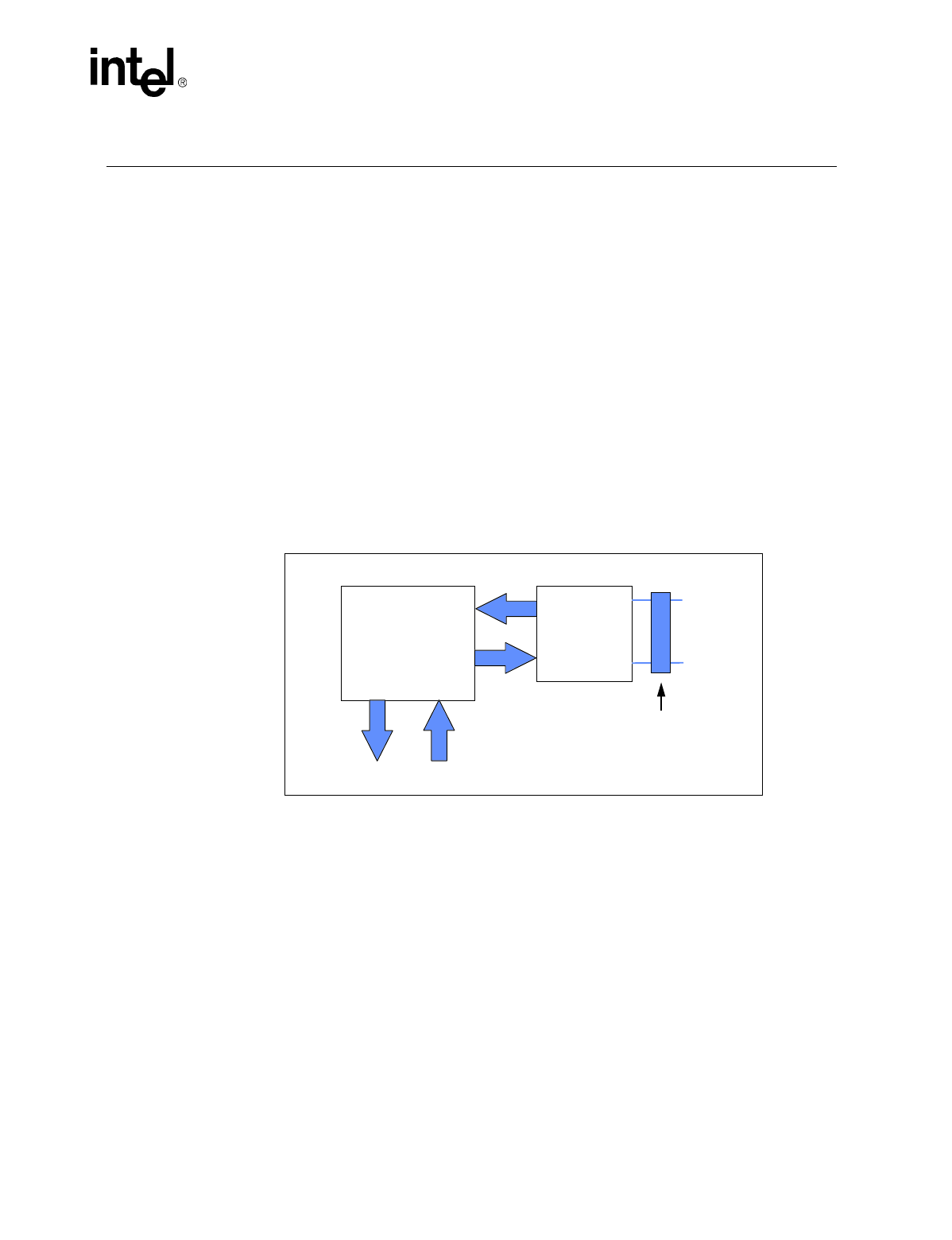
802.3u standard. The figure below shows how the 82555 fits into a 10/100 Mbps Ethernet adapter
design.
When configured to repeater mode, the 82555 incorporates several features that allow it to function
as a Class I or MII level repeater. Section 6.0, “Repeater Mode” on page 25 describes the 82555 in
a repeater type of application.
1.2 Compliance to Industry Standards
When operating in 100 Mbps mode, the 82555 complies with IEEE 802.3u 100BASE-TX
specification. The PMD section with the related changes established in 802.3u 100BASE-TX
complies with ANSI X3.263:1995 TP-PMD, Revision 2.2.
When operating in the 10 Mbps mode, the 82555 complies with the IEEE 802.3 10BASE-T
specification.
Figure 1. 82555 10/100 Mbps Ethernet Solution
Controller/MAC Intel 82555
System Bus Interface
Pair 1
Pair 2
Ma
g
netics

82555 — Networking Silicon
2 Datasheet
The 82555 also complies with the IEEE 802.3u Auto-Negotiation and the IEEE 802.3x Full Duplex
Flow Control sections. The MAC interface on the 82555 is a superset of the IEEE 802.3u Media
Independent Interface (MII) standard.
Datasheet 3
Networking Silicon — 82555
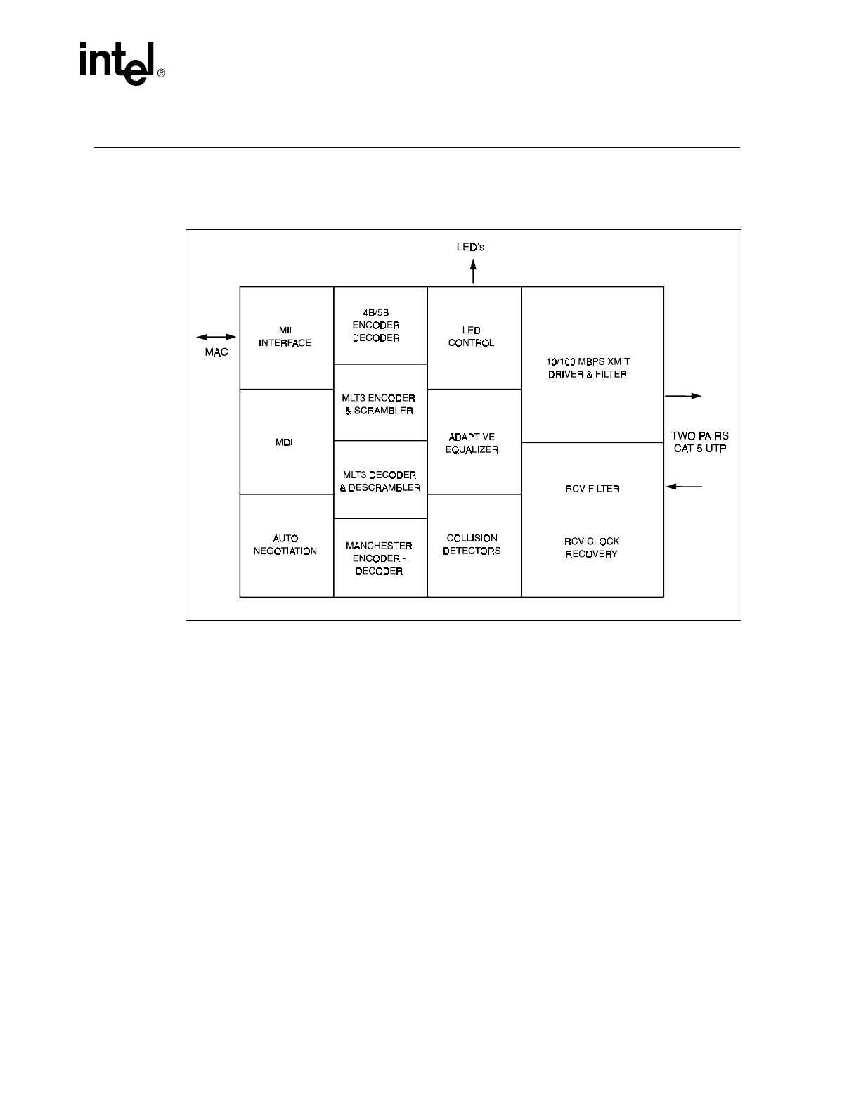
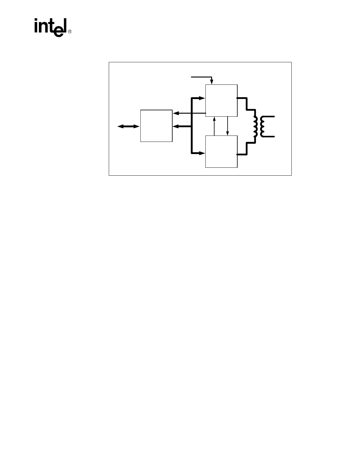
2.0 Architectural Overview
The 82555 is an advanced combination of both digital and analog logic which combine to provide a
functional stack between the Media Independent Interface (MII) and the wire through the
magnetics. Figure 2 shows a general block diagram of the 82555 component.
2.1 100 Mbps Mode
In 100BASE-TX mode the 82555 digital subsection performs all signal processing of digital data
obtained from the analog reception and the data to be driven into the analog transmit subsection.
This includes 4B/5B encoding/decoding, scrambling/descrambling, carrier sense, collision
detection, link detection, Auto-Negotiation, data validation, and providing MII to the Media
Access Controller (MAC). The 82555 supports the IEEE defined MII as its MAC interface and
expects the controller to drive the Management Data Input/Output and Management Data Clock
signals to perform the management functions.
In 100BASE-TX mode, the analog subsection of the 82555 performs two functions:
•Transmit: The 82555 converts a digital 125 Mbps stream into MLT-3 format and drives it
through the transmit differential pair onto the physical medium.
Figure 2. 82555 Simplified Block Diagram
82555 — Networking Silicon
4 Datasheet
•Receive: The 82555 takes receive analog MLT-3 data from the receive differential pair and
converts it into a digital 125 Mbps stream, recovering both clock and data signals.
2.2 10 Mbps Mode
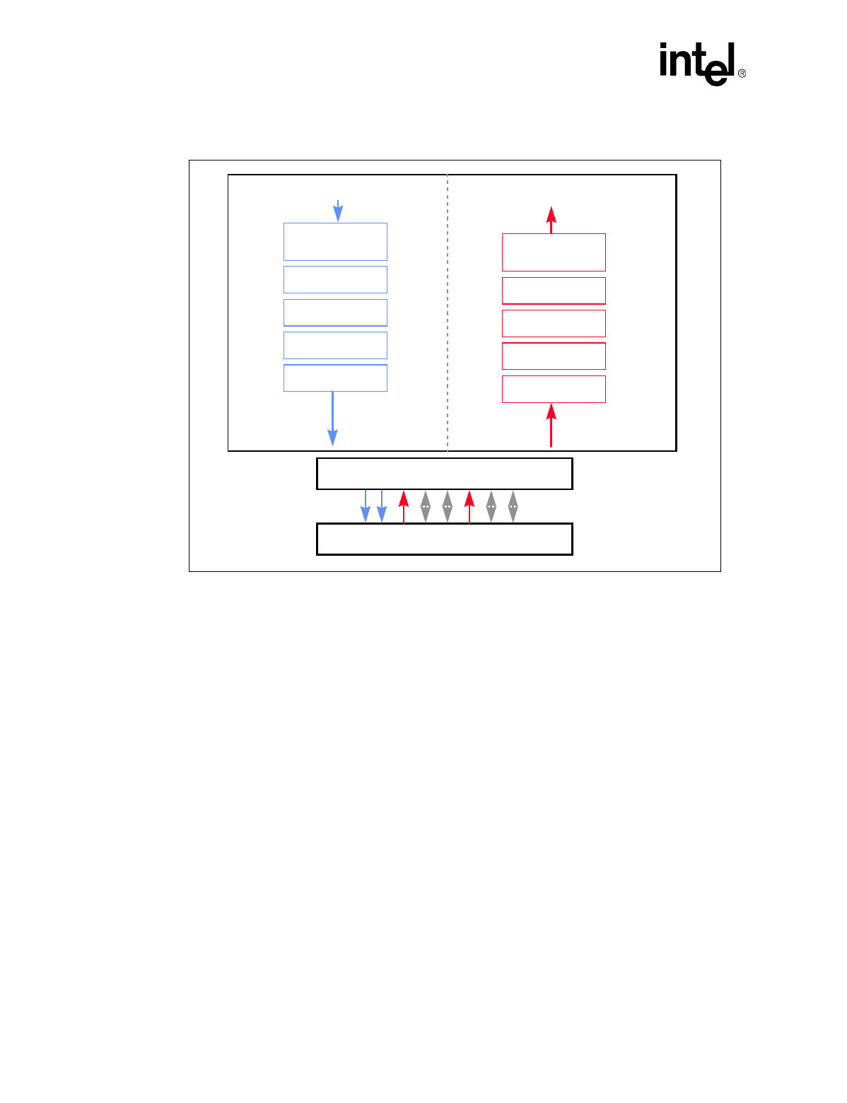
The 82555 operation in 10BASE-T mode is similar to the 82555 operation in 100BASE-TX mode.
Manchester encoding and decoding is used instead of 4B/5B encoding/decoding and scrambling/
descrambling. In addition, the Transmit Clock and Receive Clock (MII clock signals) provide 2.5
MHz instead of 25 MHz.
Figure 3. 82555 Analog Logic
4b/5b
Encoding
Scrambler
Serialization
MII TX Interface
NRZ to NRZI
NRZI to MLT3
4b/5b
Decoding
De-scrambler
Serial to 5B
MII RX Interface
NRZI to NRZ
MLT3 to NRZI
Magnetics Module
RJ-45 Connector
12345678
Datasheet 5
Networking Silicon — 82555
The 82555 provides a glueless interface to Intel components such as the 82557 Fast Ethernet
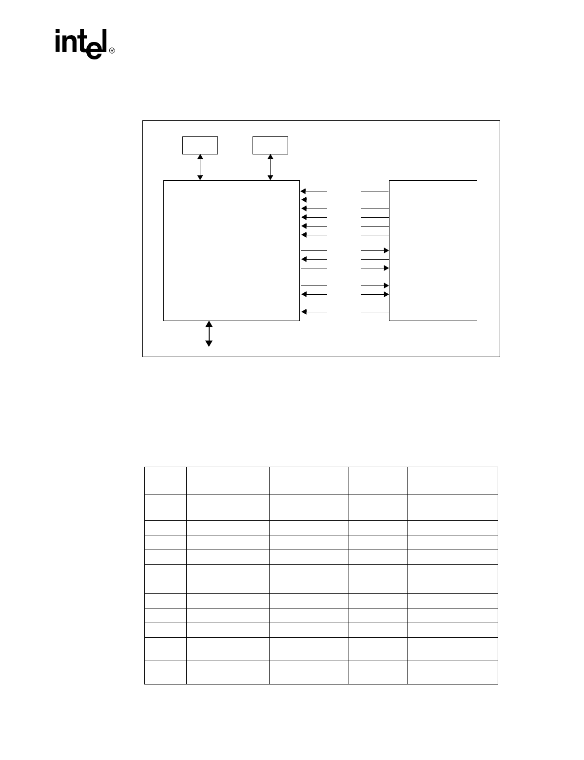
Controller, as well as any MII compatible device. Figure 4 shows a schematic-level diagram of the
82557 Fast Ethernet controller implementation connected to the 82555 using the MII interface.
2.3 Media Independent Interface (MII)
The 82555 supports the Media Independent Interface (MII) as its primary interface to the MAC.
The MII Interface is summarized in Table 1.
Figure 4. Intel 82557/82555 Solution
82557
Flash
(optional)
EEPROM
(
optional
)
PCI Bus Si
g
nals
82555
RXD[3:0]
RXC
RXERR
RXDV
CRS
COL
TXD[3:0]
TXC
TXEN
MDC
MDIO
RESET
Table 1. 82555 MII
Signal
Name Description Direction Clock
Reference MII Signal Supported
by the 82555?
TXC Transmit Clock From 82555
(adapter mode only) -- Yes
TXD[3:0] Transmit Data From MAC TXC Yes
TXEN Transmit Enable From MAC TXC Yes
COL Collision Detect From 82555 Asynchronous Yes
CRS Carrier Sense From 82555 Asynchronous Yes
RXC Receive Clock From 82555 -- Yes
RXD[3:0] Receive Data From 82555 RXC Yes
RXDV Receive Data Valid From 82555 RXC Yes
RXERR Receive Error From 82555 RXC Yes
MDC Management Data
Clock From manager -- Yes
MDIO Management Data
Input/Output From manager MDC Yes

82555 — Networking Silicon
6 Datasheet
TXERR Transmit Error
(repeater mode only) From RIC TXC Yes
Table 1. 82555 MII
Signal
Name Description Direction Clock
Reference MII Signal Supported
by the 82555?
Datasheet 7
Networking Silicon — 82555
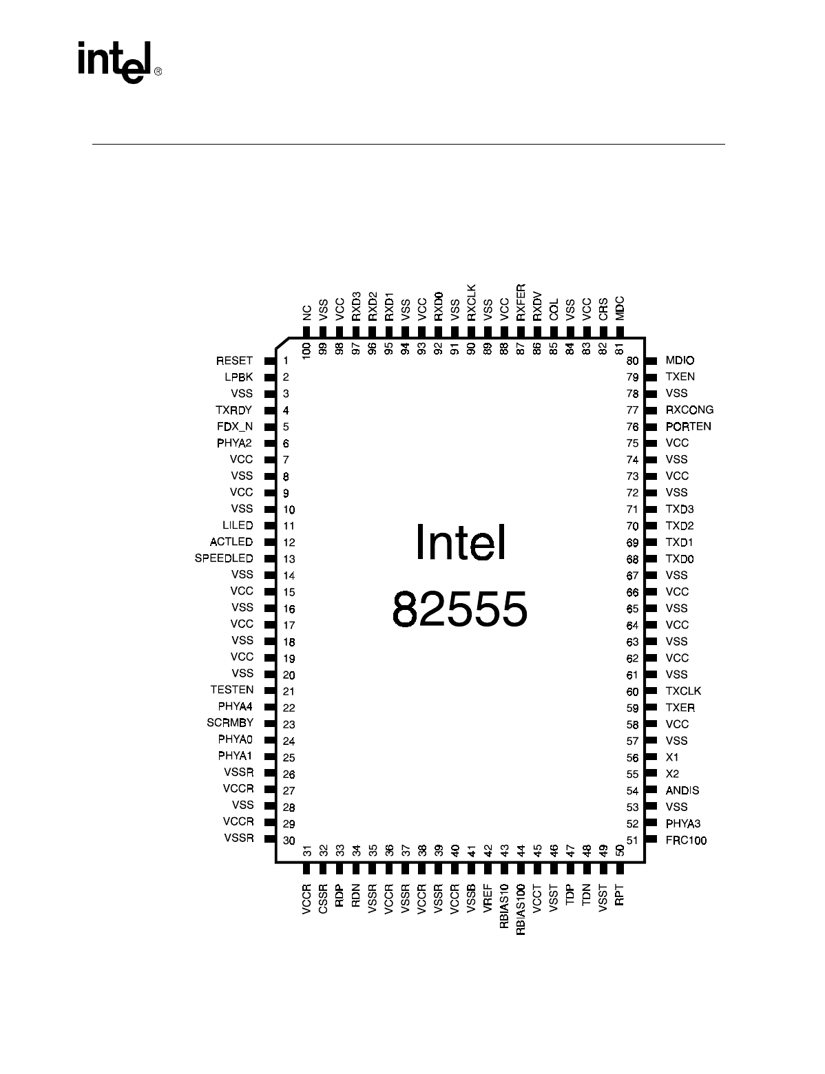
3.0 Pin Definitions
All active digital pins are defined to have transistor-to-transistor logic voltage levels except the X1
and X2 crystal signals. The transmit differential and receive differential pins are specified as analog
outputs and inputs, respectively.
The figure below show the pin locations on the 82555 component. The following subsections
describe the pin functions.
Figure 5. 82555 Pin Numbers and Labels

82555 — Networking Silicon
8 Datasheet
Pin allocation is based on a 100-lead quad flat package. All pin locations are based on printed
circuit board layout and other design constraints.
3.1 Pin Types
3.2 Clock Pins
3.3 Twisted Pair Ethernet (TPE) Pins
3.4 Media Independent Interface (MII) Pins
Pin Type Description
I This type of pin is an input pin to the 82555.
O This type of pin is an output pin from the 82555.
I/O This type of pin is both an input and output pin for the 82555.
B This pin is used as a bias pin. The bias pin is either pulled up or down with a resistor. The bias pin
may also be used as an external voltage reference.
Symbol Pin Type Name and Function
X1 56 I Crystal Input One. X1 and X2 can be driven by an external 25 MHz crystal.
Otherwise, X1 may be driven by an external MOS level 25 MHz oscillator
when X2 is left floating. (The crystal should have a tolerance of 50 PPM or
better.)
X2 55 O Crystal Output Two. X1 and X2 can be driven by an external 25 MHz
crystal. Otherwise, X1 may be driven by an external MOS level 25 MHz
oscillator when this pin is left floating.
Symbol Pin Type Name and Function
TDP
TDN
47
48
OTransmit Differential Pair. These pins send the serial bitstream for
transmission on an unshielded twisted pair (UTP) cable. The current-driven
differential driver can be two-level (10BASE-T or Manchester) or three-level
(100BASE-TX or MLT-3) signals depending on the operating mode. These
signals interface directly with an isolation transformer.
RDP
RDN
33
34
IReceive Differential Pair. These pins receive the serial bitstream from the
isolation transformer. The bitstream can be two-level (10BASE-T or
manchester) or three-level (100BASE-TX or MLT-3) signals depending on the
operating mode.
Symbol Pin Type Name and Function
RXD3
RXD2
RXD1
RXD0
97
96
95
92
OReceive Data. In 100 Mbps and 10 Mbps mode, data is transferred across
these four lines one nibble at a time.

Datasheet 9
Networking Silicon — 82555
3.5 Media Access Control/Repeater Interface Control Pins
RXC 90 O Receive Clock. The Receive Clock may be either 25 MHz or 2.5 MHz
depending on the 82555’s operating speed (25 MHz for 100 Mbps and 2.5
MHz for 10 Mbps). The Receive Clock is recovered directly from incoming
data and is continuous into the Media Access Controller (MAC). Thus, it must
be resynchronized in 10 Mbps mode at the start of each incoming packet.
RXDV 86 O Receive Data Valid. This signal indicates that the incoming data on the
RSC[3:0] pins are valid.
RXERR 87 O Receive Error. The RXERR signal indicates to the 82555 that an error has
occurred during frame reception.
TXD3
TXD2
TXD1
TXD0
71
70
69
68
ITransmit Data. In 100 Mbps and 10 Mbps mode, data is transferred across
these four lines one nibble at a time.
TXC 60 I/O Transmit Clock. The Transmit Clock may be either 25 MHz or 2.5 MHz
depending on the 82555’s operating speed (25 MHz for 100 Mbps and 2.5
MHz for 10 Mbps). The Transmit Clock outputs a continuous clock into the
MAC that is generated directly from the external clock source in DTE
(adapter) mode. In repeater mode, the TXC is an input signal operating at
either 25 MHz or 2.5 MHz depending on the operating speed, which is
typically clocked by a receiver interface device.
TXEN 79 I Transmit Enable. The Transmit Enable signal indicates to the 82555 that
valid data is present on the TXD[3:0] pins.
TXERR 59 I Transmit Error. The TXERR signal indicates to the 82555 that an error has
occurred during transmissions of a frame.
CRS 82 O Carrier Sense. The Carrier Sense signal indicates to the 82555 that traffic is
present on the link. CRS is an asynchronous output signal.
COL 85 O Collision Detect. The Collision Detect signal operates in half duplex mode
and indicates to the 82555 that a collision has occurred on the link. COL is an
asynchronous output signal to the controller.
MDIO 80 I/O Management Data Input/Output. The MDIO signal is a bidirectional data pin
for the Management Data Interface (MDI).
MDC 81 II Management Data Clock. The MDC signal functions as a clock reference for
the MDIO signal. MDC should operate at a maximum frequency of 2.5 MHz
Symbol Pin Type Name and Function
RXCONG 77 I Receive Congestion. If the following conditions exist, the RXCONG is an
active high and indicates an overrun on the controller receive side:
• Full duplex PHY Base (Bay Technologies) flow control DTE (adapter)
mode
• Full duplex signal (FDX_N) is high
• Full duplex technology is active through Auto-Negotiation
PORTEN 76 I Port Enable. In repeater mode when the PORTEN signal is low, the following
signals will be tri-stated: RXD[3:0], RXC, RXDV, and RXERR.
Symbol Pin Type Name and Function

82555 — Networking Silicon
10 Datasheet
3.6 LED Pins
3.7 External Bias Pins
Note: The resistor values described for the external bias pins are only recommended values and may
require to be fine tuned for various designs.
TXRDY
(TOUT)
4 O This pin is multiplexed and can be used for one of the following:
Transmit Ready. If full duplex and PHY Base (Bay Technologies) flow control
modes are enabled, the TXRDY signal enables transmission while it is
asserted.
TOUT. When the Test Enable signal is activated, this signal functions as the
Test Output port.
FDX_N 5 I/O Full Duplex. In DTE (adapter) mode, this active low output signal reports the
result of the duplex configuration to the MAC. This pin can also operate as
the LED driver and will be an active low for all technologies.
In repeater mode, this signal is used for Auto-Negotiation advertisement to
the 82555’s link partner and activates the PHY Base (Bay Technologies) flow
control if 100BASE-TX full duplex is the highest common technology between
the 82555 and its link partner.
Symbol Pin Type Name and Function
ACTLED 12 O Activity LED. This signal indicates either transmit or receive activity. When
activity is present, the ACTLED is on. When no activity is present, the
ACTLED is off.
LILED 11 O Link Integrity LED. This signal indicates the link integrity. If a valid link is
present in either 10 Mbps or 100 Mbps, the LILED is on; and if an invalid link
is preset, LILED is off.
For a combination design board, the LILED should be connected to the TX
technology LED.
SPEED-
LED 13 O Speed LED
This signal is used to indicate the speed of operation. For 100 Mbps, the
SPEEDLED will be on; and for 10 Mbps, the SPEEDLED will be off.
Symbol Pin Type Name and Function
RBIAS100 44 B Bias Reference Resistor 100. A 634 Ω resistor should be connected from
this pin to ground.
RBIAS10 43 B Bias Reference Resistor 10. A 768 Ω resistor should be connected from
this pin to ground.
PD1 42 I Pull Down One. A 10 KΩ resistor should be connected from this pin to
ground.
PD2 100 I Pull Down One. A 1 KΩ resistor should be connected from this pin to
ground.
Symbol Pin Type Name and Function

Datasheet 11
Networking Silicon — 82555
3.8 Miscellaneous Control Pins
Symbol Pin Type Name and Function
RESET 1 I Reset. The Reset signal is active high and resets the 82555. A reset pulse
width of at least 1 µs should be used.
FRC100
(MACTYP)
51 I This pin is multiplexed and can be used for one of the following:
Force 100/10 Mbps. In repeater mode, this pin configures the repeater to
either 100 Mbps (active high) or to 10 Mbps (active low).
MAC Type. In DTE (adapter) full duplex mode, if this input signal is high, the
82555 drives 82557 mode. If this input signal is low, the 82555 drives a
generic MII MAC mode.
PHYA4
(TIN)
22 I This pin is multiplexed and can be used for one of the following:
PHY Address 4. In repeater mode, this signal represents the fifth bit for
address port configuration.
TIN. If the Test Enable signal is active, this signal is used as the Test Input
data.
PHYA3
(SLVTRI)
52 I/O This pin is multiplexed and can be used for one of the following:
PHY Address 3. In repeater mode, this signal represents the fourth bit for
address port configuration.
Slave Tri-state. In DTE (adapter) mode, this output operates in conjunction
with the T4 Advanced signal. When both are active, the slave PHY is inactive
and tri-states all its outputs.
PHYA2
(LISTAT)
6 I This pin is multiplexed and can be used for one of the following:
PHY Address 2. In repeater mode, this signal represents the third bit for
address port configuration.
Link Status. In DTE (adapter) mode, if T4 Advance is active, the LISTAT_N
signal is active low and the slave PHY link is valid.
PHYA1
(TEXEC)
25 I This pin is multiplexed and can be used for one of the following:
PHY Address 1. In repeater mode, this signal represents the second bit for
address port configuration.
Test Execute. If Test Enable is asserted, this signal acts as the test
execution command indicating that the pin 22 is being used as the Test Input
pin.
PHYA0
(TCK)
24 I This pin is multiplexed and can be used for one of the following:
PHY Address 0. In repeater mode, this signal represents the first bit for
address port configuration.
Test Clock. If Test Enable is asserted, this signal acts as the Test Clock
signal.
ANDIS
(T4ADV)
54 I This pin is multiplexed and can be used for one of the following:
Auto-Negotiation Disable. In repeater mode, the Auto-Negotiation operates
for management reasons. If this input signal is high, the Auto-Negotiation
operation will be disabled.
T4ADV. In DTE (adapter) mode, this pin enables the combo mode. This
allows the LISTAT and SLVTRI pins to be used as interface to the slave PHY.
SCRMBY 23 I Scrambler/Descrambler Bypass. If SCRMBY is high, the scrambler/
descrambler of TP-PMD will be bypassed.
LPBK 2 I Loopback. When the LPBK signal is high, the 82555 will perform a
diagnostic loopback function.
RPT 50 I Repeater. When the RPT signal is high, the 82555 functions in repeater
mode. When this signal is low, the 82555 runs in DTE (adapter) mode.
TESTEN 21 I Test. If the TESTEN signal is high, the 82555 enables the test ports.

82555 — Networking Silicon
12 Datasheet
3.9 Power and Ground Pins
Symbol Pin Type Name and Function
VCC 7, 9, 15, 17, 19, 27, 29, 31, 36, 38, 40, 45, 58, 62,
64, 66, 73, 75, 83, 88, 93, 98 I Power: +5 V ± 5%
VSS 3, 8, 10, 14, 16, 18, 20, 26, 28, 30, 32, 35, 37, 39,
41, 46, 49, 53, 57, 61, 63, 65, 67, 72, 74, 78, 84, 89,
91, 94, 99
I Ground: 0 V

Datasheet 13
Networking Silicon — 82555
4.0 100BASE-TX Adapter Mode Operation
4.1 100BASE-TX Transmit Clock Generation
A 25 MHz crystal or a 25 MHz oscillator is used to drive the 82555’s X1 and X2 pins. The 82555
derives its internal transmit digital clocks from this crystal or oscillator input. The Transmit Clock
signal is a derivative of the 25 MHz internal clock. The accuracy of the external crystal or oscillator
must be ± 0.0005% (50 PPM).
4.2 100BASE-TX Transmit Blocks
The transmit subsection of the 82555 accepts nibble-wide data on the TXD[3:0] lines when TXEN
is asserted (high). The transmit subsection passes data unconditionally to the 4B/5B encoder as
long as TXEN is active.
The 4B/5B encoder accepts nibble-wide data (4 bits) from the MAC and compiles it into 5-bit-wide
parallel symbols. These symbols are scrambled and serialized into a 125 Mbps bit stream,
converted by the analog transmit driver into a MLT-3 waveform format, and transmitted onto the
Unshielded Twisted Pair (UTP) or Shielded Twisted Pair (STP) wire.
4.2.1 100BASE-TX 4B/5B Encoder
The 4B/5B encoder complies with the IEEE 802.3u 100BASE-TX standard. Four bits are encoded
according to the transmit 4B/5B lookup table. The lookup table matches a 5-bit code to each 4-bit
code.
The table below illustrates the 4B/5B encoding scheme associated with the given symbol.
Table 2. 4B/5B Encoder
Symbol 5B Symbol Code 4B Nibble Code
0 11110 0000
1 01001 0001
2 10100 0010
3 10101 0011
4 01010 0100
5 01011 0101
6 01110 0110
7 01111 0111
8 10010 1000
9 10011 1001
A 10110 1010
B 10111 1011
C 11010 1100
D 11011 1101

82555 — Networking Silicon
14 Datasheet
4.2.2 100BASE-TX Scrambler and MLT-3 Encoder
Data is scrambled in 100BASE-TX in order to reduce electromagnetic emissions during long
transmissions of high-frequency data codes. The scrambler logic accepts 5 bits from the 4B/5B
encoder block and presents the scrambled data to the MLT-3 encoder. The 82555 implements the
11-bit stream cipher scrambler as adopted by the ANSI XT3T9.5 committee for UTP operation.
The cipher equation used is:
X[n] = X[n-11] + X[n-9] (mod 2)
The MLT-3 encoder receives the scrambled Non-Return to Zero (NRZ) data stream from the
scrambler and encodes the stream into MLT-3 for presentation to the driver. MLT-3 is similar to
NRZI coding, but three levels are output instead of two. There are three output levels: positive,
negative and zero. When an NRZ “0” arrives at the input of the encoder, the last output level is
E 11100 1110
F 11101 1111
I 11111 Inter Packet Idle Symbol
(No 4B)
J 11000 1st Start of Packet Symbol
0101
K 10001 2nd Start of Packet Symbol
0101
T 01101 1st End of Packet Symbol
R 00111 2nd End of Packet Symbol
and Flow Control
V 00000 INVALID
V 00001 INVALID
V 00010 INVALID
V 00011 INVALID
H 00100 INVALID
V 00101 INVALID
V 00110 INVALID
V 01000 INVALID
V 01100 INVALID
V 10000 Flow Control S
V 11001 INVALID
Table 2. 4B/5B Encoder
Symbol 5B Symbol Code 4B Nibble Code
Datasheet 15
Networking Silicon — 82555
maintained (either positive, negative or zero). When an NRZ “1” arrives at the input of the encoder,
the output steps to the next level. The order of steps is negative-zero-positive-zero which continues
periodically. The figure below illustrates this process.
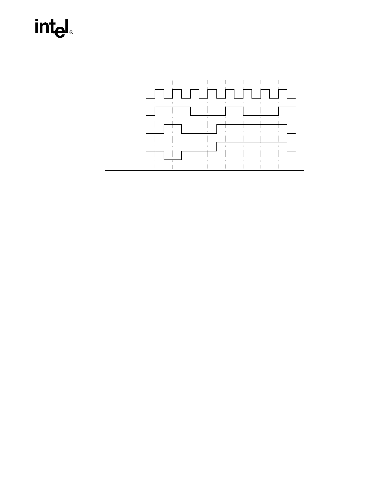
4.2.3 100BASE-TX Transmit Framing
The 82555 does not differentiate between the fields of the MAC frame containing preamble, start
of frame delimiter, data and Cyclic Redundancy Check (CRC). When TXEN is asserted, the 82555
accepts data on the MII TXD[3:0] lines, encodes it, and sends it out onto the wire. The 82555
encodes the first byte of the preamble as the “JK” symbol, encodes all other pieces of data
according to the 4B/5B lookup table, and adds the “TR” code after the end of the packet (de-
assertion of TXEN). The 82555 scrambles and serializes the data into a 125 Mbps stream, encodes
it as MLT-3, and drives it onto the wire. If TXERR is asserted during transmission of valid data, the
82555 transmits an invalid “H” symbol.
Figure 6. NRZ to MLT-3 Encoding Diagram
Clock
NRZ
NRZ1
MLT-3
1100 0110
1100 0110
1100 0110
82555 — Networking Silicon
16 Datasheet
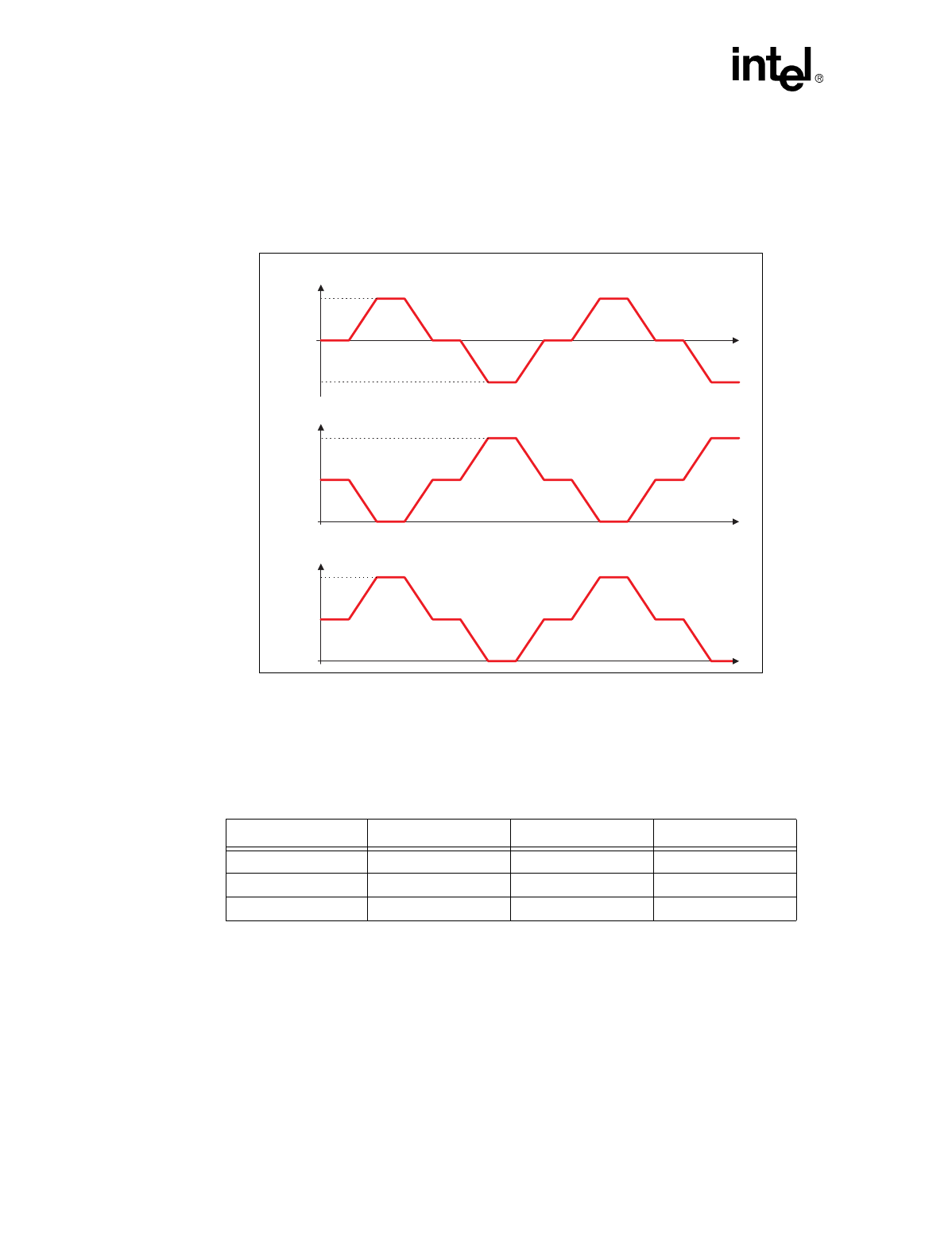
4.2.4 Transmit Driver
The transmit differential lines are implemented with a digital slope controlled current driver that
meets the TP-PMD specifications. Current is sunk from the isolation transformer by the transmit
differential pins. The conceptual transmit differential waveform for 100 Mbps is illustrated in the
following figure.
The magnetics module that is external to the 82555 converts ITDP and ITDN to 2.0 Vpp, as required
by the TP-PMD specification. The same magnetics used for 100BASE-TX mode should also work
in 10BASE-T mode. The following is a list of current magnetics modules available from several
vendors:
4.3 100BASE-TX Receive Blocks
The receive subsection of the 82555 accepts 100BASE-TX MLT-3 data on the receive differential
pair. Due to the advanced digital signal processing design techniques employed, the 82555 will
accurately receive valid data from Category 5 (CAT5) UTP and Type 1 STP cable of length well in
excess of 100 meters.
Figure 7. Conceptual Transmit Differential Waveform
(VTDP -VTDN )
+1V
0V
-1V
40mA
ITDP
20mA
0
40mA
20mA
0
ITDN
t
t
t
Table 3. Magnetics Modules
Vendor Model/Type 100BASE-TX 10BASE-T
Delta LF8200A Yes Yes
Pulse Engineering PE-68515 Yes Yes
Pulse Engineering H1012 Yes Yes

Datasheet 17
Networking Silicon — 82555
4.3.1 Adaptive Equalizer
The distorted MLT-3 signal at the end of the wire is restored by the equalizer. The equalizer
performs adaptation based on the shape of the received signal, equalizing the signal to meet
superior Data Dependent Jitter performance.
4.3.2 Receive Clock and Data Recovery
The clock recovery circuit uses advanced digital signal processing technology to compensate for
various signal jitter causes. The circuit recovers the 125 MHz clock and data and presents the data
to the MLT-3 decoder.
4.3.3 MLT-3 Decoder, Descrambler, and Receive Digital Section
The 82555 first decodes the MLT-3 data; afterwards, the descrambler reproduces the 5B symbols
originated in the transmitter. The descrambling is based on synchronization to the transmit 11-bit
Linear Feedback Shift Register (LFSR) during idle. The data is decoded at the 4B/5B decoder.
Once the 4B symbols are obtained, the 82555 outputs the receive data to the CSMA unit.
4.3.4 100BASE-TX Receive Framing
The 82555 does not differentiate between the fields of the MAC frame containing preamble, start
of frame delimiter, data and CRC. During 100 Mbps reception, the 82555 differentiates between
the idle condition ("L" symbols on the wire) and the preamble or start of frame delimiter. When
two non-consecutive bits are 0b within 10 bits (125 Mbps 5B data coding) the 82555 immediately
asserts the CRS signal. When the “JK” symbols (“11000, 10001”) are fully recognized, the 82555
asserts the RXDV signal and provides the data received on the MII RXD[3:0] to the Receive Clock.
If the “JK” symbol is not recognized (“false carrier sense”), the CRS signal is immediately de-
asserted and RXERR is asserted. Otherwise, the valid data is passed through the MII until the
82555 finds the “TR” (“01101, 00111”) and idle symbols in order to de-assert TXDV and CRS.
4.3.5 100BASE-TX Receive Error Detection and Reporting
In 100BASE-TX mode, the 82555 can detect errors in receive data in a number of ways. Any of the
following conditions is considered an error:
•Link integrity fails in the middle of frame reception.
•The start of stream delimiter “JK” symbol is not fully detected after idle.
•An invalid symbol is detected at the 4B/5B decoder.
•Idle is detected in the middle of a frame (before “TR” is detected).
When any of the above error conditions occurs, the 82555 immediately asserts the Receive Error
signal to the MAC. The RXERR signal is asserted as long as the receive error condition persists on
the receive pair.
4.4 100BASE-TX Collision Detection
100BASE-TX collisions in half duplex mode only are detected similarly to 10BASE-T collision
detection, via simultaneous transmission and reception.

82555 — Networking Silicon
18 Datasheet
4.5 100BASE-TX Link Integrity and Auto-Negotiation Solution
The 82555’s Auto-Negotiation function automatically configures the device to the technology,
media, and speed to operate with its link partner. Auto-Negotiation is widely described in IEEE
specification 802.3u, Clause 28. The 82555 supports 10BASE-T half duplex, 10BASE-T full
duplex, 100BASE-TX half duplex, and 100BASE-TX full duplex.
The 82555 has two Physical Medium Attachment (PMA) technologies with its link integrity
function, 10BASE-T and 100BASE-TX. The 82555 also has a special interface defined between
itself and a PHY-T4 in order to implement an Auto-Negotiation combination card.
4.5.1 Link Integrity
In 100BASE-TX, the link integrity function is determined by a stable signal status coming from the
TP-PMD block. Signal status is asserted when the PMD detects breaking squelch energy and the
right bit error rate according to the ANSI specification.
4.5.2 Auto-Negotiation
The 82555 fully supports IEEE 802.3u, Clause 28. In DTE (adapter) mode, the technology,
10BASE-T or 100BASE-TX, is determined by the Auto-Negotiation result. In repeater mode only,
this function can be disabled by pin configuration. If the T4ADV pin is active, the Auto-
Negotiation function will advertise and negotiate T4 technology.
Speed and duplex auto-select are functions of Auto-Negotiation. However, these parameters may
be manually configured via the MII management interface (MDI registers).
4.5.3 Combination Tx/T4 Auto-Negotiation Solution
The Auto-Negotiation function is available in both the 82555 and a PHY-T4. For these PHYs to
operate together, some arbitration at the PMA level is required and the Auto-Negotiation function
of one of the PHYs must be disabled. For this purpose, the 82555 is defined as the master; and the
PHY-T4, the slave. In combination mode, only the 82555’s Auto-Negotiation function is enabled
(the PHY-T4’s Auto-Negotiation is disabled).
In a combination board, a PHY-T4 is used only to support 100BASE-T4 operation and the 82555 is
sued to support 100BASE-TX full or half duplex and 10BASE-T full or half duplex as determined
by the Auto-Negotiation or Parallel Detection function.
Combination mode is available only in DTE (adapter) mode with the following pin interface:
•T4ADV (pin 54): Enables T4 technology in a PHY-TX Auto-Negotiation system.
•SLVTRI (pin 52): Disables the PHY-T4.The PHY-T4 is enabled only if the T4 technology has
been detected by Auto-Negotiation or Parallel Detection.
•LISTAT (pin 6): Indicates valid link on the PHY-T4. When SLVTRI is de-asserted, the PHY-
T4 should be active.
Datasheet 19
Networking Silicon — 82555
The figure below illustrates an 82557/82555/PHY-T4 solution in a block diagram.
4.6 Auto 10/100 Mbps Speed Selection
The MAC may either allow the 82555 to automatically select its operating speed or force the 82555
into 10 Mbps or 100 Mbps mode. The Management Data Interface (MDI) can control the 82555
speed mode.
The 82555 autoselect function determines the operation speed of the media based on the link
integrity pulses it receives. If no Fast Link Pulses (FLPs) are detected and Normal Link Pulses
(NLPs) are detected, the 82555 defaults to 10 Mbps operation. If the 82555 detects a speed change,
it dynamically changes its transmit clock and receive clock frequencies to the appropriate value.
This change takes a maximum of five milliseconds.
4.7 Adapter Mode Addresses
In DTE (adapter) mode, the 82555 supports addresses 0, 1, 2, and 3 through the pins PHYA1 and
PHYA0. Four addresses are sufficient in the case of a combination adapter having three PHYs. For
switch applications, the T4ADV signal should be de-asserted to allow all 32 addresses to be
available in repeater mode.
Figure 8. Combination Card Example
Common
Magnetics
PCI BUS
82557
fdx_n
PHY-T4
82555
T4
adv
MII
listat_n
slave_tri
3669

82555 — Networking Silicon
20 Datasheet

Datasheet 21
Networking Silicon — 82555
5.0 10BASE-T Functionality in Adapter Mode
5.1 10BASE-T Transmit Clock Generation
The 20 MHz and 10 MHz clocks needed for 10BASE-T are synthesized from the external 25 MHz
crystal or oscillator. The 82555 provides the transmit clock and receive clock to the MAC at 2.5
MHz.
5.2 10BASE-T Transmit Blocks
5.2.1 10BASE-T Manchester Encoder
After the 2.5 MHz clocked data is serialized in a 10 Mbps serial stream, the 20 MHz clock
performs the Manchester encoding. The Manchester code always has a mid-bit transition. If the
value is 1b then the transition is from low to high. If the value is 0b then the transition is from high
to low. The boundary transition occurs only when the data changes from bit to bit. For example, if
the value is 10b, then the change is from high to low; if 01b, then the change is from low to high.
5.2.2 10BASE-T Driver and Filter
Since 10BASE-T and 100BASE-TX have different filtration needs, both filters are implemented
inside the chip. This allows the two technologies to share the same magnetics. The 82555 supports
both technologies through one pair of transmit differential pins and by externally sharing the same
magnetics.
In 10 Mbps mode, the 82555 begins transmitting the serial Manchester bit stream within 3 bit times
(300 nanoseconds) after the MAC asserts TXEN. In 10 Mbps mode the line drivers use a pre-
distortion algorithm to improve jitter tolerance. The line drivers reduce their drive level during the
second half of “wide” (100 ns) Manchester pulses and maintain a full drive level during all narrow
(50 ns) pulses and the first half of the wide pulses. This reduces line overcharging during wide
pulses, a major source of jitter.
5.3 10BASE-T Receive Blocks
5.3.1 10BASE-T Manchester Decoder
The 82555 performs Manchester decoding and timing recovery when in 10 Mbps mode. The
Manchester encoded data stream is decoded from the receive differential pair to separate Receive
Clock and Receive Data lines from the differential signal. This data is transferred to the controller
at 2.5 MHz/nibble through the MII. The high-performance circuitry of the 82555 exceeds the IEEE
802.3 jitter requirements.
5.3.2 10BASE-T Twisted Pair Ethernet (TPE) Receive Buffer and Filter
In 10 Mbps mode, data is expected to be received on the receive differential pair after passing
through isolation transformers. The filter is implemented inside the 82555 for supporting single
magnetics that are shared with the 100BASE-TX side. The input differential voltage range for the

82555 — Networking Silicon
22 Datasheet
Twisted Pair Ethernet (TPE) receiver is greater than 585 mV and less than 3.1 V. The TPE receive
buffer distinguishes valid receive data, link test pulses, and the idle condition, according to the
requirements of the 10BASE-T standard.
The following line activity is determined to be inactive and is rejected:
•Differential pulses of peak magnitude less than 300 mV.
•Continuous sinusoids with a differential amplitude less than 6.2 Vpp and frequency less than 2
MHz.
•Sine waves of a single cycle duration starting with 0° or 180° phase that have a differential
amplitude less than 6.2 Vpp and a frequency of at least 2 MHz and not more than 16 MHz.
These single-cycle sine waves are discarded only if they are preceded by 4 bit times (400
nanoseconds) of silence.
All other activity is determined to be either data, link test pulses, Auto-Negotiation fast link pulses,
or the idle condition. When activity is detected, the carrier sense signal is asserted to the MAC.
5.3.3 10BASE-T Error Detection and Reporting
In 10 Mbps mode, the 82555 can detect errors in the receive data. The following condition is
considered an error:
The receive pair’s voltage level drops to the idle state during reception before the end-of-frame
bit is detected (250 nanoseconds without mid-bit transitions).
5.4 10BASE-T Collision Detection
Collision detection in 10 Mbps mode is indicated by simultaneous transmission and reception. If
the 82555 detects this condition, it asserts a collision indication to the controller.
5.5 10BASE-T Link Integrity
The link integrity in 10 Mbps works with link pulses. The 82555 senses and differentiates those
link pulses from fast link pulses and from 100BASE-TX idles. In the first and last case, the 82555
activates parallel detection of the respective technology; and in the second case, Auto-Negotiation.
The 10 Mbps link pulses or normal link pulses are driven in the transmit differential pair line but
are 100 ns wide and have levels from 0 V to 5 V. The link beat pulse is also used to determine if the
receive pair polarity is reversed. If it is, the polarity is corrected internally.
5.6 10BASE-T Jabber Control Function
The 82555 contains a jabber control function that inhibits transmission after a specified time
window when enabled. In 10 Mbps mode, the jabber timer is set to a value between 26.2 ms and 39
ms. If the 82555 detects continuous transmission that is greater than this time period, it prevents
further transmissions from onto the wire until it detects that the MAC transmit enable signal has
been inactive for at least 314 ms.

Datasheet 23
Networking Silicon — 82555
5.7 10BASE-T Full Duplex
The 82555 supports 10 Mbps full duplex by disabling the collision function, the squelch test, and
the carrier sense transmit function. This allows the 82555 to transmit and receive simultaneously,
achieving up to 20 Mbps of network bandwidth. The configuration can be achieved through Auto-
Negotiation. Full duplex should only be used in point-to-point connections (no shared media).
Flow control is always disabled.

82555 — Networking Silicon
24 Datasheet

Datasheet 25
Networking Silicon — 82555
6.0 Repeater Mode
The 82555 has a compete set of repeater features making it the ideal PHY for Class 1 (MII)
repeater designs. The 82555 works in repeater mode when the RPT signal (pin 50) is high. The
FRC100 signal (pin 51) determines which type of repeater is supported, either 100BASE-TX or
10BASE-T.
6.1 Special Repeater Features
Special features of the 82555 repeater mode operation include:
•Fully IEEE compliant with automatic carrier disconnect.
The 82555 will disconnect when it receives false carrier detects. Either a long series of valid
idle symbols or a valid “JK” pair will cause it to reconnect.
•Narrow 14 mm analog side that enables tight packing of multiple PHYs, which is ideal for 8,
12, 18, 24, or even 32 port repeater designs.
•Very low emissions and high noise immunity.
•32 configurable addresses through five address lines.
•Auto-Negotiation disable function.
In repeater mode, the Auto-Negotiation function is not used for configuration purposes. When
Auto-Negotiation is enabled in repeater mode, the MII management will be able to obtain data
from the MDI Auto-Negotiation register about the remote partner. This is a feature for hub
management allowing a 10/100 Mbps repeater design to automatically detect whether or not it
can operate at 100 Mbps. If the ANDIS signal is de-asserted, the Auto-Negotiation feature will
be disabled.
•Forced 10 Mbps or 100 Mbps operation (allows for a 10/100 repeater design).
•Receive port enable function.
The PORTEN signal is a glueless interface to the Repeater Interface Controller (RIC). When
the PORTEN signal is low, all receive signals are tri-stated, except CRS and COL.
•26-bit PHY budget for round trip.
The total PHY bit budget is 8 bits from the MII to the wire and 18 bits from the wire to the
MII.
•Static 2.5 MHz (10BASE-T) or 25 MHz (100BASE-TX) clock input for repeater designs
(issued by RIC).
The 82555 clock source is fixed between Resets. There is one input, either 2.5 MHz or 25
MHz, as indicated by the level at the FRC100 pin. All clocks have a common source
generation so the that PPM is 0 between them (X1, 2.5 MHz and 25 MHz).
•DTE (adapter) features not available in repeater mode: full duplex, flow control, and the
combination Auto-Negotiation interface for T4.
6.2 Connectivity
A 25 MHz buffered oscillator can provide the clock to all of the 82555 devices. A 2.5 MHz (10
Mbps) or a 25 MHz (100 Mbps) signal is required to clock the RIC and the TXC signal in the
PHYs. TXD[3:0], TXERR, RXC, RXD[3:0], RXDV, and RXERR are single-bus (shortened) for all

82555 — Networking Silicon
26 Datasheet
PHYs connected to the RIC. Signals TXEN, CRS, and PORTEN are connected from each of the
82555 devices to the specified RIC pin. The figure below illustrates an example of multiple 82555s
connected to a 25 MHz (or 2.5 MHz) oscillator.
Figure 9. Clock Signal Example
X1
TXCLK
CLK
RIC
PHY1 PHY2 PHY3
X1 X1
TXCLK TXCLK
PC-3691
2.5/25 MHz (10/100)
2.5/25 MHz (10/100)

Datasheet 27
Networking Silicon — 82555
7.0 Management Data Interface
The 82555 provides status and accepts management information through the Management Data
Interface (MDI). This is accomplished through read and write operations to various registers in
accordance with the IEEE 802.3u MII specification.
7.1 MDI Frame Structure
Data read from or written to a particular register is called a management frame and is sent serially
over the MDIO pin synchronously to the MDC signal. Read and write cycles are viewed from the
perspective of the controller. Thus, the controller always drives the start, opcode, PHY address, and
register address onto the MDIO pin. For read cycles, the controller drives the transition bits and
data onto the MDIO pin; for write cycles, to the 82555. The controller drives addresses and data on
the falling edge of the MDC signal, and the 82555 latches the data on the rising edge of the MDC
signal. The following list defines protocol terms:
PREAMBLE At the beginning of each transaction, the controller send a sequence of 32
contiguous logic one bits on the MDIO pin with corresponding cycles on the MDC
pin for synchronization by the 82555.
ST This field contains the value of 01b indicating the start of a frame.
OP This is a 2-bit field containing one of the following two operation codes: 10b (read)
or 01b (write).
PHYAD This field is a 5-bit address of the 82555 device that provides support for 32 unique
PHY addresses. The controller drives the value written into the PHYAD portion of
the MDI register in this field.
REGAD This field is a 5-bit address of a specific register within the 82555. This provides
support for 32 unique registers. The desired register address is specified by the
value written to the MDI register.
TA This field contains a 2-bit value specifying the period during a read cycle that no
device may actively drive the MDIO signal. During a read transaction, the 82555
should not drive the MDIO signal in the first bit time; however, it will drive a 0b in
the second bit time. During a write transaction, the controller drives the pattern of
10b to fill this time.
DATA This field contains 16 bits of data driven by the 82555 on a read transaction or by
the controller on a write transactions. This data is either control or status parameters
passed between the controller and the 82555.
IDLE During the idle state, the MDIO signal is in a high impedance state. The MDIO
driver is disabled, and the 82555 will pull the MDIO signal high to a logic 1.

82555 — Networking Silicon
28 Datasheet
The 82555 address can be configured to four 0 through 3 in DTE (adapter) mode and 0 through 31
in repeater mode. A special functions for switches allows 32 addresses to exist in repeater mode.
The management frame structure is as follows:
7.2 MDI Registers
MDI registers are described in the following subsections and the acronyms mentioned in the
registers are defined as follows:
SC - Self Cleared.
RO -Read Only.
P- External pin affects 82555 register content.
LL - Latch Low.
LH - Latch High.
7.2.1 MDI Registers 0 - 7
7.2.1.1 Register 0: Control Register Bit Definitions
Transition ST OP PHYAD REGAD TA DATA
READ <01> <10> <AAAAA> <RRRRR> <
X
0> 16 bits
WRITE <01> <01> <AAAAA> <RRRRR> <10> 16 bits
Bit(s) Name Description Default R/W
15 Reset This bit sets the status and control register of the 82555
to their default states and is self-clearing. The PHY
returns a value of 1b until the reset process has
completed and accepts a read or write transaction.
1 = PHY Reset
0 = Normal operation
0RW
SC
14 Loopback This bit enables loopback of transmit data nibbles from
the TXD[3:0] signals to the receive data path. The
82555’s receive circuitry is isolated from the network.
Note that this may cause the descrambler to lose
synchronization and produce 560 nanoseconds of “dead
time.”
Note also that the loopback configuration bit takes priority
over the Loopback MDI bit.
1 = Loopback enabled
0 = Loopback disabled (normal operation)
0RW
P
13 Speed Selection This bit controls speed when Auto-Negotiation is disabled
and is valid on read when Auto-Negotiation is disabled.
1 = 100 Mbps
0 = 10 Mbps
1RW
P
12 Auto-Negotiation
Enable This bit enables Auto-Negotiation. Bits 13 and 8, Speed
Selection and Duplex Mode, respectively, are ignored
when Auto-Negotiation is enabled.
1 = Auto-Negotiation enabled
0 = Auto-Negotiation disabled
1RW

Datasheet 29
Networking Silicon — 82555
7.2.1.2 Register 1: Status Register Bit Definitions
11 Power-Down This bit sets the 82555 into a low power mode.
1 = Power-down enabled
0 = Power-down disabled (normal operation)
0RW
10 Isolate This bit allows the 82555 to electrically isolate the Media
Independent Interface. When the MII is isolated, the
82555 does not respond to TXD[3:0], TXEN, and TXERR
input signals. Also, the 82555 presents high impedance
on its TXC, RXC, RXDV, RXERR, RXD[3:0], COL, and
CRS output signals. In the TX mode, the 82555 responds
to management transactions.
1 = Electrically isolate MII
0 = Normal operation
0RW
9 Restart Auto-
Negotiation This bit restarts the Auto-Negotiation process and is self-
clearing.
1 = Restart Auto-Negotiation process
0 = Normal operation
0RW
SC
8 Duplex Mode This bit controls the duplex mode when Auto-Negotiation
is disabled. If the 82555 reports that it is only able to
operate in one duplex mode, the value of this bit shall
correspond to the mode which the 82555 can operate.
When the 82555 is placed in Loopback mode, the
behavior of the PHY shall not be affected by the status of
this bit, bit 8.
1 = Full Duplex
0 = Half Duplex
0RW
7 Collision Test This bit will force a collision in response to the assertion
of the transmit enable signal.
1 = Force COL
0 = Do not force COL
0RW
6:0 Reserved These bits are reserved and should be set to 0000000b. 0 RW
Bit(s) Name Description Default R/W
15 100BASE-T4 1 = 82555 able to perform 100BASE-T4
0 = 82555 not able to perform 100BASE-T4
-- RO
P
14 100BASE-TX Full
Duplex 1 = 82555 able to perform full duplex 100BASE-TX
0 = 82555 not able to perform full duplex in repeater
mode
-- RO
P
13 100 Mbps Half
Duplex 1 = 82555 able to perform half duplex 100BASE-TX
0 = 82555 not able to perform 100BASE-TX
-- RO
P
12 10 Mbps Full
Duplex 1 = 82555 able to operate at 10 Mbps in full duplex
mode
0 = 82555 not able to operate in full duplex mode in
10BASE-T
-- RO
P
11 10 Mbps Half
Duplex 1 = 82555 able to operate at 10 Mbps in half duplex
mode
0 = 82555 not able to operate in 10BASE-T
-- RO
P
10:7 Reserved These bits are reserved and should be set to 0000b. 0 RO
Bit(s) Name Description Default R/W

82555 — Networking Silicon
30 Datasheet
7.2.1.3 Register 2: 82555 Identifier Register Bit Definitions
7.2.1.4 Register 3: 82555 Identifier Register Bit Definitions
7.2.1.5 Register 4: Auto-Negotiation Advertisement Register Bit Definitions
6 Management
Frames Preamble
Suppression
1 = 82555 will accept management frames with
preamble suppressed
0 = 82555 will not accept management frames with
preamble suppressed
-- RO
5 Auto-Negotiation
Complete 1 = Auto-Negotiation process completed
0 = Auto-Negotiation process has not completed
0RO
4 Remote Fault 1 = Remote fault condition detected
0 = No remote fault condition detected
0RO
P
3 Auto-Negotiation
Ability 1 = 82555 is able to perform Auto-Negotiation
0 = 82555 is in repeater mode and Auto-Negotiation
Disable pin is high
1RO
2 Link Status 1 = Valid link has been established
0 = Invalid link detected
0RO
LL
SC
1 Jabber Detect 1 = Jabber condition detected
0 = No jabber condition detected
0RO
LH
SC
0 Extended
Capability 1 = Extended register capabilities enabled
0 = No extended register capabilities
1RO
Bit(s) Name Description Default R/W
15:0 82555 ID (high
byte) Value: 02A8H -- RO
Bit(s) Name Description Default R/W
15:0 82555 ID (low
byte) Value: 0150H -- RO
Bit(s) Name Description Default R/W
15 Next Page Constant 0 = Transmitting primary capability data
page -- RO
14 Reserved This bit is reserved and should be set to 0b. 0 RO
13 Remote Fault 1 = Indicate link partner’s remote fault
0 = No remote fault
0RW
12:5 Technology Ability
Field Technology Ability Field is an 8-bit field containing
information indicating supported technologies specific
to the selector field value.
-- RW
4:0 Selector Field The Selector Field is a 5-bit field identifying the type of
message to be sent via Auto-Negotiation. This field is
read only in the 82555 and contains a value of
00001b, IEEE Standard 802.3.
00001 RO
Bit(s) Name Description Default R/W

Datasheet 31
Networking Silicon — 82555
7.2.1.6 Register 5: Auto-Negotiation Link Partner Ability Register Bit Definitions
7.2.1.7 Register 6: Auto-Negotiation Expansion Register Bit Definitions
7.2.2 MDI Registers 8 - 15
Registers eight through fifteen are reserved for IEEE.
7.2.3 MDI Registers 16 - 31
Register numbers 16, 17, 20, 21, 22, 23, 24, 25, and 27 are described in the following subsections.
Bit(s) Name Description Default R/W
15 Next Page This bit reflects the 82555’s link partner’s Auto-
Negotiation ability. -- RO
14 Acknowledge This bit is used to indicate that the 82555 has
successfully received its link partner’s Auto-
Negotiation advertising ability.
-- RO
13 Remote Fault This bit reflects the 82555’s link partner’s Auto-
Negotiation ability. -- RO
12:5 Technology Ability
Field This bit reflects the 82555’s link partner’s Auto-
Negotiation ability. -- RO
4:0 Selector Field This bit reflects the 82555’s link partner’s Auto-
Negotiation ability. -- RO
Bit(s) Name Description Default R/W
15:5 Reserved These bits are reserved and should be set to a
constant 0. 0RO
4 Parallel Detection
Fault 1 = Fault detected via parallel detection (multiple link
fault occurred)
0 = No fault detected via parallel detection
This bit will self-clear on read
0RO
SC
LH
3 Link Partner Next
page Able 1 = Link Partner is Next Page able
0 = Link Partner is not Next Page able
0RO
2 Next Page Able 1 = Local drive is Next Page able
0 = Local drive is not Next Page able
0RO
1 Page Received 1 = New Page received
0 = New Page not received
This bit will self-clear on read.
0RO
SC
LH
0 Link Partner Auto-
Negotiation Able 1 = Link Partner is Auto-Negotiation able
0 = Link Partner is not Auto-Negotiation able
0RO

82555 — Networking Silicon
32 Datasheet
7.2.3.1 Register 16: 82555 Status and Control Register Bit Definitions
7.2.3.2 Register 17: 82555 Special Control Bit Definitions
Bit(s) Name Description Default R/W
15 Flow Control This bit enables PHY Base (Bay Technologies) flow
control.
1 = Enable PHY Base flow control
0 = Disable PHY Base flow control
0RW
14 Reserved These bits are reserved and should be set to 0b 0 RW
13 Carrier Sense
Disconnect
Control
This bit enables the disconnect function.
1 = Disconnect function enabled (default in DTE)
0 = Disconnect function disabled (default in repeater)
0 (DTE
1 (Rptr)
RW
12 Transmit Flow
Control Disable This bit enables Transmit Flow Control
1 = Transmit Flow Control enabled
0 = Transmit Flow Control disabled
0RW
11 Receive De-
Serializer In-Sync
Indication
This bit indicates status of the 100BASE-TX Receive
De-Serializer In-Sync. -- RO
10 100BASE-TX
Power-Down This bit indicates the power state of 100BASE-TX
82555.
1 = Power-down
0 = Normal operation
-- RO
9 10BASE-T
Power-Down This bit indicates the power state of 10BASE-TX
82555.
1 = Power-Down
0 = Normal operation
-- RO
8 Polarity This bit indicates 10BASE-T polarity.
1 = Reverse polarity
0 = Normal polarity
-- RO
7:3 Reserved These bits are reserved and should be set to a
constant 0. 00000 RO
2 T4 This bit indicates the Auto-Negotiation result.
1 = 100BASE-T4
0 = No 100BASE-T4
-- RO
1 Speed This bit indicates the Auto-Negotiation result.
1 = 100 Mbps
0 = 10 Mbps
-- RO
0 Duplex Mode This bit indicates the Auto-Negotiation result.
1 = Full Duplex
0 = Half Duplex
-- RO
Bit(s) Name Description Default R/W
15 Scrambler By-
pass 1 = By-pass Scrambler
0 = Normal operations
0RW
14 By-pass 4B/5B 1 = 4 bit to 5 bit by-pass
0 = Normal operation
0RW

Datasheet 33
Networking Silicon — 82555
7.2.3.3 Register 20: 100BASE-TX Receive Disconnect Counter Bit Definitions
7.2.3.4 Register 21: 100BASE-TX Receive Error Frame Counter Bit Definitions
13 Force Transmit H-
Pattern 1 = Force transmit H-pattern
0 = Normal operation
0RW
12 Force 34 Transmit
Pattern 1 = Force 34 transmit pattern
0 = Normal operation
0RW
11 Good Link 1 = 100BASE-TX link good
0 = Normal operation
0RW
10 Reserved This bit is reserved and should be set to 0b. 0 RW
9 Transmit Carrier
Sense Disable 1 = Transmit Carrier Sense disabled
0 = Transmit Carrier Sense enabled
0RW
8 Disable Dynamic
Power-Down 1 = Dynamic Power-Down disabled
0 = Dynamic Power-Down enabled (normal)
0RW
7 Auto-Negotiation
Loopback 1 = Auto-Negotiation loopback
0 = Auto-Negotiation normal mode
0RW
6 MDI Tri-State 1 = MDI Tri-state (transmit driver tri-states)
0 = Normal operation
0RW
5 Filter By-pass 1 = By-pass filter
0 = Normal filter operation
0RW
4 Auto Polarity
Disable 1 = Auto Polarity disabled
0 = Normal polarity operation
0RW
3 Squelch Disable 1 = 10BASE-T squelch test disable
0 = Normal squelch operation
0RW
2 Extended
Squelch 1 = 10BASE-T Extended Squelch control enabled
0 = 10BASE-T Extended Squelch control disabled
-- RW
1 Link Integrity
Disable 1 = Link disabled
0 = Normal Link Integrity operation
0RW
0 Jabber Function
Disable 1 = Jabber disabled
0 = Normal Jabber operation
0RW
Bit(s) Name Description Default R/W
15:0 Disconnect Event This field contains a 16-bit counter that increments for
each disconnect event. The counter stops when full
(and does not roll over) and self-clears on read
In repeater mode, a frame that starts without “JK” is a
disconnect event.
-- RO
SC
Bit(s) Name Description Default R/W
15:0 Receive Error
Frame This field contains a 16-bit counter that increments
once per frame for any receive error condition (such
as a symbol error or premature end of frame) in that
frame. The counter stops when full (and does not roll
over) and self-clears on read.
-- RO
SC
Bit(s) Name Description Default R/W

82555 — Networking Silicon
34 Datasheet
7.2.3.5 Register 22: Receive Symbol Error Counter Bit Definitions
7.2.3.6 Register 23: 100BASE-TX Receive Premature End of Frame Error Counter
Bit Definitions
7.2.3.7 Register 24: 10BASE-T Receive End of Frame Error Counter Bit Definitions
7.2.3.8 Register 25: 10BASE-T Transmit Jabber Detect Counter Bit Definitions
7.2.3.9 Register 27: 82555 Special Control Bit Definitions
Bit(s) Name Description Default R/W
15:0 Symbol Error
Counter This field contains a 16-bit counter that increments for
each symbol error. The counter stops when full (and
does not roll over) and self-clears on read.
In a frame with a bad symbol, each sequential six bad
symbols count as one.
-- RO
SC
Bit(s) Name Description Default R/W
15:0 Premature End of
Frame This field contains a 16-bit counter that increments for
each premature end of frame event. The counter
stops when full (and does not roll over) and self-clears
on read.
A frame without a “TR” at the end is considered a
premature end of frame event.
-- RO
SC
Bit(s) Name Description Default R/W
15:0 End of Frame
Counter This is a 16-bit counter that increments for each end
of frame error event. The counter stops when full (and
does not roll over) and self-clears on read.
-- RO
SC
Bit(s) Name Description Default R/W
15:0 Jabber Detect
Counter This is a 16-bit counter that increments for each
jabber detection event. The counter stops when full
(and does not roll over) and self-clears on read.
-- RO
SC
Bit(s) Name Description Default R/W
15:3 Reserved These bits are reserved and should be set to 0b. 0 RW
2:0 LED Switch
Control Value
000
001
010
011
100
101
110
111
ACTLED
Activity
Speed
Speed
Activity
Off
Off
On
On
LILED
Link
Collision
Link
Collision
Off
On
Off
On
000 RW

Datasheet 35
Networking Silicon — 82555
8.0 Auto-Negotiation Functionality
The 82555 supports Auto-Negotiation. Auto-Negotiation is a scheme of auto-configuration
designed to manage interoperability in multifunctional LAN environments. It allows two stations
with “N” different modes of communication to establish a common mode of operation. At power-
up, Auto-Negotiation automatically establishes a link that takes advantage of an Auto-Negotiation
capable device. An Auto-Negotiation capable device can detect and automatically configure its
port to take maximum advantage of common modes of operation without user intervention or prior
knowledge by either station. The possible common modes of operation are: 100BASE-TX,
100BASE-TX Full Duplex, 100BASE-T4, 10BASE-T, and 10BASE-T Full Duplex.
8.1 Description
Auto-Negotiation selects the fastest operating mode (in other words, the highest common
denominator) available to hardware at both ends of the cable. A PHY’s capability is encoded by
bursts of link pulses called Fast Link Pulses (FLPs). Connection is established by FLP exchange
and handshake during link initialization time. Once the link is established by this handshake, the
native link pulse scheme resumes (that is, 10BASE-T or 100BASE-TX link pulses). A reset or
management renegotiate command (through the MDI interface) will restart the process. To enable
Auto-Negotiation, bit 12 of the MDI Control Register must be set. If the 82555 cannot perform
Auto-Negotiation, it will set this bit to 0b and determine the speed using Parallel Detection.
The 82555 supports four technologies: 100BASE-Tx Full and Half Duplex and 10BASE-T Full
and Half Duplex. Since only one technology can be used at a time (after every renegotiate
command), a prioritization scheme must be used to ensure that the highest common denominator
ability is chosen. Table 4 lists the technology ability field bit assignments. Each bit in this table is
set according to what the PHY is capable of supporting. In the case of the 82555, bits 0, 1, 2, and 3
are set. Table 5 lists the priority of each of the technologies.
Table 4. Technology Ability Field Bit Assignments
Bit Setting Technology
0 10BASE-T Half Duplex
1 10BASE-T Full Duplex
2 100BASE-T Half Duplex
3 100BASE-T Full Duplex
4 100BASE-T4
5 Pause (Flow Control)
6 Reserved
7 Reserved
Table 5. Technology Priority
Priority Technology
1 100BASE-TX Full Duplex
2 100BASE-T4
3 100BASE-TX Half Duplex

82555 — Networking Silicon
36 Datasheet
To detect the correct technology, the two register fields should be ANDed together to obtain the
highest common denominator. This value should then be used to map into a priority resolution
table used by the MAC driver to use the appropriate technology.
The following is an outline of the Auto-Negotiation process:
1. Receive 3 consecutive, matching code words
2. Set Acknowledge bit in transmit code word
3. Receive 3 consecutive, matching code words with Acknowledge bit set
4. Transmit 6 to 8 more code words with Acknowledge bit set
5. Determine operating mode via the priority table
6. Receive FLP from the link partner and record FLP in the MII register
8.2 Parallel Detect and Auto-Negotiation
The 82555 automatically determines the speed of the link either by using Parallel Detect or Auto-
Negotiation. Upon a reset, a link status fail, or a negotiate/renegotiate command, the 82555 inserts
a long delay during which no link pulses are transmitted. This period, known as Force_Fail, insures
that the 82555’s link partner has gone into a Link Fail state before Auto-Negotiation or Parallel
Detection begins. Thus, both sides (the 82555 and the 82555’s link partner) will perform Auto-
4 10BASE-T Full Duplex
5 10BASE-T Half Duplex
Table 5. Technology Priority
Priority Technology
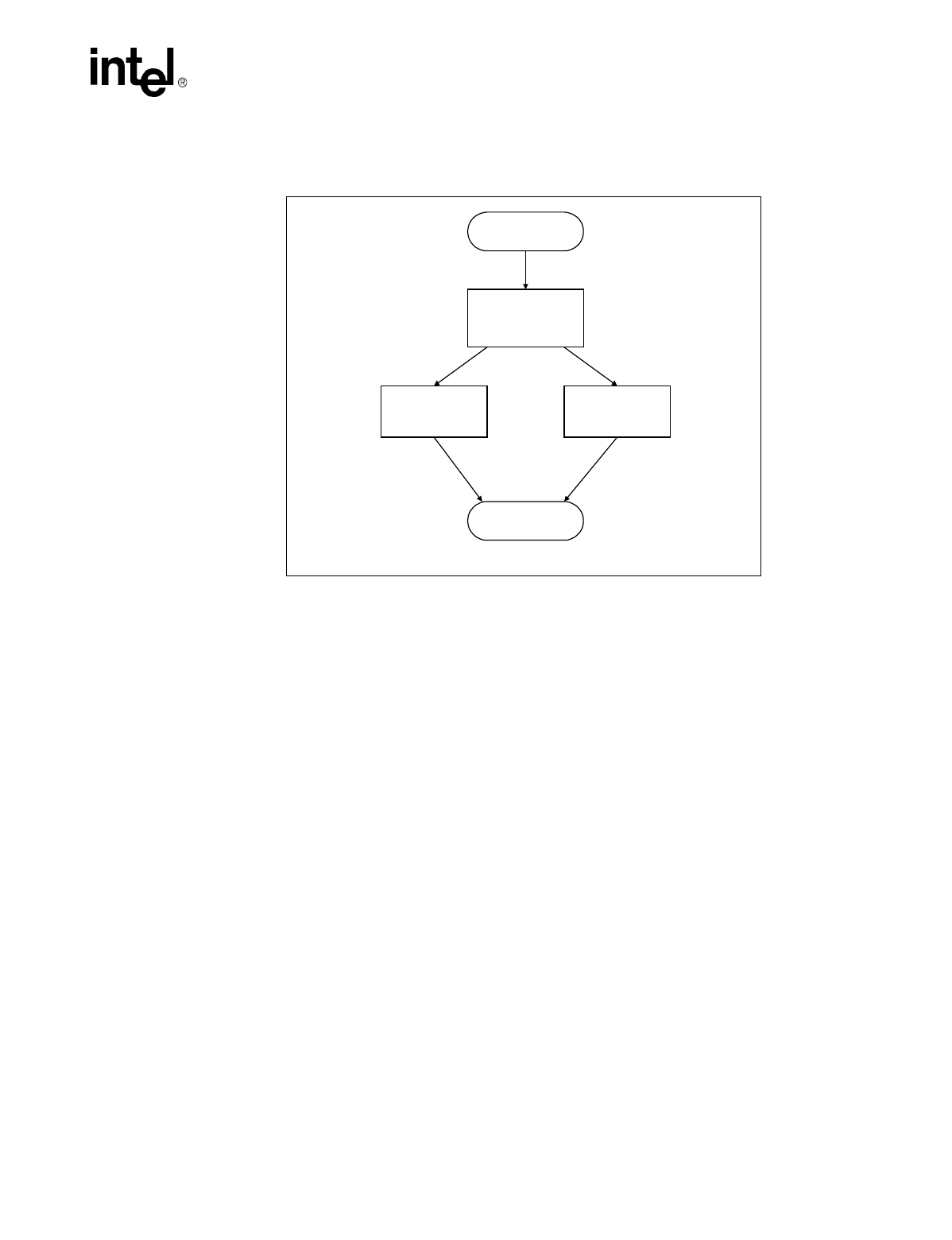
Datasheet 37
Networking Silicon — 82555
Negotiation or Parallel Detection with no data packets being transmitted. Connection is then
established either by FLP exchange or Parallel Detection. The 82555 will look for both FLPs and
link integrity pulses. The following diagram illustrates this process.
Figure 10. Auto-Negotiation and Parallel Detect
Force_Fail
Ability detect either by
parallel detect or auto-
negotiation.
10Base-T or
100Base-TX Link
Ready FLP capable
LINK PASS
Parallel Detection Auto-Negotiation
Look at Link Pulse;
Auto-Negotiation capable = 0 Auto-Negotiation capable = 1
Ability Match
Auto-Negotiation Complete bit set

82555 — Networking Silicon
38 Datasheet

Datasheet 39
Networking Silicon — 82555
9.0 LED Descriptions
The 82555 supports four LED pins to indicate link status, network activity and network speed.
•Link: This LED is off (logic high) until a valid link has been detected. After a valid link has
been detected, the LED will remain on (active-low).
•Activity: This LED is on (active-low) when activity is detected on the wire. In DTE (adapter)
mode, this LED is on during transmit and receive when the 82555 is not in loopback mode. In
repeater mode, this LED is on only during receive when the 82555 is not in loopback mode.
•Speed: This LED will be on if a 100BASE-TX link is detected and off if a 10BASE-T link is
detected. If the link fails while in Auto-Negotiation, this LED will keep the last valid link state.
If 100BASE-TX link is forced this LED will be on, regardless of the link status. This LED will
be of if the 10BASE-T link is forced, regardless of the link status.
•Full Duplex: The FDX_N signal can operate as a LED if it is enabled. It indicates full duplex
link for either 100BASE-TX or 10 BASE-T technology.
MDI register 27 in Section 7.2.3.9, “Register 27: 82555 Special Control Bit Definitions” on
page 34 details the information for LED function mapping and support enhancements.

82555 — Networking Silicon
40 Datasheet

Datasheet 41
Networking Silicon — 82555
10.0 Reset and Miscellaneous Test Modes
10.1 Reset
When the 82555 RESET signal is asserted (high), all internal circuits are reset. TXC and RXC
should run continuously even though RESET is active. The 82555 may also be reset through the
MDI reset bit.
10.2 Loopback
When the loopback pin is being driven high, the 82555 executes a loopback diagnostics operation.
This mode can also be accessed through the MDI registers.
10.3 Scrambler Bypass
When the Scrambler Bypass pin is active, the 82555 bypasses the scrambler/descrambler. This
mode can also be accessed through the MDI registers.
10.4 Test Port
When the TESTEN pin is high, the test pins provide a test access port for the 82555. In test mode,
the 82555 will default to address 1. The 82555 has a simple Test Access Port (TAP) from which all
the test modes are selected and test instructions are operated. The TAP is controlled by a simple
mechanism and handshake. Activation of all test modes requires simple hardware. The TAP signals
connected to the 82555 blocks and periphery control the 82555’s mode of operation to allow simple
testing and internal built-in self testing.
The test instruction are shifted into the Test Instruction Shift Register (TISR) through the TIN pin.
The TIN pin is sampled on the rising edge of the TCK input signal. The instruction is transferred
from the TISR to the Test Instruction Register (TIR) when TESTEN is sampled high on the rising
edge of TCK. As a general rule, all the TAP input and output pins are activated by the rising edge of
TCK. If TCK is a constant clock signal, then TESTEN must be 1 clock pulse width.
When the TIR receives a new instruction, the instruction is decoded into control signals and
synchronized to the 10 MHz clock. These control signals set the 82555 blocks into various test
modes. In order to achieve stable synchronization between the clock signal (X1) and the TCK
signal, the TCK input signal frequency should be less than or equal to half of the clock input signal
frequency.

82555 — Networking Silicon
42 Datasheet
The TOUT pin is controlled by different sources according to the active test instruction. The TOUT
signal is activated by the falling edge of TCK. The TAP must be reset during power-up. Otherwise,
the 82555 can wake-up during high-Z mode or NAND Test, which can be harmful to the board.
The TAP should be reset only with a hardware reset input pin and not with software reset. The
TOUT control logic selects the TISR output in all tests, except burn-in test modes.
Table 6. Test Instruction Coding
Number Code Test Instruction Select Input to TOUT
1 00000 Idle TISR D4out
2 00001 Reserved TISR D4out
3 00010 High-Z High-Z
4 00011 NAND Test TISR D4out

Datasheet 43
Networking Silicon — 82555
11.0 Electrical Specifications and Timing Parameters
11.1 Absolute Maximum Ratings
11.2 General Operating Conditions
11.3 DC Characteristics
11.3.1 MII DC Characteristics
11.3.2 10BASE-T Voltage/Current DC Characteristics
Symbol Parameter Description Min Typ Max Units
TCCase temperature under bias 0 85 C
TSStorage temperature -65 140 C
VSUP Supply voltage -0.5 7.0 V
VOAa
a. Stresses above the listed under absolute maximum ratings may cause permanent damage to the
device. This is a stress rating only and functional operations of the device at these or any other
conditions above those indicated in the operational sections of this specification is not implied. Ex-
posure to absolute maximum rating conditions for extended periods may affect device reliability.
All output voltages -0.5 7.0 V
VOTD Transmit Data Output Voltage -0.5 8.0 V
VIA All input voltages -1.0 6.0 V
Symbol Parameter Description Min Typ Max Units
VCC Supply voltage 4.75 5.25 V
TCCase temperature 0 85 C
Symbol Parameter Description Condition Min Typ Max Units
VIL Input low voltage (TTL) 0 0.8 V
VIH Input high voltage (TTL) 2.0 V
VOL Output low voltage Iout = 4 mA 0.45 V
VOH Output high voltage Iout = -4 mA 2.4 V
IIL Input low leakage current 0 < Vin < VCC ±15 µA
CINa
a. This parameter is only characterized, not tested. It is valid for digital pins only.
Input capacitance 10 pF
Symbol Parameter Description Condition Min Typ Max Units
RID10aInput differential resistance DC and VRDP =
(VCC/2) + 0.5 V 10 KΩ

82555 — Networking Silicon
44 Datasheet
11.3.3 100BASE-TX Voltage/Current DC Characteristics
VIDA10 Input differential accept voltage 5 MHz ≤
f
≤ 10 MHz ±585 ±3100 mVP
VIDR10 Input differential reject voltage 5 MHz ≤
f
≤ 10 MHz ±300 mVP
VICM10 Input common mode voltage VCC/2 V
VOD10 Output differential voltage RL = 100 Ωb
RBIAS10 = 768 Ω±2.2 ±2.8 V
ICCT10cLine driver supply RBIAS10 = 768 Ω110 mA
ICC10dCurrent on all VCC pins 120 mA
ICCT10TOT Total supply current 230 mA
LILA10eLeakage on analog pins 20 mA
a. This value is measured across the receive differential pins, RDP and RDN.
b. RL is the resistive load across the receive differential pins, RDP and RDN.
c. Transmitter current is measured with a 1:1 transformer on the center tap.
d. Current is measured on all VCC pins at VCC = 5.25 V.
e. The analog pins are: TDP, TDN, RDP, RDN, RBIAS10, and RBIAS100.
Symbol Parameter Description Condition Min Typ Max Units
Figure 11. RBIAS10 Resistance versus ICCT10
805
Ω
768
Ω
735
Ω
105mA 110mA 115mA
Icct10
Rbias10
Symbol Parameter Description Condition Min Typ Max Units
RID100 Input differential resistance
DC
VRDP = (VCC/2) +
0.5 V
VRDN = (VCC/2) -
0.5 V
10 KΩ
VIDA100 Input differential accept voltage ±500 mVP
VIDR100 Input differential reject voltage ±100 mVP
VICM100 Input common mode voltage VCC/2 V
VOD100aOutput differential voltage RBIAS100 = 634 Ω±0.95 ±1.00 ±1.05 VP
ICCT100bLine driver supply RBIAS100 = 634 Ω40 mA
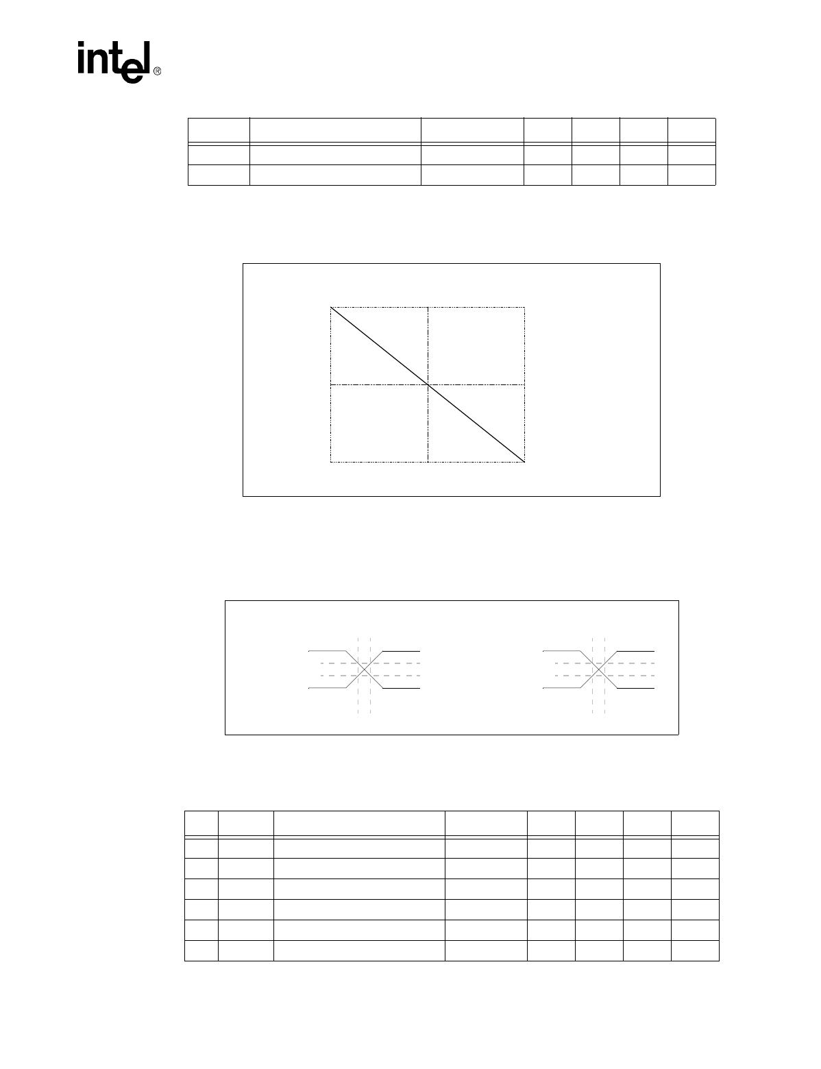
Datasheet 45
Networking Silicon — 82555
11.4 AC Characteristics
11.4.1 MII Clock Specifications
ICC100cCurrent on all VCC pins 235 mA
ICCT100TOT Total supply current 275 mA
a. Transmitter current is measured with a 1:1 transformer on the center tap.
b. Transmitter current is measured with a 1:1 transformer on the center tap.
c. Current is measured on all VCC pins at VCC = 5.25 V.
Symbol Parameter Description Condition Min Typ Max Units
Figure 12. RBIAS100 Resistance versus ICCT100
667
Ω
634
Ω
604
Ω
38mA 40mA 42mA
Icct100
Rbias100
Figure 13. AC Testing Level Conditions
Output Levels Input Levels
VIH = 2.0 V
VIL = 0.8 VVOL = 0.45 V
VOH = 2.4 V
Symbol Parameter Conditions Min Typ Max Units
T1 TP100 TXC/RXC period 100 Mbps 40 ns
T2 TP10 TXC/RXC period 10 Mbps 400 ns
T3 TPMDC MDC clock period 400 ns
T4 TTXDC TXC duty cycle 35 65 %
T5 TRXDC RXC duty cycle 35 65 %
T6 TMDC MDC duty cycle 35 65 %
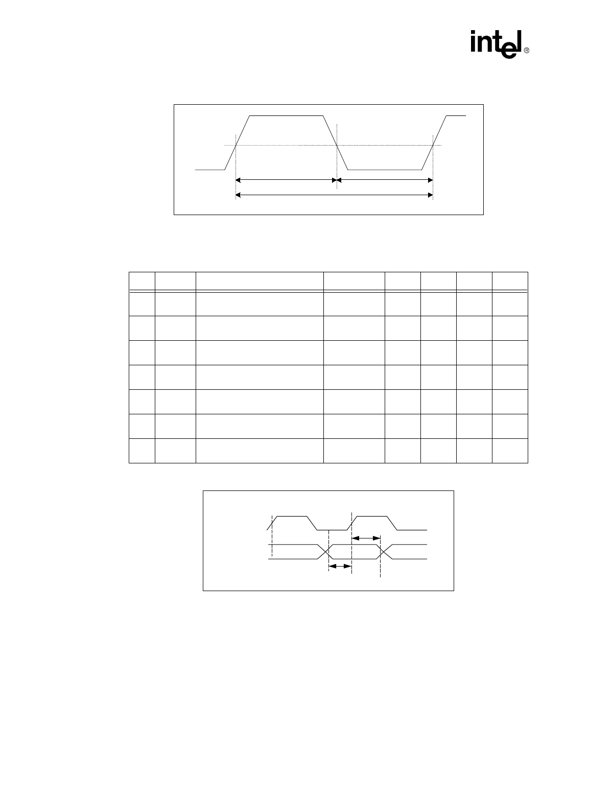
82555 — Networking Silicon
46 Datasheet
11.4.2 MII Timing Parameters
Figure 14. MII Clocks AC Timing
T1,T2,T3
1.5V
T4,T5,T6 T4,T5,T6
Symbol Parameter Conditions Min Typ Max Units
T7 TTXDV TXD[3:0], TXEN, TXERR setup
from the rising edge of TXC 15 25 ns
T8 TTXH TXD[3:0], TXEN, TXERR hold
time after the rising edge of TXC 0ns
T9 TRXSU RXD[3:0], RXDV, RXERR valid
before the rising edge of RXC 10 ns
T10 TRXH RXD[3:0], RXDV, RXERR hold
time after the rising edge of RXC 10 ns
T11 TMSU MDIO setup time to the rising
edge of MDC MDIO input 10 ns
T12 TMH MDIO hold time from the rising
edge of MDC MDIO input 10 ns
T13 TMV MDIO valid from the rising edge
of MDC MDIO output 300 ns
Figure 15. MII Transmit Timing Parameters
T7
T8
TXCLK
TXD[3:0],
TXER,TXEN Data InvalidData Invalid Data Valid
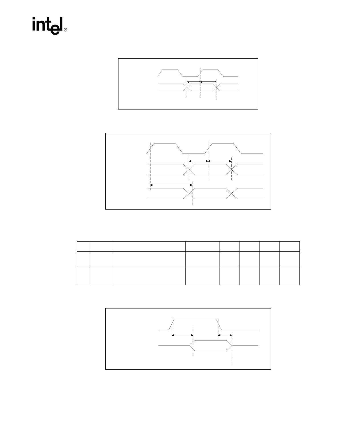
Datasheet 47
Networking Silicon — 82555
11.4.3 Repeater Mode Timing Parameters
Figure 16. MII Receive Timing Parameters
Figure 17. MII Timing Parameters: MDC/MDIO
T9 T10
RXCLK
RXD[3:0],
RXER,RXDV
Data InvalidData Invalid Data Valid
T11 T12
MDC
MDIO (Input)
Data InvalidData Invalid Data Valid
T13
MDIO (Output)
Data InvalidData Invalid Data Valid
Symbol Parameter Conditions Min Typ Max Units
T14 TRDRV PORTEN assertion to RXD[3:0],
RXDV, and RXERR (RXC driven) 1.5 2.5 RXC
clocks
T15 TRTST
PORTEN de-assertion to
RXD[3:0], RXDV, and RXERR
(RXC tri-stated)a
a. RXC, RXDV, and RXERR are tri-stated only after they have been driven low (0).
1.5 2.5 RXC
clocks
Figure 18. PORT Enable Timing
T14 T15
PORTEN
RXD[3:0],
RXER,RXDV,
RXCLK
Si
g
nal Driven
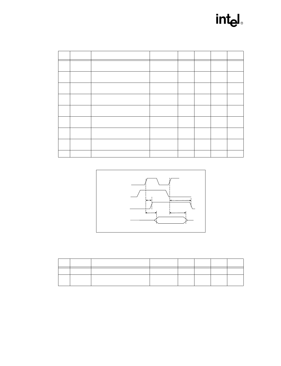
82555 — Networking Silicon
48 Datasheet
11.4.4 Transmit Packet Timing Parameters
11.4.5 Squelch Test Timing Parameters
Symbol Parameter Conditions Min Typ Max Units
T15 TXEN_ST TXC on first TXEN active to start
of frame 100 Mbps 10 12 bits
T15a TXEN_ST TXC on first TXEN active to start
of frame 10 Mbps 3.5 5 bits
T16 TXEN_CRSH TXC on first TXEN active to
rising edge of CRS 100 Mbps 4 bits
T16a TXEN_CRSH TXC on first TXEN active to
rising edge of CRS 10 Mbps 1.5 bits
T17 TXEN_END TXC on first TXEN inactive to
end of frame 100 Mbps 17 bits
T17a TXEN_END TXC on first TXEN inactive to
end of frame 10 Mbps 5 bits
T18 TXEN_CRSL TXC on first TXEN inactive to
falling edge of CRS 100 Mbps 11 bits
T18a TXEN_CRSL TXC on first TXEN inactive to
falling edge of CRS 10 Mbps 6 bits
T19 TEOF End of frame high time 10 Mbps 250 350 ns
Figure 19. Transmit Frame Timing Parameters
TXEN
CRS
Valid Frame Data
TXCLK
Frame On link
T15,T15a
T16,T16a
T17,T17a
T18,T18a
Symbol Parameter Conditions Min Typ Max Units
T20 TSQE_DEL Collision detect heartbeat delay 10 Mbps 7 8 bits
T21 TSQE_DUR Collision detect heartbeat
duration 10 Mbps 9 11 bits
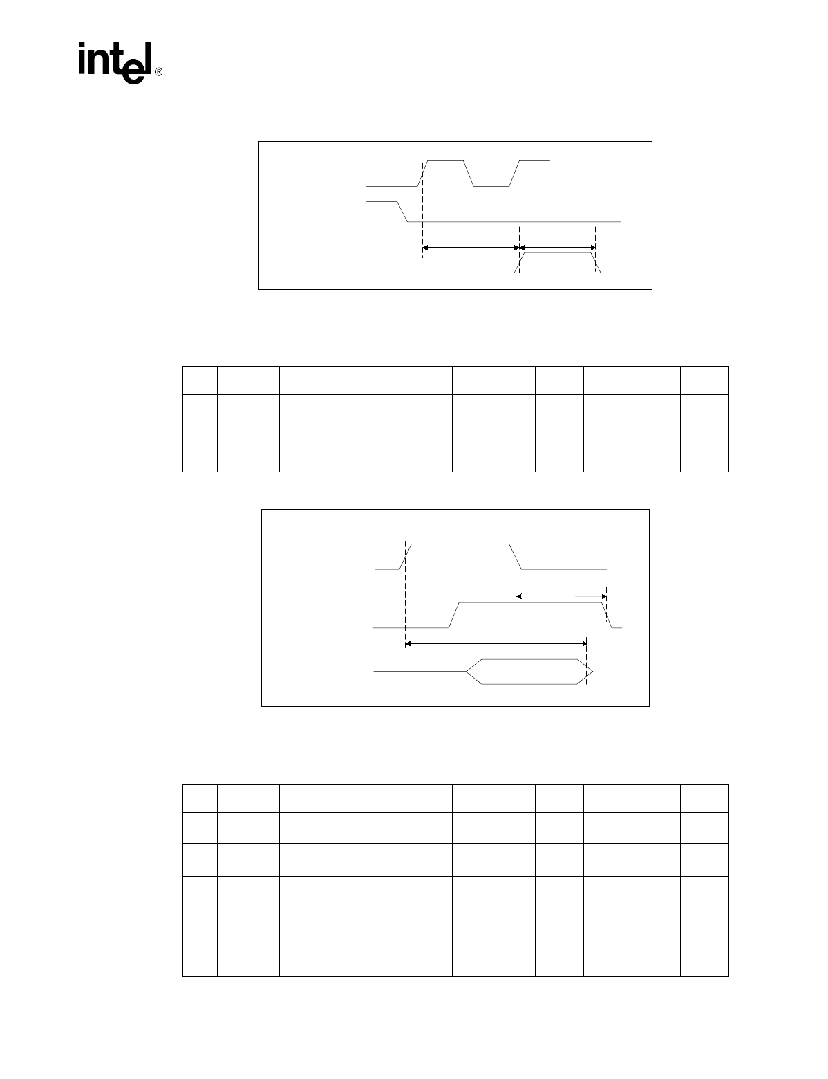
Datasheet 49
Networking Silicon — 82555
11.4.6 Jabber Timing Parameters
11.4.7 Receive Packet Timing Parameters
Figure 20. Squelch Test Timing Parameters
TXEN
COL
TXCLK
T20 T21
Symbol Parameter Conditions Min Typ Max Units
T22 TJAB_ON
Jabber turn-on delay (TXEN
asserted to end of transmit
frame) 10 Mbps 26 ms
T23 TJAB_OFF Jabber turn-off delay (TXEN de-
asserted to falling edge of COL) 10 Mbps 410 ms
Figure 21. Jabber Timing Parameters
TXEN
COL
TDP/TDN
T22
T23
Symbol Parameter Conditions Min Typ Max Units
T24 TR_CRSH Start of receive frame to rising
edge of CRS 100 Mbps 11 13 bits
T24a TR_CRSH Start of receive frame to rising
edge of CRS 10 Mbps 3 5 bits
T25 TR_RXDVH Start of receive frame to rising
edge of RXDV 100 Mbps 15 bits
T25a TR_RXDVH Start of receive frame to rising
edge of RXDV 10 Mbps 22 bits
T26 TR_CRSL End of receive frame to falling
edge of CRS 100 Mbps 14 16 bits
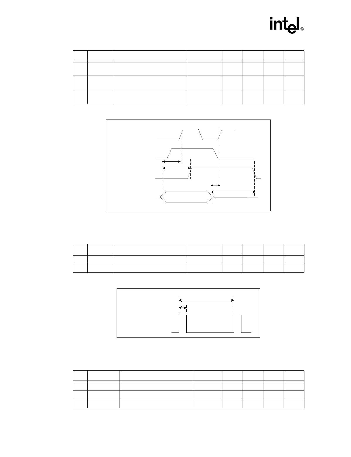
82555 — Networking Silicon
50 Datasheet
11.4.8 10BASE-T Normal Link Pulse (NLP) Timing Parameters
11.4.9 Auto-Negotiation Fast Link Pulse (FLP) Timing Parameters
T26a TR_CRSL End of receive frame to falling
edge of CRS 10 Mbps 4.5 bits
T27 TR_RXDVL End of receive frame to falling
edge of RXDV 100 Mbps 12 bits
T27a TR_RXDVL End of receive frame to falling
edge of RXDV 10 Mbps 4 bits
Symbol Parameter Conditions Min Typ Max Units
Figure 22. Receive Packet Timing Parameters
RXDV
CRS
Valid Frame Data
RXCLK
Frame On link
T25,T25a
T24,T24a
T26,T26a
T27,T27a
Symbol Parameter Conditions Min Typ Max Units
T28 TNLP_WID NLP width 10 Mbps 100 ns
T29 TNLP_PER NLP period 10 Mbps 8 24 ms
Figure 23. Normal Link Pulse Timing Parameters
Normal Link Pulse
T29
T28
Symbol Parameter Conditions Min Typ Max Units
T30 TFLP_WID FLP width (clock/data) 100 ns
T31 TFLP_CLK_CLK Clock pulse to clock pulse period 111 125 139 µs
T32 TFLP_CLK_DAT Clock pulse to data pulse period 55.5 62.5 69.5 µs
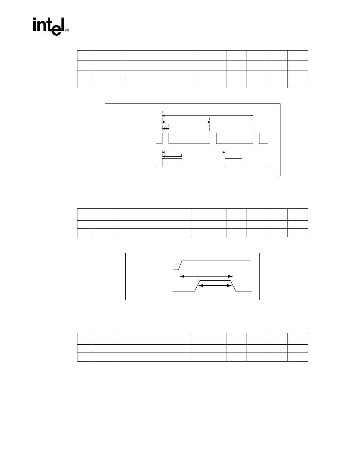
Datasheet 51
Networking Silicon — 82555
11.4.10 Reset Timing Parameters
11.4.11 X1 Clock Specifications
T33 TFLP_BUR_NUM Number of pulses in one burst 17 33
T34 TFLP_BUR_WID FLP Burst width 2 ms
T35 TFLP_BUR_PER FLP burst period 8 24 ms
Symbol Parameter Conditions Min Typ Max Units
Figure 24. Fast Link Pulse Timing Parameters
Fast Link Pulse
T31
T30
T30
Clock Pulse Data Pulse Clock Pulse
FLP Bursts
T34
T35
Symbol Parameter Conditions Min Typ Max Units
T36 TRST_WID Reset pulse width 500 ns
T37 TPUP_RST Power-up to falling edge of reset 500 µs
Figure 25. Reset Timing Parameters
Power Up
(
VCC
)
RESET
T37
T36
Symbol Parameter Conditions Min Typ Max Units
T38 TX1_DC X1 duty cycle 40 60 %
T39 TX1_PR X1 period ±50 PPM 40 ns

82555 — Networking Silicon
52 Datasheet
11.4.12 100BASE-TX Transmitter AC Specification
Figure 26. X1 Clock Specifications
T38
2.5V
T39 T39
0.4V
4.0V
Symbol Parameter Conditions Min Typ Max Units
T40 TJIT TDP/TDN differential output peak
jitter HLS data 300 700 ps
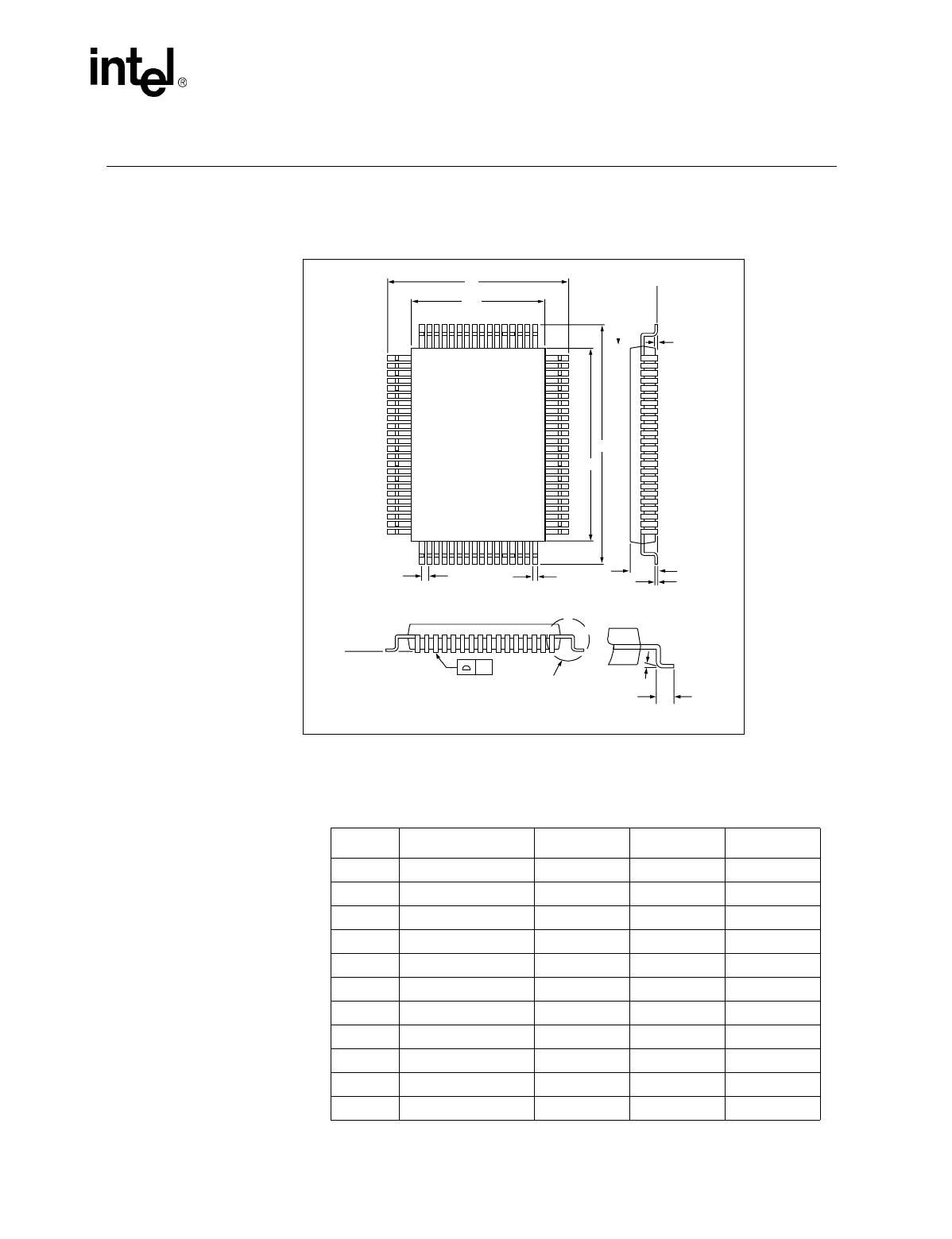
Datasheet 53
Networking Silicon — 82555
12.0 82555 Package Information
This section provides the physical packaging information for the 82555. The 82555 is an 100-pin
plastic Quad Flat Pack (QFP) device. Package attributes are provided in Table 7 and the dimensions
are shown in Figure 27.
Figure 27. Dimension Diagram for the 82555 QFP
Table 7. Dimensions for the 82555 QFP
Symbol Description Min Norm Max
N Lead Count - 100 -
A Overall Height - - 3.15
A1 Stand Off 0.05 - 0.40
b Lead Width 0.20 0.30 0.40
c Lead Thickness 0.10 0.15 0.20
D Terminal Dimension 17.5 17.9 18.3
D1 Package Body - 14.0 -
E Terminal Dimension 23.5 23.9 24.3
E1 Package Body - 20.0 -
e1 Lead Pitch 0.53 0.65 0.77
L1 Foot Length 0.60 0.80 1.00
Y
D
D1
E
E1
eb
A1
A
C
Seating
Plane
Seating
Plane
See Detail A
Detail A
TL1
PC-3712

82555 — Networking Silicon
54 Datasheet
T Lead Angle 0.0 - 10.0
Y Coplanarity - - 0.10
Table 7. Dimensions for the 82555 QFP
Symbol Description Min Norm Max
