JSW Pacific RFB01 2.4GHz WIRELESS DIGITAL TRANSCEIVER MODULE User Manual
JSW Pacific Corporation 2.4GHz WIRELESS DIGITAL TRANSCEIVER MODULE Users Manual
Users Manual

FJK_RF_7121_A
Wireless Digital Transceiver RFB01
A72121 17 dBm module specification
MD7121-F07(-05)
JSW
Data Sheet
CUSTOMER____________________
PRODUCT :2.4GHz Wireless digital
Transceiver Module
MODEL NO. RFB01
DATE: 2011-7-15

FJK_RF_7121_A
Wireless Digital Transceiver RFB01
Rev. NO. History Issue Date Remark
0.0
0.1
0.2
0.3
Table of Contents
1. General Description ………………………………………… 3
2. Electrical specfication ……………………………………… 3
3. Interface ……………………………………………………… 4
4. PA&LNA control state ………………………………………… 4
5. Application circuit …………………………………………… 5
6. Timing contril for passing CE/FCC ………………………… 6

FJK_RF_7121_A
Wireless Digital Transceiver RFB01
1. General Description
The MD7121 module is designed for 2.4GHZ ISM band with 17dBm output power wireless
applications using AMICCOM’s A7121 FSK/GFSK transceiver and A7700 RF Front End IC, This
module features a fully programmable frequency synthesizer by SPI, The data rata is 1Mbps and
3Mbps.
2. Electrical speification
Item Specification Remark
Supply voltage 3.3V+/-0.1(V)
Current consumption
15uA@Sleep mode
(Sleep current includes power consumption of LDO)
1.5mA@Stand-by mode
11Ma@Synthesizer Mode
130mA@Tx power =17dBm
36Ma@ Rx mode
typical
Frequency 2414.25~2461.5MHZ ISM band
Tranmit output power 17dBm@Maximum Power Setting*1 typical
Rx sensitivity
-93dBm(typical)@1M mode,Dev=250KHZ
-88dBm(typical)@3M mode,Dev=750KHZ
BER≤1E-3,FSK
Modulation FSK and GFSK
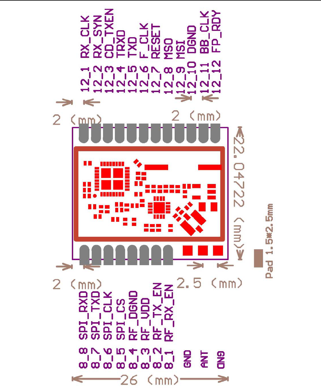
Interface 20 pin1.27mm header
PCB Dimension 29(L)*29(W)*0.8(H)mm3without antenna
Operating temperature 0~50℃
3. Interface
Pin NO. Pin name Comment Note
1 SPI_CS SPI chip select
2 SPI_CLK SPI clock
3 SPI_RXD SPI data input

FJK_RF_7121_A
Wireless Digital Transceiver RFB01
4 SPI_TXD SPI data output
5 SPI_CLK RX data sampling clock output
6 SPI_SYN RX sync signal output
7 SPI_TXEN TX mode:Modulation enable
RX mode:Carrier detector
8 TRXD Input:TX data input
Output:RX data output
9 TXD TX data input
10 F_CLK Clock for FIFO data
11 RESETN Chip reset
12 MS0 Transceiver operation mode selection input
13 MS1 Transceiver operation mode selection input
14 BB_CLK Clock output
15 VIN RF module supply voltage input
16 GND GND
17 FP_RDY Multi-function pin of FIFO packet R/W
Complete or ready sinynal
18 GND GND
19 TXSW RF front end PA/LNA select
20 RXSW RF front end PA/LNA select
4. PA&LNA control state
Control function RX ON TX ON TRX OFF Inhibit
TXSW 1 0 1 0
RXSW 0 0 1 0
5. Pin Configuration and Mechanical Information
FJK_RF_7121_A
Wireless Digital Transceiver RFB01
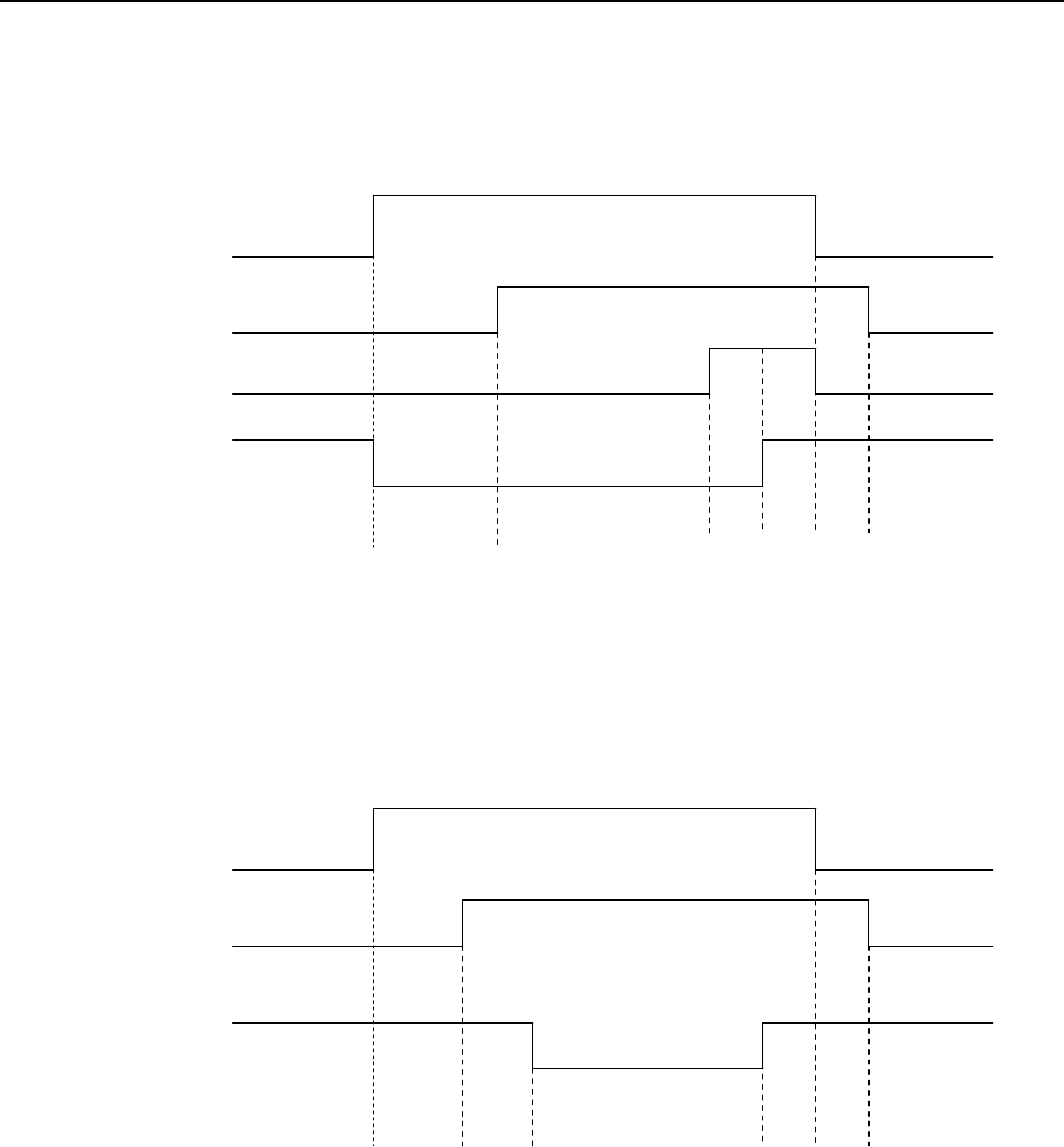
6.Timing Control for passing CE/FCC:
FJK_RF_7121_A
Wireless Digital Transceiver RFB01
(1) FOR FIFO mode operation:
If customers use FIFO Mode,the max.output power of MD7172-F07 should be set
to 15dBm in order to pass CE/FCC
A7121MSI
A7121 CD_TXEN
FP_RDY
A7700_TXSW
60uS 4us 2us 2us
(2)
FOR FIFO mode operation:
For passing CE/FCC regulation,customers can use the timing control below and set
the output power to 17dBm.
A7121MSI
A7121 CD_TXEN
A7700_TXSW
60uS 5us 2us 2us

FJK_RF_7121_A
Wireless Digital Transceiver RFB01
FCC NOTE:
This device complies with Part 15 of the FCC Rules. Operation is subject to the following two conditions: (1) this device may
not cause harmful interference, and (2) this device must accept any interference received, including interference that may cause
undesired operation.
The antenna used for this transmitter must not be co-located or operated in conjunction with any other antenna or transmitter.
All antennas in the final product must be at least 20 cm from users and nearby persons.
The manufacturer is not responsible for any radio or TV interference caused by unauthorized modifications to this equipment.
Such modifications could void the user's authority to operate the equipment.
Note: This equipment contains module, FCC ID: LE2RFB01, which qualifies as an UNLICENSED MODULAR
TRANSMITTER per FCC Public Notice DA 00-1407. It has been tested and found to comply with Part 15.247 of the FCC
Rules. This module has been designed for use by the JSW Pacific Corp.
Required labeling. Any device incorporating this module must include an external, visible, permanent marking or label which
states: ”Contains FCC ID: LE2RFB01.” Failure to comply with this requirement will void the user’s authority to operate any
device that incorporates this module.
This equipment complies with FCC radiation exposure limits set forth for uncontrolled equipment and meets the FCC radio
frequency (RF) Exposure Guidelines in Supplement C to OET65.