KAB Enterprise ECO-PLUGS Wi-Fi Module User Manual
Kab Enterprise Co., Ltd. Wi-Fi Module
user manual

KAB Enterprise Co., Ltd
Wi-Fi Smart Switch
Disclaimer and Copyright Notice
Information in this document, including URL references, is subject to change without notice.
THIS DOCUMENT IS PROVIDED AS IS WITH NO WARRANTIES WHATSOEVER, INCLUDING ANY
WARRANTY OF MERCHANTABILITY, NON-INFRINGEMENT, FITNESS FOR ANY PARTICULAR PURPOSE,
OR ANY WARRANTY OTHERWISE ARISING OUT OF ANY PROPOSAL, SPECIFICATION OR SAMPLE. All
liability, including liability for infringement of any proprietary rights, relating to use of information in this
document is disclaimed. No licenses express or implied, by estoppel or otherwise, to any intellectual property
rights are granted herein.
The WiFi Alliance Member Logo is a trademark of the WiFi Alliance.
All trade names, trademarks and registered trademarks mentioned in this document are property of
their respective owners, and are hereby acknowledged.
Copyright © 2015 KAB Enterprise Co., Ltd. All rights reserved.
1.1. Features
802.11 b/g/n
Integrated low power 32-bit MCU
Integrated 10-bit ADC
Integrated TCP/IP protocol stack
Integrated TR switch, balun, LNA, power amplifier and matching network
Integrated PLL, regulators, and power management units
Supports antenna diversity
Wi-Fi 2.4 GHz, support WPA/WPA2
Support STA/AP/STA+AP operation modes
Support Smart Link Function for both Android and iOS devices
SDIO 2.0, (H) SPI, UART, I2C, I2S, IRDA, PWM, GPIO
A-MPDU & A-MSDU aggregation and 0.4s guard interval
Deep sleep power <10uA, Power down leakage current < 5uA
Wake up and transmit packets in < 2ms
Standby power consumption of < 1.0mW (DTIM3) •
Operating temperature range -40C ~ 125C
FCC, Wi-Fi Alliance, certified

1.2. Parameters
Table 1 below describes the major parameters.
Table 1 Parameters
Categories Items Values
Certificates FCC/CE/TELEC
WiFi Parameters WiFi Protocols 802.11 b/g/n
Frequency Range 2.4GHz-2.5GHz (2400M-2483.5M)
UART/SDIO/SPI/I2C/I2S/Ir Remote Control
Peripheral Bus GPIO/PWM
Operating Voltage 3.0~3.6V
Hardware Operating Current Average value: 80mA
Parameters Operating Temperature Range -40°~125°
Ambient Temperature Range Normal temperature
Package Size 18mm*20mm*3mm
External Interface N/A
Wi-Fi mode station/softAP/SoftAP+station
Security WPA/WPA2
Encryption WEP/TKIP/AES
Software
Firmware Upgrade
UART Download / OTA (via network) /
download and write firmware via host
Parameters
Software Development
Supports Cloud Server Development / SDK for
custom firmware development
Network Protocols IPv4, TCP/UDP/HTTP/FTP
User Configuration
AT Instruction Set, Cloud Server, Android/iOS
App
2. Pin Descriptions
There are altogether 18 pin counts, the definitions of which are described in Table 2 below.
Table 2 Pin Descriptions
NO. Pin Name Function
1 3V3 3.3V power supply (VDD)
2 EN Chip enable pin. Active high.
3 IO14 GPIO14; HSPI_CLK
4 IO12 GPIO12; HSPI_MISO
5 IO13 GPIO13; HSPI_MOSI; UART0_CTS
6 IO15 GPIO15; MTDO; HSPICS; UART0_RTS
7 IO2 GPIO2; UART1_TXD
8 IO0 GPIO0
9 GND GND
10 IO4 GPIO4
11 RXD UART0_RXD; GPIO3
12 TXD UART0_TXD; GPIO1
13 GND GND
14 IO5 GPIO5
15 RST Reset the module
16 TOUT
It can be used to test the power-supply voltage of VDD3P3 (Pin3 and
Pin4) and the input power voltage of TOUT (Pin 6). However, these two
functions cannot be used simultaneously.
17 IO16 GPIO16; can be used to wake up the chipset from deep sleep mode.
18 GND GND
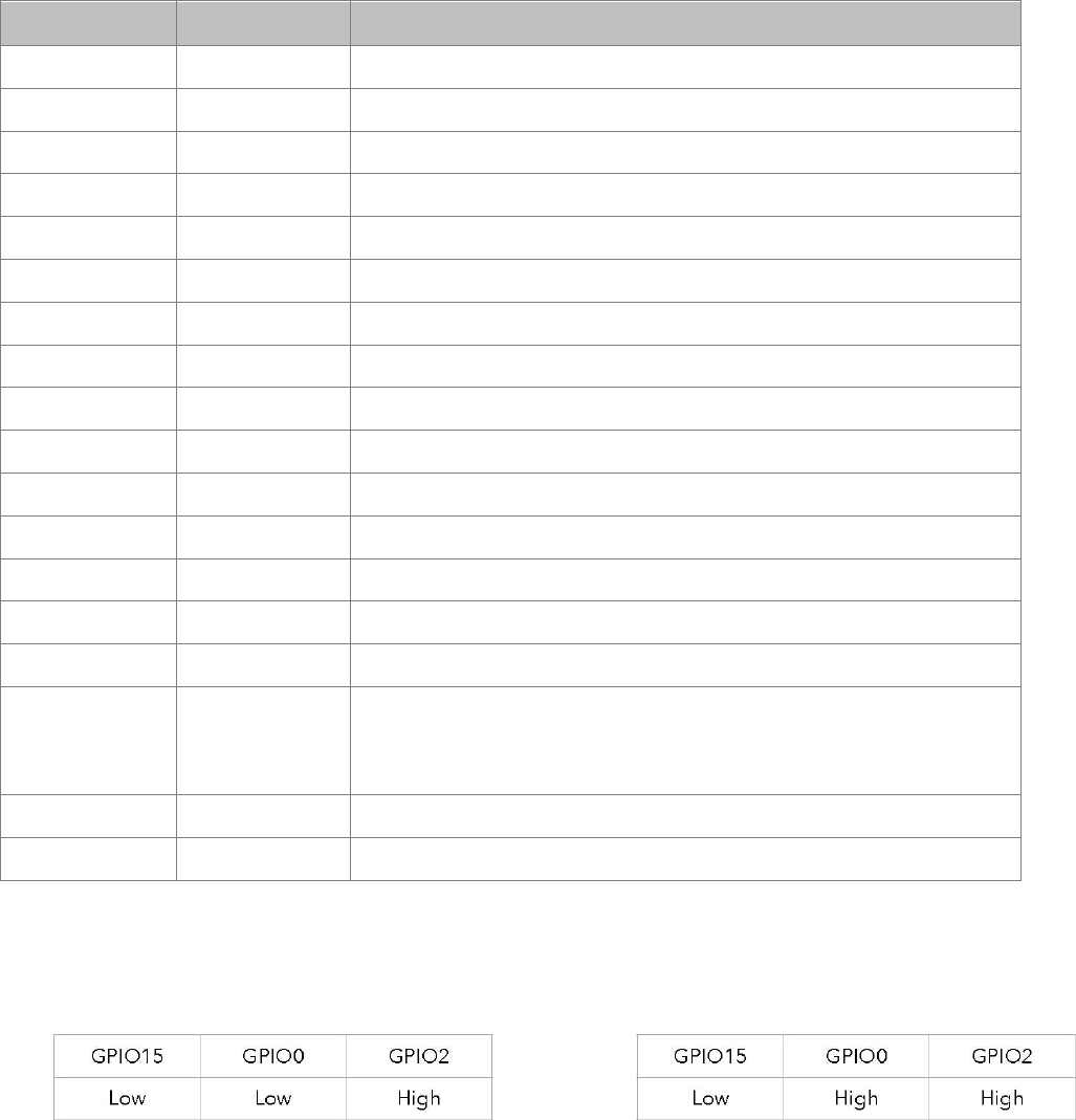
Note:
Table 3 UART Download Mode Table 4 Flash Boot Mode

The following are measured under room temperature conditions with 3.3V and 1.1V power supplies.
Table 5 Receiver Sensitivity
Parameters Min Typical Max Unit
Input frequency 2412 2484 MHz
Input impedance 50 Ω
Input reflection -10 dB
Output power of PA for 72.2Mbps 15.5 16.5 17.5 dBm
Output power of PA for 11b mode 19.5 20.5 21.5 dBm
Sensitivity
DSSS, 1Mbps -98 dBm
CCK, 11Mbps -91 dBm
6Mbps (1/2 BPSK) -93 dBm
54Mbps (3/4 64-QAM) -75 dBm
HT20, MCS7 (65Mbps, 72.2Mbps) -72 dBm
Adjacent Channel Rejection
OFDM, 6Mbps 37 dB
OFDM, 54Mbps 21 dB
HT20, MCS0 37 dB
HT20, MCS7 20 dB
3. Functional Descriptions
3.1. MCU
ESP8266EX is embedded with Tensilica L106 32-bit micro controller (MCU), which features extra low power
consumption and 16-bit RSIC. The CPU clock speed is 80MHz. It can also reach a maximum value of
160MHz.
ESP8266EX is often integrated with external sensors and other specific devices through its GPIOs; codes
for such applications are provided in examples in the SDK.
3.2. Memory Organization
1. Internal SRAM and ROM
ESP8266EX WiFi SoC is embedded with memory controller, including SRAM and ROM. MCU can visit the
memory units through iBus, dBus, and AHB interfaces. All memory units can be visited upon request, while a
memory arbiter will decide the running sequence according to the time when these requests are received by the
processor.
According to our current version of SDK provided, SRAM space that is available to users is assigned as
below:
RAM size < 36kB, that is to say, when ESP8266EX is working under the station mode and is connected
to the router, programmable space accessible to user in heap and data section is around 36kB.)
There is no programmable ROM in the SoC, therefore, user program must be stored in an external SPI
flash.
2. External SPI Flash
This module is mounted with an 2 MB external SPI fl ash to store user programs. If larger definable storage
space is required, a SPI fl ash with larger memory size is preferred. Theoretically speaking, up to 16 MB
memory capacity can be supported.
Suggested SPI Flash memory capacity:
OTA is disabled: the minimum fl ash memory that can be supported is 512 kB;
OTA is enabled: the minimum fl ash memory that can be supported is 1 MB.

Several SPI modes can be supported, including Standard SPI, Dual SPI, and Quad SPI.
Therefore, please choose the correct SPI mode when you are downloading into the fl ash, otherwise
firmwares/programs that you downloaded may not work in the right way.
3.3. Crystal
Currently, the frequency of crystal oscillators supported include 40MHz, 26MHz and 24MHz. The accuracy
of crystal oscillators applied should be ±10PPM, and the operating temperature range should be between
-20°C and 85°C.
When using the downloading tools, please remember to select the right crystal oscillator type. In circuit design,
capacitors C1 and C2, which are connected to the earth, are added to the input and output terminals of the
crystal oscillator respectively. The values of the two capacitors can be flexible, ranging from 6pF to 22pF,
however, the specific capacitive values of C1 and C2 depend on further testing and adjustment on the overall
performance of the whole circuit. Normally, the capacitive values of C1 and C2 are within 10pF if the crystal
oscillator frequency is 26MHz, while the values of C1 and C2 are 10pF<C1, C2<22pF if the crystal oscillator
frequency is 40MHz.
3.4. Interfaces
Table 7 Descriptions of Interfaces
Interface Pin Name Description
HSPI
IO12(MISO)
IO13(MOSI)
IO14(CLK)
IO15(CS)
SPI Flash 2, display screen, and MCU can be connected using HSPI interface.
PWM
IO12(R)
IO15(G)
IO13(B)
Currently the PWM interface has four channels, but users can extend the
channels according to their own needs. PWM interface can be used to control
LED lights, buzzers, relays, electronic machines, and so on.
IR Remote
Control
IO14(IR_T)
IO5(IR_R)
The functionality of Infrared remote control interface can be implemented via
software programming. NEC coding, modulation, and demodulation are used
by this interface. The frequency of modulated carrier signal is 38KHz.
ADC TOUT
ESP8266EX integrates a 10-bit analog ADC. It can be used to test the
power-supply voltage of VDD3P3 (Pin3 and Pin4) and the input power voltage
of TOUT (Pin 6). However, these two functions cannot be used
simultaneously. This interface is typically used in sensor products.
I2C IO14(SCL)
IO2(SDA)
I2C interface can be used to connect external sensor products and display
screens, etc.

Interface Pin Name Description
UART0:
TXD (U0TXD)
RXD (U0RXD)
Devices with UART interfaces can be connected with the module.
Downloading: U0TXD+U0RXD or GPIO2+U0RXD Communicating: UART0:
U0TXD, U0RXD, MTDO (U0RTS), MTCK (U0CTS) Debugging: UART1_TXD
(GPIO2) can be used to print debugging information.
UART IO15 (RTS)
IO13 (CTS)
UART1:
IO2(TXD)
By default, UART0 will output some printed information when the device is
powered on and is booting up. If this issue exerts influence on some specific
applications, users can exchange the inner pins of UART when initializing, that
is to say, exchange U0TXD, U0RXD with U0RTS, U0CTS.
I2S
I2S
I2S Input:
IO12
(I2SI_DATA) ;
IO13
(I2SI_BCK );
IO14
(I2SI_WS);
I2S Output:
IO15
(I2SO_BCK );
IO3
(I2SO_DATA);
IO2
(I2SO_WS ).
I2S interface is mainly used for collecting, processing, and transmission of
audio data.

3.5. Absolute Maximum Ratings
Table 8 Absolute Maximum Ratings
Rating Condition Value Unit
Storage Temperature -40 to 125 ℃
Maximum Soldering Temperature 260 ℃
Supply Voltage IPC/JEDEC J-STD-020 +3.0 to +3.6 V
3.6. Recommended Operating Conditions
Table 9 Recommended Operating Conditions
Operating Condition Symbol Min Typ Max Unit
Operating Temperature -40 20 125 ℃
Supply voltage VDD 3.0 3.3 3.6 V
3.7. Digital Terminal Characteristics
Table 10 Digital Terminal Characteristics
Terminals Symbol Min Typ Max Unit
Input logic level low VIL -0.3 0.25VDD V
Input logic level high VIH 0.75VDD VDD+0.3 V
Output logic level low VOL N 0.1VDD V
Output logic level high VOH 0.8VDD N V
Note: Test conditions: VDD = 3.3V, Temperature = 20 ℃, if nothing special is stated.

4. RF Performance
Description Min. Typ. Max Unit
Input frequency 2400 2483.5 MHz
Input impedance 50 ohm
Input reflection -10 dB
Output power of PA for 72.2Mbps 15.5 16.5 17.5 dBm
Output power of PA for 11b mode 19.5 20.5 21.5 dBm
Sensitivity
CCK, 1Mbps -98 dBm
CCK, 11Mbps -91 dBm
6Mbps (1/2 BPSK) -93 dBm
54Mbps (3/4 64-QAM) -75 dBm
HT20, MCS7 (65Mbps, 72.2Mbps) -72 dBm
Adjacent Channel Rejection
OFDM, 6Mbps 37 dB
OFDM, 54Mbps 21 dB
HT20, MCS0 37 dB
HT20, MCS7 20 dB
Table 10 RF Performance

5. Power Consumption
Table 11 Power Consumption
Parameters Min Typical Max Unit
Tx802.11b, CCK 11Mbps, P OUT=+17dBm 170 mA
Tx 802.11g, OFDM 54Mbps, P OUT =+15dBm 140 mA
Tx 802.11n, MCS7, P OUT =+13dBm 120 mA
Rx 802.11b, 1024 bytes packet length , -80dBm 50 mA
Rx 802.11g, 1024 bytes packet length, -70dBm 56 mA
Rx 802.11n, 1024 bytes packet length, -65dBm 56 mA
Modem-Sleep① 15 mA
Light-Sleep② 0.9 mA
Deep-Sleep③ 10 uA
①: Modem-Sleep requires the CPU to be working, as in PWM or I2S applications. According to
802.11 standards (like U-APSD), it saves power to shut down the Wi-Fi Modem circuit while maintaining a Wi-Fi
connection with no data transmission. E.g. in DTIM3, to maintain a sleep 300ms-wake 3ms cycle to receive
AP’s Beacon packages, the current is about 15mA.
②: During Light-Sleep, the CPU may be suspended in applications like Wi-Fi switch. Without data
transmission, the Wi-Fi Modem circuit can be turned off and CPU suspended to save power according to the
802.11 standard (U-APSD). E.g. in DTIM3, to maintain a sleep 300ms-wake 3ms cycle to receive AP’s
Beacon packages, the current is about 0.9mA.
③: Deep-Sleep does not require Wi-Fi connection to be maintained. For application with long time lags
between data transmission, e.g. a temperature sensor that checks the temperature every 100s, sleep 300s and
waking up to connect to the AP (taking about 0.3~1s), the overall average current is less than 1mA.

Federal Communication Commission Interference Statement
This equipment has been tested and found to comply with the limits for a Class B digital device, pursuant to Part 15
of the FCC Rules. These limits are designed to provide reasonable protection against harmful interference in a
residential installation. This equipment generates, uses and can radiate radio frequency energy and, if not installed
and used in accordance with the instructions, may cause harmful interference to radio communications. However,
there is no guarantee that interference will not occur in a particular installation. If this equipment does cause
harmful interference to radio or television reception, which can be determined by turning the equipment off and on,
the user is encouraged to try to correct the interference by one or more of the following measures:
Reorient or relocate the receiving antenna.
Increase the separation between the equipment and receiver.
Connect the equipment into an outlet on a circuit different from that to which the receiver is connected.
Consult the dealer or an experienced radio/TV technician for help.
FCC Caution: Any changes or modifications not expressly approved by the party responsible for compliance could
void the user's authority to operate this equipment.
This device complies with Part 15 of the FCC Rules. Operation is subject to the following two conditions: (1) This
device may not cause harmful interference, and (2) this device must accept any interference received, including
interference that may cause undesired operation.
FCC Radiation Exposure Statement:
This equipment complies with FCC radiation exposure limits set forth for an uncontrolled environment. This
equipment should be installed and operated with minimum distance 20cm between the radiator & your body.
LABEL OF THE END PRODUCT:
The final end product must be labeled in a visible area with the following " Contains TX FCC ID: PAGECO-PLUGS ".
This device complies with Industry Canada’s licence-exempt RSSs. Operation is subject to the following two
conditions:
(3) This device may not cause interference; and
(4) This device must accept any interference, including interference that may cause undesired operation of the
device.
Le présent appareil est conforme aux CNR d'Industrie Canada applicables aux appareils radio exempts de licence.
L'exploitation est autorisée aux deux conditions suivantes : (1) l'appareil ne doit pas produire de brouillage, et (2)
l'utilisateur de l'appareil doit accepter tout brouillage radioélectrique subi, même si le brouillage est susceptible d'en
compromettre le fonctionnement.
This radio transmitter IC: 4494A-ECOPLUGS has been approved by Industry Canada to operate with the antenna
types listed below with the maximum permissible gain indicated. Antenna types not included in this list, having a gain
greater than the maximum gain indicated for that type, are strictly prohibited for use with this device.
Antenna General Information
Ant. Cat. Ant. Type Gain
(
dBi
)
External Dipole 2.33
External Printed -4.88
Le présent émetteur radio IC: 4494A-ECOPLUGS a été approuvé par Industrie Canada pour fonctionner avec les types
d'antenne énumérés ci-dessous et ayant un gain admissible maximal et l'impédance requise pour chaque type d'antenne. Les
types d'antenne non inclus dans cette liste, ou dont le gain est supérieur au gain maximal indiqué, sont strictement interdits
pour l'exploitation de l'émetteur.
Antenna General Information
Ant. Cat. Ant. Type Gain
(
dBi
)
External Dipole 2.33
External Printed -4.88
IC Radiation Exposure Statement:
This equipment complies with IC RSS-102 radiation exposure limits set forth for an uncontrolled environment. This
equipment should be installed and operated with minimum distance 20cm between the radiator & your body.
End Product Labeling
This transmitter module is authorized only for use in device where the antenna may be installed such that 20 cm
may be maintained between the antenna and users. The final end product must be labeled in a visible area with
the following: “Contains transmitter module IC: 4494A-ECOPLUGS”.
Contient le module d'émission IC: 4494A-ECOPLUGS