Kenwood Marine Radio 762G Users Manual 1~10
762G to the manual fd7554df-1f3f-4ce4-8053-ca6929260eed
2015-01-23
: Kenwood Kenwood-Kenwood-Marine-Radio-762G-Users-Manual-263875 kenwood-kenwood-marine-radio-762g-users-manual-263875 kenwood pdf
Open the PDF directly: View PDF ![]() .
.
Page Count: 68
- CONTENTS
- GENERAL
- SYSTEM SET-UP
- OPERATING FEATURES
- REALIGNMENT
- INSTALLATION
- CIRCUIT DESCRIPTION
- SEMICONDUCTOR DATA
- DESCRIPTION OF COMPONENTS
- PARTS LIST
- EXPLODED VIEW (TK-760G)
- EXPLODED VIEW (TK-762G)
- PACKING
- ADJUSTMENT
- PC BOARD VIEWS
- DISPLAY UNIT (X54-3270-10) : TK-760G
- DISPLAY UNIT (X54-3280-10) : TK-762G
- PLL/VCO (X58-4670-XX)
- TX-RX UNIT (X57-5950-XX) (A/2) Component side view
- TX-RX UNIT (X57-5950-XX) (A/2) Foil side view
- TX-RX UNIT (X57-5950-XX) (A/2) Component side view + Foil side
- TX-RX UNIT (X57-5950-XX) (B/2) Component side view
- TX-RX UNIT (X57-5950-XX) (B/2) Foil side view
- TX-RX UNIT (X57-5950-XX) (B/2) Component side view + Foil side
- SCHEMATIC DIAGRAM (TK-760G)
- SCHEMATIC DIAGRAM (TK-762G)
- BLOCK DIAGRAM
- LEVEL DIAGRAM
- TERMINAL FUNCTION
- SPECIFICATIONS

Document Copyrights
Copyright 2006 by Kenwood Corporation. All rights reserved.
No part of this manual may be reproduced, translated, distributed, or transmitted in any
form or by any means, electronic, mechanical, photocopying, recording, or otherwise, for
any purpose without the prior written permission of Kenwood.
Disclaimer
While every precaution has been taken in the preparation of this manual, Kenwood
assumes no responsibility for errors or omissions. Neither is any liability assumed for
damages resulting from the use of the information contained herein. Kenwood reserves
the right to make changes to any products herein at any time for improvement purposes.
© 2000-1 PRINTED IN JAPAN
B51-8497-10 (N) 1269
VHF FM TRANSCEIVER
TK-760G/762G
SERVICE MANUAL
REVISED
Please use this manual in place of the service manual (preliminary version), B51-8497-00.
We have added the information on the circuit description, specifications, and K2 version specifications to the service
manual (preliminary version), B51-8497-00.
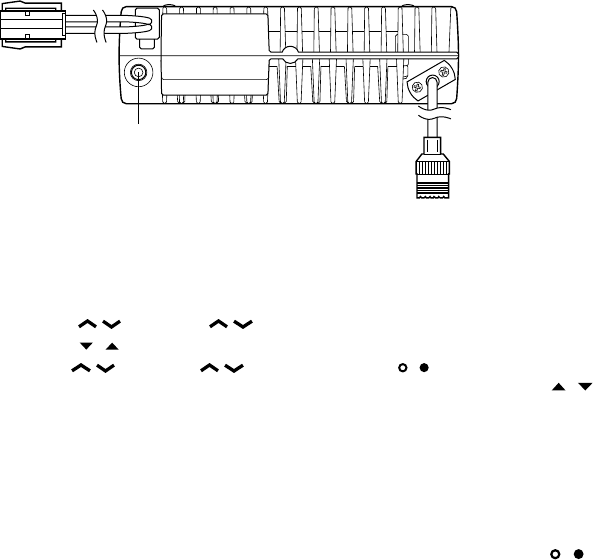
Microphone
(T91-0597-15)
Cabinet (Upper)
(A01-2165-13)
Panel assy
(A62-0642-03)
Key top
(K29-5343-02)
Microphone
(T91-0597-15)
Cabinet (Upper)
(A01-2165-13)
Panel assy
(A62-0731-03)
Key top
(K29-5344-02)
TK-760G (K)
TK-762G (K)
2
TK-760G/762G
CONTENTS / GENERAL
GENERAL
INTRODUCTION
SCOPE OF THIS MANUAL
This manual is intended for use by experienced techni-
cians familiar with similar types of commercial grade com-
munications equipment. It contains all required service in-
formation for the equipment and is current as of the publica-
tion date. Changes which may occur after publication are
covered by either Service Bulletins or Manual Revisions.
These are issued as required.
ORDERING REPLACEMENT PARTS
When ordering replacement parts or equipment informa-
tion, the full part identification number should be included.
This applies to all parts : components, kits, or chassis. If the
part number is not known, include the chassis or kit number
of which it is a part, and a sufficient description of the re-
quired component for proper identification.
PERSONNEL SAFETY
The following precautions are recommended for person-
nel safety :
• DO NOT transmit if someone is within two feet (0.6
meter) of the antenna.
• DO NOT transmit until all RF connectors are verified se-
cure and any open connectors are properly terminated.
• SHUT OFF and DO NOT operate this equipment near
electrical blasting caps or in an explosive atmosphere.
• All equipment should be properly grounded before
power-up for safe operation.
• This equipment should be serviced by a qualified techni-
cian only.
PRE-INSTALLATION CONSIDERNATIONS
1. UNPACKING
Unpack the radio from its shipping container and check
for accessory items. If any item is missing, please contact
KENWOOD immediately.
2. LICENSING REQUIREMENTS
Federal regulations require a station license for each ra-
dio installation (mobile or base) be obtained by the equip-
ment owner. The licensee is responsible for ensuring trans-
mitter power, frequency, and deviation are within the limits
permitted by the station license.
Transmitter adjustments may be performed only by a li-
censed technician holding an FCC first, second or general
class commercial radiotelephone operator’s license. There
is no license required to install or operate the radio.
CONTENTS
GENERAL ................................................................. 2
SYSTEM SET-UP ..................................................... 4
OPERATING FEATURES ......................................... 5
REALIGNMENT...................................................... 10
INSTALLATION...................................................... 20
CIRCUIT DESCRIPTION......................................... 24
SEMICONDUCTOR DATA..................................... 29
DESCRIPTION OF COMPONENTS ....................... 31
PARTS LIST ............................................................ 33
EXPLODED VIEW .................................................. 42
PACKING ................................................................ 44
ADJUSTMENT ....................................................... 45
PC BOARD VIEWS
DISPLAY UNIT (X54-3270-10) : TK-760G ........ 54
DISPLAY UNIT (X54-3280-10) : TK-762G ........ 55
PLL/VCO (X58-4670-XX) .................................. 56
TX-RX UNIT (X57-5950-XX) (A/2) ................... 57
TX-RX UNIT (X57-5950-XX) (B/2).................... 63
SCHEMATIC DIAGRAM ........................................ 67
BLOCK DIAGRAM.................................................. 75
LEVEL DIAGRAM ................................................... 78
TERMINAL FUNCTION ......................................... 80
SPECIFICATIONS................................................... 81
3
TK-760G/762G
1
3+
–
7
6
13
15
5. INSTALLATION PLANNING – CONTROL STATIONS
5-1. Antenna system
Control station. The antenna system selection depends
on many factors and is beyond the scope of this manual.
Your KENWOOD dealer can help you select an antenna sys-
tem that will best serve your particular needs.
5-2. Radio location
Select a convenient location for your control station radio
which is as close as practical to the antenna cable entry
point. Secondly, use your system’s power supply (which
supplies the voltage and current required for your system).
Make sure sufficient air can flow around the radio and power
supply to allow adequate cooling.
SERVICE
This radio is designed for easy servicing. Refer to the
schematic diagrams, printed circuit board views, and align-
ment procedures contained in this manual.
Note
When you modify your radio as described in system set-
up, take the following precaution.
The rating of pin 7 (SB) of the accessory connector cable
(KCT-19) on the rear of the radio is 13.6V (1A). Insert a 1A
fuse if you use the SB pin for external equipment.
Accessory connector
cable (KCT-19)
If you do not intend to use the 3.5-mm jack for the exter-
nal speaker, fit the supplied speaker-jack cap (B09-0235-05)
to stop dust and sand getting in.
Speaker-jack cap
(B09-0235-05)
3. PRE-INSTALLATION CHECKOUT
3-1. Introduction
Each radio is adjusted and tested before shipment. How-
ever, it is recommended that receiver and transmitter opera-
tion be checked for proper operation before installation.
3-2. Testing
The radio should be tested complete with all cabling and
accessories as they will be connected in the final installa-
tion. Transmitter frequency, deviation, and power output
should be checked, as should receiver sensitivity, squelch
operation, and audio output. Signalling equipment operation
should be verified.
4. PLANNING THE INSTALLATION
4-1. General
Inspect the vehicle and determine how and where the
radio antenna and accessories will be mounted.
Plan cable runs for protection against pinching or crush-
ing wiring, and radio installation to prevent overheating.
4-2. Antenna
The favored location for an antenna is in the center of a
large, flat conductive area, usually at the roof center. The
trunk lid is preferred, bond the trunk lid and vehicle chassis
using ground straps to ensure the lid is at chassis ground.
4-3. Radio
The universal mount bracket allows the radio to be
mounted in a variety of ways. Be sure the mounting surface
is adequate to support the radio’s weight. Allow sufficient
space around the radio for air cooling. Position the radio
close enough to the vehicle operator to permit easy access
to the controls when driving.
4-4. DC Power and wiring
1. This radio may be installed in negative ground electrical
systems only. Reverse polarity will cause the cable fuse
to blow. Check the vehicle ground polarity before installa-
tion to prevent wasted time and effort.
2. Connect the positive power lead directly to the vehicle
battery positive terminal. Connecting the Positive lead to
any other positive voltage source in the vehicle is not rec-
ommended.
3. Connect the ground lead directly to the battery negative
terminal.
4. The cable provided with the radio is sufficient to handle
the maximum radio current demand. If the cable must be
extended, be sure the additional wire is sufficient for the
current to be carried and length of the added lead.
GENERAL
4
TK-760G/762G
SYSTEM SET-UP
Merchandise received
License and frequency allocated by FCC
Choose the type of transceiver
Are you using the public address?
Are you using the external speaker?
Are you using ignition sense cable?
Delivery
Are you using the KGP-1A Modem GPS receiver
or the KGP-1B Modem GPS controller?
Transceiver programming (Option)
8ch models
TK-762G
128ch models
TK-760G
Frequency range (MHz)
148~174
136~162
146~174
RF power
25W
25W
25W
Type
K
K2
M
KAP-1
PA/HA unit
KCT-20
Connection cable
KES-3
External speaker
KCT-19
Accessory connector cable
KCT-18
Ignition sense cable
Frequency range (MHz)
148~174
136~162
RF power
25W
25W
Type
K
K2
See page 11.
A personal computer (IBM PC or compatible), programming interface (KPG-22),
and programming software (KPG-56D) are required for programming.
(The frequency and signalling (option) data are programmed for the transceiver.)
(Option)
(Option)
(Option)
(Option) (Option)
See page 22.
Installation the TX-RX unit when used KAP-1.
YES
YES
YES
YES
NO
NO
NO
NO
See page 21.
See page 20.
See page 23.
See the KCT-20 instruction manual
(B62-0733-11).
* : You can install either KCT-19 or KCT-20 to the
TK-760G/762G transceiver
*
*
5
TK-760G/762G
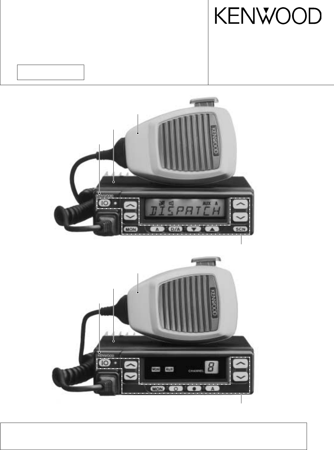
1. Controls and Functions
1-1. TK-760G Front Panel
IO (Power) switch
Press to switch the transceiver ON (or OFF).
LED indicator
Lights red while transmitting. Lights green while receiv-
ing. Flashes orange while receiving a Code Squelch or
Selective Call code, or a 2-Tone code that matches the
one set up in your transceiver.
/keys
These are PF (Programmable Function) keys. Press each
key to activate its auxiliary function. The default settings
are Volume Up and Volume Down.
Display
See right.
/keys
These are PF (Programmable Function) keys. Press each
key to activate its auxiliary function. The default settings
are Channel Up and Channel Down.
Microphone jack
Insert the microphone plug into this connector.
MON, A, D/A, , , and SCN keys (TK-760G)
MON, , , and A keys (TK-762G)
These are PF (Programmable Function) keys. Press each
key to activate its auxiliary function.
PTT (Push-to-Talk) switch
Press this switch, then speak into the microphone to call
a station.
1 2 3 4 5
76
8
1 2 3 4 5
76
1-2. TK-762G Front Panel
1-3. Microphone
1
2
3
4
5
6
7
8
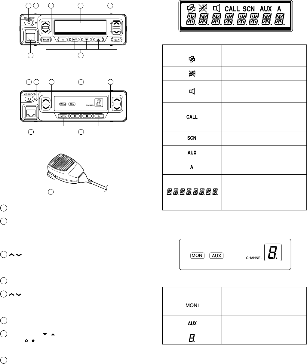
1-4. Display
■TK-760G
Indicator Description
Appears while using SmarTrunk.
Appears when the selected channel
in busy.
Appears when QT, DQT, DTMF, or
2-Tone decoding is deactivated (by
pressing the Monitor key).
Appears when you receive a Code
Squelch, Selective Call, 2-Tone code.
Also appears when you transmit
using Code Squelch or Selective Call.
Appears while scanning.
Appears when the AUX port is
activated.
Appears when the selected channel
is included in the scanning sequence.
Displays the selected channel
number (or name), DTMF digits
(when entering digits, confirming
digits, or making a call), and mes-
sages received via Selective Call.
■TK-762G
Indicator Description
Appears when QT, DQT, DTMF, or
2-Tone decoding is deactivated (by
pressing the Monitor key).
Appears when the AUX port is
activated.
Displays the selected channel
number.
OPERATING FEATURES
6
TK-760G/762G
1-5. Rear panel
Antenna
connector
External
speaker jack
Power input
connector
1-6. Programmable Auxiliary Functions
The following keys can be programmed with the func-
tions listed below.
TK-760G : / (left side), / (right side), MON, A, D/A,
, , and SCN.
TK-762G : / (left side), / (right side), MON, , , and
A.
• AUX
• Channel Down
• Channel Up
• Display Character (TK-760G only)
• Emergency *1
• Group Down (TK-760G only)
• Group Up (TK-760G only)
• Home Channel
• Horn Alert
• Key Lock
• Monitor A (Monitor Unmute-Momentary)
• Monitor B (Monitor Unmute-Toggle)
• Monitor C (Carrier Squelch-Momentary)
• Monitor D (Carrier Squelch-Toggle)
• None (No function)
• Operator Selectable Tone *2 (TK-760G only)
• Public Address
• Redial
• Scan (TK-760G only)
• Scan Del/Add (TK-760G only)
• Selectable QT *3 (TK-760G only)
• Talk-Around
• Volume Up
• Volume Down
• 2-Tone Encode Select *4
*1 : This function can be used only with a foot switch.
*2 : This function is available for K market models only.
*3 : This function is available for M market models only.
*4 : The code for the TK-762G transceiver is not selectable.
You can transmit only one 2-Tone code, which is pre-
programmed in the transceiver.
2.Operation Features
The TK-760G/762G is a VHF FM radio designed to oper-
ate in conventional format. The programmable features are
summarized.
3.Transceiver Controls and Indicators
3-1. Front Panel Controls
All the keys on the front panel are momentary-type push
buttons. The functions of these keys are explained below.
•POWER key
Transceiver POWER key. When the power is switched
off, all the parameters are stored in memory. When the
power is switched on again, the transceiver returns to the
previous conditions.
•CHANNEL UP/DOWN key (Programmable)
•/ key (Programmable) : TK-760G only
•SCAN key (Programmable) : TK-760G only
•MONITOR key (Programmable)
•A, D/A key (Programmable) : TK-760G only
• , , A key (Programmable) : TK-762G only
•VOLUME UP/DOWN key (Programmable)
•BUSY/TX LED
The BUSY indicator (Green LED) shows that the channel
is in use. The TX indicator (Red LED) shows that you are
transmitting.
3-2. Programmable Keys
The FPU (KPG-56D) enables programmable keys to se-
lect the following functions.
AUX, Channel down, Channel up, Display character *1,
Emergency (Only foot key ; M type only), Group down *1,
Group up *1, Home channel, Horn alert, Key lock, Monitor A,
Monitor B, Monitor C, Monitor D, Operator selectable tone
(K type only), Public address, Redial, Scan *1, Scan del/add
*1, Talk around, Volume down, Volume up and None.
These functions the FPU programs to the functionkeys
and described in the following sections.
*1 : TK-760G only.
•AUX
If this key is pressed, "AUX" icon lights on the display and
AUX port which is inside of the transceiver turns to the high
level. If pressed again, the "AUX" icon goes off and the AUX
ports turns to the lower level.
•Channel up/down
When the key is pressed each time, the channel number
to be selected is incremented/decremented and repeats if
held for one second or longer.
OPERATING FEATURES
7
TK-760G/762G
•Display character (TK-760G only)
This key switches the LCD display between the group
and channel number and the group and channel name.
•Emergency (M market models only)
Pressing this key for longer than 1 second causes the
transceiver to enter the emergency mode. The transceiver
jumps to the programmed "Emergency the group and chan-
nel" and transmits for 25 seconds.
The transceiver disables mic mute while transmitting.
After finishing transmission, the transceiver receivers for 5
seconds. The transceiver mutes the speaker while receiv-
ing. Following the above sequence, the transceiver contin-
ues to transmit and receive.
•Group up/down (TK-760G only)
When the key is pressed each time, the group number to
be selected is incremented/decremented and repeats if held
for one second or longer.
•Home channel
Press this key once, the channel switches to the pre-pro-
grammed home channel.
•Horn alert
If you are called from the base station using 2-tone/DTMF
while you are away from your transceiver, you will be
alerted by the vehicle horn or some other type of external
alert. To turn the horn alert function on , press this key. A
confirmation tone sounds, (and the display shows "HA" on
the LCD *1).
If this key is pressed again, the horn alert function is
turned off.
*1 : TK-760G only.
•Key lock
Pressing this key causes the transceiver to accept entry
of only the [Vol Up/Down], [Key lock], [PTT], [Monitor A],
[Monitor B], [Monitor C], [Monitor D], and [Emergency] keys.
•Monitor
Used to release signalling or squelch when operating as a
conventional. It is also used to reset option signalling.
•Operator selectable tone (K market models only)
This key switches the pre-set decode QT/DQT and en-
code QT/DQT to OST (Operator Selectable Tone) tone pair.
Press this key, the transceiver enters to OST select
mode. In this mode, the display shows "OFF" and the opera-
tor can select one of the OST tone pair using the channel up/
down key. The display shows "TONE**" and tone pair No.
** is selected.
Press OST key again, the transceiver exits from the OST
select mode.
16 kinds of tone pair for OST can be programmed by
KPG-56D. OST is useful to access the repeater with same
radio frequency and different tone (QT/DQT).
OPERATING FEATURES
•Public address
Public address amplifies the microphone audio, and out-
puts it through a PA speaker. PA is activated by pressing
this key. A confirmation tone sounds, (and the display
shows "PA" *1). PA can be activated at anytime (scanning or
non-scanning).
The RADIO continues to scan & receive calls while in PA
mode. Pressing PTT activates PA, and will override an in-
coming call at anytime; however, no RADIO transmission
takes place.
If this key is pressed again, a confirmation tone will
sound, (the display will return to the normal channel or
SCAN display *1), and the PA function will turn off.
*1 : TK-760G only.
•Redial
If you press this key when the group/channel is dis-
played, the last transmitted DTMF code will appear on the
display. Pressing the PTT switch at this time will transmit
the displayed DTMF code.
•Scan (TK-760G only)
Press this key starts scanning. Pressing this key stops
scanning.
•Scan del/add (TK-760G only)
This key switches the currently displayed channel be-
tween "Delete" and "Add".
The "Add" channel contained in the scan sequence, and
"Delete" channel is not contained. In the scan mode, this
key switches the channnel delete or add temporarily.
•Talk around
Press this key, the transceiver uses the receive fre-
quency and the tone for transmission.
The operator can call the other party directory (without
repeater). Press this key again, the talk around function
goes off.
•Volume up/down
When the key is pressed, the volume level is increased/
decreased and repeats if held for 200ms or longer.
•None
Sounds error operation beep, and no action will occur.
Use this function when the transceiver is required to be
more simple operated.
4. Scan Operating (TK-760G only)
■Scan types
•Single group scan
You can scan all valid (ADD) channels in the displayed
group that can be selected with the group up/down key.
•Multiple group scan
You can scan all valid (ADD) channels in the all valid
(ADD) group.
8
TK-760G/762G
■SCAN start condition
One or more non-priority channels must be added to all
channels that can be scanned. The transceiver must be in
normal receive mode (PTT off).
When you activate the key programmed to the scan func-
tion, the scan starts. The scan icon "SCN" lights and "SCAN"
is indicated on alphanumeric display.
■Scan stop condition
The scan stops temporarily if the following conditions are
satisfied.
1) A carrier is detected, then signalling matches on chan-
nels for which receive the signalling is set by the pro-
gramming software.
2) A carrier is detected on the channels for which receiving
signalling is not set by the programming software or
when the monitor (signalling cancel) function is activated.
■Scan channel types
1) Priority channel is the most important channel for the
scan, and always detects a signal during scan and when
the scan stops temporarily.
2) Non-priority channels detects a signal during scan. For
the channels that can be selected with the group or chan-
nel up/down key when the scan does not occur, adds an
indicator "A" lights.
■Priority channel setting
A priority channel can be set as follows with the program-
ming software (KPG-56D).
1) Specify a priority channel as a fixed priority channel.
2) Make a selected channel, a priority channel.
■Scan type according to the priority channel
1) When no priority channel is set : Only the non-priority
channels are scanned.
If a non-priority channel stops temporarily, it stops until
there is no signal on the channel.
2) When priority channel is set : Either priority channel is
scanned.
If a non-priority channel stops temporarily, a priority chan-
nel signal is detected at certain intervals.
If a priority channel stops temporarily, it stops until there
is no signal on the priority channel.
■Revert channel
The revert channel is used to transmit during scanning
and set by the programming software (KPG-56D).
1) Priority
The transceiver reverts to the priority channel.
2) Priority with talkback
The transceiver reverts to the priority channel.
If you press PTT during a resume timer (dropout delay
time, TX dwell time) or calling, you can transmit on cur-
rent channel to answer to the call however revert channel
is set to priority channel.
After resume time, scan re-starts and transmission chan-
nel is return to priority channel.
3) Selected channel
The transceiver reverts to the channel before scanning or
the channel that you changed during scan.
4) Last called channel
The transceiver reverts to the last called channel during
the scan.
5) Last used channel
The transceiver reverts to the last used (transmitted)
channel during scan. "Last used" revert channel includes
talkback function.
6) Selected with talkback
The transceiver reverts to the channel before scanning or
the channel that you changed during scan.
■Scan end
When you reactivate the key programmed to the scan
function during scan mode, the scan ends.
The scan icon "SCN" and "SCAN" display goes off.
■Temporarily delete/add
It is possible to delete or add channel temporarily during
scan. When scan stops on unnecessary channel for ex-
ample by interference of the other party, activate the delete/
add function (for example press the key), then that channel
is deleted temporarily and scan re-start immediately.
When you would like to add the deleted channel tempo-
rarily to scan sequence, select the desired (deleted) channel
during scan, activate the delete/add function (for example
press the key) before scan re-start.
That channel is added temporarily to scan sequence. The
temporary deleted or added channels are returns to pre-set
delete/add, when the transceiver exits from scan mode.
5. Details of Features
■Time-out timer
The time-out timer can be programmed in 15 seconds
increments from 15 seconds to ten minutes. If the transmit-
ter is keyed continuously for longer than the programmed
time, the transmitter is disabled and a warning tone sounds
while the PTT button is held down. The alert tone stops
when the PTT button is released.
■PTT ID
PTT ID provides a DTMF ANI to be sent with every time
PTT (beginning of transmission, end of transmission, or
both).
You can program PTT ID "on" or "off" for each group. The
contents of ID are programmed for each channel.
The timing that the transceiver sends ID is program-
mable.
BOT : DTMF ID (BOT)/MSK ID is sent on beginning of
transmission.
EOT : DTMF ID (EOT)/MSK ID is sent on end of transmis-
sion.
Both : DTMF ID (BOT)/MSK ID is sent on beginning of
transmission and DTMF ID (EOT)/MSK ID is sent on end
of transmission.
OPERATING FEATURES

9
TK-760G/762G
■Off hook decode
If the Off hook decode function has been enabled, re-
moving and replacing the microphone on the hook has no
effect for decoding QT/DQT and option signalling.
■"TOT" pre-alert
The transceiver has "TOT pre-alert timer. This parameter
selects the time at which the transceiver generates "TOT"
pre-alert tone before "TOT" is expired.
"TOT" will be expired when the selected time passes
from a TOT pre-alert tone.
■"TOT" re-key time
The transceiver has "TOT" re-key timer. This timer is the
time you can not transmit after "TOT" exceeded. After "TOT"
re-key time expired you can transmit again.
■"TOT" reset time
The transceiver has "TOT" reset timer. This timer is the
minimum wait time allowed during a transmission that will
reset the "TOT" count.
"TOT" reset time causes the "TOT" to continue even after
PTT is released unless the "TOT" reset timer has expired.
■OST (Operator Selectable Tone)
(TK-760G K market models only)
The transceiver is capable to have "OST" function and 16
tone pair (QT/DQT).
■Clear to transpond
The transceiver waits the transpond of 2-tone /DTMF if
channel is busy until channel open. This feature prevents
the interference to other party.
6. Option Signalling (DTMF/2-Tone)
Built-in DTMF decoder is available for option signalling.
Built-in 2-tone decoder is available for option signalling.
It is possible to use individual call, group call, D.B.D.
(Dead Beat Disable). D.B.D. is used with DTMF only.
If the option signalling matches, a predetermined action
will occur.
If option signalling matches on a group/channel which is
set up with option signalling, the option signalling indicator
(CALL) will flash and option signalling will be released. The
transpond or alert tone will sound.
The orange LED will flash.
While option signalling matches (or if option signalling is
deactivated when you are transmitting), you can mute or
unmute QT/DQT/Carrier.
OPERATING FEATURES
■AND/OR
You can select AND or OR for option signalling match
conditions.
Alert/Transpond
AND QT/DQT+DTMF (2-tone); Option matches = Action
OR QT/DQT+DTMF (2-tone); Option matches = Action
AF mute open
AND QT/DQT+DTMF (2-tone); Option matches = Action
OR QT/DQT/ID; Signalling only matches = Action
With OR set up, alert/transpond will not function with
only DTMF.
With OR set up, AF mute will not release when only
DTMF matches.
With a conventional channel not set up with QT or DQT,
only the carrier is considered when signalling matches.
■Auto Reset
If option signalling matches a group set up with option
signalling, option signalling is released. After matching op-
tion signalling, option signalling will temporarily reset auto-
matically.
■Dead Beat Disable
If the D.B.D. code matches, a predetermined action will
occur. Whether option signalling is activated or not, when
D.B.D. matches on any channel, the transceiver will become
TX inhibited or TX/RX inhibited. While D.B.D. is active, if the
D.B.D. code + "#" code is received, D.B.D. will disactivate.
When D.B.D. matches, transpond will function. Alert will
not be output, and option signalling match icon will not ap-
pear.
7. Audible User Feedback Tones
The transceiver outputs various combinations of tones to
notify the user of the transceiver operating state. The main
tones are listed below.
The high tone is 1477Hz, the mid tone is 941Hz, and the
low tone is 770Hz.
■Power on tone
This tone is output when the transceiver is turned on.
(The high tone is output for 500ms.)
■Alert tone
This tone is output when the transceiver is TX inhibition
for TOT, and PLL unlocked. It is output until the PTT button
is released.
■DBD on tone
When a D.B.D. code is received, transpond tone sounds.
■DBD off tone
When a D.B.D. release code is received, transpond tone
sounds.
10
TK-760G/762G
■Busy tone
Sounds in conventional mode, when busy channel lock-
out is functioning. You can select yes or no for the optional
feature's warning tone.
■Group call tone
Sounds when a group call with the correct DTMF/2-tone
option signalling is received, repeats 7 times. You can se-
lect yes or no for the optional feature's warning tone.
■Individual call tone
Sounds when an individual call with the correct DTMF/2-
tone option signalling is received. You can select yes or no
for the optional feature's warning tone.
■Key press tone [A]
Sounds when a key is pressed. For toggle keys, sounds
when toggle function is turned on (key press tone [B]
sounds when it is turned off). You can select yes or no for
the optional feature's control tone.
■Key press tone [B]
Sounds when a key is pressed. For toggle keys, sounds
when the toggle function is turned off (key press tone [A]
sounds when it is turned on). You can select yes or no for
the optional feature's control tone.
■Key input error tone
Sounds when a key is pressed but that key cannot be
used. You can select yes or no for the optional feature's
warning tone.
■Roll over tone
Sounds in Conventional format at the smallest group/
channel. You can select yes or no for the optional feature's
control tone.
■Transpond tone
Sounds when an individual call with the correct DTMF/2-
tone option signalling is received. For group calls, only the
group tone will sound, not the transpond tone.
■Pre alert tone
Sounds prior to the TOT TX inhibit activation. If TOT pre
alert is set, the tone sounds at the amount of time pro-
grammed, before the TOT expires (TOT time – TOT pre alert
time = Pre alert tone sounding time). You can select yes or
no for the optional feature's warning tone.
OPERATING FEATURES / REALIGNMENT
REALIGNMENT
1. Modes
User mode
Panel test mode
(TK-760G only)
PC mode
Firmware program-
ming mode
Panel tuning mode
Data program-
ming mode
PC test mode PC tuning mode
Self programming
mode (TK-760G only)
Check sum
Clone mode
Mode Function
User mode For normal use.
Panel test mode Used by the dealer to check the funda-
ment characteristics.
Panel tuning mode Used by the dealer to tune the radio.
PC mode Used for communication between the
radio and PC (IBM compatible).
Data programming Used to read and write frequency data
mode and other features to and from the radio.
PC test mode Used to check the radio using the PC.
This feature is included in the FPU.
See panel tuning.
Firmware program- Used when changing the main program
ming mode of the flash memory.
Clone mode Used to transfer programming data from
one radio to another.
Self programming Frequency, signalling and features write
mode to the radio.
2. How to Enter Each Mode
Mode Operation
User mode Power ON
Panel test mode
[SCN]+Power ON (Two seconds)
PC mode Received commands from PC
Panel tuning mode [Panel test mode]+[SCN]
Firmware programming mode
[CH ]+Power ON (Two seconds)
Clone mode [ ]+Power ON (Two seconds)
Self programming mode [A]+Power ON (Two seconds)
3. For the Panel Test Mode (TK-760G only)
Setting method refer to ADJUSTMENT.
3-1. For the Panel Tunning Mode
Setting method refer to ADJUSTMENT.
11
TK-760G/762G
REALIGNMENT
5-4. Programming Software Description
The KPG-56D programming disk is supplied in 3-1/2" disk
format. The software on this disk allows a user to program
TK-760G/762G radio via a programming interface cable
(KPG-46).
5-5. Programming With IBM PC
If data is transferred to the transceiver from an IBM PC
with the KPG-56D, the destination data (basic radio informa-
tion) for each set can be modified. Normally, it is not neces-
sary to modify the destination data because their values are
determined automatically when the frequency range (fre-
quency type) is set.
The values should be modified only if necessary. Data
can be programmed into the flash memory in RS-232C for-
mat via the modular microphone jack.
6. Firmware Programming Mode
6-1. Preface
Flash memory is mounted on the TK-760G/762G. This
allows the TK-760G/762G to be upgraded when new fea-
tures are released in the future. (For details on how to ob-
tain the firmware, contact Customer Service.)
6-2. Connection Procedure
Connect the TK-760G/762G to the personal computer
(IBM PC or compatible) with the interface cable (KPG-46).
(Connection is the same as in the PC Mode.)
6-3. Programming
1. Start up the programming software (KPG-56D), select
"firmware program" in the "Program" item, and press the
Return key on your personal computer. This starts up the
firmware programmer.
2. The top screen is displayed. Press any key to advance to
the next screen.
3. Set the communications speed (normally, 57600 bps)
and communications port in the Setup item.
4. Set the firmware to be updated by File select (=F1).
5. Turn the TK-760G/762G Power ON with the [CH ]
switch held down. Hold the switch down for two sec-
onds until the display changes to "PROG 576", the BUSY/
TX LED lights orange. When "PROG 576" appears, re-
lease your finger from the switch.
6. Check the connection between the TK-760G/762G and
the personal computer, and make sure that the TK-760G/
762G is in Program mode.
7. Press F10 on the personal computer. A window opens
on the display to indicate the writing progress. When the
TK-760G/762G starts to receive data, the BUSY/TX LED
lights green.
8. If writing ends successfully, the LED on the TK-760G/
762G goes off and the checksum is displayed.
(Since the TK-762G does not have a display, check the
checksum with the FPU (KPG-56D).)
9. If you want to continue programming other TK-760G/
762G, repeat steps 5 to 8.
4. Check Sum
Executing this function, "TUNING" apears on the display
of the TK-760G while calculation the check sum.
When the calculation is completed, the display returns to
normal and PC displays the check sum of the radio.
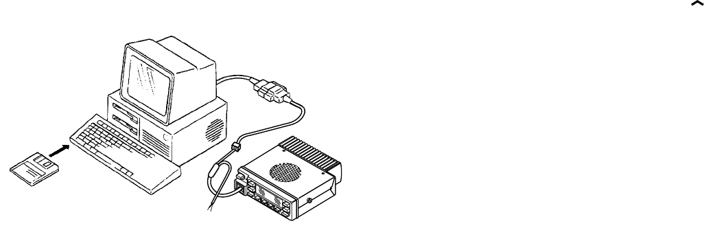
5. PC Mode
5-1. Preface
The TK-760G/762G transceiver is programmed using a
personal computer, a programming interface (KPG-46) and
programming software (KPG-56D).
The programming software can be used with an IBM PC
or compatible. Figure 1 shows the setup of an IBM PC for
programming.
5-2. Connection Procedure
1. Connect the TK-760G/762G to the personal computer
with the interface cable.
2. When the Power is switched on, user mode can be en-
tered immediately. When the PC sends a command, the
radio enters PC mode.
When data is transmitted from transceiver, the red LED
blink.
When data is received by the transceiver, the green LED
blink.
Notes :
• The data stored in the personal computer must match
model type when it is written into the flash memory.
• Change the TK-760G/762G to PC mode, then attach the
interface cable.
5-3. KPG-46 Description
(PC programming interface cable : Option)
The KPG-46 is required to interface the TK-760G/762G to
the computer. It has a circuit in its D-subconnector (25-pin)
case that converts the RS-232C logic level to the TTL level.
The KPG-46 connects the modular microphone jack of
the TK-760G/762G to the computers RS-232C serial port.
KPG-46
IBM-PC
KPG-56D
TK-760G/762G
Fig. 1
12
TK-760G/762G
Note :
You can clone the programmed data between the trans-
ceiver listed below. Frequency version must be same.
Slave
TK-260G TK-260G TK-760G TK-760G TK-760G TK-260G TK-270G
KMKMK2K2M2
TK-270G TK-270G TK-762G TK-762G TK-762G TK-270G
Master K M K M K2 K2
TK-760G YES NO YES NO NO NO NO
K
TK-760G NO YES NO YES NO NO NO
M
TK-760G NO NO NO NO YES YES NO
K2
REALIGNMENT
Cloning cable
(E30-3382-05)
Fig. 2
MBL
PSB
GND
PTT/TXD
ME
MIC
HOOK/RXD
CM
GND
REMOTE/TXD
PTT/RXD
8
1
1
8
Clone cable
E30-3411-05 (TK-760G → TK-260G/270G)
8. Self Programming Mode (TK-760G only)
Write mode for frequency data and signalling etc. Mainly
used by the person maintaining the user equipment.
8-1. Enter to the Self Programming Mode
Remove D507 (Figure 3) from the TX-RX unit. Hold down
the [A] key and turn the power switch on. When enter the
self programming mode, "SELF" is displayed. The mode
changes autoically to Model Select Mode in about one sec-
ond, and set up radio type, radio band & channel type and
frequency version.
Notes :
• To start the Firmware Programmer from KPG-56D, the
FPRO path must be set up by the KPG-56D setup.
• This mode cannot be entered if the Firmware program-
ming mode is set to Disable in the Programming soft-
ware (KPG-56D).
• When programming the firmware, it is recommend to
copy the data from the floppy disk to your hard disk be-
fore you update the radio firmware.
Directly copying from the floppy disk to the radio may not
work because the access speed is too slow.
6-4. Function
1. If you press the [MON] switch while "PROG 576" is dis-
played, the checksum is displayed. If you press the
[MON] switch again (while the checksum is displayed),
"PROG 576" is redisplayed.
2. If you press the [A] switch while "PROG 576" is displayed,
the display changes to "PROG 192" to indicate that the
write speed is low speed (19200 bps). If you press the
[A] switch again while "PROG 192" is displayed, the dis-
play changes to "PROG 384", and the write speed be-
comes the middle speed (38400 bps). If you press the
[A] switch again while "PROG 384" is displayed, the dis-
play returns to "PROG 576".
Note :
TK-762G indicate
19200 bps : The LED flashes green and red alternately.
38400 bps : The LED flashes orange.
57600 bps : The LED lights orange.
Normally, write in the high-speed mode.
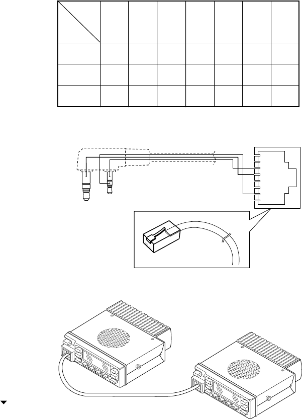
7. Clone Mode
Programming data can be transferred from one radio to
another by connecting them via their modular microphone
jacks. The operation is as follows (the transmit radio is the
master and the receive radio is the slave).
1. Turn the master TK-760G power ON with the [ ] key
held down. The TK-760G displays "CLONE".
2. Power on the slave TK-760G/762G.
3. Connect the cloning cable (No. E30-3382-05) to the
modular microphone jacks on the master and slave.
4. Press the [SCN] key on the master while the master dis-
plays "CLONE". The data of the master is sent to the
slave. While the slave is receiving the data, "–PC–" is dis-
played. When cloning of data is completed, the master
displays "END", and the slave automatically operates in
the User mode. The slave can then be operated by the
same program as the master.
5. The other slave can be continuously cloned. When the
[SCN] key on the master is pressed while the master dis-
plays "END", the master displays "CLONE". Carry out the
operation in step 2 to 4.
13
TK-760G/762G
9. Channel Setting Mode
Each channel can be setup in its action mode by using
the panel keys.
• Pressing [MON] when "SELF" is diaplyed, sets channel
setting mode.
• Select an item set using [ ] then change the selection
with the [CH / ].
• The data displayed using [D/A] is stored in the memory
and then proceeds to the next item.
• Pressing [ ] proceeds to the next item without storing it
in the memory.
• Press [MON] to set the display to "SELF" and return to
reset (default) status.
The setup items fro channel setting mode are listed be-
low.
No. Function
Choices Display Remarks
Select 1~128 __1-__1._ [ ] : Group selection/
channel __1-128._ Channel selection
Select 1~128 __1.-__1_ change
group 128.-__1_
1 RX Step STP__250 Display when an item
frequency
2.5kHz~1MHz STP_1000 is selected or when a
step is changed
(about 0.5 seconds)
[A] : Step change
2.5, 5.0, 6.25, 7.5kHz,
1MHz step
Blank - - - - - - - - [ ] : Frequency on/
100.0000~ R.100.0000 blank switching
550.0000MHz The rightmost dot
indicates 50Hz digit
(On=5, Off=0)
2 RX Off - - - - - - - - [ ] : Off/QT/DQT
signalling
QT 67.0~250.3Hz
QT__67.0_ switching
(EIA mode) QT_250.3_ [A] : Mode switching
QT 67.0~250.3Hz
QT__67.0* [SCN] : Normal/
(0.1Hz step mode)
QT_250.3* Inverse switching
DQT 000~777 DQT000N*
(Normal) DQT777N*
(1 step mode)
DQT 023~754 DQT023N_
(Normal) DQT754N_
(Standard table mode)
DQT 000~777 DQT000I*
(Inverse) DQT777I*
(1 step mode)
DQT 023~754 DQT023I_
(Inverse) DQT754I_
(Standard table mode)
REALIGNMENT
IC502
TX-RX unit B/2
Foil side
50
51
IC505
1
8
4
5
D507
D505
Fig. 3
Note :
This mode (self programming mode) cannot be set when
it has been disabled with the FPU.
[D/A]
[D/A]
[ ]
[D/A]
[MON]
[CH
/ ]
Radio type
Channel set
mode Function set
mode
Self programming mode
Portable Mobile
Radio band &
channel type VHF
8CH VHF
128CH UHF
8CH UHF
128CH
Frequency
version
[CH / ]
[CH
/ ] [CH
/ ]
[CH
/ ]
VHF
F1 VHF
F2 UHF
F1 UHF
F3
[CH / ]
[CH
/ ]
[CH
/ ] [CH
/ ]
UHF
F4
[CH
/ ]
[ ]
Cannot be
set when
portable is
select.
Cannot be
set when
mobile is
select.
*
**
*
8-2. Model Select Mode
• Flow chart
Note :
If the radio type of TK-760G was temporally set to "Por-
table" for the cloning purposes, "UNPROG" is displayed (at
User mode) when the TK-760G is turned on.
In this case, please set the radio type back to "Mobile" at
model select mode menu.
The silk screen of D505 and D507 is reversed on the TX-
RX unit PCB (Part No. J72-0677-02). this silk screen will be
corrected from the next version, J72-0677-12.
14
TK-760G/762G
REALIGNMENT
No. Function
Choices Display Remarks
9 RF High power PWR_H___ ←Default
power Low power PWR_L___
10 Wide/ Wide WIDE____
Narrow Narrow NARROW__
11 Scan DELETE SCAN_DEL Not used for 8ch
Delete/Add
ADD SCAN_ADD ←Default
12 Priority No P.CH_NO__ Not used when (Scan)
channel Yes P.CH_YES_ priority is not fixed
13 Home No H.CH_NO__ Not used when home
channel Yes H.CH_YES_ channel is not set in
key assignment
14
Compander
No COMP_NO_ Not used when wide
is selected
Yes COMP_YES
15 PTT ID OFF P.ID_OFF_
Begin of TX P.ID_1___
End of TX P.ID_2___
Both P.ID_3___
16 Begin 000~ _BOT_ID_ Not valid if Dial ID=
of TX ID
9999999999999999
disable and PTT ID=
off, or EOT is set
Display when an item
is selected (about
0.5 seconds)
12345678 Display of the current
setting (If it is 8 or
more digits, scroll it)
- - - - - 987 Display when a code
is input (Input it with
DTMF key)
Blank - - - - - - - - [ ] : Data clear
17 End of 000~ _EOT_ID_ Not valid of Dial ID=
TX ID
9999999999999999
Idisable and PTT ID=
off, or BOT is set
Display when an item
is selected (about
0.5 seconds)
12345678 Display of the current
setting (If it is 8 or
more digits, scroll it)
- - - - - 987 Display when a code
is input (Input it with
DTMF key)
Blank - - - - - - - - [ ] : Data clear
No. Function
Choices Display Remarks
3 TX Step STP__250 Display when an item
frequency
2.5kHz~1MHz STP_1000 is selected or when a
step is changed
(about 0.5 seconds)
[A] : Step change
2.5, 5.0, 6.25, 7.5kHz,
1MHz step
Blank - - - - - - - - [ ] : Frequency on/
100.0000~ T.100.0000 blank switching
550.0000MHz The rightmost dot
indicates 50Hz digit
(On=5, Off=0)
4 TX Off - - - - - - - - [ ] : Off/QT/DQT
signalling
QT 67.0~250.3Hz
QT__67.0_ switching
(EIA mode) QT_250.3_ [A] : Mode switching
QT 67.0~250.3Hz
QT__67.0* [SCN] : Normal/
(0.1Hz step mode)
QT_250.3* Inverse switching
DQT 000~777 DQT000N*
(Normal) DQT777N*
(1 step mode)
DQT 023~754 DQT023N_
(Normal) DQT754N_
(Standard table mode)
DQT 000~777 DQT000I*
(Inverse) DQT777I*
(1 step mode)
DQT 023~754 DQT023I_
(Inverse) DQT754I_
(Standard table mode)
5 Option Off NONE____ ←Default
signalling
DTMF DTMF____
2-TONE 2TONE___
6 ID 000~ ___ID___ Display when an item
9999999999 is selected (about
0.5 seconds)
12345678 Display of the current
setting (If it is 8 or
more digits, scroll it)
- - - - - 987 Display when a code
is input (Input it with
DTMF key)
Blank - - - - - - - - [ ] : Data clear
7 Busy No BCL_NO__ ←Default
channel Type 1 BCL_1___ BCL_YES_ for K type
lockout Type 2 BCL_2___ Not used for K type
8 Beat No SHFT_NO_ ←Default
shift Yes SHFT_YES
15
TK-760G/762G
10. Function Setting Mode
All channels can be set up together in the action mode by
using the panel keys.
• Pressing [ ] when "SELF" is displayed, sets the function
setting mode.
• Select an item set using [ ] then change the selection
with the [CH /].
• The data displayed using [D/A] is stored in the memory
and then proceeds to the next item.
• Pressing [ ] proceeds to the next item without storing it
in the memory.
• Press [ ] to display "SELF" and return to reset (default)
status.
No. Function
Choices Display Remarks
Function key
1 [MON] Not function MON__OFF
(
TK-760G
Volume down MON___1_
only) Volume up MON___2_
Talk around MON___3_
Auxiliary MON___4_
Dispaly character
MON___5_
Home channel MON___7_
Channel down MON___8_
Channel up MON___9_
Key lock MON___10
Public address MON___12
Horn alert MON___14
Selectable QT MON___15 M destination only
2-tone encode MON___16
select
Monitor A MON___17 ←Default
Monitor B MON___18
Monitor C MON___19
Monitor D MON___20
Scan MON___22
Scan del/add MON___23
Group down MON___24
Group up MON___25
2 [A] No function KEY1_OFF ←Default (TK-760G)
(TK-760G)
Volume down KEY1__1_
[MON] Volume up KEY1__2_
(TK-762G)
Talk around KEY1__3_
Auxiliary KEY1__4_
Dispaly character
KEY1__5_
TK-762G cannot be selected
Home channel KEY1__7_
Channel down KEY1__8_
Channel up KEY1__9_
Key lock KEY1__10
Public address
KEY1__12
REALIGNMENT
9-1. Flow Chart
Self programming
mode
[MON]
[MON] Channel setting
mode Channel selection Group selection
[D/A]
[ ]
OFF QT
OFF
[SCN]
[SCN]
DQT N DQT I
[ ]
[MON]
[MON]
[MON]
[MON]
[MON]
[MON]
[MON]
RX frequency
[D/A]/[ ]
RX signalling
TX freuency
TX signalling
Option signalling
ID
Busy channel lockout
OFF QT
OFF
Data clear
DQT N DQT I
[D/A]/[ ]
[D/A]/[ ]
[D/A]/[ ]
[D/A]/[ ]
[D/A]/[ ]
[MON] Beat shift yes/no
[D/A]/[ ]
[MON] RF power high/low
[D/A]/[ ]
[MON] Wide/Narrow
[D/A]/[ ]
[MON] Scan delete/add
[D/A]/[ ]
[MON] Priority channel Not used when (Scan) priority is not fixed.
Not used when home channel is not set
in key assignment.
Not used when wide is selected.
[D/A]/[ ]
[MON] Home channel
[D/A]/[ ]
[MON] Compander yes/no
[D/A]/[ ]
[MON] PTT ID
[D/A]/[ ]
[MON] Begin of TX ID
[D/A]/[ ]
[MON] End of TX ID
[D/A]/[ ]
[D/A]/[ ]
[ ]
[ ]
[ ]
[ ]
[ ] [ ]
[ ]
[ ]
[ ] [ ]
Data clear
[ ]
Data clear
[ ]
16
TK-760G/762G
No. Function
Choices Display Remarks
Horn alert KEY3__14
Selectable QT KEY3__15 M destination only
TK-762G cannot be selected
2-tone encode KEY3__16
select
Monitor A KEY3__17
Monitor B KEY3__18
Monitor C KEY3__19
Monitor D KEY3__20
Scan KEY3__22
TK-762G cannot be selected
Scan del/add KEY3__23
TK-762G cannot be selected
Group down KEY3__24
TK-762G cannot be selected
Group up KEY3__25
TK-762G cannot be selected
5[] No function KEY4_OFF ←Default
(TK-760G)
Volume down KEY4__1_
[A] Volume up KEY4__2_
(TK-762G)
Talk around KEY4__3_
Auxiliary KEY4__4_
Dispaly character
KEY4__5_
TK-762G cannot be selected
Home channel KEY4__7_
Channel down KEY4__8_
Channel up KEY4__9_
Key lock KEY4__10
Public address KEY4__12
Horn alert KEY4__14
Selectable QT KEY4__15 M destination only
TK-762G cannot be selected
2-tone encode KEY4__16
select
Monitor A KEY4__17
Monitor B KEY4__18
Monitor C KEY4__19
Monitor D KEY4__20
Scan KEY4__22
TK-762G cannot be selected
Scan del/add KEY4__23
TK-762G cannot be selected
Group down KEY4__24
TK-762G cannot be selected
Group up KEY4__25
TK-762G cannot be selected
6 [SCN] No function SCN__OFF ←Default
(TK-760G
Volume down SCN___1_
only) Volume up SCN___2_
Talk around SCN___3_
Auxiliary SCN___4_
Dispaly character
SCN___5_
Home channel SCN___7_
Channel down SCN___8_
Channel up SCN___9_
Key lock SCN___10
REALIGNMENT
No. Function
Choices Display Remarks
Horn alert KEY1__14
Selectable QT
KEY1__15 M destination only
2-tone encode KEY1__16
select
Monitor A KEY1__17 ←Default (TK-762G)
Monitor B KEY1__18
Monitor C KEY1__19
Monitor D KEY1__20
Scan KEY1__22
TK-762G cannot be selected
Scan del/add KEY1__23
TK-762G cannot be selected
Group down KEY1__24
TK-762G cannot be selected
Group up KEY1__25
TK-762G cannot be selected
3 [D/A] No function KEY2_OFF ←Default
(TK-760G)
Volume down KEY2__1_
[] Volume up KEY2__2_
(TK-762G)
Talk around KEY2__3_
Auxiliary KEY2__4_
Dispaly character
KEY2__5_
TK-762G cannot be selected
Home channel
KEY2__7_
Channel down
KEY2__8_
Channel up KEY2__9_
Key lock KEY2__10
Public address
KEY2__12
Horn alert KEY2__14
Selectable QT KEY2__15 M destination only
TK-762G cannot be selected
2-tone encode KEY2__16
select
Monitor A KEY2__17
Monitor B KEY2__18
Monitor C KEY2__19
Monitor D KEY2__20
Scan KEY2__22
TK-762G cannot be selected
Scan del/add KEY2__23
TK-762G cannot be selected
Group down KEY2__24
TK-762G cannot be selected
Group up KEY2__25
TK-762G cannot be selected
4[] No function KEY3_OFF ←Default
(TK-760G)
Volume down KEY3__1_
[] Volume up KEY3__2_
(TK-762G)
Talk around KEY3__3_
Auxiliary KEY3__4_
Dispaly character
KEY3__5_
TK-762G cannot be selected
Home channel
KEY3__7_
Channel down KEY3__8_
Channel up KEY3__9_
Key lock KEY3__10
Public address KEY3__12
17
TK-760G/762G
No. Function
Choices Display Remarks
Public address
CUP___12
Horn alert CUP___14
Selectable QT CUP___15 M destination only
TK-762G cannot be selected
2-tone encode CUP___16
select
Monitor A CUP___17
Monitor B CUP___18
Monitor C CUP___19
Monitor D CUP___20
Scan CUP___22
TK-762G cannot be selected
Scan del/add CUP___23
TK-762G cannot be selected
Group down CUP___24
TK-762G cannot be selected
Group up CUP___25
TK-762G cannot be selected
9 [CH ] No function CDN__OFF
(
Channel
Volume down CDN___1_
down) Volume up CDN___2_
Talk around CDN___3_
Auxiliary CDN___4_
Dispaly character
CDN___5_
TK-762G cannot be selected
Home channel
CDN___7_
Channel down
CDN___8_ ←Default
Channel up CDN___9_
Key lock CDN___10
Public address
CDN___12
Horn alert CDN___14
Selectable QT CDN___15 M destination only
TK-762G cannot be selected
2-tone encode CDN___16
select
Monitor A CDN___17
Monitor B CDN___18
Monitor C CDN___19
Monitor D CDN___20
Scan CDN___22
TK-762G cannot be selected
Scan del/add CDN___23
TK-762G cannot be selected
Group down CDN___24
TK-762G cannot be selected
Group up CDN___25
TK-762G cannot be selected
10 [VOL ] No function VUP__OFF
(
Volume
Volume down VUP___1_
up) Volume up VUP___2_ ←Default
Talk around VUP___3_
Auxiliary VUP___4_
Dispaly character
VUP___5_
TK-762G cannot be selected
Home channel
VUP___7_
Channel down
VUP___8_
Channel up VUP___9_
REALIGNMENT
No. Function
Choices Display Remarks
Public address SCN___12
Horn alert SCN___14
Selectable QT SCN___15 M destination only
2-tone encode SCN___16
select
Monitor A SCN___17
Monitor B SCN___18
Monitor C SCN___19
Monitor D SCN___20
Scan SCN___22
Scan del/add SCN___23
Group down SCN___24
Group up SCN___25
7 [FOOT] No function FSW__OFF ←Default
(FOOT Volume down FSW___1_
SW) Volume up FSW___2_
Talk around FSW___3_
Auxiliary FSW___4_
Dispaly character
FSW___5_
Emergency FSW___6_
Home channel FSW___7_
Channel down FSW___8_
Channel up FSW___9_
Key lock FSW___10
Public address FSW___12
Horn alert FSW___14
Selectable QT FSW___15 M destination only
2-tone encode FSW___16
select
Monitor A FSW___17
Monitor B FSW___18
Monitor C FSW___19
Monitor D FSW___20
Scan FSW___22
Scan del/add FSW___23
Group down FSW___24
Group up FSW___25
8 [CH ] No function CUP__OFF
(
Channel
Volume down CUP___1_
up) Volume up CUP___2_
Talk around CUP___3_
Auxiliary CUP___4_
Dispaly character
CUP___5_
TK-762G cannot be selected
Home channel
CUP___7_
Channel down
CUP___8_
Channel up CUP___9_ ←Default
Key lock CUP___10

18
TK-760G/762G
No. Function
Choices Display Remarks
15
Minimum
0~31/1 step MVOL_12_
volume
16
Off hook
Enable H_D__ENA
decode Disable H_D__DIS ←Default
17
Off hook
Enable H_H__ENA
horn alert
Disable H_H__DIS ←Default
18
Time out
OFF, 15~600/ TOT_180_ Default : 180s
timer 15s step
19 TOT OFF, 1~10/ TOTP_OFF Cannot be set when
pre-alert
1s step TOT is off
time Default : Off
20 TOT OFF, 1~60/ TOTK_OFF Cannot be set when
rekey 1s step TOT is off
time Default : Off
21 TOT OFF, 1~15/ TOTS_OFF Cannot be set when
reset 1s step TOT is off
time
22 Clear to YES CTT_YES_
transpond
NO CTT_NO__ ←Default
(BCL for
transpond)
23
Signalling
OR SIG__OR_ ←Default
AND SIG__AND
24 Squelch 0~9/1 step SQL__5__ Default : 5
level
Scan
25 Priority None PRI_NONE Default : None
Fixed PRI_FIX_
Selected PRI_SEL_
26 Look 0.5~5.0/ LBA__500 Default : 500ms
back 0.05s Cannot be set when
time A Priority=none
27 Look 0.5~5.0/ LBB_2000 Default : 2000ms
back 0.05s Cannot be set when
time B Priority=none
28 Revert Selected REV_SEL_
channel Last called REV_L/C_ ←Default
Last used REV_L/U_
Selected+Talk back
REV_S/T_
Priority REV_PRI_
Priority+Talk back
REV_P/T_
29 Dropout 0~300/1s DODT___3 Default : 3s
delay time
30
Dwell time
0~300/1s DWL____3 Default : 3s
31
Off hook
Enable H_S__ENA
scan Disable H_S__DIS ←Default
REALIGNMENT
No. Function
Choices Display Remarks
Key lock VUP___10
Public address
VUP___12
Horn alert VUP___14
Selectable QT
VUP___15 M destination only
TK-762G cannot be selected
2-tone encode VUP___16
select
Monitor A VUP___17
Monitor B VUP___18
Monitor C VUP___19
Monitor D VUP___20
Scan VUP___22
TK-762G cannot be selected
Scan del/add VUP___23
TK-762G cannot be selected
Group down VUP___24
TK-762G cannot be selected
Group up VUP___25
TK-762G cannot be selected
11 [VOL ] No function VDN__OFF
(
Volume
Volume down VDN___1_ ←Default
down) Volume up VDN___2_
Talk around VDN___3_
Auxiliary VDN___4_
Dispaly character
VDN___5_
TK-762G cannot be selected
Home channel
VDN___7_
Channel down
VDN___8_
Channel up VDN___9_
Key lock VDN___10
Public address
VDN___12
Horn alert VDN___14
Selectable QT
VDN___15 M destination only
TK-762G cannot be selected
2-tone encode VDN___16
select
Monitor A VDN___17
Monitor B VDN___18
Monitor C VDN___19
Monitor D VDN___20
Scan VDN___22
TK-762G cannot be selected
Scan del/add VDN___23
TK-762G cannot be selected
Group down VDN___24
TK-762G cannot be selected
Group up VDN___25
TK-762G cannot be selected
Optional feature
12 Power YES/NO PONT_YES Default : Yes
on tone
13 Control YES/NO CNTT_YES Default : Yes
tone
14 Warning YES/NO WART_YES Default : Yes
tone
19
TK-760G/762G
REALIGNMENT
Self programming
mode
Function setting
mode
[MON] key function
[D/A]/[ ]
[A]/[MON] key function
[D/A]/[ ] key function
[ ]/[ ] key function
[ ]/[A] key function
[SCN] key function
[FOOT] key function
[D/A]/[ ]
[D/A]/[ ]
[D/A]/[ ]
[D/A]/[ ]
[D/A]/[ ]
[CH ] key function
[D/A]/[ ]
[CH ] key function
[D/A]/[ ]
[VOL ] key function
[D/A]/[ ]
[VOL ] key function
[D/A]/[ ]
Power on tone yes/no
[D/A]/[ ]
Control tone yes/no
[D/A]/[ ]
Warning tone yes/no
[D/A]/[ ]
Minimum volume
[D/A]/[ ]
Off hook decode
[D/A]/[ ]
Off hook horn alert
[D/A]/[ ]
[D/A]/[ ]
Time out timer
TOT pre-alert time
[D/A]/[ ]
TOT rekey time
[D/A]/[ ]
TOT reset time
[D/A]/[ ]
Clear to transpond
[D/A]/[ ]
Signalling
[D/A]/[ ]
[D/A]/[ ]
[ ]
[ ]
[ ]
[ ]
[ ]
[ ]
[ ]
[ ]
[ ]
[ ]
[ ]
[ ]
[ ]
[ ]
[ ]
[ ]
[ ]
[ ]
[ ]
[ ]
[ ]
[ ]
[ ]
[ ]
[ ]
Look back time A
Priority
Squelch level
[D/A]/[ ]
Look back time B
Revert channel
Dropout delay time
Dwell time
Off hook scan
Digit time
[D/A]/[ ]
[D/A]/[ ]
[D/A]/[ ]
[D/A]/[ ]
[D/A]/[ ]
[D/A]/[ ]
[D/A]/[ ]
Inter digit time
[D/A]/[ ]
First digit time
[D/A]/[ ]
First digit delay
[D/A]/[ ]
Rise time with QT
[D/A]/[ ]
Dial ID
[D/A]/[ ]
No. of DTMF key
[D/A]/[ ]
DTMF hold time
[D/A]/[ ]
Store & Send
[D/A]/[ ]
D key assignment
[D/A]/[ ]
DTMF signalling
[D/A]/[ ]
[D/A]/[ ]
Inter mediate code
Group code
[D/A]/[ ]
Auto reset time
[D/A]/[ ]
Call alert/Transpond
[D/A]/[ ]
Panel test/
Panel tuning mode
[D/A]/[ ]
[ ]
[ ]
[ ]
[ ]
[ ]
[ ]
[ ]
[ ]
[ ]
[ ]
[ ]
[ ]
[ ]
[ ]
[ ]
[ ]
[ ]
[ ]
[ ]
[ ]
[ ]
[ ]
[ ]
[ ]
No. Function
Choices Display Remarks
DTMF
32
Digit time
50~200ms/10ms
DIGT__50 Default : 50ms
33
Inter digit
50~1000ms/50ms
IDT___50 Default : 50ms
time
34
First digit
50~200ms/10ms
FDT___50 Default : 50ms
time
35
First digit
50~1000ms/50ms
RIST_100 Default : 100ms
delay
36
Rise time
50~1000ms/50ms
RTWQ_100 Default : 100ms
with QT
37 Dial ID Enable DID__ENA
Disable DID__DIS ←Default
38 No. of 12 key NODK_12_ ←Default
DTMF key
16 key NODK_16_
39 DTMF ON DHT__ON_ ←Default
hold time
OFF DHT__OFF
40
Store and
Enable SAS__ENA
send Disable SAS__DIS ←Default
41 D key D code DKA_D_CD ←Default
assignment
1~16s/1s DKA_16__
42 DTMF Code SQ DTMS_CSQ ←Default
signalling
SWL CALL DTMF_SEL TK-760G only
43 Inter 0~9, A~D, IMC__#__ Default : # (Can be
mediate *, # set only when DTMF
code signalling=SEL CALL)
44 Group A~D, *, # GPCD_OFF Default : OFF
code
45 Auto OFF ART__OFF
reset time
1~15s/1s ART__10_ Default : 10s
46
Call alert
OFF CA/T_OFF ←Default
/transpond
Call alert CA/T_C/A
Transpond CA/T_T/A
(Call alert)
Transpond CA/T_T/I
(ID code)
Transpond CA/T_T/T
(Transpond code)
Others
47 Panel Enable PTM__ENA ←Default
test/ Not used for TK-762G
panel Disable PTM__DIS
tuning
mode
10-1. Flow Chart
11. Memory Reset Mode (TK-760G only)
You can clear all settings you made in self programming
mode, or you can return to the original display.
• Press [SCN] while "SELF" is displayed will change the dis-
play to "CANCEL".
• Press [CH /] to change the display between "CAN-
CEL" and "READY".
• When "READY" is displayed, pressing [SCN] will set all
data to default, and "CLEAR" will appear on the display.
Press [SCN] again to display "SELF".
• When "CANCEL" is displayed, pressing [SCN] will cancel
the reset, and "SELF" will be displayed.
20
TK-760G/762G
34
5
6
7
8 9
1. Accessory Connection Cable
(KCT-19 : Option)
The KCT-19 is an accessory connection cable for con-
necting external equipment. The connector has 15 pins and
the necessary signal lines are selected for use.
1-1. Installing the KCT-19 in the transceiver
1. Remove the upper and lower halves of the transceiver
case, and lift the DC cord bushing ( ) from the chassis.
2. Remove the pad as shown in Figure 1 ( ).
3. Insert the KCT-19 cable ( ) into the chassis ( ).
The wire harness band ( ) must be inside the chassis.
4. Replace the DC cord bushing ( ).
5. Connect the KCT-19 to the TX-RX unit (A/2) as shown in
Figure 2 ( ).
6. Connect the KCT-19 to the external accessory by insert-
ing the crimp terminal ( ) into the square plug ( ),
both of which are supplied with the KCT-19.
1
2
1
3
13
15 12
Crimp terminal
(E23-0613-05)
B
E
C
B
D
CN8
CN5
D
E
B
C
A
Contact
Square plug
(E09-1571-05)
3
4
6
7
8
9
5
CN4
CN3
1
2
Fig. 1
Fig. 2
INSTALLATION
1-2. KCT-19 Accessory Port Function
No. No. Name Function
Note
(A)
(B,C,D,E)
1 D-2 RXD Serial control data input *1
DTC Data channel control/ *2
External hook input
2 D-5 ME External microphone ground
3 D-3 IGN Ignition sense input
4 D-1 DEO Receiver detector output
5 D-6 MI External microphone input
6 B-2 E Ground
7 B-3 SB Switched B+, DC 13.6V output.
Maximum 1A
8 D-7 PTT External PTT input *2
9 D-4 DI Data modulation input
10 B-1 HOR Horn alert/call output
11 D-8 SQ Squelch detect output Busy : H *2
12 C-1 SP Speaker audio output.
13 E-1 AM
Speaker mute input, active high
14 E-2 MM MIC mute input, active high
15 E-3 EMG Foot switch input, active low *3
TXS
Transmitter sense output, active high
*1 : SmarTrunk OMNI mode
*2 : MDT mode
*3 : Emergency mode
21
TK-760G/762G
INSTALLATION
2. Accessory Terminal (TX-RX Unit)
2-1. External Connector Accessory Terminal Method
No. Name I/O Description Note
CN1 1 8C O DC 8V output
2 5S O DC 5V output
3 AUX5 O SMRD : Reset output *1
4 AUX6 O
5SC : 5S control (Cannot use)
*1
5 NC – Non-connection
6 AUX3 O SQ : Squelch detect output *2
7 AUX1 I PTT : External PTT input *2
8 AUX4 TXD
TXD : Serial control data output
*1
9 AUX2 RXD
RXD : Serial control data input
*1
I DTC : Data channel control/
External hook input
I CHDATA : Channel control
serial data input
10 ALT I Alert tone input
11 AFO O Receiver audio signal output
12 AFI I Receiver audio signal input
13 MII I Transmit audio signal input
14 MIO O Transmit audio signal output
15 GND – Ground
CN3 1 HOR O Horn alert/call output
2 E – Ground
3 SB O Switched B+, DC 13.6V
output, Maximum 1A
CN4 1 DEO O Receiver detector output
Level : 0.5Vrms
(Standard modulation)
2 DTC I Data channel control/
External hook input
3 IGN I Ignition sense input
4 DI I Data modulation input
5 ME – External microphone ground
6 MI I External microphone input
7 PTT I
External PTT input, active low
8 SQ O Squelch detect output
CN5 1 AM I
Speaker mute input, active high
2 MM I MIC mute input, active high
3 EMG/TXS I EMG : Foot switch input, *3
active low
CN7 1 PA/LI O Relay for PA function KAP-1
control
O
PA/LI ON : High, PA/LI OFF : Low
2 SPO O Audio signal output to KAP-1
3 SPI I
Audio signal input from KAP-1
CN8 1 SP O Audio signal output to
internal/external speaker
2 E – Ground
*1 : SmarTrunk OMNI mode
*2 : MDT mode
*3 : Emergency mode
3. Ignition Sense Cable (KCT-18 : Option)
The KCT-18 is an optional cable for enabling the ignition
function. The ignition function lets you turn the power to the
transceiver on and off with the car ignition key.
If you use the Horn Alert function or the Manual Relay
function, you can turn the function off while driving with the
ignition key.
3-1. Connecting the KCT-18 to the Transceiver
1. Install the KCT-19 in the transceiver. (See the KCT-19
section.)
2. Insert the KCT-18 lead terminal ( ) into pin 3 of the
square plug ( ) supplied with the KCT-19, then insert
the square plug into the KCT-19 connector ( ).
2
1
3
1
3
6
13
15
KCT-18
KCT-19
Contact
12
3
Fig. 3

22
TK-760G/762G
INSTALLATION
3-2. Modifying the Transceiver
Modify the transceiver as follows to turn the power or
the Horn Alert or Manual Relay function on and off with the
ignition key.
1. Remove the lower half of the transceiver case.
2. Set jumper resistors (0Ω) R134 and R135 of the TX-RX
unit (A/2) as shown in Table 1.
TX-RX UNIT
(A/2)
ANT
KCT-19
CN2
R134
R133
R135
Fig. 4
Operation when KCT-18 R134 R135
is connected
Enable Enable ← KCT-18 cannot
Power on/off and Horn Disable Enable be connected
Alert or AUX-A on/off
Horn Alert or AUX-A Enable Disable
on/off
Disable Disable ← Power cannot
be turned on
Table 1 R134 and R135 setup chart
2
3
4
1
3
W1
W2
CN1
CN2
KCT-19
Cushion
(G13-1710-04)
CN3
CN7
1
CN3
Fig. 5
4. PA/HA Unit (KAP-1 : Option)
4-1. Installing the KAP-1 in the Transceiver
The Horn Alert (max. 2A drive) and Public Address func-
tions are enabled by inserting the KAP-1 W1 (3P; white/
black/red) into CN3 on the TX-RX unit, inserting W2 (3P;
green) into CN7 on the TX-RX unit, and connecting the KCT-
19 (option) to CN2 and CN3 of the KAP-1.
•Installation procedure
1. Open the upper case of the transceiver.
2. Insert the two cables ( ) with connectors from the
KAP-1 switch unit into the connectors on the transceiver.
3. Secure the switch unit board to the chassis with a screw
( ). The notch ( ) in the board must be placed at the
front left side.
4. Attach the cushion on the top of the KAP-1 switch unit.
1
32
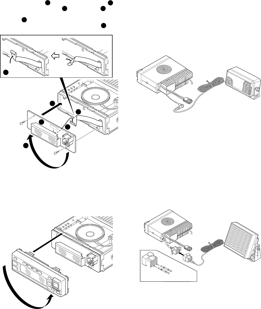
5. Fitting the Control Panel Upside Down
The TK-760G/762G control panel can be fitted upside
down, so the transceiver can be mounted with its internal
speaker (in the upper half of the case) facing down in your
car.
1. Remove the control panel and the TX-RX unit (B/2) con-
trol section. (Fig. 6)
Fig. 6
23
TK-760G/762G
INSTALLATION
12
3 4
5
6
2. Fold the flat cable ( ) in the opposite direction ( ).
3. Rotate the control section ( ) 180 degrees ( ).
4. Insert the flat cable into the control section connector,
CN501 ( ).
5. Mount the control section on the transceiver ( ).
CN501
1
2
3
4
5
6
Fig. 7
6. External Speaker
6-1. KES-3 : Option
The KES-3 is an external speaker for the 3.5-mm-diam-
eter speaker jack.
•Connection procedure
1. Connect the KES-3 to the 3.5-mm-diameter speaker jack
on the rear of the transceiver.
KES-3
Fig. 9
6. Rotate the control panel 180 degrees and mount it on the
transceiver. Refit the two halves of the case to complete
installation. (Fig. 8)
Fig. 8
6-2. KES-4 : Option
The KES-4 is an external speaker used with the acces-
sory connection cable.
•Connection procedure
1. Install the KCT-19 in the transceiver. (See the KCT-19
section.)
2. Insert the crimp terminal into the square plug supplied
with the KCT-19.
3. Connect CN8 of the transceiver to connector C of the
KCT-19 instead of to the internal speaker connector.
KES-4
1
36
13
15
12
Crimp terminal
(E23-0613-05)
Black lead
Black/White lead
Fig. 10
24
TK-760G/762G
Frequency Configuration
The receiver utilizes double conversion. The first IF is
49.95MHz and the second IF is 450kHz. The first local oscil-
lator signal is supplied from the PLL circuit.
The PLL circuit in the transmitter generates the neces-
sary frequencies. Figure 1 shows the frequencies.
Fig. 1 Frequency configuration
Receiver System
The receiver is double conversion superheterodyne. The
frequency configuration is shown in Figure 1.
■Front-end RF Amplifier
An incoming signal from the antenna is applied to an RF
amplifier (Q27) after passing through a transmit/receive
switch circuit (D33 and D34 are off) and a band pass filter
(L18). After the signal is amplified (Q27), the signal is fil-
tered through a band pass filter (L11, L13 and L15) to elimi-
nate unwanted signals before it is passed to the first mixer.
Band pass filters (L18, L11, L13 and L15) have varactor di-
odes (D30, D31, D18, D23 and D28).
The voltage of these diodes are controlled by to track the
CPU (IC502) center frequency of the band pass filter. (See
Fig. 2)
■First Mixer
The signal from the RF amplifier is heterodyned with the
first local oscillator signal from the PLL frequency synthe-
sizer circuit at the first mixer (Q15) to create a 49.95MHz
first intermediate frequency (1st IF) signal. The first IF signal
is then fed through two monolithic crystal filters (MCFs :
XF1) to further remove spurious signals.
■IF Amplifier
The first IF signal is amplified by Q13, and the enters IC5
(FM processing IC). The signal is heterodyned again with a
second local oscillator signal within IC5 to create a 450kHz
second IF signal. The second IF signal is then fed through a
450kHz ceramic filter (Narrow : CF1, Wide : CF2) to further
eliminate unwanted signals before it si amplified and FM
detected in IC5.
Item Rating
Nominal center frequency 49.95MHz
Pass bandwidth ±5.0kHz or more at 3dB
35dB stop bandwidth ±20.0kHz or less
Ripple 1.0dB or less
Insertion loss 5.0dB or less
Guaranteed attenuation 80dB or more at fo±1MHz
Spurious : 40dB or more within fo±1MHz
Terminal impedance 350Ω±5% / 5.5pF±0.5pF
Table 1 Crystal filter (L71-0551-15) : XF1
Item Rating
Nominal center frequency 450kHz
6dB bandwidth ±4.5kHz or more
50dB bandwidth ±10.0kHz or less
Ripple 2.0dB or less
Insertion loss 6.0dB or less
Guaranteed attenuation 55.0dB or more within fo±100kHz
Terminal impedance 2.0kΩ
Table 2 Ceramic filter (L71-0959-05) : CF1
Item Rating
Nominal center frequency 450kHz
6dB bandwidth ±6.0kHz or more
50dB bandwidth ±12.5kHz or less
Ripple 3.0dB or less
Insertion loss 6.0dB or less
Guaranteed attenuation 35.0dB or more within fo±100kHz
Terminal impedance 2.0kΩ
Table 3 Ceramic filter (L72-0973-05) : CF2
Fig. 2 Receiver system
CIRCUIT DESCRIPTION
ANT
SW
RF
AMP
1st
MIX
AF
AMP
TCXO
MIC
AMP
X3
multiply
TX
AMP
PA
AMP
CF 450kHz
MCF
49.95MHz
IF SYSTEM
PLL/VCO
16.8MHz
50.4MHz
ANT
RX
TX
SP
MIC
1/2
ANT
L18
BPF
L11,13,15
BPF
Q27
RF AMP
Q13
IF AMP
IC4
AF AMP
Q15
MIX
XF1
MCF
D33,34
ANT
SW
IC8
1/2 divider
IC6
D/A
Q7
X3 multiply
X1
VCXO
IC5
MIX,IF,DET
1st local
OSC (PLL)
DEO
CF1 (Narrow)
CF2 (Wide)
APC TUNE
CPU Q35
Wide/
Narrow SW
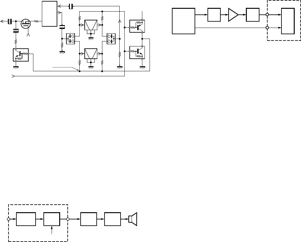
25
TK-760G/762G
■Wide/Narrow Changeover Circuit
The W/N port (pin 4) of the shift register (IC510) is used
to switch between ceramic filters. When the W/N port is
high, Q4 turns on and the ceramic filter SW diode (D8, D10)
CF1 turns on to receive a Narrow signal. At the same time,
Q35 turns on and one of the filters is selected so that the
wide and narrow audio output levels are equal.
When the W/N port is low, Q3 turns on and the ceramic
filter SW diode (D8, D10) CF2 turns on to receive a Wide
signal.
■AF Signal System
The detection signal (DEO) from the TX-RX unit goes to
the audio processor (IC508) of the control unit. The signal
passes through a filter in the audio processor to adjust the
gain, and is output to IC507. IC507 sums the AF signal and
the DTMF signal, BEEP signal and returns the resulting sig-
nal to the TX-RX unit. The signal (AFO) sent to the TX-RX
unit is input to the D/A converter (IC6). The AFO output level
is adjusted by the D/A converter. The signal output from the
D/A converter is input to the audio power amplifier (IC13).
The AF signal from IC13 switches between the internal
speaker and speaker jack (J1) output.
■Squelch Circuit
The detection output from the FM IF IC (IC5) passes
through a band-pass filter and a noise amplifier (Q10) in the
control unit to detect noise. A voltage is applied to the CPU
(IC502). The CPU controls squelch according to the voltage
(ASQ) level. The signal from the RSSI pin of IC5 is moni-
tored. The electric field strength of the receive signal can be
known before the ASQ voltage is input to the CPU, and the
scan stop speed is improved.
FIg. 4 AF signal system
Fig. 5 Squelch circuit
CIRCUIT DESCRIPTION
Fig. 3 Wide/Narrow changeover circuit
CF1
(Narrow)
CF2
(Wide)
IFI
MXO
IC5
IF system
AFO
DET
OUT
C70
C72
C53
R19
R23
R46
R32 R30
R39
R38
+
+
Q35
8RC
Q37 R59
W/N
IC510 4pin
Wide : L
Narrow : H
C51
D8 D10
Q3
5C
Q4
Wide : H
Narrow : L
AUDIO
PROCE.
SUM
AMP
D/A
CONV.
IC508 IC507 IC6
AF PA
IC13 SP
DTMF
AFO
DEO
CONTORL UNIT
Q10
NOISE AMP
D11IC4IC5 IC502
AF
RSSI
BPF DET
CPU
IF
SYSTEM
CONTROL UNIT
ASQ
RSSI
PLL Frequency Synthesizer
The PLL circuit generates the first local oscillator signal
for reception and the RF signal for transmission.
■PLL
The frequency step of the PLL circuit is 5 or 6.25kHz. A
16.8MHz reference oscillator signal is divided at IC3 by a
fixed counter to produce the 5 or 6.25kHz reference fre-
quency. The voltage controlled oscillator (VCO) output sig-
nal is buffer amplified by Q106 (Sub-unit), then divided in IC3
by a dual-module programmable counter. The divided signal
is compared in phase with the 5 or 6.25kHz reference signal
in the phase comparator in IC3. The output signal from the
phase comparator is filtered through a low-pass filter and
passed to the VCO to control the oscillator frequency. (See
Fig. 6)
■VCO
The TK-760G/762G has VCO in a Sub-unit (A1) housed in
a solid shielded case and connected to the TX-RX unit
through CN101.
The operating frequency is generated by Q103 in trans-
mit mode and Q101 in receive mode. The oscillator fre-
quency is controlled by applying the VCO control voltage,
obtained from the phase comparator, to the varactor diodes
(D102 and D104 in transmit mode and D101 and D103 in
receive mode). The RX (ST) pin is set low in receive mode
causing Q102 to turn Q103 off, and turn Q101 on. The RX
(ST) pin is set low in transmit mode. The outputs from Q101
and Q103 are amplified by Q106 and sent to the buffer am-
plifiers.
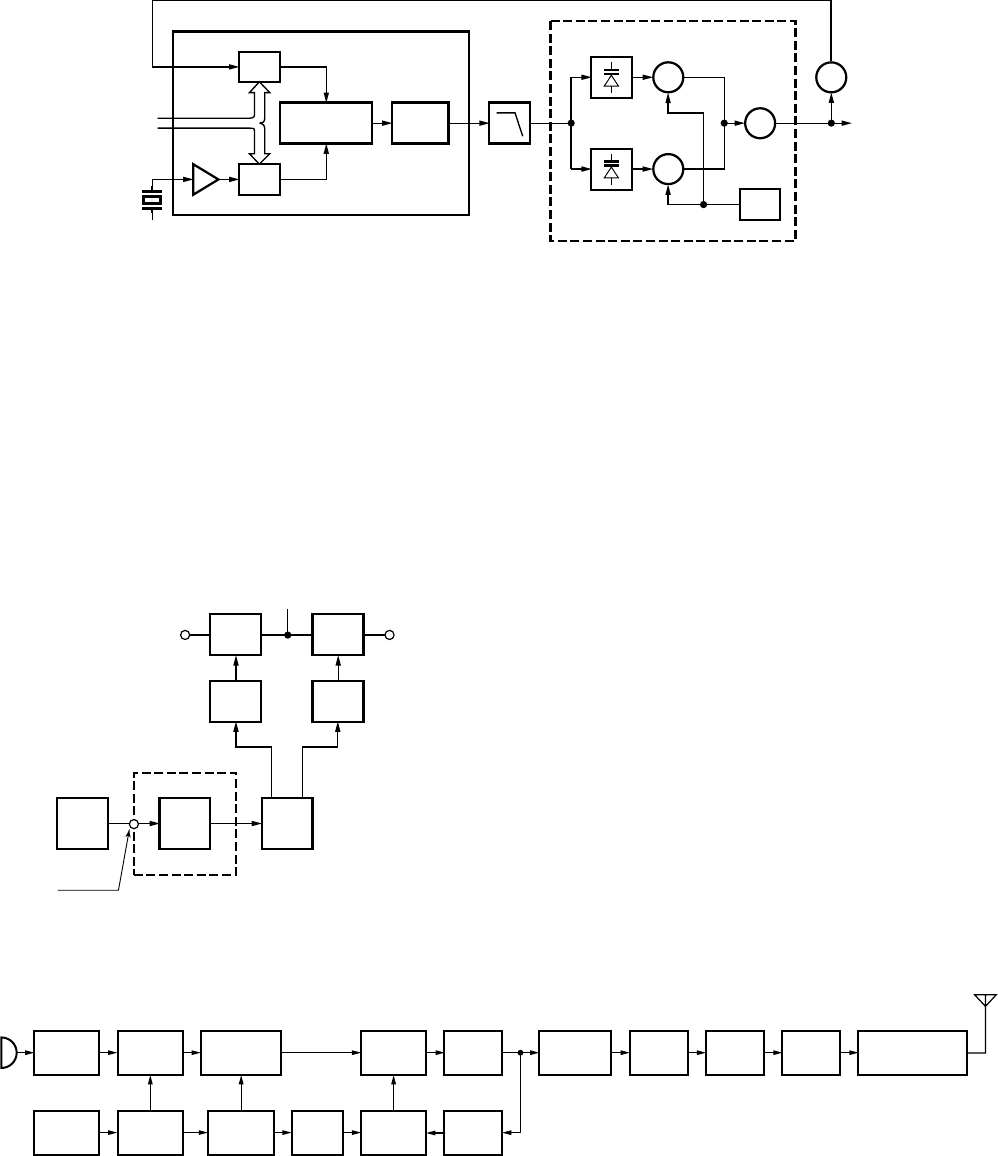
26
TK-760G/762G
D102,104
Q103
TX VCO
Q106
BUFF
AMP
D101,103
Q101
RX VCO Q102,
104,105
T/R SW
Charge
pump
LPF
Phase
comparator
1/M
1/N
PLL/VCO
5kHz/6.25kHz
5kHz/6.25kHz
REF
OSC
16.8MHz
PLL
DATA
IC3 : PLL IC
Q9
RF AMP
Fig. 6 PLL circuit
■Unlock Circuit
During reception, the 8RC signal goes high, the 8TC sig-
nal goes low, and Q16 turns on. Q18 turns on and a voltage
is applied to the collector (8R). During transmission, the
8RC signal goes low, the 8TC signal goes high and Q29
turns on. Q28 turns on and a voltage is applied to 8T.
The CPU in the control unit monitors the PLL (IC3) LD
signal directly. When the PLL is unlocked during transmis-
sion, the PLL LD signal goes low. The CPU detects this
signal and makes the 8TC signal low. When the 8TC signal
goes low, no voltage is applied to 8T, and no signal is trans-
mitted.
IC9
SHIFT
REG.
IC502
CPU
Q16
SW
Q18
SW
IC3
PLL
Q29
SW
Q28
SW
LD
CONTORL UNIT
8RC
8C
8R 8T
8TC
PLL lock
: LD "H"
Fig. 7 Unlock circuit
IC508 IC6 Q103IC507(1/2)MIC
AF AMP
NJM2904V
MIC KEY
INPUT
AF AMP,
IDC, LPF
TC35453F
IC502
CPU
30622M
4XXXGP
D/A
CONVERTER
M62363FP
IC1
SUM AMP
TA75S01F
X1
VCXO
16.8MHz
VCO
2SK508NV
(K52)
IC3
PLL
MB15A02
Q106
BUFFER
2SC4226
(R24)
Q9
BUFFER
2SC4215
(Y)
Q22
RF AMP
2SC3357
Q25
ANT
RF AMP
2SC2954
IC400
POWER AMP
M67741H-32 : K,M
M67741L-35 : K2
Q14
BUFFER
2SC4649
(N,P)
IC8
1/2
DIVIDER
UPB1509GV
Fig. 8 Transmitter system
Transmitter System
■Outline
The transmitter circuit produces and amplifies the de-
sired frequency directly. It FM-modulates the carrier signal
by means of a varicap diode
■Power Amplifier Circuit
The transmit output signal from the VCO is amplified to a
specified level of the power module (IC400) by the drive
block (Q22 and Q25). The amplified signal passes through
the transmission/reception selection diode (D16) and goes
to a low-pass filter. The low-pass filter removes unwanted
high-frequency harmonic components, and the resulting sig-
nal is goes the antenna terminal.
CIRCUIT DESCRIPTION
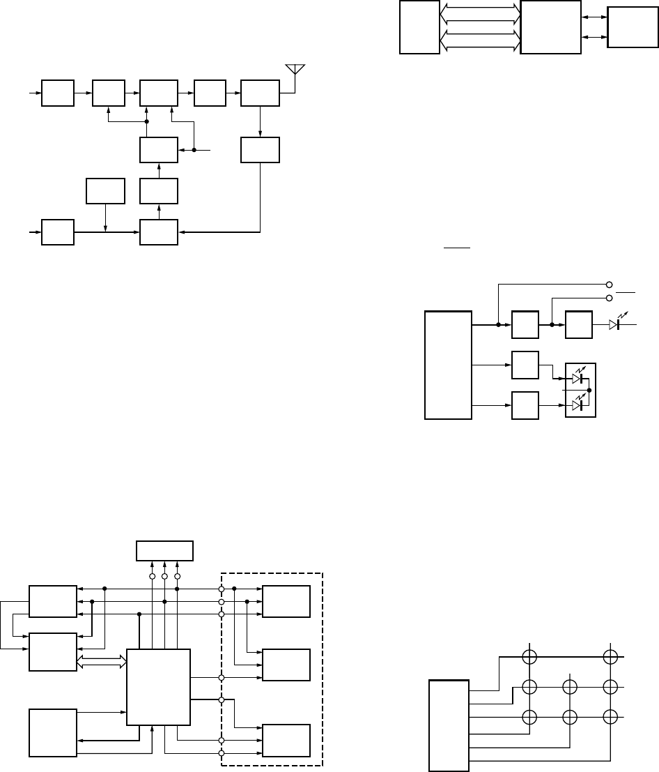
27
TK-760G/762G
■APC Circuit
The automatic transmission power control (APC) circuit
detects part of a power module output with a diode (D35,
D36) and applies a voltage to IC15. IC15 compares the APC
control voltage (PC) generated by the D/A converter (IC6)
and DC amplifier (IC7) with the detection output voltage to
control Q31 and Q32, generates DB voltage from B voltage,
and stabilizes transmission output.
The APC circuit is configured to protect over current of
the power module due to fluctuations of the load at the an-
tenna end and to stabilize transmission output at voltage
and temperature variations.
■Memory Circuit
The transceiver has a 2M-bit (256k x 8) flash ROM
(IC501) and an 8k-bit EEPROM (IC505). The flash ROM con-
tains firmware programs, data and user data which is pro-
grammed with the FPU. The EEPROM contains adjustment
data. The CPU (IC502) controls the flash ROM through an
external address bus and an external data bus. The CPU
controls the EEPROM through two serial data lines.
Control Circuit
The CPU carries out the following tasks:
1) Controls the shift register (IC9, IC510) AF MUTE, WIDE/
NARROW, T/R KEY outputs.
2) Adjusts the AF signal level of the audio processor (IC508)
and turns the filter select compounder on or off.
3) Controls the DTMF decoder (IC511).
4) Controls the LCD assembly display data.
5) Controls the PLL (IC3).
6) Controls the D/A converter (IC6) and adjusts the volume,
modulation and transmission power.
Fig. 9 APC circuit
Fig. 10 Control circuit
Fig. 11 Memory circuit
CIRCUIT DESCRIPTION
RF
AMP
Q22
RF
AMP
Q25
POWER
AMP
IC400
APC
DRIVER
Q32
DB
+B
Q31
PRI
DRIVER
DC
AMP
IC7
ANT
SW
D34
LPF
ANT
POWER
DET
D35,36
IC15
APC
CONTROL
D16
PC
IC6
23pin
Q33
TEMP
PROTECT
IC6
D/A
converter
IC3
PLL
IC9
Shift
register
IC510
Shift
register
OE
LCDCS
CNTCK
CNTDT
AFCLR
AFMSKE
AFSTB
IC508
Audio
processor
IC511
DTMF
DECO.
IC502
CPU
TX-RX UNIT
LCD ASSY
AFREG2
AFREG1
DTMDAT
DTMCLK
DTMSTD
DAST
PLST
PLDT
PLCK
SCL
SDA
IC502
CPU
ADDRESS BUS
DATA BUS
IC501
FLASH
ROM
IC505
EEPROM
Q506
SW
Q508
SW
Q504
SW
Q505
SW
MBL
LED1
LED0
IC510
Shift
register
D521
GRN
RED
D509~514
MBL
MBL
■Key Matrix Circuit
The TK-760G/762G front panel has function keys. Each
of them is connected to a cross point of a matrix of the KIN0
to KOUT2 ports of the microprocessor. The KOUT0 to
KOUT2 ports are always high, while the KIN0 to KIN2 ports
are always low.
The microprocessor monitors the status of the KIN0 to
KOUT2 ports. If the state of one of the ports changes, the
microprocessor assumes that the key at the matrix point
corresponding to that port has been pressed.
IC502
CPU
KIN0
KIN1
KIN2
KOUT0
KOUT1
KOUT2
D/A GRP
DN
CH
DN
CH
UP
GRP
UP
A
VOL
DN
VOL
UP
Fig. 12 Display circuit
Fig. 13 Key matrix circuit
■Display Circuit
The CPU (IC502) controls the shift register (IC510) and
display LEDs. When the LED1 line goes high when the
transceiver is busy, Q508 turns on and the green LED on
D521 lights. In transmit mode, the LED0 line goes high,
Q504 turns on and the red light lights. Backlighting LEDs for
the key operation unit (D509~D514) and LCD are provided.
When the MBL line goes high, Q506 turns on, then Q505
turns on, and the key illumination LED lights. A voltage is
applied to the MBL line to turn on the LCD backlight.
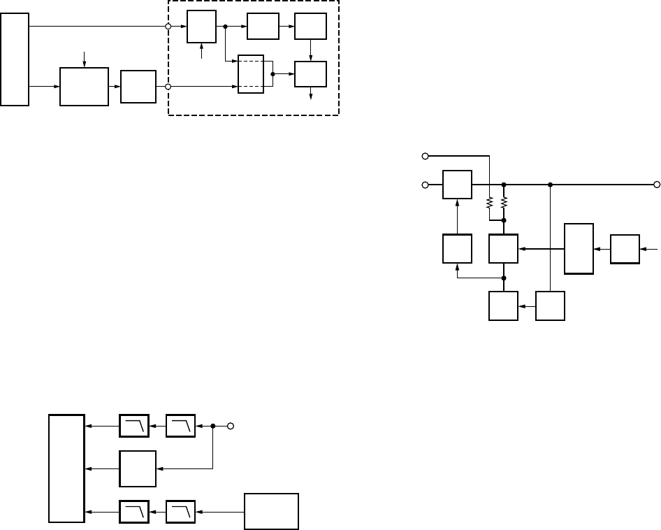
28
TK-760G/762G
■Encode
The QT and DQT signals are output from TO of the CPU
(IC502) and summed with the external pin DI line by the
summing amplifier (IC2) and the resulting signal goes to the
D/A converter (IC6) of the TX-RX unit. The DTMF and 2-
TONE signals are output from DTMF of the CPU and goes to
the audio processor (IC508). The signal is summed with a
MIC signal by the audio processor (IC508), and the resulting
signal passes through an analog switch (IC509) and goes to
the TX-RX unit (MO).
The D/A converter (IC6) adjusts the MO level and the bal-
ance between the MO and TO levels. Part of a TO signal is
summed with MO and the resulting signal goes to the MD
pin of the VCO. This signal is applied to a varicap diode in
the VCO for direct FM modulation.
■D/A Converter
The D/A converter (IC6) is used to adjust TONE and MO
modulation, AF volume, TV voltage, FC reference voltage,
and PC POWER CONTROL voltage level.
Adjustment values are sent from the CPU as serial data.
The D/A converter has a resolution of 256 and the following
relationship is valid:
D/A output = (Vin – VDAref) / 256 x n + VDAref
Vin: Analog input
VDAref: D/A reference voltage
n: Serial data value from the microprocessor (CPU)
Power Supply Circuit
When the POWER switch on the control unit is pressed,
the PSW signal goes low. This signal is inverted by Q26 and
sent to a flip-flop IC (IC14). This IC outputs a control signal
when the PSW goes low. When the power turns on, pin 1
of IC14 outputs a low signal and Q20 turns on. The base of
Q19 goes high, Q19 turns on, SB SW (Q23) turns on and
power (SB) is supplied to the set.
This circuit has an overvoltage protection circuit. If a DC
voltage of 20 V or higher is applied to the power cable, D21
turns on and a voltage is applied to the base of Q21. This
voltage turns Q21 on and turns Q19 and SBSW off.
■Decode
• QT/DQT/DTMF
The signal (DEO) detected by the TX-RX unit passes
through two low-pass filters of IC513, goes to TOI of the
CPU (IC502) to decode QT, DQT. The DTMF signal is de-
coded by a dedicated IC (IC511) and the resulting signal is
sent to the CPU (IC502) as serial data.
• 2-tone
The detected signal passes through audio processor
(IC508) RX OUT. Then it is filtered through IC504 2-stage
low-pass filtered to enter CPU (IC502) to decode 2-tone sig-
nalling.
CIRCUIT DESCRIPTION
Fig. 14 Encode
Fig. 15 Decode
X1
VCXO
IC6
D/A
A1
VCO
IC1
SUM
AMP
IC509
Analog
SW
IC508
Audio
processor
IC3
PLL
MB
MD
MO
TO
HT
DI
MIC
TX-RX UNIT
TO
DTMF
IC502
CPU
IC502
CPU
IC513(2/2)
LPF
IC513(1/2)
LPF
TOI
IC511
DTMF
DECO.
IC508
Audio
processor
STD
DEO
IC514(2/2)
LPF
IC514(1/2)
LPF
2TN
RXOUT
Q23
SW
Q19
SW
Q20
SW
Q26
INV.
IC14
F. F.
Q21
SW
D21
SW
R135
R134
IGN
SB +B
PSW
Fig. 16 Power supply circuit

29
TK-760G/762G
SEMICONDUCTOR DATA
■Terminal function
Pin No. Name I/O Function
1 EMGT O
External MIC control. Mobile MIC : H
2 DTMF O DTMF/2TONE/BEEP output.
3 2TN I 2TONE decode pulse input.
4 DTMSTD I DTMF decode detect. Detect : H
5 SIM I Destination select.
6 BYTE I +5V (5C).
7 CNVSS I GND.
8 AFSTB O Base band IC strobe/reset output.
9 AFFCLK O Base band IC frame detect reset/
system reset output.
10 RESET I Reset.
11 XOUT O Clock output.
12 VSS – GND.
13 XIN I Clock input.
14 VCC – +5V.
15 NC I Pull up.
16 MICDAT I/O MIC data input/output.
17 AUX3 I/O Option board port 3.
SmarTrunk : Clock output.
18 NC – NC.
19 OE I Output enable control sift register.
20 NC – NC.
21 EEPDAT I/O EEPROM data input/output.
22 TO O QT/DQT modulation output.
23 AUX1 I Option board port 1.
SmarTrunk : Req/Ack input.
24 SFTSTB1 O Shift register strobe output.
25 DACSTB O D/A converter enable output.
26 PTT I PTT. PTT on : L
27 NC – NC.
28 NC – NC.
29 AUX4 O Option board port 4.
SmarTrunk : Data output.
30 AUX2 I/O Option board port 2.
SmartTrunk : Data input.
31 PA O MIC audio line sw control. PA : H
32 KOUT2 O Key scan output 2.
33 TXD O Serial data. PTT on : L
34 HOOK I HOOK/RXD. On hook : L
35 KOUT1 O Key scan output 1.
36 KOUT0 O Key scan output 0.
Pin No. Name I/O Function
37 RDY I Pull up.
38 NC – NC.
39 HOLD I Not used.
40,41 NC – NC.
42 RD O READ signal.
43 NC – NC.
44 WR O WRITE signal.
45 LCDCS O LCD chip enable output.
46 CNTDAT O Common data output. (LCD,
SHIFT REG, VOL, Audio processor)
47 CNTCLK O Common clock output. (EEPROM,
LCD, SHIFT REG, VOL, Audio processor)
48 CSO – Chip select signal.
49 A19 – Not used.
50~59 A18~A9 – Flash memory address bus.
60 ACC – +5V.
61 A8 – Flash memory address bus.
62 VSS – GND.
63~70 A7~A0 – Flash memory address bus.
71~73 KIN0~KIN2 I Key scan input.
74 MON I [MON] key input. On : L
75 SCN I [SCN] key input. On : L
76 PLLUL I
PLL unlock detect input. Unlock : L
77 PLLSTB O PLL strobe output. Latch : H
78 MUTE I RX audio mute. Mute : H
79~86 D7~D0 – Flash memory data bus.
87 PWR (EMG) I
[PWR] key input (key interrupt). On : L
88 EMG/TXS I
Emergency input (key interrupt). On : L
89 RFDAT O PLL data output.
90 RFCLK O PLL clock output.
91 NC – NC.
92 RSSQL I
Receive signal strength indicator input.
93 ANLSQL I Analog squelch level input.
94 AVSS – GND.
95 TOI I QT/DQT signal input.
96 VREF – Reference voltage input.
97 AVCC – +5V.
98 DTMPD O DTMF IC power control.
Power down : H
99 DTMCLK O DTMF IC decode clock output.
100 DTMDAT I DTMF IC decode data input.
Microprocessor : 30622M4102GP (TX-RX Unit IC502)
30
TK-760G/762G
SEMICONDUCTOR DATA
Shift Register : BU4094BCFV
■Terminal function (TX-RX unit IC510)
Pin No.
Port Name Function
4 Q1 W/N Wide/Narrow SW. Narrow : H
5 Q2 MUTE
MIC mute (M models only). Mute : H
6 Q3 MBL MIC/LCD backlight control.
Backlight on : H
7 Q4 LED0 Red LED. LED lights : H
11 Q8 BSHIFT Beat shift. Shift on : H
12 Q7 AFREG2 Base band IC inter register select 2.
13 Q6 AFREG1 Base band IC inter register select 1.
14 Q5 LED1 Green LED. LED lights : H
■Terminal function (TX-RX unit IC9)
Pin No.
Port Name Function
4 Q1 HNC
Horn alert control. Horn alert on : H
5 Q2 8RC 8R control. RX : H
6 Q3 8TC 8T control. TX : H
7 Q4 SPMUTE
Speaker mute control. Mute on : H
11 Q8 AUX6
Option board port 6 (AUX6). AUX on : H
12 Q7 AUX5 Option board port 5 (AUX5).
13 Q6 PA/LI
PA/LIGHT control. PA/LIGHT on : H
14 Q5 RX TX/RX VCO switch. RX : L
LCD Driver : LC75833W
(Display Unit IC801 : TK-762G only)
■Block diagram
Common
driver Segment driver & latch
Clock
generator Shift register
Address
detector
COM3
COM2
COM1
S35
S34
S9
S8/P8
S2/P2
S1/P1
INH
OSC
VDD
VLCD
VLCD1
VLCD2
VSS
DI
CL
CE
■Terminal function
Pin No. Name I/O Function
1~8
S1/P1~S8/P8
O Segment output for displaying data
9~35 S9~S35 transferred from serial data.
36~38
COM1~COM3
O Common driver output. Frame
frequency fo=(fosc/384)Hz
39 VDD – Power supply for logic section
(2.7V~6.0V).
40 VLCD – Power supply for LCD driver section
(2.7V~6.0V).
41 VLCD1 I Apply 2/3 the LCD drive bias voltage
from outside. If 1/2 the bias is
applied, connect to VLCD2.
42 VCLD2 I Apply 1/3 the LCD drive bias voltage
from outside. If 1/2 the bias is
applied, connect to VLCD1.
43 VSS – GND.
44 OSC I/O Oscillation terminal.
45 INH I
Force the display to turn off regardless
of internal data. Serial data can be input
regardless of whether it is "H" or "L".
46 CE I Chip enable. Serial data transfer
terminal. Connected to the
microprocessor.
47 CL I Synchronizing clock. Serial data
transfer terminal. Connected to
the microprocessor.
48 DI I Transfer data. Serial data transfer
terminal. Connected to the
microprocessor.
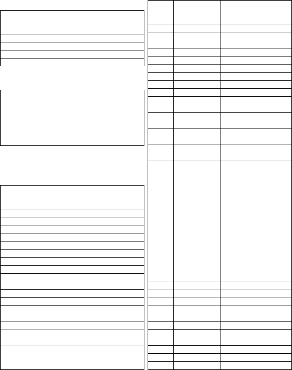
31
TK-760G/762G
DESCRIPTION OF COMPONENTS
Display Unit (X54-3270-10) : TK-760G
Ref. No. Use/Function Operation/Condition
D801 Reverse current
prevention
D802~805
Light emission
D808 Current stability
IC801 LCD driver
Q801 DC switch (LED)
Display Unit (X54-3280-10) : TK-762G
Ref. No. Use/Function Operation/Condition
D801 Light emission
D802 Reverse current
prevention
D803,804
Light emission
IC801 LCD driver
Q801~809
DC switch (LED)
TX-RX Unit (X57-5950-XX)
-10 : TK-760G K -11 : TK-762G K -12 : TK-760G K2
-13 : TK-762G K2 -21 : TK-760G M
Ref. No. Use/Function Operation/Condition
D1 Surge absorption
D2 Voltage reference
D3~5 Surge absorption
D8
IF switch (Wide/narrow)
D9 DC switch
D10
IF switch (Wide/narrow)
D11 Noise amp detect
D14 Surge absorption
D15 OR gate SP mute, AM
D16 RF switch (TX/RX) Heterodyne
D17 Temperature Drive
compensation
D18 RF BPF tuning
D19 Surge absorption
D20 Reverse current
prevention
D21 Voltage reference
D22 Temperature Drive
compensation
D23 RF BPF tuning
D24 Voltage reference
D25 Surge absorption
Ref. No. Use/Function Operation/Condition
D27 Reverse current
prevention
D28 RF BPF tuning
D29 Reverse current
prevention
D30,31 RF BPF tuning
D33,34 ANT switch
D35,36
APC voltage detect
D39 Voltage reference Power protection
D40 Charge DEO
D41 Voltage drop Charge pump
D501 Reverse current KOUT 0
prevention
D502 Reverse current KOUT 1
prevention
D503 Reverse current KOUT 2
prevention
D504 Reverse current KOUT 0
prevention
D505 Reverse current KOUT 1
prevention
D506 Voltage discharger When powering down
D507 Reverse current KOUT 2
prevention
D508 Limiter MIC
D509~514
Key backlight Active while MBL is H
D521 Busy/TX LED Lights green while busy,
red while TX
D523 OR gate MIC mute, MM, MM2
D524 Surge absorption HOOK/RXD
D525 Surge absorption PTT/TXD
D526 Current protection
D527 Surge absorption CM
D528 Surge absorption MBL
D529 Limiter QT/DQT decode limiter
IC1 Sum amplifier DI, TO mixer
IC2 DC amplifier FC, TCXO control
IC3 PLL synthesizer Reference 16.8MHz,
PLL lock : LD H
IC4 Amplifier DEO
IC5 FM demodulation Quadrature detector, 2nd mixer,
OSC, IF amplifier, RSSI
IC6 D/A converter
IC7 DC amplifier PC/TV control
IC8 Prescaler 1/2 prescaler

32
TK-760G/762G
DESCRIPTION OF COMPONENTS
Ref. No. Use/Function Operation/Condition
IC9 Shift/Store register HNC, 8RC, 8TC, SPMUTE, RX,
PA/LI, AUX5, AUX6
IC10 5V AVR 5C (TX/RX)
IC11 9V AVR 9C
IC12 8V AVR 8C
IC13 AF amplifier
IC14 Power supply logic
circuit control
IC15 DC amplifier APC control
IC400 Power module
IC501 Flash ROM
IC502 CPU
IC503 Reset IC Low voltage output when
powering up
IC505 EEPROM
IC507 Amplifier MIC, AFO
IC508 Audio processor Compander, MIC amplifier,
ALC, AF filter, IDC
IC509 Analog switch MO, DEO, EMG, MI switch
IC510 Shift/Store register W/N, MM2, MBL, LED0, LED1,
AFREG1, AFREG2, BSHIFT
IC511 DTMF decode
IC512 5V AVR 5C (control)
IC513 Amplifier QT/DQT decode
IC514 Amplifier 2-Tone decode
Q1 DC switch HOR
Q2 DC switch 5S
Q3 DC switch (W/N) Active while it is narrow
Q4 DC switch (W/N) Active while it is wide
Q5 DC switch HNC
Q6 DC switch IGN
Q7 Buffer amplifier 16.8MHz x 3
Q8 Lipple filter 8CL
Q9 Buffer amplifier PLL fin
Q10 Noise amplifier Squelch
Q11 Charge pump øP
Q12 Charge pump øR
Q13 IF amplifier 49.95MHz
Q14 Buffer amplifier Hetetodyne
Q15 Mixer
Q16 DC switch 8R cont, active while RX
Q17 AF mute Active while AF mute
Q18 DC switch 8R, active while RX
Q19,20 DC switch SB switch, active when
powering up
Ref. No. Use/Function Operation/Condition
Q21 DC switch Active while PS voltage is more
than 20V
Q22 RF amplifier Predrive
Q23 DC switch SB switch, active when
powering up
Q24 AF mute
Active while power switch is off
Q25 RF amplifier Drive
Q26 Inverter
Active while power switch is low
Q27 L.N.A.
Q28 DC switch 8T, active while TX
Q29 DC switch 8T cont, active while TX
Q31 APC controller
Q32 APC controller DB
Q33 APC controller Power protection
Q35 W/N switch Active on narrow
Q36 DC switch Power protection
Q37 AF mute switch Inactive on mute
Q38 DC switch 5S
Q39 DC switch Output enable
Q501 Clock switch shift
Clock shift is on while BSHIFT is H
Q502 AF mute Active while MUTE is H
Q503 Inverter Active while PA2 is H,
active while public address
Q504 LED switch (Red) Active while LED0 is H,
active while TX
Q505,506 Key backlight switch Active while MBL is H
Q508 LED switch (Green) Active while LED1 is H,
active while RX
Q509 MIC mute Active while MM is H and
MM2 is H
PLL/VCO (X58-4670-XX) -10 : K,M -11 : K2
Ref. No. Use/Function Operation/Condition
D101 RX VCO
D102 TX VCO
D103 RX VCO
D104 TX VCO
D105 Modulation
Q101 Oscillator RX
Q102 Inverter Active while ST is H
Q103 Oscillator TX
Q104 TX/RX switch (TX) Active while ST is H
Q105 TX/RX switch (RX) Active while Q102 is off
Q106 Buffer amplifier
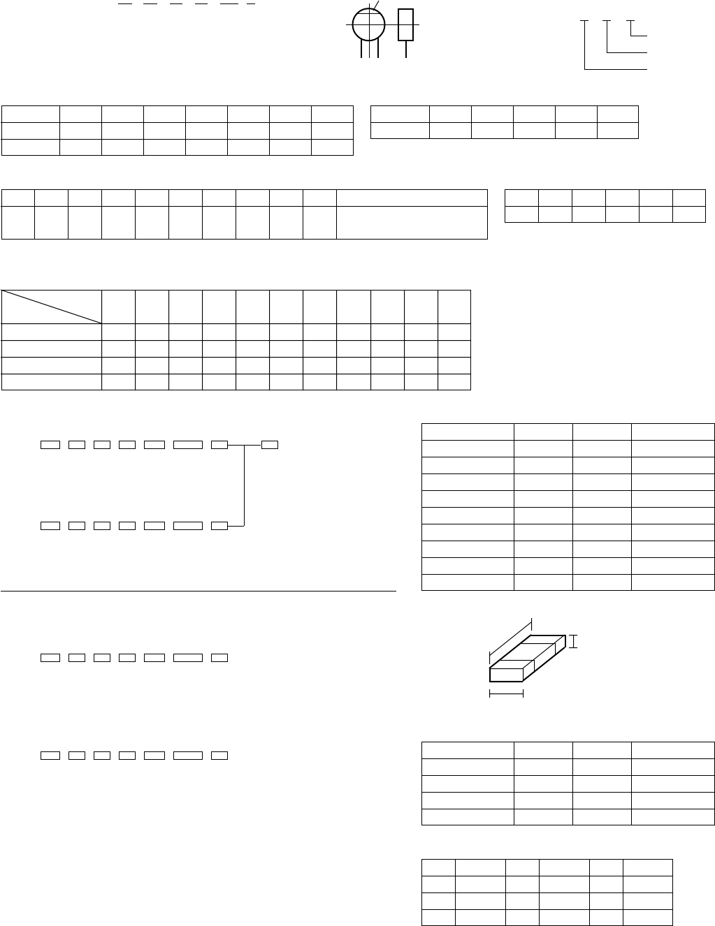
33
TK-760G/762G
2nd Word G H J K L
ppm/°C±30 ±60 ±120 ±250 ±500
Example : CC45TH = –470 ± 60ppm/°C
Multiplier
2nd number
1st number
2 2 0 = 22pF
CAPACITORS CC 45 TH 1H 220 J
12 3 4 56
1 = Type … ceramic, electrolytic, etc. 4 = Voltage rating
2 = Shape … round, square, ect. 5 = Value
3 = Temp. coefficient 6 = Tolerance
• Temperature coefficient
1st Word C L P R S T U
Color* Black Red Orange Yellow Green Blue Violet
ppm/°C 0 –80 –150 –220 –330 –470 –750
• Tolerance (More than 10pF)
Code C D G J K M X Z P No code
(%) ±0.25 ±0.5 ±2±5±10 ±20 +40 +80 +100 More than 10µF – 10 ~ +50
–20 –20 –0 Less than 4.7µF –10 ~ +75
• Voltage rating
ABCDEFGHJKV
0 1.0 1.25 1.6 2.0 2.5 3.15 4.0 5.0 6.3 8.0 –
1 10 12.5 16 20 25 31.5 40 50 63 80 35
2 100 125 160 200 250 315 400 500 630 800 –
3 1000 1250 1600 2000 2500 3150 4000 5000 6300 8000 –
• Chip capacitors
(EX) C C 7 3 F S L 1 H 0 0 0 J
12345 6 7
(Chip) (CH, RH, UJ, SL)
(EX) C K 7 3 F F 1 H 0 0 0 Z
12345 6 7
(Chip) (B, F)
RESISTORS
• Chip resistor (Carbon)
(EX) R D 7 3 E B 2 B 0 0 0 J
12345 6 7
(Chip) (B,F)
• Carbon resistor (Normal type)
(EX) R D 1 4 B B 2 C 0 0 0 J
12345 6 7
1 = Type … ceramic, electrolytic, etc. 5 = Voltage rating
2 = Shape … round, square, ect. 6 = Value
3 = Dimension 7 = Tolerance
4 = Temp. coefficient
• Capacitor value
010 = 1pF
100 = 10pF
101 = 100pF
102 = 1000pF = 0.001µF
103 = 0.01µF
(Less than 10pF)
Code B C D F G
(pF) ±0.1 ±0.25 ±0.5 ±1±2
1st word
2nd word
Refer to the table above.
Dimension (Chip capacitors)
Dimension code L W T
Empty 5.6 ± 0.5 5.0 ± 0.5 Less than 2.0
A 4.5 ± 0.5 3.2 ± 0.4 Less than 2.0
B 4.5 ± 0.5 2.0 ± 0.3 Less than 2.0
C 4.5 ± 0.5 1.25 ± 0.2 Less than 1.25
D 3.2 ± 0.4 2.5 ± 0.3 Less than 1.5
E 3.2 ± 0.2 1.6 ± 0.2 Less than 1.25
F 2.0 ± 0.3 1.25 ± 0.2 Less than 1.25
G 1.6 ± 0.2 0.8 ± 0.2 Less than 1.0
H 1.0 ± 0.05 0.5 ± 0.05 0.5 ± 0.05
Dimension
Dimension (Chip resistor)
Dimension code L W T
E 3.2 ± 0.2 1.6 ± 0.2 1.0
F 2.0 ± 0.3 1.25 ± 0.2 1.0
G 1.6 ± 0.2 0.8 ± 0.2 0.5 ± 0.1
H 1.0 ± 0.05 0.5 ± 0.05 0.35 ± 0.05
Rating wattage
Code Wattage Code Wattage Code Wattage
1J 1/16W 2C 1/6W 3A 1W
2A 1/10W 2E 1/4W 3D 2W
2B 1/8W 2H 1/2W
1 = Type
2 = Shape
3 = Dimension
4 = Temp. coefficient
5 = Voltage rating
6 = Value
7 = Tolerance
CC45 Color*
T
W
L
PARTS LIST

TK-760G/762G
PARTS LIST
34
*New Parts. indicates safety critical components.
Parts without Parts No. are not supplied.
Les articles non mentionnes dans le Parts No. ne sont pas fournis.
Teile ohne Parts No. werden nicht geliefert.
L: Scandinavia K: USA P: Canada
Y: PX (Far East, Hawaii) T: England E: Europe
Y: AAFES (Europe) X: Australia M: Other Areas
TK-760G/762G
DISPLAY UNIT (X54-3270-10) : TK-760G, DISPLAY UNIT (X54-3280-10) : TK-762G
New
Desti-
parts
nation
Ref. No.
Address
Parts No. Description
New
Desti-
parts
nation
Ref. No.
Address
Parts No. Description
1 1B,1E A01-2165-13 CABINET UPPER
2 2A,2D A01-2166-13 CABINET LOWER
3 2A A62-0642-03 PANEL ASSY 760
3 2D A62-0731-03 PANEL ASSY 762
5 1G B09-0235-05 CAP
6 2B B11-1226-03 ILLUMINATION GUIDE 760
6 2E B11-1230-03 ILLUMINATION GUIDE 762
7 2A B38-0824-05 LCD 760
7 2E B38-0825-05 LCD 762
8 2G * B62-1257-10 INSTRUCTION MANUAL M
8 2G B62-1258-00 INSTRUCTION MANUAL K,K2
9 1C B72-1690-04 MODEL NAME PLATE 760K
9 1C B72-1691-04 MODEL NAME PLATE 760M
9 1F B72-1694-04 MODEL NAME PLATE 762K
9 1C B72-1742-04 MODEL NAME PLATE 760K2
9 1F B72-1744-04 MODEL NAME PLATE 762K2
11 2B E29-1179-04 INTER CONNECTOR 760
11 2E E29-1183-04 INTER CONNECTOR 762
12 1C E30-2145-15 ANTENNA CABLE
13 1G E30-3339-05 DC CORD ACC
14 1C,1F E30-3340-05 DC CORD RADIO
- - E30-3404-05 TRUNK CABLE
16 1C,1F E37-0790-15 LEAD WIRE WITH CONNECTOR (SP)
17 2B,2E E37-0815-05 FLAT CABLE
19 1G F51-0016-05 FUSE (6*30) 10A
21 1C,1F G02-0791-04 FLAT SPRING AF,APC
22 1B,1E G10-1221-04 FIBROUS SHEET SIDE
23 1B,1E G10-1222-14 FIBROUS SHEET UP,DOWN
24 1A,1D G10-1223-14 FIBROUS SHEET SHIELD
25 1C,1F G13-1468-04 CUSHION DC CORD
26 1B,1E G13-1759-04 CUSHION SP
27 2C,2F G53-0796-04 PACKING PHONE JACK
28 2E G53-0889-04 PACKING DISPLAY UNIT 762
30 3G H10-6618-12 POLYSTYRENE FOAMED FIXTURE (F)
31 2H H10-6619-12 POLYSTYRENE FOAMED FIXTURE (R)
32 1G H12-1391-03 INNER PACKING CASE
33 1H,2H H25-0720-04 PROTECTION BAG (200X350)
34 3H H52-1519-02 ITEM CARTON CASE
36 2G J19-1584-05 HOLDER ACC
37 2A,2D J21-8382-03 HARDWARE FIXTURE
38 1G J29-0627-23 BRACKET
40 2A K29-5343-02 KEY TOP 760
40 2D K29-5344-02 KEY TOP 762
A 2A,2D N33-2606-45 OVAL HEAD MACHINE SCREW
B 2C,2F N67-3008-46 PAN HEAD SEMS SCREW W
C 2B,2E N87-2606-46 BRAZIER HEAD TAPTITE SCREW
D 2B,2E N87-2612-46 BRAZIER HEAD TAPTITE SCREW
42 2G N99-0395-05 SCREW SET
44 1B,1E T07-0368-05 SPEAKER
45 1G T91-0597-15 MICROPHONE K,K2
TK-760G/762G
D802-805 * B30-2220-05 LED (2P/YELLOW)
C801-803 CC73GCH1H101J CHIP C 100PF J
C804 CK73GF1A105Z CHIP C 1.0UF Z
C805 CK73GB1H102K CHIP C 1000PF K
C806,807 CK73GB1H471K CHIP C 470PF K
CN801 E40-6020-05 PIN ASSY
L801 L92-0138-05 FERRITE CHIP
R801-803 RK73GB1J103J CHIP R 10K J 1/16W
R804 RK73GB1J473J CHIP R 47K J 1/16W
R805 RK73GB1J474J CHIP R 470K J 1/16W
R806 R92-1252-05 CHIP R 0 OHM
R808 RK73GB1J392J CHIP R 3.9K J 1/16W
R809 RK73FB2A270J CHIP R 27 J 1/10W
D801 MA2S111 DIODE
D808 HSB123 DIODE
IC801 LC75823W IC (MOS-IC)
Q801 2SB1132(Q,R) TRANSISTOR
D801 B30-2204-05 LED (RED/YELLOW)
D803 B30-2220-05 LED (2P/YELLOW)
D804 B30-2204-05 LED (RED/YELLOW)
C801 CK73GB1H471K CHIP C 470PF K
C802-804 CC73GCH1H101J CHIP C 100PF J
C805 CK73GF1A105Z CHIP C 1.0UF Z
C806 CK73GB1H471K CHIP C 470PF K
C807 CK73GB1H102K CHIP C 1000PF K
C808 CK73GB1H471K CHIP C 470PF K
C812 CK73GB1H471K CHIP C 470PF K
CN801 E40-6020-05 PIN ASSY
L801 L92-0138-05 FERRITE CHIP
R801,802 RK73GB1J103J CHIP R 10K J 1/16W
R803 RK73FB2A123J CHIP R 12K J 1/10W
R804 RK73GB1J103J CHIP R 10K J 1/16W
R805 RK73FB2A332J CHIP R 3.3K J 1/10W
R806 RK73GB1J474J CHIP R 470K J 1/16W
R807 R92-1252-05 CHIP R 0 OHM
R808 RK73GB1J393J CHIP R 39K J 1/16W
R809 RK73FB2A123J CHIP R 12K J 1/10W
R810 RK73FB2A332J CHIP R 3.3K J 1/10W
R812 RK73FB2A561J CHIP R 560 J 1/10W
R813-816 RK73GB1J473J CHIP R 47K J 1/16W
D802 MA2S111 DIODE
IC801 LC75833W IC (LCD DRIVER)
Q801-803 DTA114EKA DIGITAL TRANSISTOR
Q804 KRA225S TRANSISTOR
Q805 DTA114EKA DIGITAL TRANSISTOR
Q806-809 2SK1824 FET
DISPLAY UNIT (X54-3270-10) : TK-760G
DISPLAY UNIT (X54-3280-10) : TK-762G

TK-760G/762G
PARTS LIST
35
Ref. No.
Address
Parts No. Description Ref. No.
Address
Parts No. Description
New
Desti-
parts
nation
New
Desti-
parts
nation
D509-514 B30-2050-05 LED
D521 B30-2151-05 LED (RED/GRN)
C1-19 CK73GB1H102K CHIP C 1000PF K
C20 C92-0507-05 CHIP-TAN 4.7UF 6.3WV
C21 CK73GB1H102K CHIP C 1000PF K
C22 CK73GB1C104K CHIP C 0.10UF K
C23,24 C92-0507-05 CHIP-TAN 4.7UF 6.3WV
C26 CK73GB1H102K CHIP C 1000PF K
C29 C92-0507-05 CHIP-TAN 4.7UF 6.3WV
C30 CC73GCH1H050C CHIP C 5.0PF C
C31 CK73GB1H102K CHIP C 1000PF K
C32 C92-0662-05 CHIP-TAN 15UF 6.3WV
C33 CC73GCH1H220J CHIP C 22PF J
C35 CK73GB1C104K CHIP C 0.10UF K
C36 CK73GB1H102K CHIP C 1000PF K
C37 CK73FB1C334K CHIP C 0.33UF K
C40,41 CK73GB1H103K CHIP C 0.010UF K
C43 C92-0507-05 CHIP-TAN 4.7UF 6.3WV
C44 CK73GB1H331K CHIP C 330PF K
C45 CK73GB1H102K CHIP C 1000PF K
C46 CK73GB1H103K CHIP C 0.010UF K
C47 C92-0561-05 CHIP-ELE 22UF 16WV
C49 CK73GB1H102K CHIP C 1000PF K
C50 CC73GCH1H220J CHIP C 22PF J
C51 CK73GB1C104K CHIP C 0.10UF K
C52 CC73GCH1H680J CHIP C 68PF J
C53 CK73GB1C104K CHIP C 0.10UF K
C54 CK73GB1H103K CHIP C 0.010UF K
C56 CC73GCH1H220J CHIP C 22PF J
C58 CK73GB1E223K CHIP C 0.022UF K
C60,61 CK73GB1H102K CHIP C 1000PF K
C62 CC73GCH1H101J CHIP C 100PF J
C63 CK73GB1C104K CHIP C 0.10UF K
C64 CK73GB1H103K CHIP C 0.010UF K
C66,67 CK73GB1H102K CHIP C 1000PF K
C69 CK73GB1E223K CHIP C 0.022UF K
C70 C92-0507-05 CHIP-TAN 4.7UF 6.3WV
C72 C92-0507-05 CHIP-TAN 4.7UF 6.3WV
C74,75 CK73GB1H102K CHIP C 1000PF K
C77 C90-2046-05 ELECTRO 22UF 10WV
C78 CK73GB1H102K CHIP C 1000PF K
C79,80 CK73GB1H221K CHIP C 220PF K
C81 CK73GB1H102K CHIP C 1000PF K
C82 C92-0507-05 CHIP-TAN 4.7UF 6.3WV
C83 CC73GCH1H270J CHIP C 27PF J
C84 C92-0507-05 CHIP-TAN 4.7UF 6.3WV
C86 C92-0662-05 CHIP-TAN 15UF 6.3WV
C87 CC73GCH1H330J CHIP C 33PF J
C88 CK73GB1H103K CHIP C 0.010UF K
C91 CC73GCH1H050C CHIP C 5.0PF C
C92 CK73GB1H102K CHIP C 1000PF K
C93 C92-0555-05 CHIP-TAN 0.047UF 35WV
C94 CK73GB1H102K CHIP C 1000PF K
C95 CC73GCH1H020B CHIP C 2.0PF B
C96 CK73GB1H102K CHIP C 1000PF K
C97 C92-0546-05 CHIP-TAN 68UF 6.3WV
C98 CK73GB1H103K CHIP C 0.010UF K
C99 C92-0004-05 CHIP-TAN 1.0UF 16WV
C100 CK73GB1H102K CHIP C 1000PF K
C101 CC73GCH1H040C CHIP C 4.0PF C
C102,103 CK73GB1H102K CHIP C 1000PF K
C104 C92-0002-05 CHIP-TAN 0.22UF 35WV
C105 CK73GB1H102K CHIP C 1000PF K
C106 CC73GCH1H180J CHIP C 18PF J
C107 CK73GB1H102K CHIP C 1000PF K
C110 CC73GCH1H180J CHIP C 18PF J
C111 CC73GCH1H040C CHIP C 4.0PF C
C112 CK73GB1H102K CHIP C 1000PF K
C113 C92-0507-05 CHIP-TAN 4.7UF 6.3WV
C114 C92-0697-05 CHIP-TAN 3.3UF 16WV
C115 CK73GB1H102K CHIP C 1000PF K
C116 CK73GB1H103K CHIP C 0.010UF K
C117 CK73GB1H102K CHIP C 1000PF K
C118 CC73GCH1H100D CHIP C 10PF D
C119 CK73GB1H103K CHIP C 0.010UF K
C120 CC73GCH1H220J CHIP C 22PF J K,M
C120 CC73GCH1H330J CHIP C 33PF J K2
C121 CK73GB1H102K CHIP C 1000PF K
C122,123 CK73GB1C104K CHIP C 0.10UF K
C124 CC73GCH1H101J CHIP C 100PF J
C125 C92-0004-05 CHIP-TAN 1.0UF 16WV
C126 CC73GCH1H180J CHIP C 18PF J
C127 CK73GB1H103K CHIP C 0.010UF K
C128 C92-0543-05 CHIP-TAN 3.3UF 10WV
C129 CK73FF1C105Z CHIP C 1.0UF Z
C130 CK73GB1H103K CHIP C 0.010UF K
C131-133 CK73GB1H102K CHIP C 1000PF K
C134 CK73FB1E104K CHIP C 0.10UF K
C135 CC73GCH1H090D CHIP C 9.0PF D K,M
C135 CC73GCH1H120J CHIP C 12PF J K2
C136 CK73GB1C104K CHIP C 0.10UF K
C137 CC73GCH1H101J CHIP C 100PF J
C138 CK73FB1E104K CHIP C 0.10UF K
C139 CK73GB1H102K CHIP C 1000PF K
C141 C92-0719-05 ELECTRO 47UF 25WV
C142-144 CK73GB1H102K CHIP C 1000PF K
C146-149 CK73GB1H102K CHIP C 1000PF K
C150 CK73FF1C105Z CHIP C 1.0UF Z
C151 CK73GB1H102K CHIP C 1000PF K
C152 CC73GCH1H030C CHIP C 3.0PF C K,M
C152 CC73GCH1H050C CHIP C 5.0PF C K2
C153 CC73GCH1H330J CHIP C 33PF J
C154 CK73GB1H102K CHIP C 1000PF K
C155 CC73GCH1H220J CHIP C 22PF J
C156,157 CK73GB1H102K CHIP C 1000PF K
C158 CC73GCH1H390J CHIP C 39PF J
C159 CC73GCH1H180J CHIP C 18PF J
C160,161 C92-0719-05 ELECTRO 47UF 25WV
C162 CK73GB1H102K CHIP C 1000PF K
C163 CC73GCH1H010B CHIP C 1.0PF B
C164 CK73GB1H102K CHIP C 1000PF K
C165 C92-0719-05 ELECTRO 47UF 25WV
C166 CE04EW1E471M ELECTRO 470UF 25WV
C167 CC73GCH1H150J CHIP C 15PF J
C168-170 CK73GB1H102K CHIP C 1000PF K
C171 CC73GCH1H020B CHIP C 2.0PF B
TX-RX UNIT (X57-5950-XX)
TX-RX UNIT (X57-5950-XX)
-10 : TK-760G K -11 : TK-762G K -12 : TK-760G K2
-13 : TK-762G K2 -21 : TK-760G M

TK-760G/762G
PARTS LIST
36
Ref. No.
Address
Parts No. Description Ref. No.
Address
Parts No. Description
New
Desti-
parts
nation
New
Desti-
parts
nation
C172 CE04EW1E471M ELECTRO 470UF 25WV
C173 CK73GB1C104K CHIP C 0.10UF K
C174 CK73GB1H102K CHIP C 1000PF K
C175 CC73GCH1H080D CHIP C 8.0PF D K,M
C175 CC73GCH1H100D CHIP C 10PF D K2
C177 CK73GB1H102K CHIP C 1000PF K
C179 CK73GB1H102K CHIP C 1000PF K
C180 CK73GB1H103K CHIP C 0.010UF K
C181 CC73FCH1H120J CHIP C 12PF J
C183 CK73GB1H102K CHIP C 1000PF K
C185 CK73GB1C104K CHIP C 0.10UF K
C186,187 CK73GB1H102K CHIP C 1000PF K
C189,190 CK73GB1H102K CHIP C 1000PF K
C192 CK73GB1H102K CHIP C 1000PF K
C194 CK73GB1C104K CHIP C 0.10UF K
C195 C92-0719-05 ELECTRO 47UF 25WV
C196 CK73GB1H102K CHIP C 1000PF K
C198 CK73GB1H102K CHIP C 1000PF K
C200 CK73GB1H102K CHIP C 1000PF K
C201 CK73GB1C104K CHIP C 0.10UF K
C203 CK73GB1H102K CHIP C 1000PF K
C204 C92-0004-05 CHIP-TAN 1.0UF 16WV
C205 C93-0558-05 CHIP C 8.0PF D K2
C205 C93-0560-05 CHIP C 10PF D K,M
C207 CK73GB1H103K CHIP C 0.010UF K
C208 CC73FCH1H030C CHIP C 3.0PF C K,M
C208 CC73FCH1H040C CHIP C 4.0PF C K2
C209 C93-0563-05 CHIP C 18PF J K2
C209 C93-0564-05 CHIP C 22PF J K,M
C210 CK73GB1H103K CHIP C 0.010UF K
C211 C93-0564-05 CHIP C 22PF J
C212 CK73GB1H102K CHIP C 1000PF K
C213 C93-0563-05 CHIP C 18PF J
C214 C93-0603-05 CHIP C 1000PF K
C215 C93-0561-05 CHIP C 12PF J
C216 CC73GCH1H0R5B CHIP C 0.5PF B
C217 CC73GCH1H010B CHIP C 1.0PF B
C218 CK73GB1C104K CHIP C 0.10UF K K,M
C219 C93-0565-05 CHIP C 27PF J
C220 CK73GB1H102K CHIP C 1000PF K
C221 C93-0563-05 CHIP C 18PF J K,M
C221 C93-0565-05 CHIP C 27PF J K2
C222 CC73GCH1H0R5B CHIP C 0.5PF B
C223 CC73GCH1H010B CHIP C 1.0PF B K,M
C223 CC73GCH1H020B CHIP C 2.0PF B K2
C224 CK73GB1H102K CHIP C 1000PF K
C230,231 CK73GB1C104K CHIP C 0.10UF K
C241 C93-0554-05 CHIP C 4.0PF C K,M
C241 C93-0555-05 CHIP C 5.0PF C K2
C248 C92-0585-05 CHIP-TAN 4.7UF 16WV
C259 CK73GB1C104K CHIP C 0.10UF K
C260 CK73GB1H103K CHIP C 0.010UF K
C261 CK73FF1C105Z CHIP C 1.0UF Z
C270 CK73GB1C104K CHIP C 0.10UF K
C271 CK73GB1H472K CHIP C 4700PF K
C272 CS15E1C010M TANTAL 1.0UF 16WV
C274 CK73GB1C104K CHIP C 0.10UF K
C275 C92-0004-05 CHIP-TAN 1.0UF 16WV K2
C501 CK73GB1H102K CHIP C 1000PF K
C502 CK73GB1C104K CHIP C 0.10UF K
C503 CK73GB1H471K CHIP C 470PF K
C504 CK73GB1H103K CHIP C 0.010UF K
C505 CK73GB1C104K CHIP C 0.10UF K
C506,507 CK73GB1H103K CHIP C 0.010UF K
C508 CK73GB1H472K CHIP C 4700PF K
C509 C92-0507-05 CHIP-TAN 4.7UF 6.3WV
C514 CC73GCH1H680J CHIP C 68PF J
C515 CK73GB1H103K CHIP C 0.010UF K
C516 CC73GCH1H270J CHIP C 27PF J
C517 CK73GB1C683K CHIP C 0.068UF K
C518 CC73GCH1H270J CHIP C 27PF J
C519 CK73GB1H102K CHIP C 1000PF K
C520 CK73GB1C104K CHIP C 0.10UF K
C521 CK73GB1H102K CHIP C 1000PF K
C522 C92-0507-05 CHIP-TAN 4.7UF 6.3WV
C523 CC73GCH1H221J CHIP C 220PF J
C524 CK73GB1H103K CHIP C 0.010UF K
C525 CK73GB1E123K CHIP C 0.012UF K
C526 CK73GB1C683K CHIP C 0.068UF K
C527 CK73GB1H222K CHIP C 2200PF K
C528 CK73GB1H103K CHIP C 0.010UF K
C529 CK73GB1H272K CHIP C 2700PF K
C530 CK73GB1H152K CHIP C 1500PF K
C531 CK73GB1H272K CHIP C 2700PF K
C532,533 CK73GB1C104K CHIP C 0.10UF K
C534,535 CK73GB1H103K CHIP C 0.010UF K
C536,537 CK73GB1C104K CHIP C 0.10UF K
C538 C92-0566-05 CHIP-TAN 10UF 6.3WV
C539 CK73GB1H103K CHIP C 0.010UF K
C540,541 CK73GB1C104K CHIP C 0.10UF K
C542 CC73GCH1H331J CHIP C 330PF J
C543 CK73GB1H102K CHIP C 1000PF K
C544-546 CK73GB1H562K CHIP C 5600PF K
C547 CC73GCH1H030C CHIP C 3.0PF C
C548-550 CK73GB1H272K CHIP C 2700PF K
C551 CC73GCH1H151J CHIP C 150PF J
C552 CC73GCH1H030C CHIP C 3.0PF C
C553 CK73GB1H102K CHIP C 1000PF K
C554 CK73GB1H122K CHIP C 1200PF K
C555 C92-0566-05 CHIP-TAN 10UF 6.3WV
C556 CK73GB1C333K CHIP C 0.033UF K
C557 CK73GB1C104K CHIP C 0.10UF K
C558 CC73GCH1H101J CHIP C 100PF J
C559 CK73GB1H102K CHIP C 1000PF K
C560-563 CK73GB1C104K CHIP C 0.10UF K
C564 C92-0507-05 CHIP-TAN 4.7UF 6.3WV
C565,566 CK73GB1H472K CHIP C 4700PF K
C567 CC73GCH1H101J CHIP C 100PF J
C568 C92-0507-05 CHIP-TAN 4.7UF 6.3WV
C569 CK73GB1E223K CHIP C 0.022UF K
C570 CK73FF1C105Z CHIP C 1.0UF Z
C571,572 CK73GB1H102K CHIP C 1000PF K
C573 CK73FB1H563K CHIP C 0.056UF K
C574 CC73GCH1H470J CHIP C 47PF J
C575 CK73GB1H102K CHIP C 1000PF K
C576 CK73GB1C104K CHIP C 0.10UF K
C577,578 CK73GB1H103K CHIP C 0.010UF K
C579 CC73GCH1H101J CHIP C 100PF J
C580 CK73GB1C104K CHIP C 0.10UF K
C581 CK73GB1H102K CHIP C 1000PF K
TX-RX UNIT (X57-5950-XX)

TK-760G/762G
PARTS LIST
37
Ref. No.
Address
Parts No. Description Ref. No.
Address
Parts No. Description
New
Desti-
parts
nation
New
Desti-
parts
nation
C582 CK73GB1C473K CHIP C 0.047UF K
C583 C92-0566-05 CHIP-TAN 10UF 6.3WV
C584 CK73GB1H103K CHIP C 0.010UF K
C585 CC73GCH1H101J CHIP C 100PF J
C587 CK73GB1H103K CHIP C 0.010UF K
C589 C92-0606-05 CHIP-TAN 4.7UF 10WV
C590 CK73GB1H102K CHIP C 1000PF K
C594 CK73GB1H102K CHIP C 1000PF K
C596 CK73GB1H102K CHIP C 1000PF K
C597 CC73GCH1H101J CHIP C 100PF J
C598 CK73GB1H102K CHIP C 1000PF K
C599 CC73GCH1H101J CHIP C 100PF J
C600 CK73GB1H102K CHIP C 1000PF K
C601,602 CC73GCH1H101J CHIP C 100PF J
C603 CK73GB1H102K CHIP C 1000PF K
C604-606 CC73GCH1H101J CHIP C 100PF J
C608-610 CC73GCH1H101J CHIP C 100PF J
C611,612 CK73GB1H471K CHIP C 470PF K
C613 CC73GCH1H101J CHIP C 100PF J
C615 CK73GB1H471K CHIP C 470PF K
C616 CC73GCH1H101J CHIP C 100PF J
C618 CK73GB1H102K CHIP C 1000PF K
C620 CK73GB1H471K CHIP C 470PF K
C621 CK73GB1H102K CHIP C 1000PF K
C623 CK73GB1H102K CHIP C 1000PF K
C626 CK73GB1C104K CHIP C 0.10UF K
C628 CK73GB1C104K CHIP C 0.10UF K
C629 CC73GCH1H470J CHIP C 47PF J
C630 C92-0507-05 CHIP-TAN 4.7UF 6.3WV
C631 CK73GB1H103K CHIP C 0.010UF K
C632 CK73GB0J105K CHIP C 1.0UF K
C633 CK73GB1C104K CHIP C 0.10UF K
C720 C92-0566-05 CHIP-TAN 10UF 6.3WV
CN1 E40-6047-05 PIN ASSY
CN2 E40-6021-05 FLAT CABLE CONNECTOR
CN3 E40-3247-05 PIN ASSY
CN4 E40-5737-05 PIN ASSY
CN5 E40-5738-05 PIN ASSY
CN7 E40-3247-05 PIN ASSY
CN8 E40-3246-05 PIN ASSY
CN501 E40-6021-05 FLAT CABLE CONNECTOR
J1 E11-0442-05 3.5D PHONE JACK (3P)
J501 E08-0877-05 MODULAR JACK
W1 * E37-0856-05 PROCESSED LEAD WIRE
F1 F53-0108-05 FUSE
- J31-0543-05 COLLAR (LH-5-1.5)
CF1 L72-0959-05 CERAMIC FILTER
CF2 L72-0973-05 CERAMIC FILTER
L1 L40-1005-34 SMALL FIXED INDUCTOR (10UH/8)
L2-4 L40-3381-86 SMALL FIXED INDUCTOR (0.33U/160)
L5 L34-4530-05 COIL
L6 L40-1581-86 SMALL FIXED INDUCTOR (0.15U/160)
L7 L40-4785-85 SMALL FIXED INDUCTOR (0.47U/252)
L8 L40-8285-85 SMALL FIXED INDUCTOR (0.82U/252)
L9 L40-1085-77 SMALL FIXED INDUCTOR (100NH/160)
L10 L40-6875-77 SMALL FIXED INDUCTOR (68NH/1608)
L11 L34-4472-05 COIL
L12 L40-3375-34 SMALL FIXED INDUCTOR (33NH/8)
L13 L34-4473-05 COIL
L14 L40-6875-34 SMALL FIXED INDUCTOR (68NH/8)
L15 L34-4473-05 COIL
L17 L92-0179-05 FERRITE CHIP
L18 L34-4472-05 COIL
L20 L34-4480-05 AIR-CORE COIL K2
L20 L34-4481-05 AIR-CORE COIL K,M
L21 L34-4478-05 AIR-CORE COIL
L22 L34-4480-05 AIR-CORE COIL
L23 L34-0742-05 AIR-CORE COIL
L24 L34-4481-05 AIR-CORE COIL
L25 L34-4478-05 AIR-CORE COIL
L26 L40-4775-77 SMALL FIXED INDUCTOR (47NH/1608)
L27 L40-1581-86 SMALL FIXED INDUCTOR (0.15U/160)
L33 L92-0179-05 FERRITE CHIP
L501 L92-0138-05 FERRITE CHIP
L503,504 L92-0138-05 FERRITE CHIP
L510 L92-0138-05 FERRITE CHIP
X1 L77-1826-05 TCXO (16.8M)
X501 L77-1708-05 CRYSTAL RESONATOR (3.579545MHZ)
X502 L78-0462-05 RESONATOR (9.8304M/8*2.5)
XF1 L71-0551-15 MCF (49.95MHZ/5.0K)
CP501-505 R90-0741-05 MULTIPLE RESISTOR
CP508-514 R90-0741-05 MULTIPLE RESISTOR
CP516-524 R90-0741-05 MULTIPLE RESISTOR
CP526,527 R90-0741-05 MULTIPLE RESISTOR
CP529-536 R90-0741-05 MULTIPLE RESISTOR
CP538 R90-0741-05 MULTIPLE RESISTOR
CP539 R90-0724-05 MULTI-COMP 1K X4
R1 R92-1252-05 CHIP R 0 OHM
R2 RK73GB1J102J CHIP R 1.0K J 1/16W
R3 R92-1252-05 CHIP R 0 OHM
R4 RK73GB1J333J CHIP R 33K J 1/16W
R5,6 R92-1252-05 CHIP R 0 OHM
R7,8 RK73GB1J102J CHIP R 1.0K J 1/16W
R9,10 R92-1252-05 CHIP R 0 OHM
R11 RK73GB1J102J CHIP R 1.0K J 1/16W
R12 RK73GB1J104J CHIP R 100K J 1/16W
R13 RK73GB1J473J CHIP R 47K J 1/16W
R14 RK73GB1J474J CHIP R 470K J 1/16W
R15 RK73GB1J104J CHIP R 100K J 1/16W
R16 RK73GB1J220J CHIP R 22 J 1/16W
R17 RK73GB1J154J CHIP R 150K J 1/16W
R18 RK73GB1J104J CHIP R 100K J 1/16W
R19 RK73GB1J392J CHIP R 3.9K J 1/16W
R20 RK73GB1J224J CHIP R 220K J 1/16W
R21 RK73GB1J102J CHIP R 1.0K J 1/16W
R22 RK73GB1J474J CHIP R 470K J 1/16W
R23 RK73GB1J223J CHIP R 22K J 1/16W
R24 RK73GB1J183J CHIP R 18K J 1/16W
R25,26 R92-1252-05 CHIP R 0 OHM
R29 R92-1252-05 CHIP R 0 OHM
R30 RK73GB1J103J CHIP R 10K J 1/16W
R31 RK73GB1J152J CHIP R 1.5K J 1/16W
R32 RK73GB1J103J CHIP R 10K J 1/16W
R33 R92-1252-05 CHIP R 0 OHM
R34 RK73GB1J104J CHIP R 100K J 1/16W
R35 RK73GB1J224J CHIP R 220K J 1/16W
TX-RX UNIT (X57-5950-XX)

TK-760G/762G
PARTS LIST
38
Ref. No.
Address
Parts No. Description Ref. No.
Address
Parts No. Description
New
Desti-
parts
nation
New
Desti-
parts
nation
R36 RK73GB1J223J CHIP R 22K J 1/16W
R37 RK73GB1J220J CHIP R 22 J 1/16W
R38-40 RK73GB1J103J CHIP R 10K J 1/16W
R41 RK73GB1J224J CHIP R 220K J 1/16W
R42 RK73GB1J473J CHIP R 47K J 1/16W
R43 RK73GB1J683J CHIP R 68K J 1/16W
R44 RK73GB1J153J CHIP R 15K J 1/16W
R46 RK73GB1J223J CHIP R 22K J 1/16W
R47 RK73GB1J101J CHIP R 100 J 1/16W
R48 RK73GB1J334J CHIP R 330K J 1/16W
R49 RK73GB1J152J CHIP R 1.5K J 1/16W
R50 RK73GB1J473J CHIP R 47K J 1/16W
R51-53 RK73GB1J102J CHIP R 1.0K J 1/16W
R54 R92-1252-05 CHIP R 0 OHM
R55 RK73GB1J104J CHIP R 100K J 1/16W
R56 RK73GB1J101J CHIP R 100 J 1/16W
R57 RK73GB1J471J CHIP R 470 J 1/16W
R58 RK73GB1J332J CHIP R 3.3K J 1/16W
R59 RK73GB1J472J CHIP R 4.7K J 1/16W
R60 RK73GB1J334J CHIP R 330K J 1/16W
R61 RK73GB1J102J CHIP R 1.0K J 1/16W
R62 RK73GB1J224J CHIP R 220K J 1/16W
R63 RK73GB1J474J CHIP R 470K J 1/16W
R64 RK73GB1J223J CHIP R 22K J 1/16W
R65 RK73GB1J183J CHIP R 18K J 1/16W
R66 RK73GB1J101J CHIP R 100 J 1/16W
R67 RK73GB1J472J CHIP R 4.7K J 1/16W
R68 RK73GB1J182J CHIP R 1.8K J 1/16W
R69 R92-1252-05 CHIP R 0 OHM
R70 RK73GB1J562J CHIP R 5.6K J 1/16W
R71 RK73GB1J103J CHIP R 10K J 1/16W
R72 R92-1252-05 CHIP R 0 OHM
R73 RK73GB1J223J CHIP R 22K J 1/16W
R75 RK73GB1J471J CHIP R 470 J 1/16W
R76 RK73GB1J223J CHIP R 22K J 1/16W
R77 RK73GB1J154J CHIP R 150K J 1/16W K,M
R77 RK73GB1J184J CHIP R 180K J 1/16W K2
R78 RK73GB1J104J CHIP R 100K J 1/16W
R79 RK73GB1J681J CHIP R 680 J 1/16W
R80 RK73GB1J471J CHIP R 470 J 1/16W
R81 RK73GB1J101J CHIP R 100 J 1/16W
R82 RK73GB1J152J CHIP R 1.5K J 1/16W
R83 RK73GB1J684J CHIP R 680K J 1/16W
R85 RK73GB1J272J CHIP R 2.7K J 1/16W
R86 RK73GB1J122J CHIP R 1.2K J 1/16W
R87 RK73GB1J102J CHIP R 1.0K J 1/16W
R88 RK73GB1J271J CHIP R 270 J 1/16W
R89 RK73GB1J102J CHIP R 1.0K J 1/16W
R90,91 RK73GB1J104J CHIP R 100K J 1/16W
R92 R92-1252-05 CHIP R 0 OHM
R93 RK73GB1J152J CHIP R 1.5K J 1/16W
R94 R92-1252-05 CHIP R 0 OHM
R95 RK73GB1J103J CHIP R 10K J 1/16W
R97 RK73GB1J473J CHIP R 47K J 1/16W
R98 RK73GB1J223J CHIP R 22K J 1/16W
R99 RK73GB1J271J CHIP R 270 J 1/16W
R100,101 RK73GB1J101J CHIP R 100 J 1/16W
R103 RK73GB1J472J CHIP R 4.7K J 1/16W
R105 RK73GB1J470J CHIP R 47 J 1/16W
R106 RK73GB1J222J CHIP R 2.2K J 1/16W
R107 RK73GB1J473J CHIP R 47K J 1/16W
R108 RK73GB1J271J CHIP R 270 J 1/16W
R109 RK73GB1J102J CHIP R 1.0K J 1/16W
R110 RK73GB1J220J CHIP R 22 J 1/16W
R111 RK73GB1J180J CHIP R 18 J 1/16W
R112 RK73GB1J333J CHIP R 33K J 1/16W
R113 RK73GB1J271J CHIP R 270 J 1/16W
R114 RK73GB1J472J CHIP R 4.7K J 1/16W
R115 RK73GB1J103J CHIP R 10K J 1/16W
R116 RK73GB1J473J CHIP R 47K J 1/16W
R117 RK73GB1J222J CHIP R 2.2K J 1/16W
R118 RK73GB1J102J CHIP R 1.0K J 1/16W
R119 RK73GB1J103J CHIP R 10K J 1/16W
R120 R92-1252-05 CHIP R 0 OHM
R121 RK73GB1J100J CHIP R 10 J 1/16W
R122 R92-1215-05 CHIP R 470 J 1/2W
R123 RK73GB1J472J CHIP R 4.7K J 1/16W
R124 RK73GB1J103J CHIP R 10K J 1/16W
R125 RK73GB1J333J CHIP R 33K J 1/16W
R126 RK73GB1J471J CHIP R 470 J 1/16W
R127 RK73GB1J222J CHIP R 2.2K J 1/16W
R128 RK73GB1J220J CHIP R 22 J 1/16W
R129 RK73GB1J152J CHIP R 1.5K J 1/16W
R130 RK73GB1J103J CHIP R 10K J 1/16W
R131 RK73GB1J681J CHIP R 680 J 1/16W
R132 RK73FB2A470J CHIP R 47 J 1/10W
R133-136 R92-1252-05 CHIP R 0 OHM
R137 RK73FB2A100J CHIP R 10 J 1/10W
R138 RK73GB1J102J CHIP R 1.0K J 1/16W
R139 RK73GB1J103J CHIP R 10K J 1/16W
R140 RK73FB2A2R2J CHIP R 2.2 J 1/10W
R141 RK73GB1J103J CHIP R 10K J 1/16W
R142 RK73GB1J473J CHIP R 47K J 1/16W
R144 R92-0685-05 CHIP R 22 J 1/2W
R145,146 RK73GB1J473J CHIP R 47K J 1/16W
R147 RK73GB1J102J CHIP R 1.0K J 1/16W K,M
R147 RK73GB1J152J CHIP R 1.5K J 1/16W K2
R148 RK73GB1J104J CHIP R 100K J 1/16W
R149 RK73GB1J470J CHIP R 47 J 1/16W
R150 RK73GB1J104J CHIP R 100K J 1/16W
R151 RK73FB2A331J CHIP R 330 J 1/10W
R152 R92-1252-05 CHIP R 0 OHM
R153 R92-0670-05 CHIP R 0 OHM
R154 RK73GB1J152J CHIP R 1.5K J 1/16W
R155 RK73FB2A150J CHIP R 15 J 1/10W
R157 RK73GB1J271J CHIP R 270 J 1/16W
R159 RK73GB1J473J CHIP R 47K J 1/16W
R160 RK73FB2A331J CHIP R 330 J 1/10W
R161 RK73GB1J334J CHIP R 330K J 1/16W
R162 RK73GB1J333J CHIP R 33K J 1/16W
R163 R92-0670-05 CHIP R 0 OHM
R164 R92-1213-05 CHIP R 100 J 1/2W
R166 RK73GB1J181J CHIP R 180 J 1/16W
R167 R92-1252-05 CHIP R 0 OHM
R168,169 RK73GB1J103J CHIP R 10K J 1/16W
R170 RK73FB2A222J CHIP R 2.2K J 1/10W
R171 RK73GB1J153J CHIP R 15K J 1/16W
R172 RK73GB1J334J CHIP R 330K J 1/16W
R173 RK73GB1J332J CHIP R 3.3K J 1/16W
R174 RK73GB1J103J CHIP R 10K J 1/16W
TX-RX UNIT (X57-5950-XX)

TK-760G/762G
PARTS LIST
39
Ref. No.
Address
Parts No. Description Ref. No.
Address
Parts No. Description
New
Desti-
parts
nation
New
Desti-
parts
nation
R175 RK73GB1J682J CHIP R 6.8K J 1/16W
R176 RK73GB1J104J CHIP R 100K J 1/16W
R177 R92-1261-05 CHIP R 150 J 1/2W
R178 RK73GB1J103J CHIP R 10K J 1/16W
R179-181 RK73GB1J223J CHIP R 22K J 1/16W
R182 RK73GB1J102J CHIP R 1.0K J 1/16W
R183 R92-0670-05 CHIP R 0 OHM
R184 R92-1252-05 CHIP R 0 OHM
R185 RK73GB1J473J CHIP R 47K J 1/16W
R186 R92-1252-05 CHIP R 0 OHM
R188 RK73GB1J102J CHIP R 1.0K J 1/16W
R189 RK73GB1J101J CHIP R 100 J 1/16W
R190 RK73GB1J473J CHIP R 47K J 1/16W
R192 RK73GB1J103J CHIP R 10K J 1/16W
R193 RK73GB1J102J CHIP R 1.0K J 1/16W
R194 RK73GB1J473J CHIP R 47K J 1/16W
R195 RK73GB1J154J CHIP R 150K J 1/16W
R196 RK73GB1J332J CHIP R 3.3K J 1/16W
R197 R92-1252-05 CHIP R 0 OHM
R208 R92-0670-05 CHIP R 0 OHM
R210 RK73GB1J223J CHIP R 22K J 1/16W
R501 RK73GB1J473J CHIP R 47K J 1/16W
R502 RK73GB1J472J CHIP R 4.7K J 1/16W
R503 RK73GB1J102J CHIP R 1.0K J 1/16W
R504-507 RK73GB1J473J CHIP R 47K J 1/16W
R508 RK73GB1J102J CHIP R 1.0K J 1/16W
R509,510 R92-1252-05 CHIP R 0 OHM
R511 RK73GB1J473J CHIP R 47K J 1/16W
R512 RK73GB1J104J CHIP R 100K J 1/16W
R513 RK73GB1J223J CHIP R 22K J 1/16W
R514 RK73GB1J473J CHIP R 47K J 1/16W
R515,516 RK73GB1J223J CHIP R 22K J 1/16W
R517 RK73GB1J473J CHIP R 47K J 1/16W
R518 RK73GB1J472J CHIP R 4.7K J 1/16W
R519 RK73GB1J103J CHIP R 10K J 1/16W
R520-523 RK73GB1J102J CHIP R 1.0K J 1/16W
R526 RK73GB1J154J CHIP R 150K J 1/16W
R527 R92-1252-05 CHIP R 0 OHM
R528 RK73GB1J472J CHIP R 4.7K J 1/16W
R529 RK73GB1J154J CHIP R 150K J 1/16W
R530 RK73GB1J473J CHIP R 47K J 1/16W
R531 RK73GB1J394J CHIP R 390K J 1/16W
R532 RK73GB1J103J CHIP R 10K J 1/16W
R533 RK73GB1J104J CHIP R 100K J 1/16W
R534 RK73GB1J823J CHIP R 82K J 1/16W
R535 RK73GB1J103J CHIP R 10K J 1/16W
R536 RK73GB1J153J CHIP R 15K J 1/16W
R537 RK73GB1J105J CHIP R 1.0M J 1/16W
R538 RK73GB1J103J CHIP R 10K J 1/16W
R539 R92-1252-05 CHIP R 0 OHM
R540 RK73GB1J223J CHIP R 22K J 1/16W
R541 RK73GB1J184J CHIP R 180K J 1/16W
R542 RK73GB1J102J CHIP R 1.0K J 1/16W
R543 RK73GB1J184J CHIP R 180K J 1/16W
R544 RK73GB1J103J CHIP R 10K J 1/16W
R545 RK73GB1J472J CHIP R 4.7K J 1/16W
R546 RN73GH1J913D CHIP R 91K D 1/16W
R547 RK73GB1J103J CHIP R 10K J 1/16W
R548 RN73GH1J333D CHIP R 33K D 1/16W
R549 RN73GH1J913D CHIP R 91K D 1/16W
R550 RN73GH1J683D CHIP R 68K D 1/16W
R551,552 RK73GB1J223J CHIP R 22K J 1/16W
R553 RK73GB1J105J CHIP R 1.0M J 1/16W
R554 RN73GH1J913D CHIP R 91K D 1/16W
R555,556 RK73GB1J104J CHIP R 100K J 1/16W
R557 RN73GH1J274D CHIP R 270K D 1/16W
R558 R92-1252-05 CHIP R 0 OHM
R559 RK73GB1J333J CHIP R 33K J 1/16W
R560 RK73GB1J474J CHIP R 470K J 1/16W
R561 RK73GB1J273J CHIP R 27K J 1/16W
R562 R92-1252-05 CHIP R 0 OHM
R563 RK73GB1J473J CHIP R 47K J 1/16W
R564 RK73GB1J223J CHIP R 22K J 1/16W
R565 R92-1252-05 CHIP R 0 OHM
R566 RK73GB1J563J CHIP R 56K J 1/16W
R567 RK73GB1J334J CHIP R 330K J 1/16W
R568 RK73GB1J473J CHIP R 47K J 1/16W
R569 RK73GB1J102J CHIP R 1.0K J 1/16W
R570 RK73GB1J155J CHIP R 1.5M J 1/16W
R571 RN73GH1J682D CHIP R 6.8K D 1/16W
R572 RK73GB1J473J CHIP R 47K J 1/16W
R573 RK73GB1J474J CHIP R 470K J 1/16W
R574 RN73GH1J683D CHIP R 68K D 1/16W
R575 RK73GB1J101J CHIP R 100 J 1/16W
R576 RK73GB1J224J CHIP R 220K J 1/16W
R577 RK73GB1J103J CHIP R 10K J 1/16W
R578 RN73GH1J682D CHIP R 6.8K D 1/16W
R579 RK73GB1J223J CHIP R 22K J 1/16W
R580 R92-1252-05 CHIP R 0 OHM
R581 RK73GB1J394J CHIP R 390K J 1/16W
R582 RK73GB1J273J CHIP R 27K J 1/16W
R583 RK73GB1J470J CHIP R 47 J 1/16W
R584 RK73GB1J220J CHIP R 22 J 1/16W
R585 R92-1252-05 CHIP R 0 OHM
R586 RK73GB1J473J CHIP R 47K J 1/16W
R587 R92-1252-05 CHIP R 0 OHM
R588 RK73GB1J103J CHIP R 10K J 1/16W
R590 RK73GB1J333J CHIP R 33K J 1/16W
R591 R92-1252-05 CHIP R 0 OHM
R592 RK73GB1J103J CHIP R 10K J 1/16W
R593 RK73GB1J181J CHIP R 180 J 1/16W
R594 RK73GB1J392J CHIP R 3.9K J 1/16W
R595 RK73GB1J181J CHIP R 180 J 1/16W
R598 RK73GB1J473J CHIP R 47K J 1/16W
R599 RK73GB1J102J CHIP R 1.0K J 1/16W
R600 R92-1252-05 CHIP R 0 OHM
R602 RK73GB1J473J CHIP R 47K J 1/16W
R603 RK73GB1J101J CHIP R 100 J 1/16W
R604 RK73GB1J472J CHIP R 4.7K J 1/16W
R605 RK73GB1J332J CHIP R 3.3K J 1/16W
R606 RK73GB1J102J CHIP R 1.0K J 1/16W
R607 RK73GB1J101J CHIP R 100 J 1/16W
R608 RK73GB1J122J CHIP R 1.2K J 1/16W
R610,611 RK73GB1J473J CHIP R 47K J 1/16W
R612 RC05GF2H221J RC 220 J 1/2W
R613 RK73GB1J103J CHIP R 10K J 1/16W
R614,615 R92-1252-05 CHIP R 0 OHM
R616 RK73GB1J474J CHIP R 470K J 1/16W
R617 RK73GB1J472J CHIP R 4.7K J 1/16W
R618 RK73GB1J683J CHIP R 68K J 1/16W
TX-RX UNIT (X57-5950-XX)

TK-760G/762G
PARTS LIST
40
Ref. No.
Address
Parts No. Description Ref. No.
Address
Parts No. Description
New
Desti-
parts
nation
New
Desti-
parts
nation
R619 RK73GB1J104J CHIP R 100K J 1/16W
R620,621 RK73GB1J103J CHIP R 10K J 1/16W
R622 RK73GB1J473J CHIP R 47K J 1/16W
R701 RD14BB2C473J RD 47K J 1/6W
R704 RK73GB1J223J CHIP R 22K J 1/16W
D1 HSB123 DIODE
D2 02DZ20(Y,Z) ZENER DIODE
D3-5 HSB123 DIODE
D8 DAN235K DIODE
D9 1SS355 DIODE
D10 DAN235K DIODE
D11 MA742 DIODE
D14 1SS355 DIODE
D15 DAN202K DIODE
D16 DAN235K DIODE
D17 1SS355 DIODE
D18 HVC350B VARIABLE CAPACITANCE DIODE
D19,20 1SS355 DIODE
D21 02DZ18(X,Y) ZENER DIODE
D22 HSB123 DIODE
D23 HVC350B VARIABLE CAPACITANCE DIODE
D24 02DZ15(X,Y) ZENER DIODE
D25 22ZR-10D SURGE ABSORBER
D27 1SS355 DIODE
D28 HVC350B VARIABLE CAPACITANCE DIODE
D29 DSM3MA1 DIODE
D30,31 HVC350B VARIABLE CAPACITANCE DIODE
D33 * XB15A709 DIODE
D34 MA4PH633 DIODE
D35,36 MA742 DIODE
D39 UDZ4.7(B) ZENER DIODE
D40 MA742 DIODE
D41 HZU5ALL DIODE
D501-504 MA2S111 DIODE
D505 MA2S111 DIODE 762
D506,507 MA2S111 DIODE
D508 MA742 DIODE
D523 DAN202U DIODE
D524,525 HSB123 DIODE
D526 1812L075PR VARISTOR
D527,528 HSB123 DIODE
D529 MA742 DIODE
IC1,2 TA75S01F IC (OP AMP)
IC3 MB15A02 IC
IC4 NJM4558M IC (OP AMP X2)
IC5 TA31136FN IC (FM IF DETECTOR)
IC6 M62363FP IC (8bit D/A CONVERTER)
IC7 NJM2904M IC (OP AMP X2)
IC8 UPB1509GV IC
IC9 BU4094BCF IC (8-STAGE SHIFT/STORE REGISTE
IC10 NJM78L05UA IC (VOLTAGE REGULATOR/ +5V)
IC11 AN8009M IC (REGULATOR)
IC12 TA7808S IC (REGULATOR)
IC13 LA4422 IC (AF POWER AMP/ 5.8W)
IC14 TC4013BF(N) IC (MEMORY)
IC15 TA75S01F IC (OP AMP)
IC400 2C,2F M67741H-32 IC (POWER MODULE) K,M
IC400 2C,2F M67741L-35 IC (POWER MODULE) K2
IC501 AT29C020-90TI IC
IC502 30622M4102GP MPU
IC503 RH5VL42C IC (REGULATOR)
IC505 AT2408N10SI2.5 IC (8kbit SERIAL EEPROM)
IC507 NJM2904V IC (APC)
IC508 TC35453F IC (AUDIO PROCESSOR)
IC509 BU4066BCFV IC (ANALOG SWITCH X4)
IC510 BU4094BCFV IC (8bit SHIFT/STORE REGISTER)
IC511 LC73872M IC (DTMF RECEIVER)
IC512 S-81350HG-KD IC (VOLTAGE REGULATOR)
IC513 TA75W558FU IC (OP AMP X2)
IC514 TC75W51FU IC (OP AMP X2)
Q1 DTD114EK DIGITAL TRANSISTOR
Q2,3 DTA114EKA DIGITAL TRANSISTOR
Q4-6 DTC114EKA DIGITAL TRANSISTOR
Q7 2SC4649(N,P) TRANSISTOR
Q8 2SC2412K TRANSISTOR
Q9 2SC4215(Y) TRANSISTOR
Q10 2SC2412K TRANSISTOR
Q11 2SA1832(GR) TRANSISTOR
Q12 2SC4738(GR) TRANSISTOR
Q13,14 2SC4649(N,P) TRANSISTOR
Q15 3SK228 FET
Q16 DTC114EKA DIGITAL TRANSISTOR
Q17 DTC363EU DIGITAL TRANSISTOR
Q18 2SA1745(6,7) TRANSISTOR
Q19 DTC114EKA DIGITAL TRANSISTOR
Q20 DTA114EKA DIGITAL TRANSISTOR
Q21 DTC114EKA DIGITAL TRANSISTOR
Q22 2SC3357 TRANSISTOR
Q23 2SA1641(S,T) TRANSISTOR
Q24 DTA114EKA DIGITAL TRANSISTOR
Q25 2SC2954 TRANSISTOR
Q26 DTA114EKA DIGITAL TRANSISTOR
Q27 3SK241(R) FET
Q28 2SB1132(Q,R) TRANSISTOR
Q29 DTC114EKA DIGITAL TRANSISTOR
Q31 2SC2412K TRANSISTOR
Q32 2SB1565(E,F) TRANSISTOR
Q33 DTC114EKA DIGITAL TRANSISTOR
Q35 DTC144EKA DIGITAL TRANSISTOR
Q36 2SC2412K TRANSISTOR
Q37-39 2SK1824 FET
Q501 2SC4619 TRANSISTOR
Q502,503 DTC114EE DIGITAL TRANSISTOR
Q504 2SC4617(S) TRANSISTOR
Q505 2SB1132(Q,R) TRANSISTOR
Q506 DTC114EE DIGITAL TRANSISTOR
Q508 2SC4617(S) TRANSISTOR
Q509 DTC363EU DIGITAL TRANSISTOR
TH1 157-153-65001 THERMISTOR
- 212-2013-05 INSULATING TUBE
C102 CK73GB1H471K CHIP C 470PF K
C104 CC73GCH1H150J CHIP C 15PF J K2
C104,105 CC73GCH1H150J CHIP C 15PF J K,M
C105 CC73GCH1H270J CHIP C 27PF J K2
C107 CC73GCH1H060D CHIP C 6.0PF D K2
TX-RX UNIT (X57-5950-XX)
PLL/VCO (X58-4670-XX)
PLL/VCO (X58-4670-XX) -10 : K,M -11 : K2

TK-760G/762G
PARTS LIST
41
Ref. No.
Address
Parts No. Description Ref. No.
Address
Parts No. Description
New
Desti-
parts
nation
New
Desti-
parts
nation
PLL/VCO (X58-4670-XX)
C107 CC73GCH1H080D CHIP C 8.0PF D K,M
C110 CC73GCH1H040B CHIP C 4.0PF B K,M
C110 CC73GCH1H120J CHIP C 12PF J K2
C111 CC73GCH1H040B CHIP C 4.0PF B K2
C111 CC73GCH1H050B CHIP C 5.0PF B K,M
C112,113 CC73GCH1H020B CHIP C 2.0PF B
C114 CC73GCH1H070D CHIP C 7.0PF D K2
C114,115 CC73GCH1H060D CHIP C 6.0PF D K,M
C115 CC73GCH1H050B CHIP C 5.0PF B K2
C116 CC73GCH1H120J CHIP C 12PF J
C117 CK73GB1H471K CHIP C 470PF K
C118 CC73GCH1H050B CHIP C 5.0PF B
C119,120 CK73GB1H471K CHIP C 470PF K
C121 CC73GCH1H090D CHIP C 9.0PF D
C122 CC73GCH1H0R5B CHIP C 0.5PF B
C123 CK73GB1H471K CHIP C 470PF K
C124 CC73GCH1H0R5B CHIP C 0.5PF B
C125 CK73GB1H102K CHIP C 1000PF K
C126 CK73GB1H471K CHIP C 470PF K
C127 CC73GCH1H100D CHIP C 10PF D
TC106 C05-0384-05 CERAMIC TRIMMER CAP (10P/8)
TC109 C05-0384-05 CERAMIC TRIMMER CAP (10P/8)
CN101 E40-6019-05 PIN ASSY
- F10-2279-04 SHIELDING CASE
L101-104 L40-1595-34 SMALL FIXED INDUCTOR (1.5UH/8)
L105 L40-3975-34 SMALL FIXED INDUCTOR (39NH/8)
L106 L40-2775-34 SMALL FIXED INDUCTOR (27NH/8)
L107,108 L40-1098-76 SMALL FIXED INDUCTOR (1UH/2522)
L109,110 L40-1595-34 SMALL FIXED INDUCTOR (1.5UH/8)
L111 L34-4547-05 AIR-CORE COIL K,M
L112 L34-4548-05 AIR-CORE COIL K2
L116 L34-4549-05 AIR-CORE COIL
R101,102 RK73GB1J101J CHIP R 100 J 1/16W
R103 RK73GB1J102J CHIP R 1.0K J 1/16W
R104 RK73GB1J470J CHIP R 47 J 1/16W
R105 RK73GB1J154J CHIP R 150K J 1/16W
R106 RK73GB1J470J CHIP R 47 J 1/16W
R107-110 RK73GB1J103J CHIP R 10K J 1/16W
R111 RK73GB1J331J CHIP R 330 J 1/16W
R112,113 RK73GB1J181J CHIP R 180 J 1/16W
R114 RK73GB1J470J CHIP R 47 J 1/16W
R115 RK73GB1J103J CHIP R 10K J 1/16W
R116 RK73GB1J392J CHIP R 3.9K J 1/16W
R117 RK73GB1J101J CHIP R 100 J 1/16W
D101-104 1SV283 VARIABLE CAPACITANCE DIODE
D105 HVU363A DIODE
Q101 2SK508NV(K52) FET
Q102 DTC114EUA DIGITAL TRANSISTOR
Q103 2SK508NV(K52) FET
Q104,105 2SC4081 TRANSISTOR
Q106 2SC4226(R24) TRANSISTOR
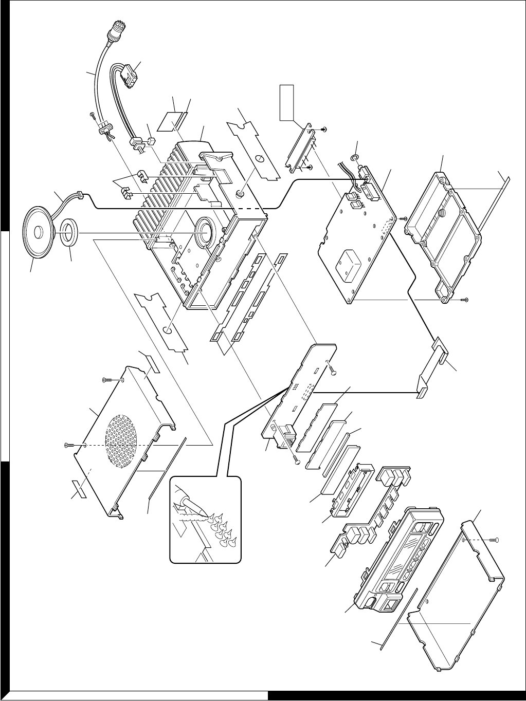
42
TK-760G/762G
EXPLODED VIEW (TK-760G)
Parts with the exploded numbers larger than 700 are not supplied.
1
2
ABC
1
24
3
24
2
40 37
7
11
6
17
22
22
23x2
27
24
9
25 14
12
21x2
44
26
IC400
16
701
702
Cx2
703
A
C
C
Cx2
Dx11
B
B
A
Ax2
703
TX-RX unit
(X57-595) (B/2)
TX-RX unit
(X57-595) (A/2)
Display unit
(X54-327)
704
A M2.6 x 6 (OC) BLK : N33-2606-45
B M3 x 8 : N67-3008-46
C M2.6 x 6 (Br-Tap) : N87-2606-46
D M2.6 x 12 (Br-Tap) : N87-2612-46
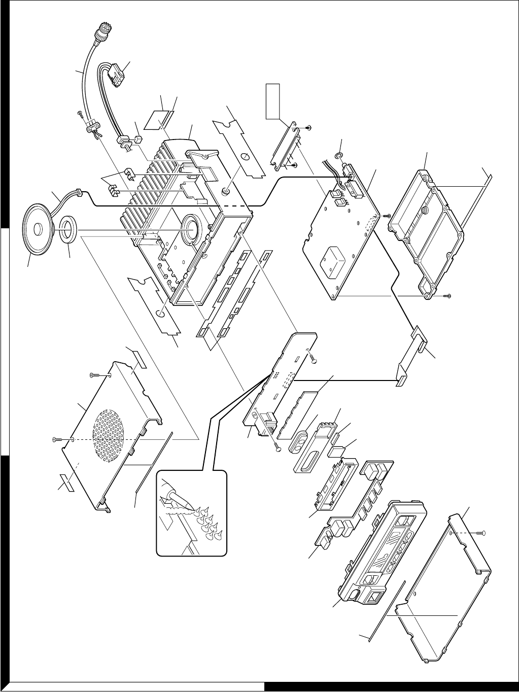
43
TK-760G/762G
EXPLODED VIEW (TK-762G)
1
2
DEF
1
24
3
24
2
40 37
11
6
7
28
17
22
22
23x2
27
24
9
25 14
12
21x2
44
26
IC400
16
701
702
Cx2
703
C
C
Cx2
Dx11
B
B
A
A
Ax2
703
TX-RX unit
(X57-595) (B/2)
TX-RX unit
(X57-595) (A/2)
Display unit
(X54-328)
704
A M2.6 x 6 (OC) BLK : N33-2606-45
B M3 x 8 : N67-3008-46
C M2.6 x 6 (Br-Tap) : N87-2606-46
D M2.6 x 12 (Br-Tap) : N87-2612-46
Parts with the exploded numbers larger than 700 are not supplied.
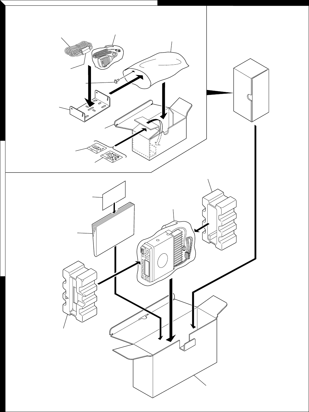
44
TK-760G/762G
PACKING
Parts with the exploded numbers larger than 700 are not supplied.
GH
1
2
3
5 Cap
(B09-0235-05)
8 Instruction manual
(B62-1257-10) : M
(B62-1258-00) : K,K2
705 Warranty card
13 DC cord
(E30-3339-05)
19 Fuse (10A)
(F51-0016-05) x 2
30 Polystyrene foamed fixture (F)
(H10-6618-12)
31 Polystyrene foamed fixture (R)
(H10-6619-12)
32 Inner packing case
(H12-1391-03)
33 Protection bag
(H25-0720-04)
33 Protection bag
(H25-0720-04)
34 Item carton case
(H52-1519-02)
36 Holder
(J19-1584-05)
38 Bracket
(J29-0627-23)
42 Screw set
(N99-0395-05)
45 Microphone
(T91-0597-15) : K,K2
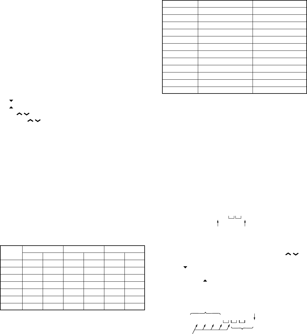
45
TK-760G/762G
ADJUSTMENT
Test Mode (TK-760G Only)
■Test Mode Operating Features
This transceiver has a test mode.
To enter test mode,
press [SCN] key and turn power on. Hold [SCN] key un-
til test channel No. and test signalling No. appears on
LCD.
Test mode can be inhibited by programming. To exit
test mode, switch the power on again. The following func-
tions are available in test mode.
• Controls
[PTT] Used when making a transmission.
[MON] Monitor on and off.
[SCN] Sets to the tuning mode.
[A] Function on.
[D/A] RF power high and low.
[] Changes signalling.
[] Changes wide and narrow
[CH /] Changes channel.
[Volume /] Volume up/down.
• LCD indicator
"SCN" Unused.
"AUX" Lights at RF power low.
"MON" Lights at monitor on.
"Right side dot" Lights at narrow.
• LED indicator
Red LED Lights during transmission.
Green LED Lights when there is a carrier.
■Frequency and Signalling
The set has been adjusted for the frequencies shown in
the following table. When required, re-adjust them follow-
ing the adjustment procedure to obtain the frequencies you
want in actual operation.
• Frequency (MHz)
Channel TK-760G/762G (K)
TK-760G/762G (K2)
TK-760G (M)
No. RX TX RX TX RX TX
1 (Center)
161.050 161.100 149.050 149.100 160.050 160.100
2 (Low) 148.050 148.100 136.050 136.100 146.050 146.100
3 (High) 173.950 173.900 161.950 161.900 173.950 173.900
4 161.000 161.000 149.000 149.000 160.000 160.000
5 161.200 161.200 149.200 149.200 160.200 160.200
6 161.400 161.400 149.400 149.400 160.400 160.400
7~16 ––––––
• Signalling
Signalling No. RX TX
1 None None
2 None 100Hz square
3 QT 67.0Hz QT 67.0Hz
4 QT 151.4Hz QT 151.4Hz
5 QT 210.7Hz QT 210.7Hz
6 QT 250.3Hz QT 250.3Hz
7 DQT D023N DQT D023N
8 DQT D754I DQT D754I
9 DTMF DEC, (159D) DTMF ENC, (159D)
10 None DTMF tone (9)
11 2-tone 321.7/928.1Hz None
12 Single tone 1200Hz Single tone 1200Hz
• Preparations for tuning the transceiver
Before attempting to tune the transceiver, connect the
unit to a suitable power supply.
Whenever the transmitter is turned, the unit must be
connected to a suitable dummy load (i.e. power meter).
The speaker output connector must be terminated with a
4Ω dummy load and connected to an AC voltmeter and an
audio distortion meter or a SINAD measurement meter at all
times during tuning.
• Transceiver tuning
(To place transceiver in tuning mode)
Channel appears on LCD. Set channel according to tun-
ing requirements.
LCD display (Test mode)
11
–
Channel No. Signalling No.
Press [SCN], now in tuning mode. Use [D/A] button to
write tuning data through tuning modes, and [CH /] to
adjust tuning requirements (1 to 256 appears on LCD).
Use [ ] button to select the adjustment item through
tuning modes. Use [A] button to adjust 3-point or 5-point
tuning, and use [ ] button to switch between wide/narrow.
LCD display (Tuning mode)
FREQ1
Adjustment
(1~256)
Adjustment item
..... .
Point tuning indicator
Wide/Narrow indicator
Off : Wide
On : Narrow
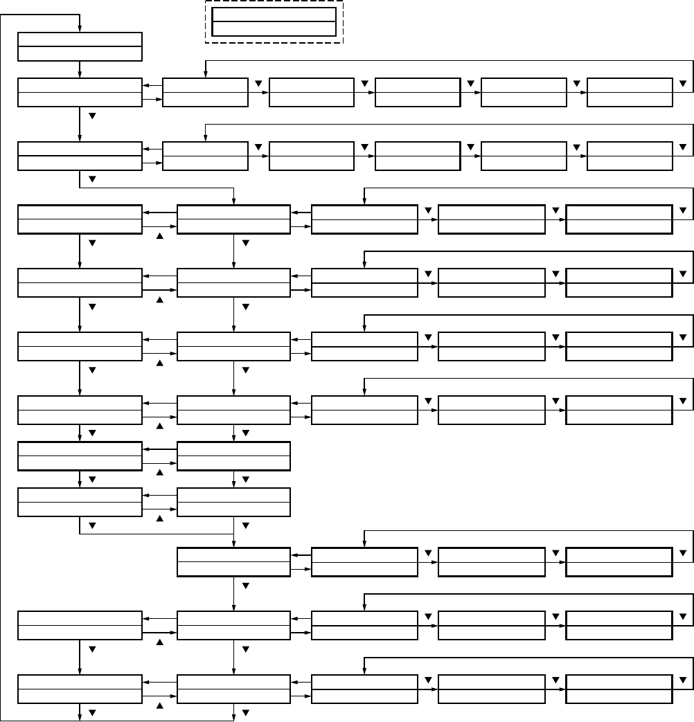
46
TK-760G/762G
FREQ_ _XX
Frequency adj.
Display
Function name
HPOW_XXX
RF high power
H.POW_XXX
Hi power (L)
H.P.OW_XXX
Hi power (L')
[A] [D/A] [D/A] [D/A] [D/A] [D/A]
H.P.O.W_XXX
Hi power (C)
H.P.O.W._XXX
Hi power (H')
H.P.O.W._.XXX
Hi power (H)
LPOW_XXX
RF low power
L.POW_XXX
Low power (L)
L.P.OW_XXX
Low power (L')
[A]
L.P.O.W_XXX
Low power (C)
L.P.O.W._XXX
Low power (H')
L.P.O.W._.XXX
Low power (H)
_MAX_XXX
Max deviation (Wide)
_.MAX_XXX
Max deviation (L)
_MAX_ XXX.
Max deviation (Narrow) [A]
_.M.A.X_XXX
Max deviation (C)
_.M.A.X._.XXX
Max deviation (H)
WIDENARROW
_BAL_XXX
DQT balance (Wide)
_.BAL_XXX
DQT balance (L)
_BAL_XXX.
DQT balance (Narrow) [A]
_.B.A.L_XXX
DQT balance (C)
_.B.A.L._.XXX
DQT balance (H)
_FQT_XXX
QT fine deviation (Wide)
_.FQT_XXX
QT fine deviation (L)
_FQT_ XXX.
QT fine deviation (Narrow)
[A]
_.F.Q.T_XXX
QT fine deviation (C)
_.F.Q.T._.XXX
QT fine deviation (H)
FDQT_XXX
DQT fine deviation (Wide)
F.DQT_XXX
DQT fine deviation (L)
FDQT_XXX.
DQT fine deviation (Narrow)
[A]
F.D.Q.T_XXX
DQT fine deviation (C)
F.D.Q.T._.XXX
DQT fine deviation (H)
SENS_XXX
Seisitivity
S.ENS_XXX
Sensitivity (L)
[A]
S.E.N.S_XXX
Sensitivity (C)
S.E.N.S._.XXX
Sensitivity (H)
DTMF_XXX
DTMF fine deviation (Wide)
DTMF_XXX.
DTMF fine deviation (Narrow)
TONE_XXX
Single tone fine deviation (Wide)
TONE_XXX.
Single tone fine deviation (Narrow)
WIDENARROW
[ ]
[ ]
[ ]
[ ]
[ ]
[ ] [ ]
[ ] [ ]
[ ]
[ ] [ ]
[ ]
[ ] [ ]
[ ]
[ ] [ ]
[ ]
[ ] [ ]
[ ]
[ ] [ ] [ ] [ ]
[D/A] [D/A]
[D/A] [D/A] [D/A]
[D/A] [D/A] [D/A]
[ ] [ ]
[ ] [ ] [ ]
[D/A] [D/A] [D/A]
[D/A] [D/A] [D/A]
[D/A] [D/A] [D/A]
[D/A] [D/A] [D/A]
[D/A] [D/A] [D/A]
[D/A] [D/A] [D/A]
[ ] [ ] [ ]
[ ] [ ] [ ]
SQL3_XXX
Squelch (Open) (Wide)
S.QL3_XXX
Squelch (Open) (L)
SQL3_XXX.
Squelch (Open) (Narrow) [A]
S.Q.L.3_XXX
Squelch (Open) (C)
S.Q.L.3._.XXX
Squelch (Open) (H)
[ ]
[ ] [ ]
[ ] [ ] [ ]
SQL9_XXX
Squelch (Tight) (Wide)
S.QL9_XXX
Squelch (Tight) (L)
SQL9_XXX.
Squelch (Tight) (Narrow) [A]
S.Q.L.9_XXX
Squelch (Tight) (C)
S.Q.L.9._.XXX
Squelch (Tight) (H)
[ ]
[ ] [ ]
[ ] [ ] [ ]
[ ] [ ] [ ]
[ ] [ ] [ ]
[ ] [ ] [ ]
■Tuning Mode
ADJUSTMENT
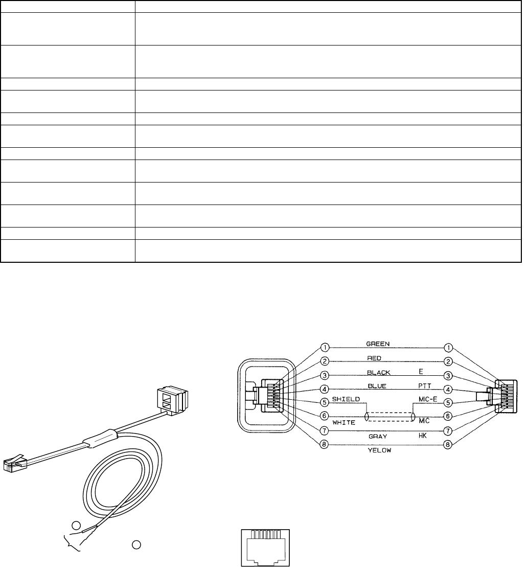
47
TK-760G/762G
Test Equipment Required for Alignment
Test Equipment Major Specifications
1. Standard Signal Generator Frequency Range 136 to 174MHz
(SSG) Modulation Frequency modulation and external modulation
Output –127dBm/0.1µV to greater than –7dBm/100mV
2. Power Meter Input Impedance 50Ω
Operation Frequency 136 to 174MHz or more
Measurement Capability Vicinity of 100W
3. Deviation Meter Frequency Range 136 to 174MHz
4. Digital Volt Meter Measuring Range 1 to 20V DC
(DVM) Accuracy High input impedance for minimum circuit loading
5. Oscilloscope DC through 30MHz
6. High Sensitivity Frequency Range 10Hz to 1000MHz
Frequency Counter Frequency Stability 0.2ppm or less
7. Ammeter 20A
8. AF Volt Meter Frequency Range 50Hz to 10kHz
(AF VTVM) Voltage Range 1mV to 10V
9. Audio Generator (AG) Frequency Range 20Hz to 20kHz or more
Output 0 to 1V
10. Distortion Meter Capability 3% or less at 1kHz
Input Level 50mV to 10Vrms
11. 4Ω Dummy Load Approx. 4Ω, 10W or more
12. Regulated Power Supply 13.6V, approx. 20A (adjustable from 9 to 20V)
Useful if ammeter requipped
ADJUSTMENT
Lead wire +
MIC Shield wire –
1
8
Tuning cable (E30-3383-05)
Adapter cable (E30-3383-05) is required for
injecting an audio if PC tuning is used.
See "PC Mode" section for the connection.
MIC connector
(Front view)
Test cable for microphone input (E30-3360-08)
1 : BLC
2 : PSB
3 : E
4 : PTT
5 : ME
6 : MIC
7 : HOOK
8 : CM
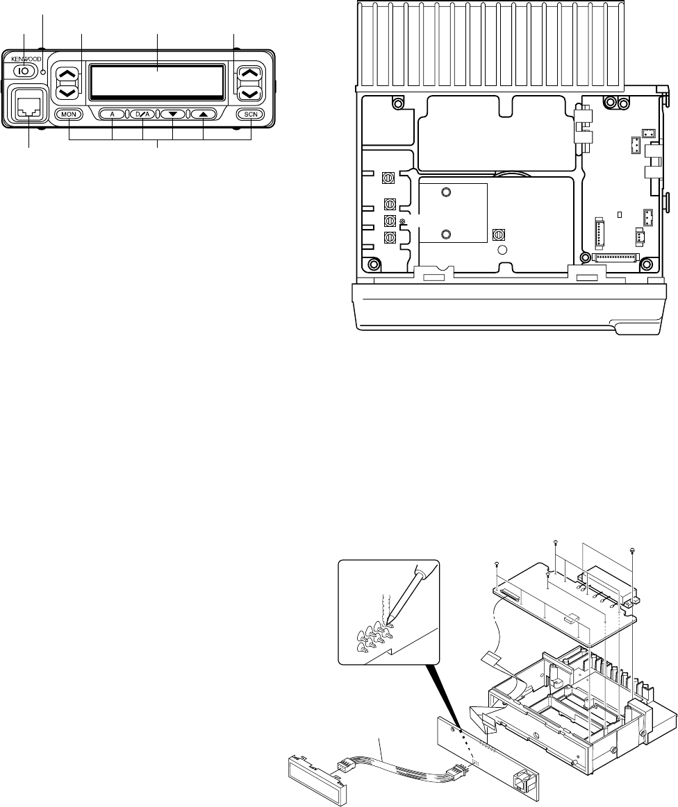
48
TK-760G/762G
ADJUSTMENT
Adjustment Location
■Switch (TK-760G)
■Adjustment Point
■Note
• Flash memory
The firmware program (User mode, Test mode, Tuning
mode, etc.) and the data programmed by the FPU (KPG-56D)
for the flash memory, is stored in memory. When parts are
changed, program the data again.
• EEPROM
The tuning data (Deviation, Squelch, etc.) for the
EEPROM, is stored in memory. When parts are changed,
readjust the transceiver.
■Repair Jig
• Chassis
Use jig (Part No. : A10-4010-02) for repairing the TK-
760G/762G. The jig facilitates the voltage check when the
voltage on the component side TX-RX unit is checked during
repairs.
• Extension cable
Part No. : E30-3404-05
L13
L11
L18
L15
L5
IC5 9pin
RSSI
TX-RX UNIT (A/2)
PLL/VCO
TC106
CV
TC109
Power
LED Volume
up/down Display
Channel
up/down
MIC jack Programmable function keys
Ax4
Ax5
Extension cable
Ax2
Bx2
Aø2.6 x 6
B M3 x 8
49
ADJUSTMENT
Measurement
Test-
equipment Unit Terminal
Adjustment
Unit Parts Method Specifications/RemarksConditionItem
TK-760G/762G
Receiver Section
1.
Discriminator
1) Set test mode SSG Rear ANT TX-RX L5
AF output maximum.
• Wide CH : CH1 - Sig1 panel (A/2)
SSG output : –53dBm/501µV AF VTVM ACC
SSG MOD : 3kHz
Oscilloscope
(EXT.SP)
AF : 1.4V/4Ω
2) SSG MOD : OFF DVM TX-RX IC5 9pin 0.7V DC
(A/2)
2. Sensitivity 1) Set test mode SSG Rear ANT TX-RX L11 RSSI voltage
• Wide
Select “SENS” in tuning mode.
panel (A/2) L13 maximum.
“S.E.N.S” AF VTVM ACC L15
Adjust [120] K,M Distortion (EXT.SP) L18
Adjust [110] K2 meter
SSG freq'
Oscilloscope
: 161.050MHz KAG
: 149.050MHz K2
: 160.050MHz MDVM TX-RX RSSI
SSG output : –118dBm/0.28µV
(A/2)
SSG MOD : 3kHz
AF output : 1V/4Ω
2) “S.ENS” Front
CH /
Adjust [***] panel
SSG freq' .
: 148.050MHz K
: 136.050MHz K2
: 146.050MHz M
3) “S.E.N.S._.”
Adjust [***]
SSG freq'
: 173.950MHz K,M
: 161.950MHz K2
Measurement
Test-
equipment Unit Terminal
Adjustment
Unit Parts Method Specifications/RemarksConditionItem
1. PLL lock 1) Set test mode DVM TX-RX CV PLL TC106 7.5V K,M ±0.1V
voltage CH : CH3 - Sig1
Power meter
(A/2) 7.0V K2
RX F. conter
TX 2) PTT : ON (Transmit) TC109 7.5V
RX 3) CH : CH2 - Sig1 Check 1.0V or more K,M
AUX : ON (talk-around mode) 0.9V or more K2
TX 4) PTT : ON (Transmit) 0.5V or more K,M
1.0V or more K2
Common Section Since the TK-762G cannot be tuned from the panel, the FPU (KPG-56D) should be used for adjustment.

ADJUSTMENT
Measurement
Test-
equipment Unit Terminal
Adjustment
Unit Parts Method Specifications/RemarksConditionItem
50
TK-760G/762G
3. Squelch 3 1) Set test mode SSG Rear ANT Front
CH /
Adjust to the
• Wide
Select “SQL3” in tuning mode.
panel panel squelch threshold
“S.QL3” AF VTVM ACC point.
Adjust [***] Distortion (EXT.SP)
SSG freq' meter
: 148.050MHz K
Oscilloscope
: 136.050MHz K2 AG
: 146.050MHz M
SSG output : –127dBm/0.1µV
SSG MOD : 3kHz (Wide)
1.5kHz (Narrow)
2) “S.Q.L.3”
Adjust [***]
SSG freq'
: 161.050MHz K
: 149.050MHz K2
: 160.050MHz M
3) “S.Q.L..3._.”
Adjust [***]
SSG freq'
: 173.950MHz K,M
: 161.950MHz K2
• Narrow 4) “SQL3***.”
Adjust [***]
SSG freq'
: 161.050MHz K
: 149.050MHz K2
: 160.050MHz M
4. Squelch 9 1) Set test mode
• Wide
Select “SQL9” in tuning mode.
“S.QL9”
Adjust [***]
SSG freq'
: 148.050MHz K
: 136.050MHz K2
: 146.050MHz M
SSG output : –114dBm/0.44µV
SSG MOD : 3kHz (Wide)
1.5kHz (Narrow)
2) “S.Q.L.9”
Adjust [***]
SSG freq'
: 161.050MHz K
: 149.050MHz K2
: 160.050MHz M
3) “S.Q.L.9._.”
Adjust [***]
SSG freq'
: 173.950MHz K,M
: 161.950MHz K2
• Narrow 4) “SQL9***.”
Adjust [***]
SSG freq'
: 161.050MHz K
: 149.050MHz K2
: 160.050MHz M
5. Squelch 1) Set test mode Check Squelch must be opened.
check CH : CH1 - Sig1~CH3 - Sig1 (Wide/Narrow)
SSG output : –118dBm/0.28µV
2) SSG output : OFF Squelch must be closed.
(Wide/Narrow)
51
ADJUSTMENT
Measurement
Test-
equipment Unit Terminal
Adjustment
Unit Parts Method Specifications/RemarksConditionItem
TK-760G/762G
6. QT check 1) Set test mode SSG Rear ANT
CH : CH1 - Sig4 panel
SSG MOD AF VTVM ACC
INT : 3kHz (Wide), 1.5kHz (Narrow)
Distortion (EXT.SP)
EXT : 151.4Hz meter
SSG system MOD DEV
Oscilloscope
:
±3.75kHz (Wide), ±1.85kHz (Narrow)
AG
SSG output : 10dB SINAD level
2) CH : CH1 - Sig3 Check Squelch must be opened.
CH1 - Sig5
CH1 - Sig6
Measurement
Test-
equipment Unit Terminal
Adjustment
Unit Parts Method Specifications/RemarksConditionItem
1. Frequency 1) Set test mode
Power meter
Rear ANT Front
CH /
Check 161.100MHz±50Hz K
Select “FREQ” in tuning mode.
F. counter panel panel 149.100MHz±50Hz K2
PTT : ON 160.100MHz±50Hz M
Adjust [_**]
2. Power 1) Maximum power Check More than 28.0W
output Set test mode
Select “HPOW” in tuning mode.
“H.POW”
Adjust [256]
PTT : ON
3. High power 1) Set test mode 25.0W ±1.0W
Select "HPOW" in tuning mode.
“H.POW”
PTT : ON
Adjust [***]
2) “H.P.OW”
PTT : ON
Adjust [***]
3) “H.P.O.W”
PTT : ON
Adjust [***]
4) “H.P.O.W.”
PTT : ON
Adjust [***]
5) “H.P.O.W._.”
PTT : ON
Adjust [***]
4. Low power 1) Set test mode
Power mete
5.0W ±0.5W
Select “LPOW” in tuning mode.
“L.POW”
PTT : ON
Adjust [***]
2) “L.P.OW”
PTT : ON
Adjust [***]
Transmitter Section
ADJUSTMENT
Measurement
Test-
equipment Unit Terminal
Adjustment
Unit Parts Method Specifications/RemarksConditionItem
52
TK-760G/762G
3) “L.P.O.W”
Power meter
Rear ANT Front
CH /
5.0W ±0.5W
PTT : ON panel panel
Adjust [***]
4) “L.P.O.W.”
PTT : ON
Adjust [***]
5) “L.P.O.W._.”
PTT : ON
Adjust [***]
5. Power check 1) Set test mode
Power meter
Rear ANT Check 25W±1W, 8A or less
CH : CH1 - Sig1 panel
CH2 - Sig1 Ammeter DC IN
CH3 - Sig1
PTT : ON
6. Modulation 1) Set test mode
Power meter
Rear ANT Front
CH /
Make the de- (Wide/Narrow)
balanced MIC input : OFF Deviation panel panel modulation
• Wide Select “BAL” in tuning mode. meter waveform neat.
“_.BAL”
Oscilloscope
Deviation meter filter
LPF : 3kHz, HPF : OFF AF VTVM Front MIC
De-emphasis : OFF AG panel
PTT : ON
Adjust [***]
2) “_.B.A.L”
PTT : ON
Adjust [***]
3) “_.B.A.L._.”
PTT : ON
Adjust [***]
• Narrow 4) “_BAL***.”
PTT : ON
Adjust [***]
7. Maximum 1) Set test mode 3.95kHz (Wide) ±50Hz (Wide/Narrow)
deviation Connect AG to the MIC 1.95kHz (Narrow)
• Wide terminal. (According to the
Select “MAX” in tuning mode.
larger +, –)
“_.MAX”
AG : 1kHz/50mV
Deviation meter filter
LPF : 15kHz, HPF : OFF
De-emphasis : OFF
PTT : ON
Adjust [***]
2) “_.M.A.X”
PTT : ON
Adjust [***]
3) “_.M.A.X._.”
PTT : ON
Adjust [***]
• Narrow 4) “_MAX***.”
PTT : ON
Adjust [***]
53
ADJUSTMENT
Measurement
Test-
equipment Unit Terminal
Adjustment
Unit Parts Method Specifications/RemarksConditionItem
TK-760G/762G
8. MIC 1) Set test mode
Power meter
Rear ANT Check ±3kHz±0.2kHz (Wide)
seisitivity CH : CH1 - Sig1 Deviation panel ±1.5kHz±0.05kHz (Narrow)
check AG : 1kHz/5mV meter
PTT : ON
Oscilloscope
Adjust [***]
AF VTVM Front MIC
9. QT deviation 1) Set test mode AG panel Front
CH /
0.75kHz ±50Hz (Wide/Narrow)
• Wide
Select “FQT” in tuning mode.
panel
“_.FQT”
Deviation meter filter
LPF : 3kHz, HPF : OFF
PTT : ON
Adjust [***]
2) “_.F.Q.T”
PTT : ON
Adjust [***]
3) “_.F.Q.T._.”
PTT : ON
Adjust [***]
• Narrow 4) “_FQT***.” 0.35kHz
PTT : ON
Adjust [***]
10. DQT 1) Set test mode Front
CH /
0.75kHz ±50Hz (Wide/Narrow)
deviation
Select “FDQT” in tuning mode.
panel
• Wide “F.DQT”
Deviation meter filter
LPF : 3kHz, HPF : OFF
PTT : ON
Adjust [***]
2) “F.D.Q.T”
PTT : ON
Adjust [***]
3) “F.D.Q.T._.”
PTT : ON
Adjust [***]
• Narrow 4) “FDQT***.” 0.35kHz
PTT : ON
Adjust [***]
11. DTMF 1) Set test mode Front
CH /
3.0kHz ±0.2kHz
deviation
Select “DTMF” in tuning mode.
panel
• Wide Deviation meter filter
LPF : 15kHz, HPF : OFF
PTT : ON
Adjust [***]
• Narrow 2) “DTMF***.” 1.5kHz ±0.1kHz
PTT : ON
Adjust [***]
12. TONE 1) Set test mode Front
CH /
3.0kHz ±0.1kHz (Wide/Narrow)
deviation
Select “TONE” in tuning mode.
panel
• Wide Deviation meter filter
LPF : 15kHz, HPF : OFF
PTT : ON
Adjust [***]
• Narrow 2) “TONE***.” 1.5kHz
PTT : ON
Adjust [***]
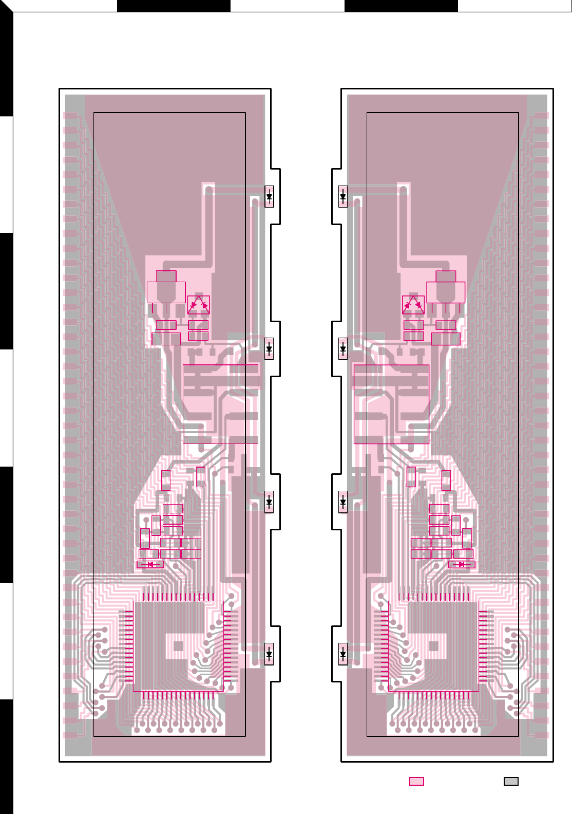
54
TK-760G/762G
ACE
BD
1
3
5
7
2
4
6
TK-760G/762G PC BOARD VIEWS
DISPLAY UNIT (X54-3270-10) : TK-760G
Component side view
DISPLAY UNIT (X54-3270-10) : TK-760G
Foil side view
D804 D803 D805 D802
J72-0683-02
CN801
MBL
5C
CE
CL
E
E
SB
DI
12
78
C801
C802
C803
C804
C805
C806 C807
D801
D808
IC801
B
C
E
Q801
R801
R802
R803
R804
R805
R806
R808
R809
L801
1
16
17
32
48
49 64
33
D804 D803 D805 D802
J72-0683-02
CN801
1 MBL
5C
CE
CL
E
E
SB
DI
2
78
C801
C802
C803
C804
C805
C806
C807
D801
D808
IC801
B
C
E
Q801
R801
R802
R803
R804 R805
R806
R808 R809
L801
1
16
17 32
48
49
64
33
Component side Foil side
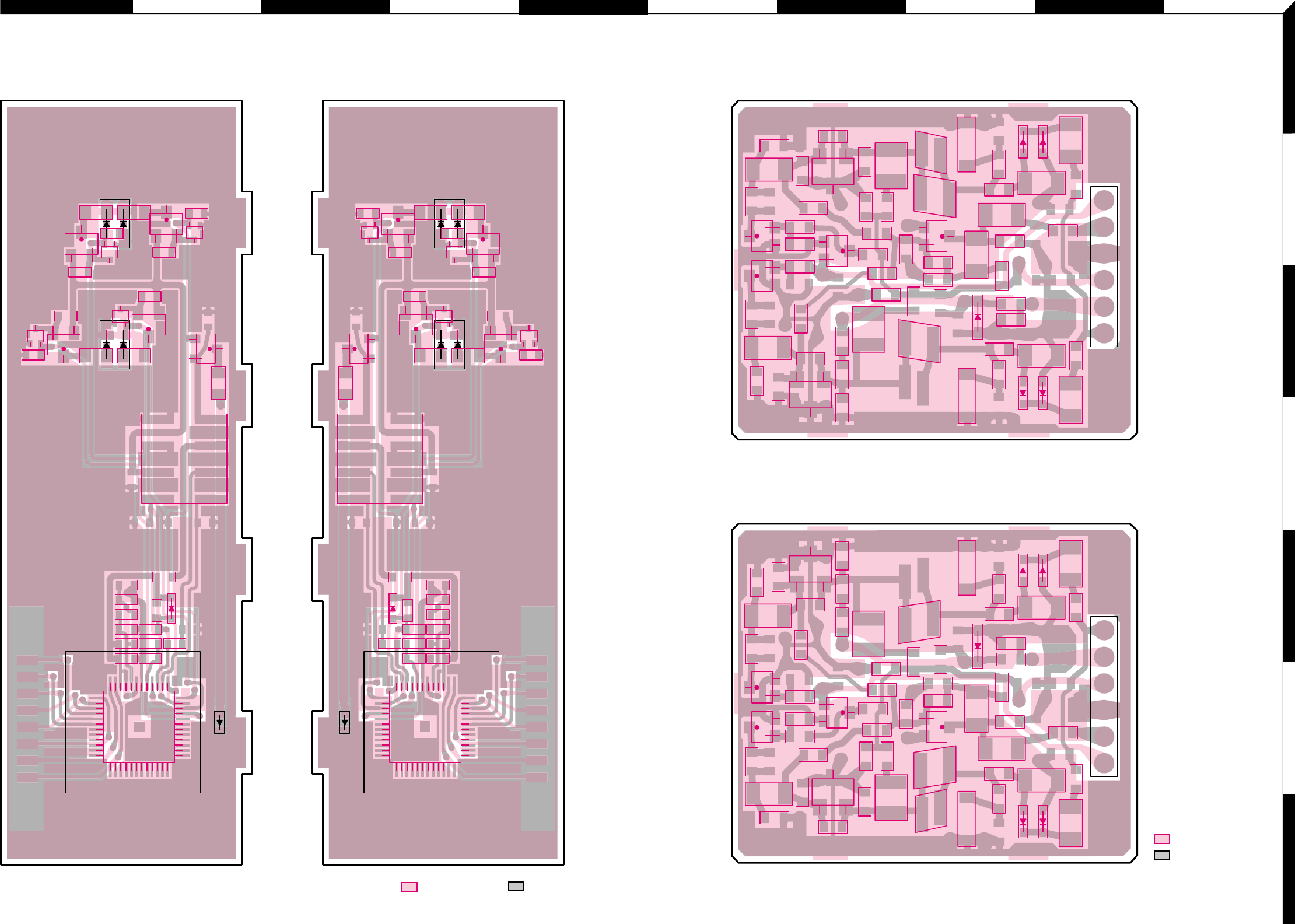
J
H
FD
BI
G
E
C
A
1
3
5
7
2
4
6
55 56
PC BOARD VIEWS TK-760G/762G
Component side
Foil side
D801
D804
D803
J72-0684-02
CN801
1
MBL
5C
CE
CL
E
E
SB
DI
2
78
IC801
1
12
13
24
36
37 48
25
R803
R805
Q801
Q802
Q803
Q805
R810 R809
C801
C806
C808
C812
R812
R804
C804
R802
C803
C802
R801
R808
C807
C805
R806
D802
R807
L801
Q804
Q806
Q807
G
SD
G
S
D
G
S
D
G
SD
Q808
Q809
R813
R814
R815
R816
D801
D804
D803
J72-0684-02
CN801
1MBL
5C
CE
CL
E
E
SB
DI
2
78
IC801
1
12
13 24
36
3748
25
R803 R805
Q801
Q802
Q803
Q805
R810
R809
C801
C806
C808
C812
R812
R804
C804
R802
C803
C802
R801
R808
C807
C805
R806
D802
R807
L801
Q804
Q806
Q807
G
SD
G
SD
G
S
D
G
S
D
Q808
Q809
R813
R814
R815
R816
CN101
RX
(ST) 6
1
HT
E
8CL
MD
CV
J72-0676-02
C107
C114
C121
C118
C111
C123
C117
D105
R116
C110
R101 R102
TC106
L101
TC109
R117
R106
R104
R105
C113
C124
R112
R113
L102
C112
D101 D102
D103 D104
L108
L107
Q101
G
S
D
G
S
DQ103
L105
L103
L104
C102
C126
C120
C119
R110
C125
R107
C115
C104
C105
R103
R108
C116
L110
L109
C122
R115
R109
R114
R111
Q102
Q104
Q105
Q106
L106
C127
L111
L112
L116
CN101
RX
(ST)
HT
E
8CL
MD
CV 1
6
J72-0676-02
L103
L104
C102
C126
C120
C119
R110
C125
R107
C115
C104
C105
R103
R108
C116
L110
L109
C122
R115
R109
R114
R111
Q102
Q104
Q105
Q106
L106
C127
L111
L112
L116
C107
C114
C121
C118
C111
C123
C117
D105
R116
C110
R101
R102
TC106
L101
TC109
R117
R106
R104
R105
C113
C124
R112 R113
L102
C112
D101
D102
D103
D104
L108
L107
Q101
G
S
D
G
S
D
Q103
L105
PLL/VCO (X58-4670-XX) -10 : K,M -11 : K2 Component side view
PLL/VCO (X58-4670-XX) -10 : K,M -11 : K2 Foil side view
DISPLAY UNIT (X54-3280-10) : TK-762G
Component side view
DISPLAY UNIT (X54-3280-10) : TK-762G
Foil side view
Component side Foil side
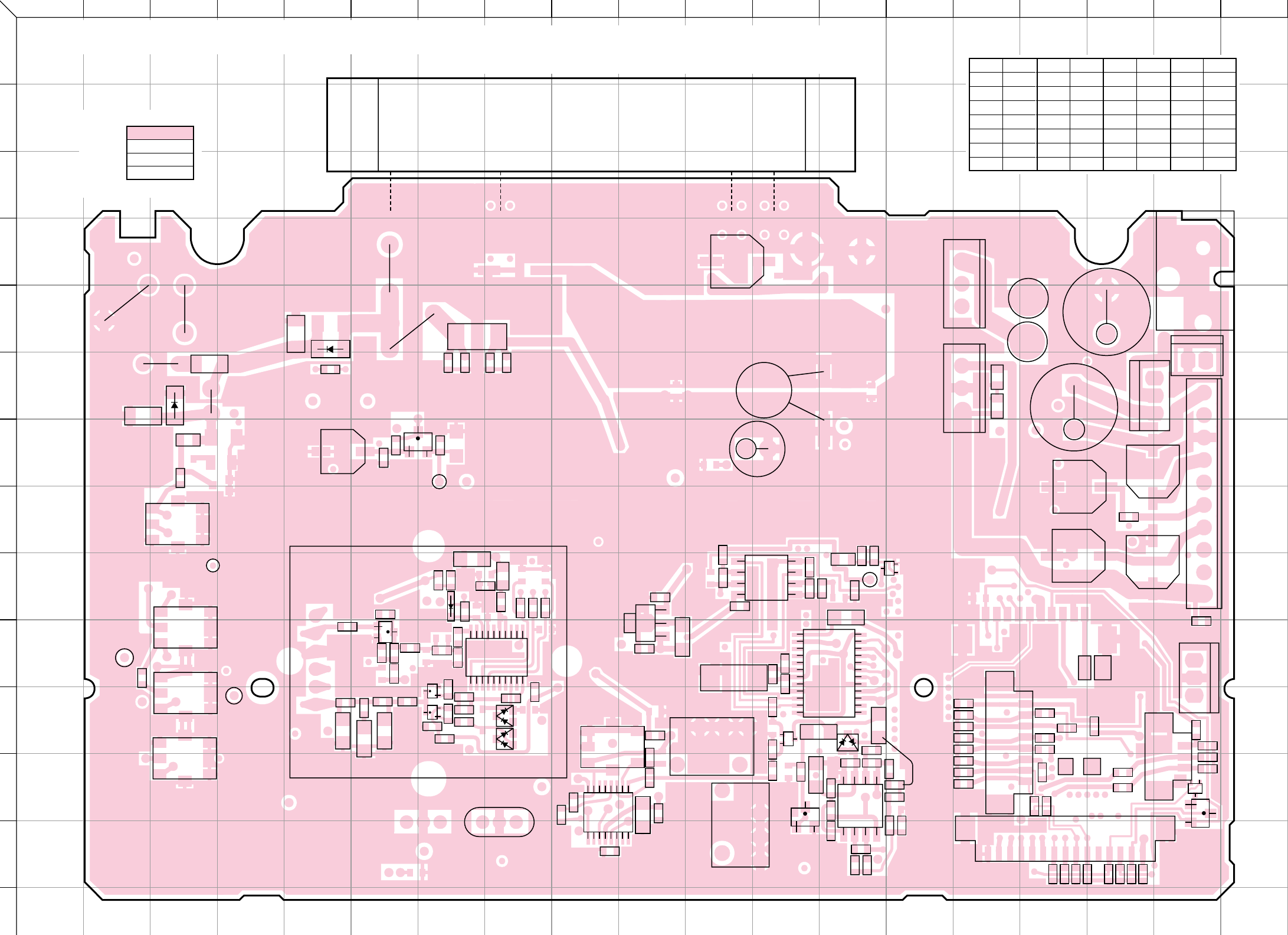
ABCDEFGH IJ
KLM
NOPQRS
1
2
3
4
5
6
7
8
9
10
11
12
13
14
C91
C67
D12
D13
R93
C104
Q32
L24
L20
L25
IC5
IC6
IC3
C10
C7
C3
C60
C107
C75
Q9
C54
XF1
CN4
CN5
C50
C131
C117
C161
C160
R68
C74
C46
C43
R44
IC4
R78
IC7
C103
C98
C81
R71
Q12
C89
C93
C99
C1
C5
C8
C11
C2
C6
C9
C12
C141
C144
C134
IC12
C39
C32
C203
C207
C210
C212
L18
C213
L15
C138
D33
C211
L13
L11
C86
C64
CF2
CF1
R87C96
C97
C16
C17
C18
C19
C21
C15
C14
C13
R9
R10
R11
R59
C72
Q2
R91
R37
R34
R56
R86
D9
C40
R53
R52
R51
C84
IC11
R8
R7
R2
R66 R49
R40
TH1
R5
R6
R177
R62
R57
C61
R1
R3
R4
C45
C70
R50
R75
C165
R131
C79
C80
R67
R63
R48
R89
R77
R90
R64
R70
Q11
R65
R79R82
R85
R27
L21
C198
C214
D34
L22
C171
C208
R76C83
IC13
C166
C172
C114
C195
C30
C35
C47
C63
L23
Q8
R188
Q37
R193
D40
L26
R202
R201
Q38
R197
L5
C261
C260
R195
Q39
C77
D25
R19
Q35
R208
TV
8R
CV
J72-0677-02 A/2
+
+
+
A1 : X58-4670-XX
8CL
+
+
1
1011
20
1
89
16
+
G
O
I
+
+
+
+
+
+
1
45
8
+
1
1213
24
+
+
+
G
DS
5C
G
SD
1
45
8
SB
GND
DEO
DTC
IGN
DI
ME
MI
PTT
SQ
1
8
RSSI
GND
E
C
B
O
G
I
GND
B
+
+
J1
EXT. SP
CN7
1
3
PA/LI
SPI
SPO
CN8
2
1
E
10 SP
+
+
CN3
SB
E
HOR
3
1
1
1
3
AM
MM
EMG/TXS
G
DS
CN1
15
1
GND
MIO
MII
AFI
AFO
ALT
AUX2
AUX4
AUX1
AUX3
NC
AUX6
AUX5
5S
8C
12 34
IC400
RX
(ST)
HT
E
8CL
MD
CV
Component side
Foil side
Pattern 1
Pattern 2
Pattern 3
Pattern 4
TK-760G/762G PC BOARD VIEW TX-RX UNIT (X57-5950-XX) (A/2) Component side view
-10 : TK-760G K -11 : TK-762G K -12 : TK-760G K2
-13 : TK-762G K2 -21 : TK-760G M
Ref. No.
Address
IC3 10H
IC4 12M
IC5 12I
IC6 10M
IC7 9L
IC11 10J
IC12 6O
Ref. No.
Address
IC13 8R
IC400 2I
Q2 12R
Q8 7G
Q9 10F
Q11 11G
Q12 11G
Ref. No.
Address
Q32 4O
Q35 12L
Q37 11L
Q38 12R
Q39 9N
D9 9G
D12 11H
Ref. No.
Address
D13 11H
D25 6L
D33 6C
D34 5E
D40 11M
57
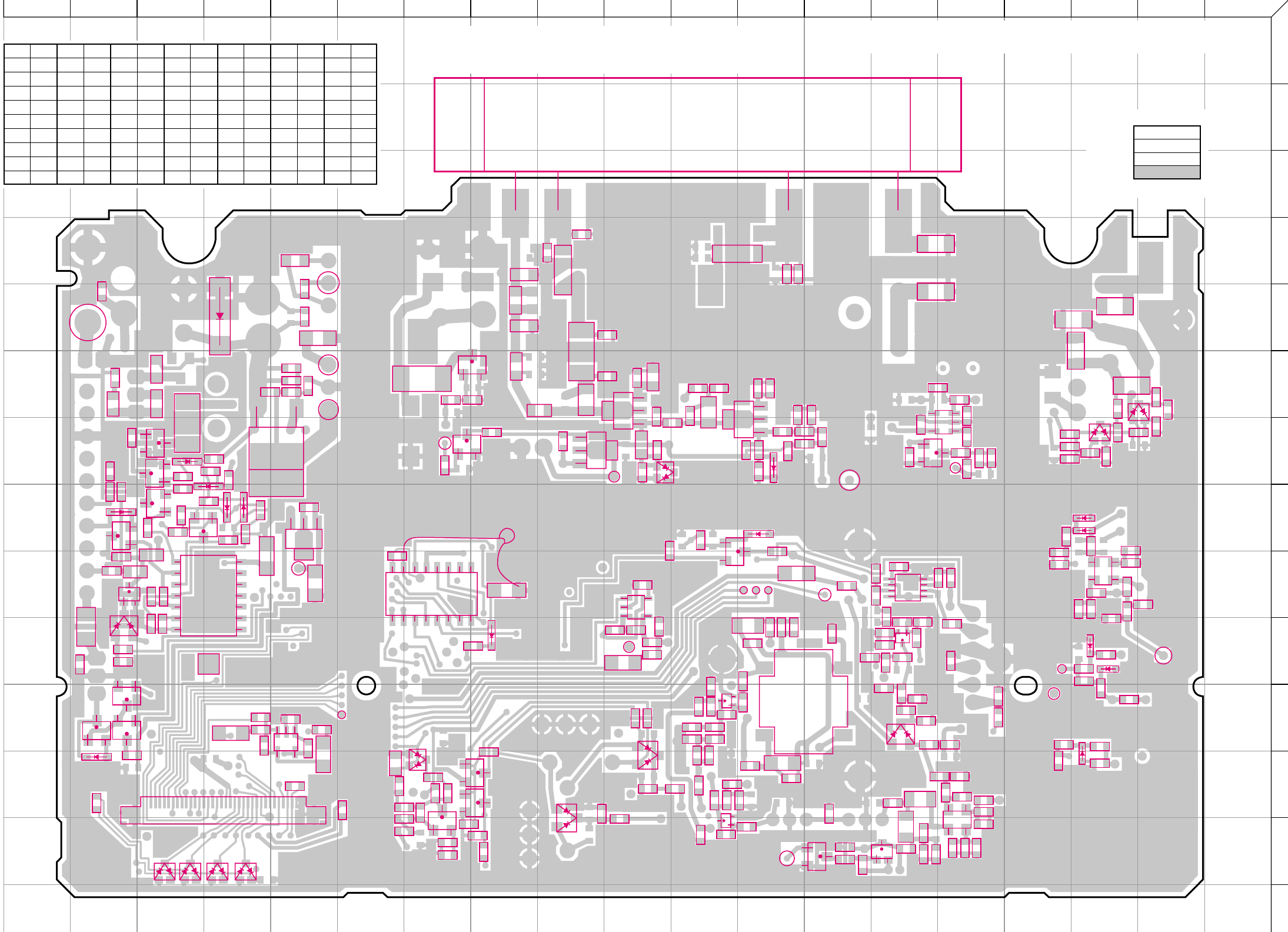
S
RQP
O
NMLK
J
IHGF
E
D
CB
A
1
2
3
4
5
6
7
8
9
10
11
12
13
14
R155
R160
DB
8C
SB
D22
C92
C94
C95
R69
L17
IC14
R123
R95
C200
C156
R133
Q23
C221
C205
C148
C222
C274
R170
D29
C179
D2
Q1
D24
C4
R29
R151
C142
C174
R108
R113
C139
C168
R137
C151
R121
C147
C170
D17
C162
C159
R101
R98
C112
C115
C118
C120
R106
R92
UL
C125
R148
R146
R150
Q4
D3
D4
D5
R13
Q6
D14
Q17
C106
Q13
C88
D11
R43 C37
C66
R61
C69
D1
R22
C121
C119
C190
C157
C180
R115
Q29
R178
C123
R107
R136
Q24
C186
Q19
SP
C128
C116
C113
IC10
Q21
R175
C204
C196
C217
C223
R169
IC15
D36
D35
C224
C220
R157
C183
C187
R162
C177
R112
R110
C130
C133
C152
R166
Q33
Q16
C215
C219
C209
C127
C23
L10
C149
C169
C192
Q7
C41
C44
C52
R23
R46
D21
R138
R134
R126
D27
Q5
R103
R163
1
4
5
8
C102
IC8
Q3
R18
R58
R16
R30
R39
R24
F1
C143
R142
R100
R21
R14
R116
Q18
Q28
R159
R33
R25
C33
R36
L1
C36
C26
R31
C31
C181
Q25
L14
C158
L12
Q22
R127
R132
R144
C189
R128
R119
R109
R129
R111
C132
C137
R117
D16
R97
L6
R118
C135
C124
R94
C105
C110
Q
14
L9
C100
C82
L8
C126
R105
L7
R99
Q15
R88
R125
R145
Q26
R152
R122
R135
D20
R32
R38
C24
R17
R12
C20
R153
D19
D15
C129
C150
R83
R80
C87
R81
R149
R47
R72
R60
C78
C58
R54
R168
R139
R141
R130
R173
R174
R41
R20
R15
C29
R26
R120
Q20
R114
C153
C163
R154
R176
R179
R172
C154
C164
R124
R181
R180
R164
C216
R171
R167
Q27
R147
R161
C167
C175
C136
C155
C62 C56
L4 L2
L3
C49
D10
D8
8CL
C146
C230
C231
C241
R182
R183
R184
C122
C173
C185
C194
C201
C218
C22
C51
C53
D18
D23
8R
TV
CV
D28
D30
D31
IC2
Q10
Q31
X1
R186
C248
L33
D39
R189
R190
R192
L27
C259
R42
R35
RSSI
R185
R196
PC
Q36
R194
R55
R210
C264
R140
ANT
G1 S
G2 D
J72-0677-02 A/2
G1
S
G2
D
RX
(ST)
HT
E
8CL
MD
CV
1
3
4
5
1
2
34
IC400
+
+
8RC
CKDTST
B
C
E
B
C
E
E
8T
C
B
9C
1
34
5
+
+
8TC
IC9
1
89
16
ASQ
+
IC1
1
3
4
5
+
5C
O
G
I
+
+
B
E
C
+
1
78
14
CN2
1
34
SFTDT
UL
PLST
PLDT
PLCK
RSSI
ASQ
TO
SPTST
DAST
CNTDT
CNTCK
W/N
CTO
DTMFIO
MO
AFO
SB
SB
PSW
AUX3
AUX1
AUX4
AUX2
EMG/TXS
8C
MM
MI
ME
ALT
DEO
MII
MIO
E
C272
+
TX-RX UNIT (X57-5950-XX) (A/2) Foil side view
-10 : TK-760G K -11 : TK-762G K -12 : TK-760G K2
-13 : TK-762G K2 -21 : TK-760G M
Component side
Foil side
Pattern 1
Pattern 2
Pattern 3
Pattern 4
PC BOARD VIEW TK-760G/762G
Ref. No. Address
IC1 11E
IC2 9J
IC8 9N
IC9 9G
IC10 8E
IC14 9D
IC15 7O
IC400
2K
Q1 11B
Ref. No. Address
Q3 12H
Q4 12H
Q5 11B
Q6 11B
Q7 11K
Q10 13G
Q13 13K
Q14 10N
Q15 13O
Ref. No. Address
Q16 13M
Q17 9B
Q18 13N
Q19 7C
Q20 8C
Q21 7C
Q22 7L
Q23 7E
Q24 8B
Ref. No. Address
Q25 6J
Q26 8C
Q27 9Q
Q28 7I
Q29 7G
Q31 6H
Q33 7N
Q36 9K
D1 13D
Ref. No. Address
D2 12B
D3 13C
D4 13C
D5 13D
D8 12J
D10 12I
D11 12G
D14 10H
D15 10B
Ref. No. Address
D16 11N
D17 7L
D18 12Q
D19 8B
D20 8D
D21 7C
D22 7J
D23 10Q
D24 8D
Ref. No. Address
D27 8D
D28 10Q
D29 5D
D30 8Q
D31 8Q
D35 7Q
D36 6R
D39 8L
60
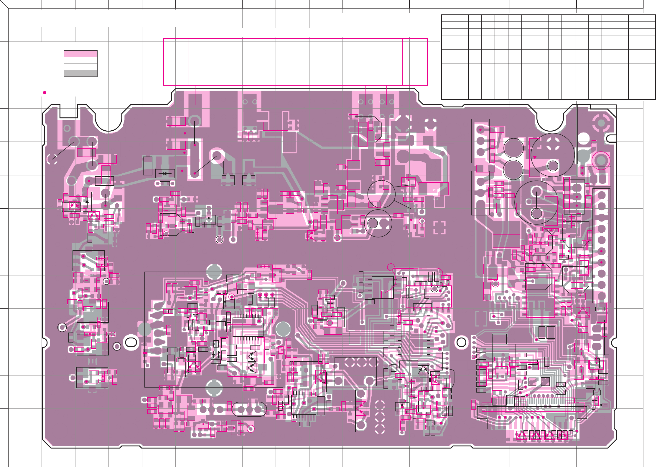
ABCD E F G H I J K L M N O P Q R S
1
2
3
4
5
6
7
8
9
10
11
12
13
14
C91
C67
D12
D13
R93
C104
Q32
L24
L20
L25
IC5
IC6
IC3
C10
C7
C3
C60
C107
C75
Q9
C54
XF1
CN4
CN5
C50
C131
C117
C161
C160
R68
C74
C46
C43
R44
IC4
R78
IC7
C103
C98
C81
R71
Q12
C89
C93
C99
C1
C5
C8
C11
C2
C6
C9
C12
C141
C144
C134
IC12
C39
C32
C203
C207
C210
C212
L18
C213
L15
C138
D33
C211
L13
L11
C86
C64
CF2
CF1
R87C96
C97
C16
C17
C18
C19 C21
C15
C14
C13
R9
R10
R11
R59
C72
Q2
R91
R37
R34
R56
R86
D9
C40
R53
R52
R51
C84
IC11
R8
R7
R2
R66 R49
R40
TH1
R5
R6
R177
R62
R57
C61
R1
R3
R4
C45
C70
R50
R75
C165
R131
C79
C80
R67
R63
R48
R89
R77
R90
R64
R70
Q11
R65
R79R82
R85
R27
L21
C198
C214
D34
L22
C171
C208
R76C83
IC13
C166
C172
C114
C195
C30
C35
C47
C63
L23
Q8
R188
Q37
R193
D40
L26
R202
R201
Q38
R197
L5
C261
C260
R195
Q39
C77
D25
R19
Q35
R208
TV
8R
CV
J72-0677-02 A/2
+
+
+
A1 : X58-4670-XX
8CL
+
+
1
1011
20
1
8 9
16
+
G
O
I
+
+
+
+
+
+
1
45
8
+
1
1213
24
+
+
+
G
DS
5C
G
SD
1
45
8
SB
GND
DEO
DTC
IGN
DI
ME
MI
PTT
SQ
1
8
RSSI
GND
E
C
B
O
G
I
GND
B
+
+
J1
EXT. SP
CN7
1
3
PA/LI
SPI
SPO
CN8 2
1
E
10 SP
+
+
CN3
SB
E
HOR
3
1
1
1
3
AM
MM
EMG/TXS
G
DS
CN1
15
1
GND
MIO
MII
AFI
AFO
ALT
AUX2
AUX4
AUX1
AUX3
NC
AUX6
AUX5
5S
8C
R155
R160
D22
C92
C94
C95
R69
L17
IC14
R123
R95
C200
C156
R133
Q23
C221
C205
C148
C222
C274
R170
D29
C179
D2
Q1
D24
C4
R29
R151
C142
C174
R108
R113
C139
C168
R137
C151
R121
C147
C170
D17
C162
C159
R101
R98 C112
C115
C118
C120
R106
R92
UL C125
R148
R146
R150
Q4
D3
D4
D5
R13
Q6
D14
Q17
C106
Q13
C88
D11
R43 C37
C66
R61
C69
D1
R22
C121
C119
C190
C157
C180
R115
Q29
R178
C123
R107
R136
Q24
C186
Q19
SP
C128
C116
C113 IC10
Q21
R175
C204
C196
C217
C223
R169
IC15
D36
D35
C224
C220
R157
C183
C187
R162
C177
R112
R110
C130
C133
C152
R166
Q33
Q16
C215
C219
C209
C127
C23
L10
C149
C169
C192
Q7
C41
C44
C52
R23
R46
D21
R138
R134 R126
D27
Q5
R103
R163
1
4 5
8
C102
IC8
Q3
R18
R58
R16
R30
R39
R24
F1
C143
R142
R100
R21
R14
R116
Q18
Q28
R159
R33
R25
C33
R36
L1
C36
C26
R31
C31
C181
Q25
L14
C158
L12
Q22
R127
R132
R144
C189
R128
R119
R109
R129
R111
C132
C137
R117
D16
R97
L6
R118
C135
C124
R94 C105
C110
Q
14
L9
C100
C82
L8
C126
R105
L7 R99
Q15
R88
R125
R145
Q26
R152
R122
R135
D20
R32
R38
C24
R17
R12 C20
R153
D19
D15
C129
C150
R83
R80 C87
R81
R149
R47
R72
R60
C78
C58
R54
R168
R139
R141
R130
R173
R174
R41
R20 R15
C29
R26
R120
Q20
R114
C153
C163
R154
R176
R179
R172
C154
C164
R124
R181
R180
R164
C216
R171
R167
Q27
R147
R161
C167
C175
C136
C155
C62 C56
L4 L2
L3
C49
D10
D8
C146
C230
C231
C241
R182
R183
R184
C122
C173
C185
C194
C201
C218
C22
C51
C53
D18
D23 TV
D28
D30
D31
IC2
Q10
Q31
X1
R186
C248
L33
D39
R189
R190
R192
L27
C259
R42
R35
R185
R196
PC
Q36
R194
R55
R210
C264
R140
ANT
G1
S
G2
D
G1
S
G2
D
RX
(ST)
HT
E
8CL
MD
CV
1
3 4
5
1 2 3 4
IC400
+
+
8RC
CK DT ST
B
C
E
B
C
E
E
8T
C
B
9C
1
34
5
+
+
8TC
IC9
1
8 9
16
ASQ
+
IC1
1
34
5
+
5C
O
G
I
+
+
B
E
C
+
1
78
14
CN2
1
34
E
MIO
MII
DEO
ALT
ME
MI
MM
8C
EMG/TXS
AUX2
AUX4
AUX1
AUX3
PSW
SB
SB
AFO
MO
DTMFIO
CTO
W/N
CNTCK
CNTDT
DAST
SPTST
TO
ASQ
RSSI
PLCK
PLDT
PLST
UL
SFTDT
C272 +
TK-760G/762G PC BOARD VIEW
61
TX-RX UNIT (X57-5950-XX) (A/2)
Component side view + Foil side
-10 : TK-760G K -11 : TK-762G K -12 : TK-760G K2 -13 : TK-762G K2 -21 : TK-760G M
Component side
Foil side
Pattern 1
Pattern 2
Pattern 3
Pattern 4
Connect 1 and 4
Ref. No. Address
IC1 11O
IC2 9J
IC3 10H
IC4 12M
IC5 12I
IC6 10M
IC7 9L
IC8 9F
IC9 9M
IC10 8O
IC11 10J
Ref. No. Address
IC12 6O
IC13 8R
IC14 9P
IC15 7E
IC400 2I
Q1 11R
Q2 12R
Q3 12L
Q4 12L
Q5 11R
Q6 11R
Ref. No. Address
Q7 11I
Q8 7G
Q9 10F
Q10 13M
Q11 11G
Q12 11G
Q13 13I
Q14 10F
Q15 13E
Q16 13G
Q17 9R
Ref. No. Address
Q18 13F
Q19 7Q
Q20 8Q
Q21 7Q
Q22 7H
Q23 7O
Q24 8R
Q25 6J
Q26 8Q
Q27 9C
Q28 7K
Ref. No. Address
Q29 7M
Q31 6L
Q32 4O
Q33 7F
Q35 12L
Q36 9I
Q37 11L
Q38 12R
Q39 9N
D1 13P
D2 12R
Ref. No. Address
D3 13Q
D4 13Q
D5 13P
D8 12J
D9 9G
D10 12K
D11 12M
D12 11H
D13 11H
D14 10L
D15 10R
Ref. No. Address
D16 11F
D17 7H
D18 12C
D19 8R
D20 8P
D21 7Q
D22 7J
D23 10C
D24 8P
D25 6L
D27 8P
Ref. No. Address
D28 10C
D29 5P
D30 8C
D31 8C
D33 6C
D34 5E
D35 7C
D36 6B
D39 8H
D40 11M
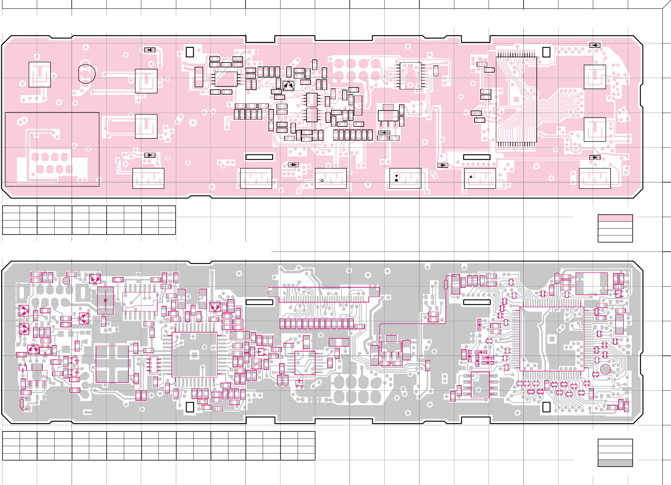
S
RQP
O
NMLK
J
IHGF
E
D
CB
A
1
2
3
4
5
6
7
8
9
10
11
12
13
14
F.RESET
SPD
X501
IC502
125
26
50
51 75
76
100
IC505
1
8
4
5
R508
R501
IC508
1
22
23
33
34 44
11
12
R583
Q504
Q508
IC509
1
7
8
14
C578
C584
D527
D524
D525
CP536
CP531
CP534
C559
C560
R575
CP538
CP530
R600
R599
D504
D501
D502
R595
R593
C590
C620
C615 C623
C504
C522 +
C553
Q
502
R548
R582
C555
+
C558
R578
C581
C587
C565
C566
R576
R614
R585
R613
CP517
R590
CP533 CP535
CP526
CP524
R607
C576
C577
CP532
CP522
CP529
CP521
CP518
CP523
CP520
C516
C518
C502
R511
R527
X502
R515
Q501
C514
R550
R554
C530
R553
C534
C549
C550
C533
R581
C557
C545
R610
R523 R509
CN501
L503
R617
R620
R621
CNT
CK
E
MBL 5C LCD
CS
SB CNT
DT
E
J72-0677-02 B/2
CP
519
IC511
1
78
14
CP514
CP513
R506
R507
R568
R530
C519
R584
C571 R586
IC512
O
G
I
C583
+
+
C575
D528
R598
R569 CP539
C547 C552
R565
R588
CP505
CP527
D508
C574
Q503
C572
L510
C633
C596
C594
C598
R608
C612
Q509
R605
C611
C582
C604
C608
C610
C606
C602
C600
C618
C621
C616
C597
C506
R513
C539
C568
+
+C564
C567
C540
C563
R571
R574
Q506
C589
R591
C569
C573
R579
C551
R577
R587
R615
R606
R612
Q505
B
C
E
R594
R516
C556
D523
CP516
C579
C515
R528
C585
R604
R580
C546
CP501
R603
CP502
CP510
CP509
CP508
CP503
CP512
CP511
CP504
D503
R558
C536
R546
R549
C535
C548
R557
C562
R573
C554
R570
C544
C561
R611
R522
C509
R701
+
R503
R502
R504
1
34
L504
C570
C629
C720 +
D505
D507
D526
E
MIO
MII
DEO
ALT
ME
MI
MM
8C
EMG/TXS
AUX2
AUX4
AUX1
AUX3
PSW
SB
SB
AFO
MO
DTMFIO
CTO
W/N
CNTCK
CNTDT
DAST
SPTST
TO
ASQ
RSSI
PLCK
PLDT
PLST
UL
SFTDT
R529
R538
C521
R555
R592
R519
C508
R514
R572
D521
R602
C603
C609
C605
C601
C599
C613
C503
IC503
G
I
O
C507
R526
R536
C524
R556
C526
C626
C628
R616
R539
C580
R531
C523
C538
+
R534
R518
R510
R532
R537
C520
R551
C532
R540
R541
C630 +
C631
D529
R622
IC501
1
16
17
32
IC510
1
CNT
CK
89
16
C501
R505
IC507
1
45
8
C543
R560
R562C541R563
R564
R561
C542
C537
D514
A (TK-760G)
MON (TK-762G)
D/A (TK-760G)
(TK-762G)
(TK-760G)
(TK-762G)
(TK-760G)
A (TK-762G)
SCN
(TK-760G)
CH
DN
CH
UP
C517
E
MBL 5C LCD
CS
SB CNT
DT
E
D511
C505
R544
C528
C531
C527
R566
R559R567
J501
MBLGNDME
HOOK/
RXD
CM MIC PTT/
TXD PSB
D513
MON
(TK-760G)
J72-0677-02 B/2 D512
PSW
VOL
UP
VOL
DN
D509
R533
D510
R542
R512
D506
R535
C525
R545
R543
R547
C529 R552
R520
R521
L501
R517
R618
R619
IC513
IC514
1
45
8
1
45
8
Component side
Foil side
Pattern 1
Pattern 2
Pattern 3
Pattern 4
PC BOARD VIEWS TK-760G/762G
Ref. No.
Address
D506 4L
D509 5M
D510 5R
Ref. No.
Address
IC501 3O
IC503 4L
IC507 3G
Ref. No.
Address
IC510 2L
IC513 3I
IC514 4I
Ref. No.
Address
D511 2R
D512 2E
D513 5E
Ref. No.
Address
D514 5I
D521 2C
D529 3I
TX-RX UNIT (X57-5950-XX) (B/2) Component side view
-10 : TK-760G K -11 : TK-762G K -12 : TK-760G K2 -13 : TK-762G K2 -21 : TK-760G M
TX-RX UNIT (X57-5950-XX) (B/2) Foil side view
-10 : TK-760G K -11 : TK-762G K -12 : TK-760G K2 -13 : TK-762G K2 -21 : TK-760G M
64
Component side
Foil side
Pattern 1
Pattern 2
Pattern 3
Pattern 4
63
Ref. No.
Address
IC502 10P
IC505 11N
IC508 10F
Ref. No.
Address
IC509 11I
IC511 9D
IC512 10L
Ref. No.
Address
Q501 9R
Q502 10H
Q503 11I
Ref. No.
Address
Q504 11C
Q505 11B
Q506 11A
Ref. No.
Address
Q508 11C
Q509 10B
D501 11N
Ref. No.
Address
D502 10N
D503 10N
D504 11N
Ref. No.
Address
D505 11N
D507 10N
D508 9G
Ref. No.
Address
D523 10A
D524 9A
D525 9C
Ref. No.
Address
D526 9C
D527 10A
D528 8C
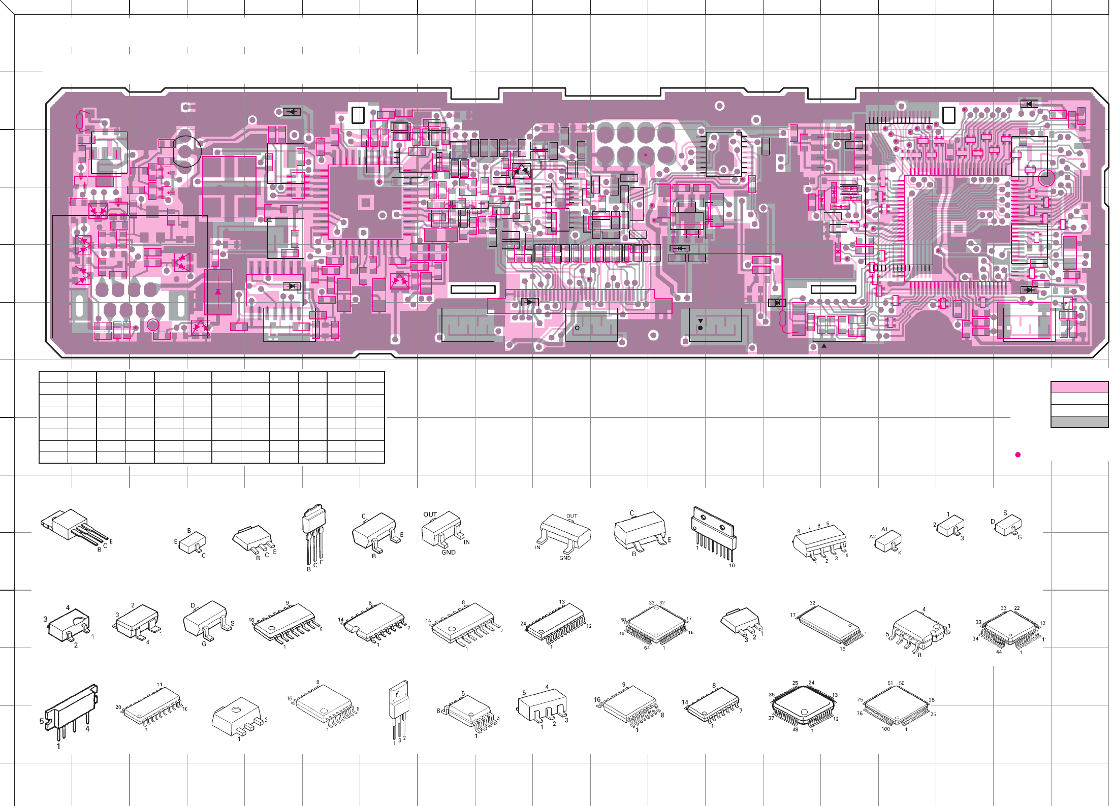
ABCD E F G H I J K L M N O P Q R S
1
2
3
4
5
6
7
8
9
10
11
12
13
14
R529
R538 C521
R555
R592
R519 C508
R514
R572
D521
R602
C603
C609
C605
C601
C599
C613
C503
IC503
G
I
O
C507
R526
R536
C524
R556
C526
C626
C628
R616
R539
C580
R531
C523
C538
+
R534
R518
R510
R532
R537
C520
R551
C532
R540
R541
C630 +
C631
D529
R622
IC501
1
16
17
32
IC510
1
CNT
CK
8 9
16 C501
R505
IC507
1
4 5
8
C543
R560
R562
C541
R563
R564
R561
C542
C537
D514
CH
DN
CH
UP
C517
E
MBL 5C LCD
CS
SB CNT
DT
E
D511
C505
R544
C528
C531
C527
R566 R559
R567
J501
PSW
MBLGNDME
HOOK/
RXD
CM MIC PTT/
TXD PSB D513
J72-0677-02 B/2 D512
VOL
UP
VOL
DN
D509
R533
D510
R542
R512 D506
R535
C525
R545
R543
R547
C529 R552
R520
R521
L501
R517
R618
R619
IC513
IC514
1
45
8
1
45
8
MON
(TK-760G)
A (TK-760G)
MON (TK-762G) D/A (TK-760G)
(TK-762G) (TK-760G)
(TK-762G)
(TK-760G)
A (TK-762G)
SCN
(TK-760G)
F.RESET
SPD
X501
IC502
125
26
5051 7576
100
IC505
18
45
R508
R501
IC508
1
22
23
33
34 44
11
12
R583
Q504
Q508
IC509 1
78
14
C578
C584
D527
D524
D525
CP536
CP531
CP534
C559
C560
R575
CP538
CP530
R600
R599
D504
D501
D502
R595
R593
C590
C620
C615
C623
C504
C522 +
C553
R548
Q
502
R582
C555
+
C558
R578
C581
C587
C565
C566
R576
R614
R585
R613
CP
519
CP517
R590 CP533
CP535
CP526
CP524
R607
C576
C577
CP532
CP522
CP529
CP521
CP518
CP523
CP520
C516
C518
C502
R511
R527 X502
R515
Q501
C514
R550
R554
C530
R553
C534
C549
C550
C533
R581
C557
C545
R610
R523 R509
CN501
L503
R617
R620
R621
IC511
1
78
14
CP514
CP513
R506
R507
R568
R530
C519
R584
C571
R586
IC512 O
G
I
C583 +
+
C575
D528
R598
R569
CP539
C547
C552
R565
R588
CP505
CP527
D508
C574
Q503
C572
L510
C633
C596 C594
C598
R608
C612 Q509
R605
C611
C582
C604
C608 C610
C606
C602
C600
C618
C621
C616
C597
C506
R513
C539
C568 +
+
C564
C567
C540
C563
R571
R574
Q506
C589
R591
C569
C573
R579
C551
R577
R587
R615
R606
R612
Q505
B
C
E
R594
R516
C556
D523
CP516
C579
C515
R528
C585
R604
R580
C546
CP501
R603
CP502 CP510
CP509
CP508
CP503
CP512
CP511
CP504
D503
R558
C536
R546
R549
C535
C548
R557
C562
R573
C554
R570
C544
C561
R611
R522
C509
R701
+
R503
R502
R504
1
34
E
MIO
MII
DEO
ALT
ME
MI
MM
8C
EMG/TXS
AUX2
AUX4
AUX1
AUX3
PSW
SB
SB
AFO
MO
DTMFIO
CTO
W/N
CNTCK
CNTDT
DAST
SPTST
TO
ASQ
RSSI
PLCK
PLDT
PLST
UL
SFTDT
L504
C570
C629
C720
+
D505
D507
D526
TK-760G/762G PC BOARD VIEW
65 66
TX-RX UNIT (X57-5950-XX) (B/2) Component side view + Foil side
-10 : TK-760G K -11 : TK-762G K -12 : TK-760G K2 -13 : TK-762G K2 -21 : TK-760G M
Component side
Foil side
Pattern 1
Pattern 2
Pattern 3
Pattern 4
Connect 1 and 4
Ref. No. Address
IC501 4P
IC502 4Q
IC503 4L
IC505 3O
IC507 3H
IC508 4G
IC509 3J
Ref. No. Address
IC510 3M
IC511 5E
IC512 4L
IC513 4J
IC514 4J
Q501 5S
Q502 4I
Ref. No. Address
Q503 3J
Q504 3C
Q505 3B
Q506 3B
Q508 4C
Q509 4B
D501 4O
Ref. No. Address
D502 4O
D503 5O
D504 4O
D505 4O
D506 5L
D507 4O
D508 5G
Ref. No. Address
D509 5N
D510 5R
D511 2R
D512 2E
D513 5E
D514 5I
D521 3C
Ref. No. Address
D523 4B
D524 5B
D525 5C
D526 5D
D527 4B
D528 6D
D529 3I
2SB1565 DTC114EE
2SA1745
2SA1832
2SC2412K
2SC4215
2SC4226
2SB1132
2SC2954
2SC3357
2SA1641 2SC4081 DTC363EU DTA114EKA
DTC114EKA
DTC114EUA
DTC144EKA
DTD114EK
KRA225S
2SC4649 LA4422 NJM2904M
NJM4558M
TA75W558FU
TC75W51FU
DAN202K
DAN202U
DAN235K
MA742 2SK508NV
3SK241 3SK228 2SK1824 BU4094BCF TC4013BF BU4066BCFV M62363FP LC75823W AN8009M AT29C020-90TI AT2408N10SI2.5 TC35453F
M67741H-32
M67741L-35 MB15A02 NJM78L05UA
RH5VL42C
S-81350HG-KD
BU4094BCFV TA7808S NJM2904V
UPB1509GVTA75S01F TA31136FN LC73872M LC75833W
2SC4617
2SC4619
2SC4738
30622M4102GP
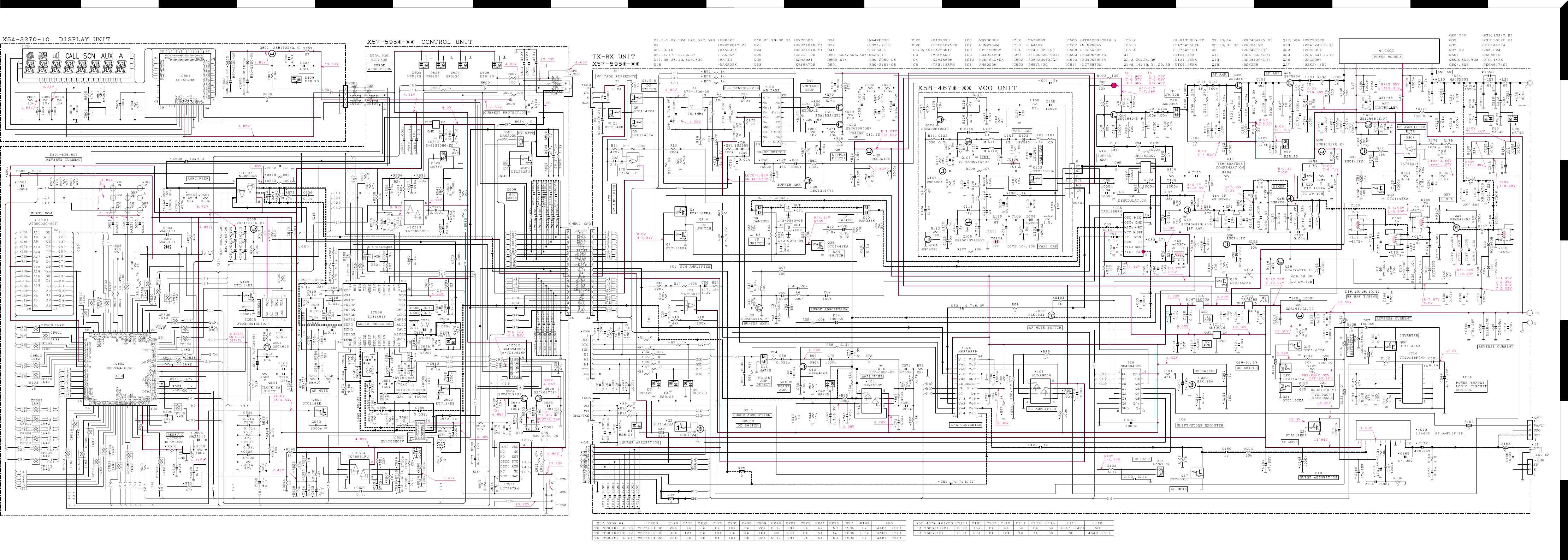
TRPNLJHFDB SQ
OMKIGECA
1
3
5
7
2
4
6
SCHEMATIC DIAGRAM TK-760G
Note : Components marked with a dot (·) are parts of patterun 1.
70
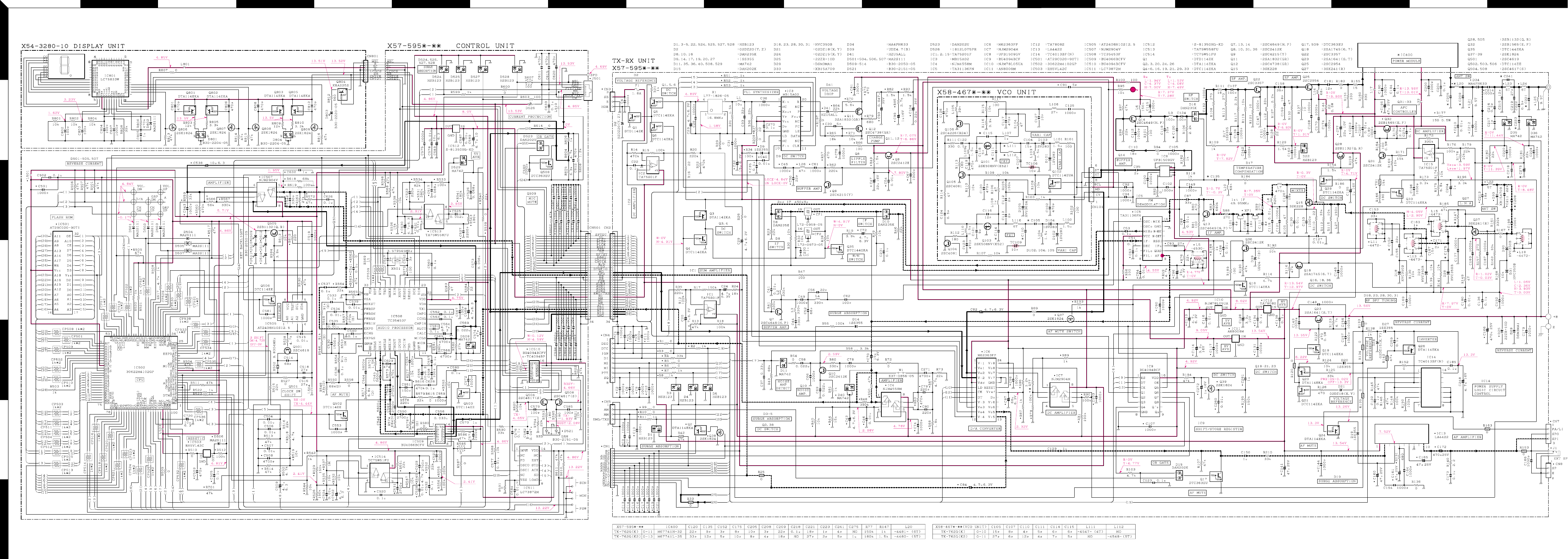
ACEGI KMOQS
BDF H J L N P R T
1
3
5
7
2
4
6
TK-762G SCHEMATIC DIAGRAM
71
Note : Components marked with a dot (·) are parts of patterun 1.
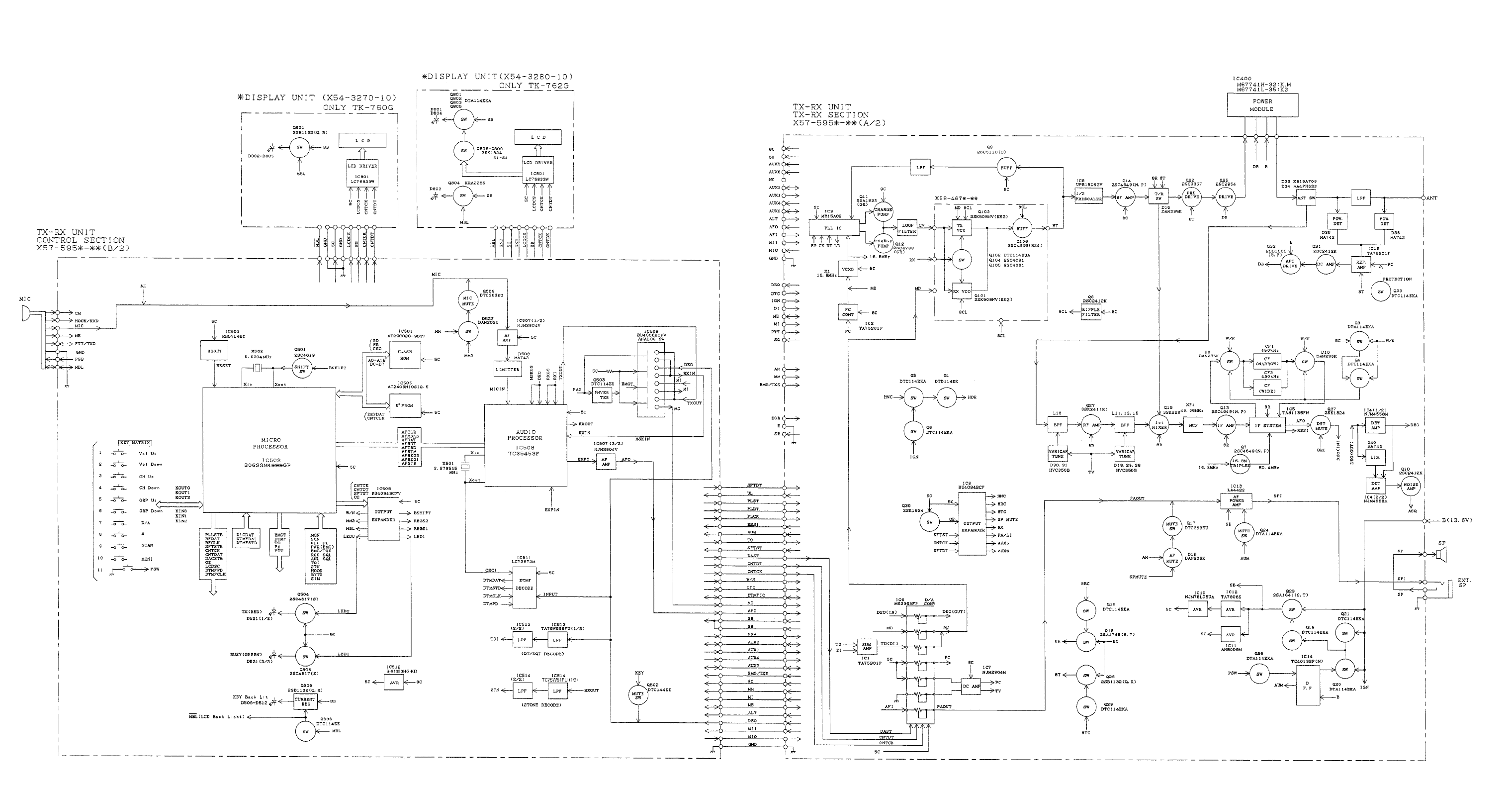
TK-760G/762G TK-760G/762G TK-760G/762G
BLOCK DIAGRAM
77
7978
LEVEL DIAGRAM
Receiver Section
Center Frequency 49.95MHz 450kHz Audio Frequency
Control Unit TX-RX Unit VCO Unit TX-RX Unit Power Module TX-RX Unit
To make measurements in the RF section, connect the RF
level meter.
In the RF section, use a 0.01µF coupling capacitor.
(The display shows the SSG input value required to obtain
12dB SINAD.)
To make measurements in the AF section, connect the AC level meter.
(ANT input : –53dBm, 1kHz FM, 3kHz DEV (Wide) / 1.5kHz DEV (Narrow))
The AF output level is adjusted for 0.45V/4Ω by the front panel AF VOL control.
To make measurements in
the RF section, connect the
RF wattmeter (50Ω).
To make measurements in the AF section, connect the AC level meter.
AG is set so that MIC input becomes 3kHz/1.5kHz (Wide/Narrow) DEV at 1kHz MOD.
Transmitter Section
TK-760G/762GTK-760G/762G
80
TK-760G/762G
TERMINAL FUNCTION
CN1 (TX-RX Unit)
Pin No.
Name Function
1 8C DC 8V output.
2 5S DC 5V output.
3 AUX5 SMRD : Reset output. *1
4 AUX6 5SC : 5S control (Cannot use). *1
5 NC Non-connection
6 AUX3 SMCK : Clock pulse output. *1
SQ : Squelch detect output. *2
7 AUX1 SMRQ : Ack Req input. *1
PTT : External PTT input. *2
8 AUX4 TXD : Serial control data output. *1
9 AUX2 RXD : Serial control data input. *1
DTC : Data channel control/External hook input.
CHDATA : Channel control serial data input.
10 ALT Alert tone input.
11 AFO Receiver audio signal output.
12 AFI Reseiver audio signal input.
13 MII Transmit audio signal input.
14 MIO Transmit audio signal output.
15 GND Ground
.
CN2 (TX-RX Unit) ←→ CN501 (Control Unit)
Pin No.
Name Function
1 SFTDT Serial data for IC9 (Shift register).
2 UL Lock detect.
3 PLST Strobe signal for IC3 (PLL IC).
4 PLDT Serial data for IC3 (PLL IC).
5 PLCK Clock pulse for IC3 (PLL IC).
6 RSSI Receive signal strength indicator.
7 ASQ Analog squelch.
8 TO Transmit sub-tone signal output.
9 SFTST Strobe signal for IC9 (Shift register).
10 DAST Strobe signal for IC6 (Shift register).
11 CNTDT Control serial data for IC6.
12 CNTCK Control clock pulse for IC6.
13 W/N Change signal of wide or narrow.
14 CTO Received sub-tone signal.
15 DTMFIO DTMF signal.
16 MO Modulation signal.
17 AFO Receiver audio signal.
18 SB Switched B.
19 SB Switched B.
20 PSW Power switch.
21 AUX3 Optional unit control signal.
22 AUX1 Optional unit control signal.
23 AUX4 Optional unit control singal.
24 AUX2 Optional unit control signal.
25 EMG/TXS Foot switch input signal.
26 8C DC 8V.
27 MM MIC mute.
28 MI External MIC input signal.
29 ME MIC ground.
30 ALT Alert tone signal.
31 DEO Receiver detector output.
32 MII Transmit audio signal input.
33 MIO Transmit audio signal output.
34 GND Grond.
CN3 (TX-RX Unit)
Pin No.
Name Function
1 HOR Horn alert/call output.
2 E Ground.
3SB
Switched B+, DC 13.6V output, Maximum 1A.
CN4 (TX-RX Unit)
Pin No.
Name Function
1 DEO Receiver detector output.
Level : 0.5Vrms (Atandard modulation)
2 DTC Data channel control/External hook input.
3 IGN Ignition sense input.
4 DI Data modulation input.
5 ME External microphone ground.
6 MI EXternal microphone input.
7 PTT External PTT input, active low.
8 SQ Squelch detect output.
CN5 (TX-RX Unit)
Pin No.
Name Function
1 AM Speaker mute input, active high.
2 MM MIC mute input, active high
3 EMG/TXS EMG : Foot switch input, active low. *3
CN7 (TX-RX Unit)
Pin No.
Name Function
1 PA/LI Relay for PA function KAP-1 control.
“H” : PA/LI on, “L” : PA/LI off
2 SPO Audio signal output to KAP-1
3 SPI Audio signal inpt from KAP-1
CN8 (TX-RX Unit)
Pin No.
Name Function
1SP
Audio signal output to internal/external speaker.
2 E Ground
J501 (Control Unit)
Pin No.
Name Function
1 MBL MIC backlight control.
2 PSB 13.6V.
3 GND Ground.
4 PTT/TXD PTT.
5 ME MIC ground.
6 MIC MIC signal input.
7 HOOK/RXD Hook detection
8 CM MIC data detection.
CN101 (PLL/VCO) ←→ TX-RX Unit
Pin No.
Name Function
1 CV Control voltage input.
2 MD Modulation input.
3 8CL 8V input.
4 E Ground.
5 HT Signal output.
6 RX (ST) Switched transmit input. H : Transmit
*1 : SmarTrunk OMNI mode
*2 : MDT mode
*3 : Emergency mode
81
TK-760G/762G
SPECIFICATIONS
GENERAL
Frequency Range ................................ K : 148 to 174MHz K2 : 136 to 162MHz M : 146 to 174MHz
Number of Channels ........................... TK-762G : Maximum 8 channels TK-760G : Maximum 128 channels
Number of Groups .............................. TK-760G : Maximum 128 groups
Channel Spacing ................................. Wide : 25, 30kHz Narrow : 12.5, 15kHz
PLL Channel Stepping ........................ 2.5, 3.75, 5, 6.25, 7.5kHz
Operating Voltage ............................... 13.6V DC ±15%
Current Drain ...................................... Less than 0.4A on standby
Less than 1.0A on receive
Less than 8.0A on transmit
Operating Temperature Range ........... –30°C to +60°C (–22°F to +140°F)
Dimensions & Weight ........................ 140 (5-33/64) W x 40 (1-37/64) H x 145 (5-45/64) D mm (inch), 940g (2.07 lbs)
Channel Frequency Spread ................ K : 26MHz M : 28MHz
RECEIVER (Measurements made per EIA standard EIA/TIA-204-D)
Sensitivity (12dB SINAD) .................... Wide : 0.25µV Narrow : 0.33µV
Selectivity ........................................... Wide : 85dB Narrow : 75dB
Intermodulation................................... Wide : 75dB Narrow : 65dB
Spurious Responce ............................. 90dB
Audio Power Output ........................... 4.0W
Frequency Stability ............................. ±2.5ppm
TRANSMITTER (Measurements made per EIA standard EIA-152-C)
RF Power Output ................................ 25W
Spurious and Harmonics..................... 70dB
Modulation .......................................... Wide : 16K0F3E Narrow : 11K0F3E
FM Noise ............................................ Wide : 50dB Narrow : 45dB
Audio Distortion .................................. Less than 3%
Frequency Stability ............................. ±2.5ppm
KENWOOD CORPORATION
14-6, Dogenzaka 1-chome, Shibuya-ku, Tokyo 150-8501, Japan
KENWOOD SERVICE CORPORATION
P.O. BOX 22745, 2201 East Dominguez Street, Long Beach, CA 90801-5745, U.S.A.
KENWOOD ELECTRONICS CANADA INC.
6070 Kestrel Road, Mississauga, Ontario, Canada L5T 1S8
KENWOOD ELECTRONICS DEUTSCHLAND GMBH
Rembrücker Str. 15, 63150 Heusenstamm, Germany
KENWOOD ELECTRONICS BELGIUM N.V.
Mechelsesteenweg 418 B-1930 Zaventem, Belgium
KENWOOD ELECTRONICS FRANCE S.A.
13, Boulevard Ney, 75018 Paris, France
KENWOOD ELECTRONICS U.K. LIMITED
KENWOOD House, Dwight Road, Watford, Herts., WD1 8EB United Kingdom
KENWOOD ELECTRONICS EUROPE B.V.
Amsterdamseweg 37, 1422 AC Uithoorn, The Netherlands
KENWOOD ELECTRONICS ITALIA S.p.A.
Via G. Sirtori, 7/9 20129 Milano, Italy
KENWOOD IBERICA S.A.
Bolivia, 239-08020 Barcelona, Spain
KENWOOD ELECTRONICS AUSTRALIA PTY. LTD.
(A.C.N. 001 499 074)
16 Giffnock Avenue, Centrecourt Estate, North Ryde, N.S.W. 2113 Australia
KENWOOD ELECTRONICS (HONG KONG) LTD.
Unit 3712-3724, Level 37, Tower one Metroplaza, 223 Hing Fong Road, Kwai Fong, N.T., Hong Kong
KENWOOD ELECTRONICS TECHNOLOGIES(S) PTE LTD.
Sales Marketing Division
1 Ang Mo Kio Street 63, Singapore 569110
TK-760G/762G
