User manual

Version 1.0
Reproduction forbidden without Kyocera Corporation written authorization - All Rights Reserved
- 1 -
KA36 Hardware User Guide

Version 1.0
Reproduction forbidden without Kyocera Corporation written authorization - All Rights Reserved
- 2 -
Document History
Change Details
Revision
Date Chapter
Section Description
1.0 2015/7/7 - - First edition

Version 1.0
Reproduction forbidden without Kyocera Corporation written authorization - All Rights Reserved
- 3 -
Contents
1.
Scope
................................
................................................................
................................................................
................................................................
........................................................
................................................
........................
4
44
4
2.
Environmental condition
................................
................................................................
................................................................
................................................................
.....................................
..........
.....
4
44
4
3.
Electrical specifications
................................
................................................................
................................................................
................................................................
......................................
............
......
4
44
4
3.1
Absolute maximum ratings ........................................................................................................................... 4
3.2
Recommend operating condition ................................................................................................................. 5
3.3
Radio Specifications ....................................................................................................................................... 5
3.3.1
Cellular Specifications ................................................................................................................................ 5
3.3.2
GPS Receiver Specifications ...................................................................................................................... 5
4
Interface Descriptions
................................
................................................................
................................................................
................................................................
.......................................
..............
.......
6
66
6
4.1
Pad Assignment .............................................................................................................................................. 6
5
Input output signal specifications
................................
................................................................
............................................................
........................................................
............................
7
77
7
5.1
Antenna Port ................................................................................................................................................... 7
5.1.1
Main antenna port ...................................................................................................................................... 7
5.1.2
Second antenna port ................................................................................................................................. 7
5.1.3
GPS antenna port ....................................................................................................................................... 7
5.2
Pad Description ............................................................................................................................................... 8
6.
Module Control ................................................................................................................................................. 9
6.1
Power off and reset limitations .................................................................................................................... 9
6.2
Power supply interrupt .................................................................................................................................. 9
6.3
Over-temperature Protection ....................................................................................................................... 9
6.4
Over-temperature Protection (restricted RF operation). .......................................................................... 9
7.
UART/USB
................................
................................................................
................................................................
................................................................
..................................................
....................................
..................
10
1010
10
7.1
UART .............................................................................................................................................................. 10
7.1.1
UART2 ........................................................................................................................................................ 10
7.1.2
RI ................................................................................................................................................................ 10
7.2
USB ................................................................................................................................................................ 10
8.
Mechanical Information
................................
................................................................
................................................................
................................................................
.....................................
..........
.....
11
1111
11
9.
Mechanical Drawings
................................
................................................................
................................................................
................................................................
........................................
................
........
11
1111
11
10.
Related Documents
................................
................................................................
................................................................
................................................................
.......................................
..............
.......
12
1212
12
11.
Warnings
................................
................................................................
................................................................
................................................................
.................................................
..................................
.................
12
1212
12
11.1
Handling Precautions ............................................................................................................................... 12
12.
FCC/IC Regulatory notices
................................
................................................................
................................................................
................................................................
................................
13
1313
13
12.1
Modification statement ............................................................................................................................ 13
12.2
Interference statement ........................................................................................................................... 13
12.3
RF Exposure Information ........................................................................................................................ 13
12.4
IC Regulations ........................................................................................................................................... 14
12.5
FCC Class B digital device notice ........................................................................................................... 15
Version 1.0
Reproduction forbidden without Kyocera Corporation written authorization - All Rights Reserved
- 4 -
1.
Scope
This document is applied to wireless module of KA36 for North America.
2.
Environmental condition
(1)Withstand voltage :MAINVCC 5.0V (Not be destructed)
:USBV 7.0V (Not be destructed)
3.
Electrical specifications
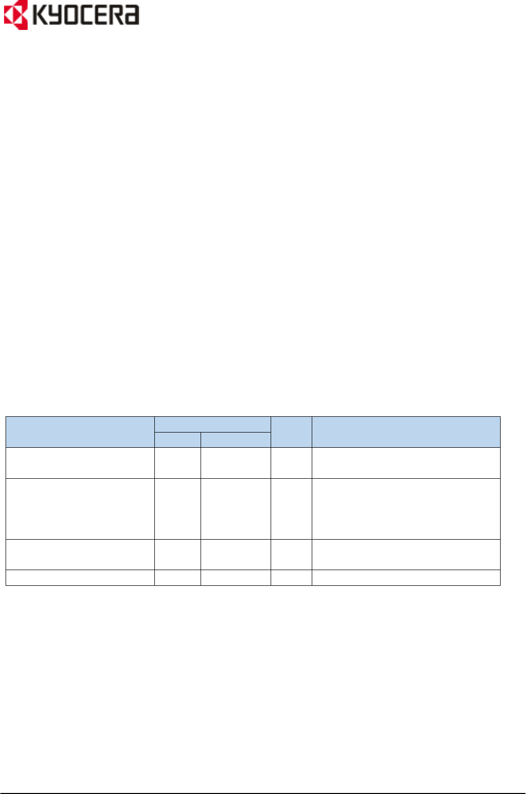
3.1 Absolute maximum ratings
Table3-1. Absolute maximum ratings
Parameter Rating Units
Note
Min Max
MAINVCC withstand voltage -0.3 5.0 V Applicable within the Operating temper-
ature
USBV withstand voltage -0.3 7.0 V Applicable within the Operating
temperature
Do not supply votage to USB+/USB-
pin when USBV is absent.
Digital interface input voltage -0.3 V
IOVCC
+0.3 V Applicable within the Operating
temperature
Storage Temperature -40 +85 ℃ Tstg

Version 1.0
Reproduction forbidden without Kyocera Corporation written authorization - All Rights Reserved
- 5 -
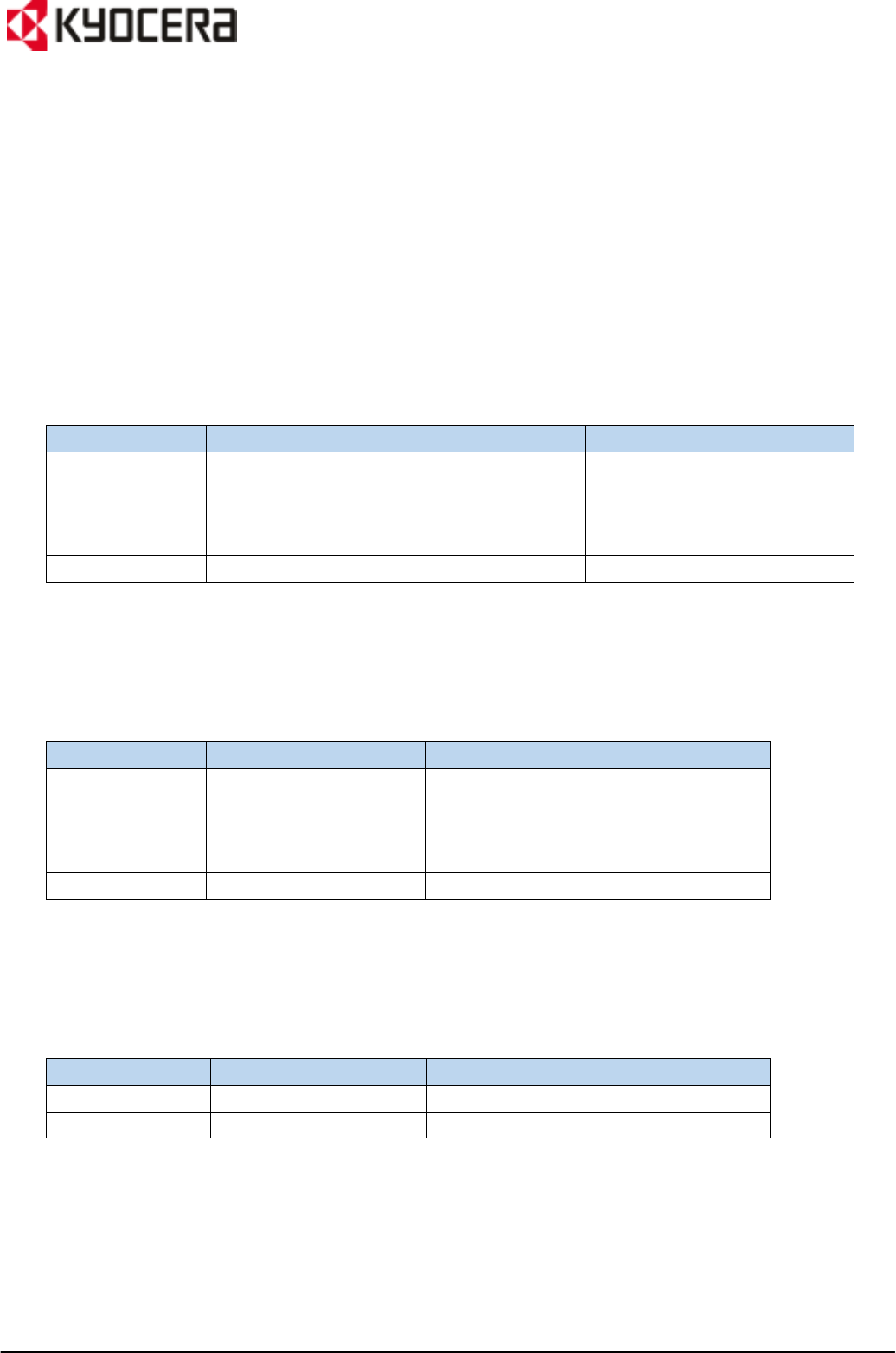
3.2 Recommend operating condition
Table3-2. Recommend operating condition
Parameter Rating Unit Note
Min Max
Operation voltage 3.6 4.2 V Applicable within the Operating temperature
includes momentary fluctuations such as ripple
and under/over shoot.
USBV input 4.5 5.25 V Applicable within the Operating temperature
3.3 Radio Specifications
3.3.1 Cellular Specifications
Unless otherwise specified, values in tables below are determined defined in performance tempera-
ture range.
<UMTS/HSPA+>
Frequency band: B2/B5
Output Power : Power Class 3
Also, the transmitter/receiver performance conform to 3GPP TS 34.121.
<LTE>
Frequency band: B2/B4/B5/B12
Output Power : Power Class 3
Categry : 3
Also, the transmitter/receiver performance conform to 3GPP TS36.101, TS36.521-1.
3.3.2 GPS Receiver Specifications
Unless otherwise specified, values in tables below are determined defined in performance tempera-
ture range.
Table3-4-2. GPS Receiver Specifications
Item Rating Note
Receiver sensitivity
(Sensitivity of capture)
-145 dBm or less Receiver sensitivity is defined by the input
power when the device can acquire the
satellite at a rate of 60%.
Receiver sensitivity
(Tracking Sensitivity)
-152 dBm or less Receiver sensitivity is defined by the input
power when the device can acquire the
satellite at a rate of 60%.

Version 1.0
Reproduction forbidden without Kyocera Corporation written authorization - All Rights Reserved
- 6 -
4
Interface Descriptions
4.1 Pad Assignment
Figure 4-1-4 shows Pad assignments.
Figure 4-1-4 (Bottom View)Pad assignments
Version 1.0
Reproduction forbidden without Kyocera Corporation written authorization - All Rights Reserved
- 7 -
5
Input output signal specifications
5.1 Antenna Port
The module has main antenna for transmission and reception, second antenna for reception
and GPS antenna in the interface.
Shows antenna port Specification.
5.1.1 Main antenna port
Table5-1-1 Main antenna characteristic
Characteristic Value Remarks
Frequency range B2: TX 1850-1910MHz / RX 1930-1990MHz
B4: TX 1710-1755MHz / RX 2110-2155MHz
B5: TX 824-849MHz / RX 869-894MHz
B12: TX 699-716MHz / RX 729-746MHz
Impedance 50Ω Nominal value
5.1.2 Second antenna port
Table5-1-2 Second antenna characteristic
Characteristic Value Remarks
Frequency range B2: RX 1930-1990MHz
B4: RX 2110-2155MHz
B5: RX 869-894MHz
B12: RX 729-746MHz
Impedance 50Ω Nominal value
5.1.3 GPS antenna port
Table5-1-3 GPS antenna port characteristic
Characteristic Value Remarks
Frequency Range 1575.42±2MHz
Impedance 50Ω Nominal value
Version 1.0
Reproduction forbidden without Kyocera Corporation written authorization - All Rights Reserved
- 8 -
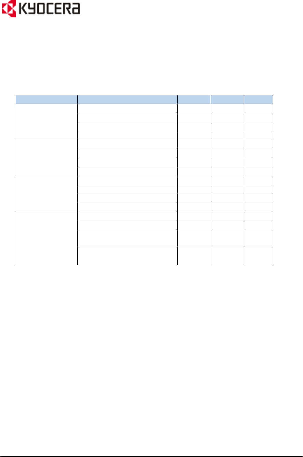
5.2 Pad Description
The table below shows the Logic characteristics for the digital IO’s under operation voltage and
operation temperature.
Table 5-2 PAD Description
IO voltage Parameter Min. Max. Unit
1.8V digital input High-level input voltage(VIH) 1.2 2.1 V
Low-level input voltage(VIL) -0.3 0.6 V
Pull up/down resistance(RPA) 55 391 kΩ
Pull up/down resistance(RPB) 10 101 kΩ
1.8V digital output High-level output voltage(VOH) 1.3 1.9 V
Low-level output voltage(VOL) 0 0.5 V
Output high drive strength - 2.0 mA
Output low drive strength -2.0 - mA
USB signal
(full-speed)
※
High-level input voltage(VIH) 1.27 - V
Low-level input voltage(VIL) - 0.85 V
High-level output voltage(VOH) 2.8 3.6 V
Low-level output voltage(VOL) - 0.3 V
RESETX signal High-level input voltage(VIH) 1.2 2.1 V
Low-level input voltage(VIL) -0.3 0.6 V
Input high leakage current with
pull-down(IIHPD)
- 35 uA
Input low leakage current with
pull-up(IILPU)
-200 - uA
※
USB High-speed is conforming to Universal Serial Bus Specification, rev. 2.0 (April 27, 2000 or later).
※
1.8V digital input (RPB) is applied for UIM_RST/UIM_CLK/UIM_DATA.
※
2.85V digital interface signals (UIM_RST/UIM_CLK/UIM_DATA) are conforming to ISO/IEC7816-3 CLASS B specifica-
tion.
※
VIH/VIL and VOH/VOL for 1.8V digital input/output signal are specified under IOVCC=1.8V.
※
VOH/VOL is specified at IOH=1mA/IOL=-1mA for 1.8V Digital output signal.

Version 1.0
Reproduction forbidden without Kyocera Corporation written authorization - All Rights Reserved
- 9 -
6. Module Control
6.1 Power off and reset limitations
There is no limitations to power off and reset.
6.2 Power supply interrupt
If MAINVCC drops out of range(<3.05V 1usec typ) then the module is completely shut down.
In thie case, please execute power-on sequence.
6.3 Over-temperature Protection
PM8018 provides over-temperature protection. If PM8018 die temperature greater than 150 °C,
the module is completely shut down.
Temperature hysteresis is incorporated such that the die
temperature must cool significantly (<110°C typ) before the module can be powered on again.
When the module bocome under 110°C(typ) and a PWR_N signal is enabled, the module will
power up.
Please execute power-on sequence.
6.4 Over-temperature Protection (restricted RF operation).
The thermistor built into the module (around Power Amplifier) detects the temperature around it.
Based on the detected limited temperature, the module starts or terminates temperature protec-
tion and stop transmit/receive functions to prevent devices to be destructed.
Version 1.0
Reproduction forbidden without Kyocera Corporation written authorization - All Rights Reserved
- 10 -
7. UART/USB
The module has USB and UART2 interface.
7.1 UART
The module has a UART interface.
7.1.1 UART2
UART2 function can be enabled/disabled by CONT1.
(CONT1=Open(High)→UART2 disabled, CONT1=Low→UART2 enabled)
Communication speed : 115,200 bps
Hard flow control : No
Parity bit : No
Start bit : 1
Stop bit : 1
Data bit : 8
Table7-1-1 UART2
Signal name I/O Outline
C-UART Up I Module receiving data
C-UART Dwn O Module sending data
CONT1 I UART2 enabled/disabled control
7.1.2 RI
The module has RI in the interface. RI is used to Ring indication (Incoming call).
Table7-1-2 RI
Signal name I/O Outline
RI O Ring (Incoming call) indication
7.2 USB
The module has USB 2.0 interface. USB 2.0 operates at 480Mbps called high speed.
USBV terminal controls USB operation such as operating/non-operating.
Table7-2 USB
Signal name I/O Outline
USBV I Power supply for USB
USB+ Both positive USB positive signal
USB- Both negative USB negative signal
Version 1.0
Reproduction forbidden without Kyocera Corporation written authorization - All Rights Reserved
- 11 -
8.
Mechanical Information
Table8. Mechanical Information
Parameter Specifications Definition
Dimensions approx. 40×40×4.3
Flatness 0.1mm or less
Weight approx. 11g
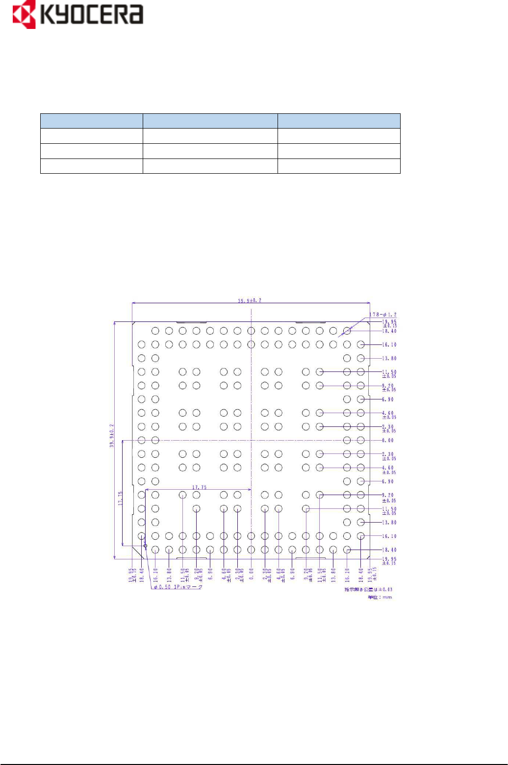
9.
Mechanical Drawings
Figure. 9-1 Bottom view with dimensions

Version 1.0
Reproduction forbidden without Kyocera Corporation written authorization - All Rights Reserved
- 12 -
10.
Related Documents
Product Specifications
AT Commands Function Specifications
11.
Warnings
11.1 Handling Precautions
The product is neither intended nor warranted for use in equipment or systems that require a
malfunction or failure of which may cause loss of human life, bodily injury.
1) Take care of static electricity when handling the product. Failure to do so may cause malfunction.
2) Do not expose the product to strong impacts such as by dropping.
Do not expose the product to wet.
Do not use the product under stresses beyond absolute maximum ratings, operating voltage and
operating temperature.
It is not the scope of our guarantee and repairs for unsatisfactory results due to installation
structure, misuse or inadequate usage of products in the catalog.
Do not disassembly, modifications or repairs. Doing so may cause the product to rupture, catch
fire, generate-heat or electric shock.
Disassembly or modifications constitutes a violation of the
Radio Act.
3) Storage temp: 25±10°C, Storage humidity: 60%RH, Storage period: 3 months or less at a dry
packaging.
After opening, you should mount the products while keeping them on the condition of 5 to
25±10°C and 60%RH or less in humidity within 7 days.
4) When the above-mentioned storage method could not be executed, please process the baking
treatment before mounting the products.
Recommended condition: 90℃ +8/-0℃ , ≦5% RH , 33 hours
5) The module is classified as MSL3.

Version 1.0
Reproduction forbidden without Kyocera Corporation written authorization - All Rights Reserved
- 13 -
12. FCC/IC Regulatory notices
12.1 Modification statement
The user is cautioned that changes or modifications not expressly approved by the manufacture
could void the user’s authority to operate the equipment.
12.2 Interference statement
This device complies with Part 15 of the FCC Rules and Industry Canada license-exempt RSS
standards. Operation is subject to the following two conditions:
1. this device may not cause harmful interference, and
2. this device must accept any interference, including interference that may cause unde-
sired operation of the device.
12.3 RF Exposure Information
Requirement to end product.
This Modular Approval is limited to OEM installation for module and fixed applications only.
The antenna installation and operating configurations of this transmitter, including any appli-
cable source-based time-averaging duty factor, antenna gain and cable loss must satisfy MPE
categorical Exclusion Requirements of §2.1091.
1. Antenna
The antennas used for this transmitter must be installed to provide a separation dis-
tance of least 20cm from all persons.
2. Co-location
This module must not be collocated or operating in conjunction with any other antenna
or transmitter, except in accordance with FCC multi-transmitter product procedures.
3. Caution to user for modification
The end user has no manual instructions to remove or install the device and a separate
approval is required for all other operating configurations, including portable configura-
tions with respect to 2.1093 and different antenna configurations.
According to the MPE RF explore report, maximum antenna gain allowed for use with
this device is
FDD XII : 2.4 dBi
FDD V : 3.8 dBi
FDD II : 4.9 dBi
FDD IV : 4.0 dBi
4. Markings
When the module is installed in a customer’s product, the FCC ID label on the module
will not be visible. To avoid this case, an exterior label must be stuck on the surface of

Version 1.0
Reproduction forbidden without Kyocera Corporation written authorization - All Rights Reserved
- 14 -
the customer’s product to indicate the FCC ID of the enclosed module. This label can
use wording such as the following:
Contains Transmitter module FCC ID: JOYKA36
When the module is installed in the host device, the FCC ID label must be visible
through a window on the final device or it must be visible when an access panel, door
or cover is easily removed. Otherwise, a second label must be placed on the outside of
the final device.
12.4 IC Regulations
IC Radiation Exposure Statement:
This equipment complies with IC RSS-102 radiation exposure limits set forth for uncontrolled en-
vironment.
1. Antenna
This equipment should be installed and operated with minimum distance 20cm between
the radiator & your body.
2. Co-location
This device and its antennas must not be co-located or operating in conjunction with any
other antenna or transmitter.
3. Compliance statement to IC
This Class B digital apparatus complies with Canadian ICES-003. Under Industry Canada
regulations, this radio transmitter may only operate using an antenna of a type and
maximum (or lesser) gain approved for the transmitter by Industry Canada. To reduce
potential radio interference to other users, the antenna type and its gain should be so
chosen that the equipment isotropically radiated power (e.i.r.p) is not more than neces-
sary for successful communication.
4. Labeling Requirements for the Host Device (from Section 3.2.1, RSS-Gen, Issue 3, De-
cember 2010)
The host device shall not be properly labeled to identify the module within the host de-
vice. The Industry Canada certification must be labeled to display the Industry Canada
certification number of the module, preceded by the words – Contains transmitter mod-
ule, or the word – Contains, or similar wording expressing the same meaning, as fol-
lows:
Contains transmitter module IC: 574B-KA36
5. Caution to user for modification
This radio transmitter (IC: 574B-KA36) has been approved by Industry Canada to oper-
ate with the antenna types listed below with the maximum permissible gain and re-
quired antenna impedance for each antenna type indicated. Antenna types not included
in this list, having a gain greater than the maximum gain indicated for that type, are
strictly prohibited for use with this device.

Version 1.0
Reproduction forbidden without Kyocera Corporation written authorization - All Rights Reserved
- 15 -
12.5 FCC Class B digital device notice
This equipment has been tested and found to comply with the limits for a Class B digital device,
pursuant to part 15 of the FCC Rules. These limits are designed to provide reasonable protection
against harmful interference in a residential installation. This equipment generates, uses, and can
radiate radio frequency energy and, if not installed and used in accordance with the instructions,
may cause harmful interference to radio communications.
However, there is no guarantee that will not occur in a particular installation,
If this equipment does cause harmful interference to radio or television reception, which can be
determined by turning the equipment off and on, the user is encouraged to try to interference by
one or more of the following measures:
1. Reorient or relocate the receiving antenna.
2. Increase the separation between the equipment and receiver.
3. Connect the equipment into an outlet on circuit different from that to witch the receiver
is connect.
4. Consult the dealer or an experienced radio/TV technician for additional suggestions.