LANKE XUNTONG TECHNOLOGY PTR5518 BLUETOOTH 4.0 MODULE User Manual
LANKE XUNTONG TECHNOLOGY CO.,LTD BLUETOOTH 4.0 MODULE Users Manual
User Manual
Coin-size Ultra Low Power Bluetooth 4.0 Low Energy RF Module
P
T
R5518 --Bluetooth 4.0 Module
Features
¾ Complete Bluetooth low energy solution (Bluetooth 4.0),single mode compliant,Integrated
Bluetooth low energy stack/profiles.
¾ 2.4 GHz transceiver
• -93 dBm sensitivity in Bluetooth® low energy mode, -96 dBm sensitivity@250kbps,
• TX Power -20 to +4 dBm in 4 dB steps
• 13 mA peak RX, 10.5 mA peak TX (0 dBm)
• RSSI (1 dB resolution)
¾ ARM® Cortex™-M0 32 bit processor, 256 kB flash memory, 16 kB RAM.
• 275 µA/MHz running from flash memory
• 150 µA/MHz running from RAM
• Serial Wire Debug (SWD)
¾ Ultra low current consumption , Flexible Power Management
• Supply voltage range 1.8 V to 3.6 V
• 2.5 µs wake-up using 16 MHz RCOSC
• 0.4 µA @ 3 V OFF mode
• 0.5 µA @ 3 V in OFF mode + 1 region RAM retention
• 2.3 µA @ 3 V ON mode, all blocks IDLE
¾ Flexible real-time counter and Two 16 bit and one 24 bit timers with counter mode
¾ AES Coprocessor, Random Number Generator ,Watchdog Timer ,Temperature sensor
¾ Rich set of Peripheral: ADC, SPI, 2-wire , and UART. Programmable Peripheral Interconnect(PPI)
¾ Internal RC Oscillator 32.768 kHz(± 250 ppm).
¾ Configurable I/O mapping (I/O signals can use any pin, Simple layout of external application)
¾ Ultra small size(smaller than CR2032 coin battery), about 15mmx15mmx2.5mm with Antenna.
COPYRIGHT ©2013 ALL RIGHTS RESERVED LANKE XUNTONG TECHNOLOGY CO.,LTD
TEL: +86 755 26674742 +86 755 26675941 E-mail: nrf@freqchina.com
1
Typical Applications:
z - 2.4 GHz Bluetooth low energy systems
z - Proprietary 2.4 GHz systems
z - Sports and leisure equipment
z - Mobile phone accessories
z - Health Care and Medical
z - Consumer Electronics, Game pads
z - Human Interface Devices, Remote control
z - Building environment control / monitoring
z - RFID, Security Applications
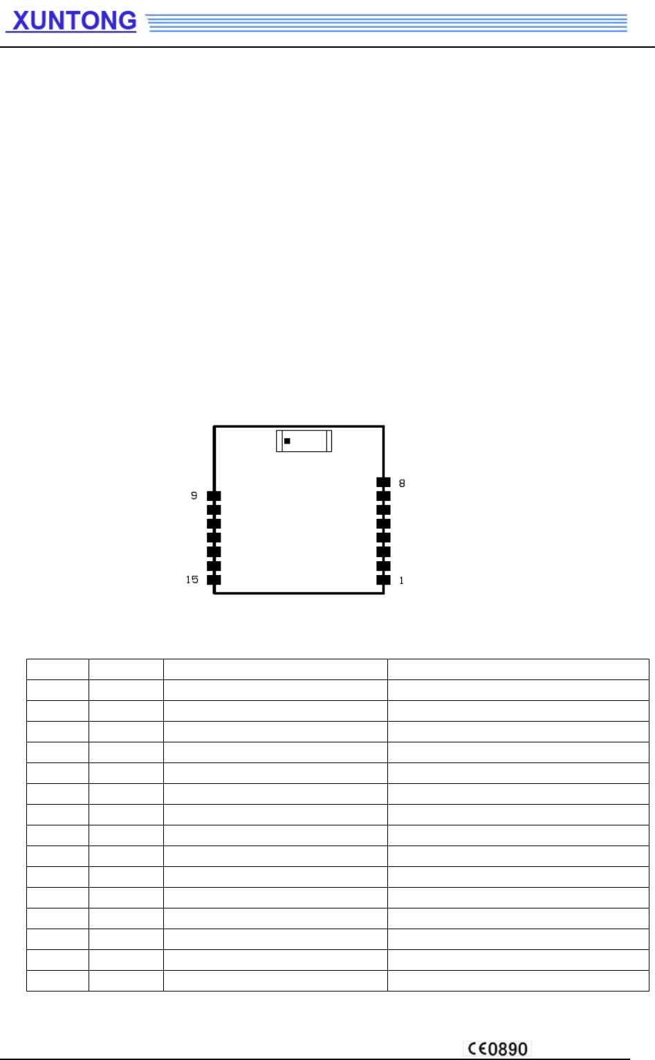
Pin Description of Module(Top View):
Pin No. Name Description Note
1 P0.08 I/O
2 P0.09 I/O
3 P0.12 I/O
4 SWDIO Debug and flash programming I/O
5 SWCLK Debug and flash programming I/O
6 P0.17 I/O
7 P0.18 I/O
8 P0.19 I/O
9 GND Power Ground
10 VDD Power Suply(1.9~3.6V)
11 P0.25 I/O
12 P0.26 I/O ADC IN 0
13 P0.27 I/O ADC IN 1
14 P0.28 I/O
15 P0.29 I/O
COPYRIGHT ©2013 ALL RIGHTS RESERVED LANKE XUNTONG TECHNOLOGY CO.,LTD
TEL: +86 755 26674742 +86 755 26675941 E-mail: nrf@freqchina.com
2
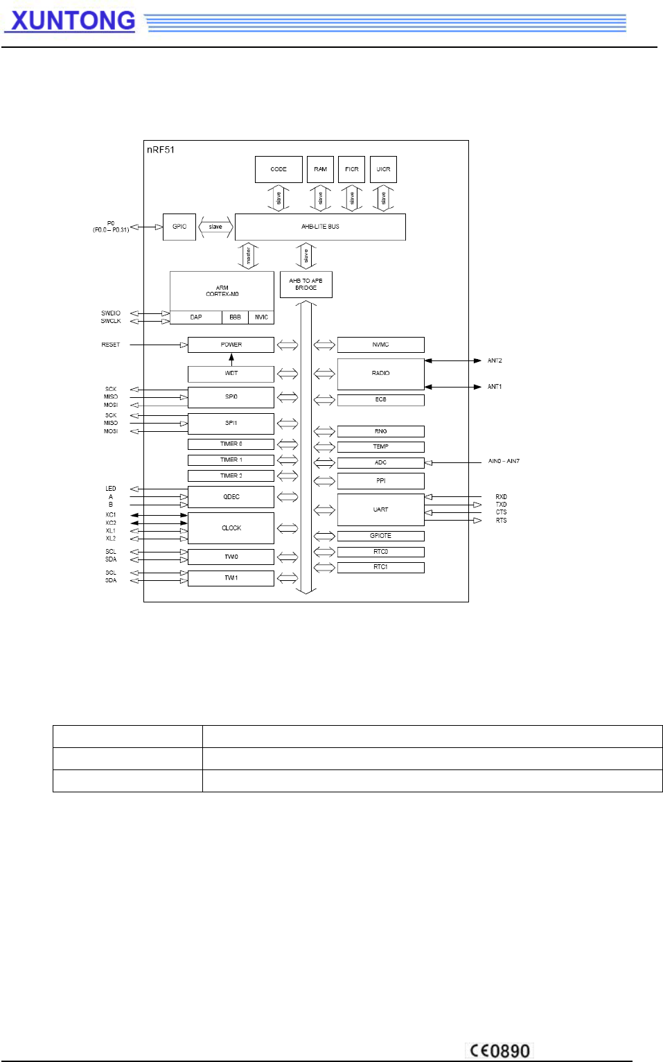
Block diagram:
HW debug and flash programming of Module :
Pin Flash Program interface
SWDIO Debug and flash programming I/O
SWCLK Debug and flash programming I/O
This is the hardware debug and flash programming of module, J-Link Lite support, pleas refer
www.segger.com.
COPYRIGHT ©2013 ALL RIGHTS RESERVED LANKE XUNTONG TECHNOLOGY CO.,LTD
TEL: +86 755 26674742 +86 755 26675941 E-mail: nrf@freqchina.com
3
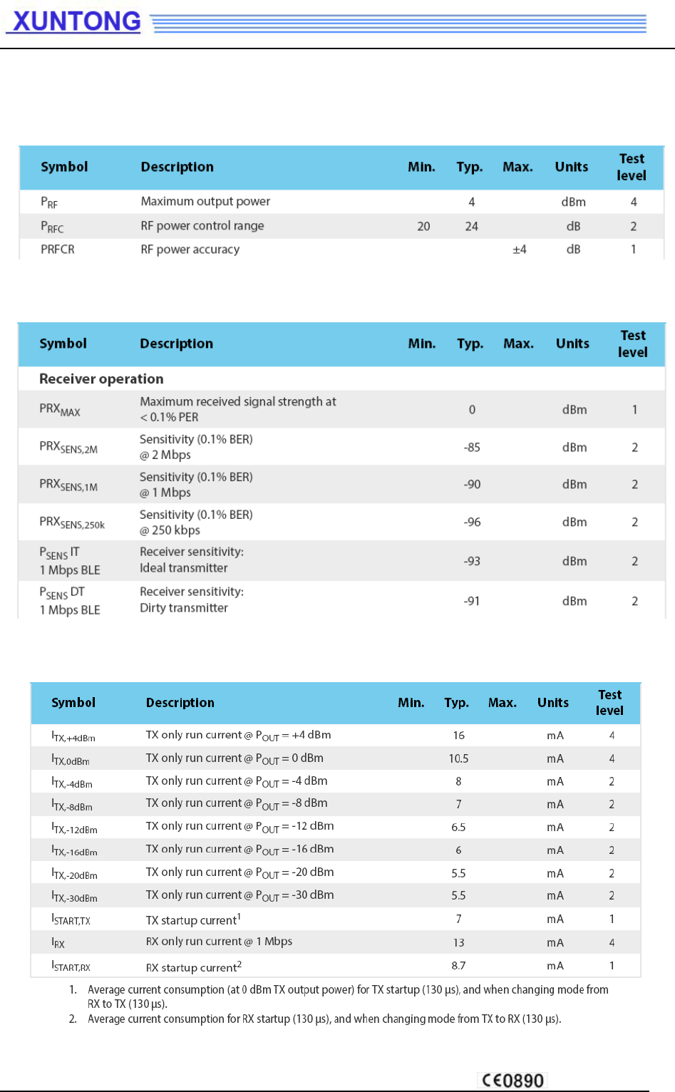
Performance Data:
Transmitter specification:
Receiver specification:
Radio current consumption:
COPYRIGHT ©2013 ALL RIGHTS RESERVED LANKE XUNTONG TECHNOLOGY CO.,LTD
TEL: +86 755 26674742 +86 755 26675941 E-mail: nrf@freqchina.com
4
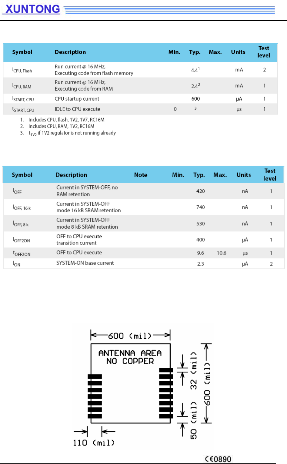
CPU current consumption:
Power management:
For more detail information, please refer nRF51822 datasheet.
PCB Layout(TOP VIEW):
COPYRIGHT ©2013 ALL RIGHTS RESERVED LANKE XUNTONG TECHNOLOGY CO.,LTD
TEL: +86 755 26674742 +86 755 26675941 E-mail: nrf@freqchina.com
5
unit: mil
PIN Description
NO PIN INPUT\
OUTPUT Description
1 EN I
Enabled Pins,External Pull up:
Falling Edge:Module starts Broadcasting, and connect with device
Raising Edge:No matter what status of the module, the module will
enter into deep sleep mode. (420 nA)
2 TX O UART TX
3 RX I UART RX
4 — — Not used
5 — — Not used
6 CTS O
Input signal to wake up MCU (Optional)
0:Means module’s sending data to MCU , Master’s ready to receive
data from Module
1:Means no data sending to MCU, or Module data sending Finished
7 RTS I
Data output request to wake up module
0:Means MCU will send data out, and Module is waiting for the data
from MCU
1:Means no data sending to module, or MCU data sending finished
8 FLOW_CTR O
UART Flow Control:
0:UART can send data to module
1:Module is busy, UART can’t send data to Module
Note:TO Prevent UART data from losing, suggest to check the pin
status before MCU sending data, waiting for a falling edge , then send
data out ( wait for no longer than a broadcasting or an interval ) , see
the Chart 3-1 for reference.
9 GND — Power Ground
COPYRIGHT ©2013 ALL RIGHTS RESERVED LANKE XUNTONG TECHNOLOGY CO.,LTD
TEL: +86 755 26674742 +86 755 26675941 E-mail: nrf@freqchina.com
6

10 VCC — Power Supply’
Positive(3 ~ 3.6V)
11 CFG_MODE I
Select Parameter configuration mode, interval pull up
0:Simple mode:
Input level to set Baud Rate through BAUD_0、BAUD_
Input level to set Connection Interval through CNITV_0、CNITV_1
1:AT command mode:
Sending AT command through UART to set Baud Rate and
Connection Interval 。
12 BAUD_0 I
13 BAUD_1 I
Set Baud Rate(Under Simple Mode),Internal Pull down:
BAUD_0, BAUD_1:
00: 9600
01: 19200
10: 38400
11: 115200
14 CNITV_0 I
15 CNITV_1 I
Set Connection Interval(Under Simple Mode),Internal Pull down:
CNITV_0, CNITV_1:
00: 20ms
01: 100ms
10: 500ms
11: 1000ms
Pls note that ;
1. This User Manual is a guide for OEM /Integrators , is Limited for OEM/Integrator installations
Only.
2. The OEM integrator is responsible for ensuring that the end-user has no manual instruction
to remove or install module
3. Separate approval is required for all other operating configurations, including portable
configurations with respect to Part 2.1093 and different antenna configurations
4. The authorized antennas per Part 15.204 (including antenna specification).
Warning:
This device complies with Part 15 of the FCC Rules. Operation is subject to the following two
conditions: (1) this device may not cause harmful interference, and (2) this device must accept any
interference received, including interference that may cause undesired operation.
changes or modifications not expressly approved by the party responsible for compliance could void
the user’s authority to operate the equipment.
Please notice that if the FCC identification number is not visible when the module is installed inside
another device, then the outside of the device into which the module is installed must also display a
label referring to the enclosed module. This exterior label can use wording such as the following:
“
Contains FCC ID:
2AA72
-
PTR5518
”
7
COPYRIGHT ©2013 ALL RIGHTS RESERVED LANKE XUNTONG TECHNOLOGY CO.,LTD
TEL: +86 755 26674742 +86 755 26675941 E-mail: nrf@freqchina.com

Important Notice:
Reserves the right to make corrections, modifications, and/or improvements to the product and/or
its specifications at any time without notice.
Assumes no liability for the user’s product and/or applications.
Products are not authorized for use in safety-critical applications, including but not limited to
life-support applications.
ATTENTION!
Electrostatic Sensitive Device
Observe Precaution for handling.
8
COPYRIGHT ©2013 ALL RIGHTS RESERVED LANKE XUNTONG TECHNOLOGY CO.,LTD
TEL: +86 755 26674742 +86 755 26675941 E-mail: nrf@freqchina.com