LANKE XUNTONG TECHNOLOGY PTR5518IPX Bluetooth 4.0 module User Manual
LANKE XUNTONG TECHNOLOGY CO.,LTD Bluetooth 4.0 module Users Manual
Contents
- 1. User Manual 1
- 2. User Manual 2
User Manual 1

Coin-size Ultra Low Power Bluetooth 4.0 Low Energy RF Module
Features
Complete Bluetooth 4.0,single mode compliant,Integrated Bluetooth low energy stack/profiles.
2.4 GHz transceiver
•-93 dBm sensitivity in Bluetooth® low energy mode, -96 dBm sensitivity@250kbps,
•13 mA peak RX, 10.5 mA peak TX (0 dBm)
•RSSI (1 dB resolution)
ARM® Cortex™-M0 32 bit processor, 256 kB flash memory, 16 kB RAM.
•275 μA/MHz running from flash memory
•150 μA/MHz running from RAM
•Serial Wire Debug (SWD)
Ultra low current consumption , Flexible Power Management
•Supply voltage range 1.8 V to 3.6 V
•2.5 μs wake-up using 16 MHz RCOSC
•0.4 μA @ 3 V OFF mode
•0.5 μA @ 3 V in OFF mode + 1 region RAM retention
•2.3 μA @ 3 V ON mode, all blocks IDLE
Flexible real-time counter and Two 16 bit and one 24 bit timers with counter mode
AES Coprocessor, Random Number Generator ,Watchdog Timer ,Temperature sensor
Rich set of Peripheral: ADC, SPI, 2-wire , and UART. Programmable Peripheral Interconnect(PPI)
Internal RC Oscillator 32.768 kHz(± 250 ppm).
Configurable I/O mapping (I/O signals can use any pin, Simple layout of external application)
Ultra small size(smaller than CR2032 coin battery), about 15mmx15mmx2.5mm.
PTR5518-IPX
COPYRIGHT ©2017 ALL RIGHTS RESERVED XunTong Technology E-mail: nrf@freqchina.com 1
Typical Applications:
- 2.4 GHz Bluetooth low energy systems
- Sports and leisure equipment
- Mobile phone accessories
- Health Care and Medical
- Consumer Electronics, Game pads
- Human Interface Devices, Remote control
- Building environment control / monitoring
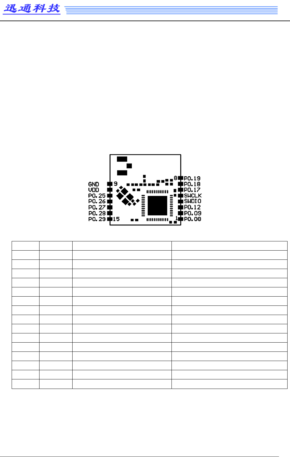
Pin Description of Module
(
Top View
)
:
Pin No.
Name
Description
Note
1
P0.08
I/O
2
P0.09
I/O
3
P0.12
I/O
4
SWDIO
Debug and flash programming I/O
5
SWCLK
Debug and flash programming I/O
6
P0.17
I/O
7
P0.18
I/O
8
P0.19
I/O
9
GND
Power Ground
10
VDD
Power Suply
(
1.9
~
3.6V
)
11
P0.25
I/O
12
P0.26
I/O
ADC IN 0
13
P0.27
I/O
ADC IN 1
14
P0.28
I/O
15
P0.29
I/O
COPYRIGHT ©2017 ALL RIGHTS RESERVED XunTong Technology E-mail: nrf@freqchina.com
2
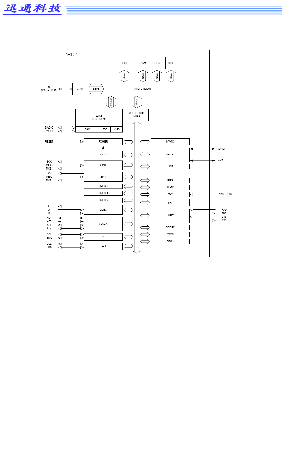
Block diagram:
HW debug and flash programming of Module :
Pin Flash Program interface
SWDIO Debug and flash programming I/O
SWCLK Debug and flash programming I/O
This is the hardware debug and flash programming of module, J-Link Lite support, pleas refer
www.segger.com.
COPYRIGHT ©2017 ALL RIGHTS RESERVED XunTong Technology E-mail: nrf@freqchina.com
3
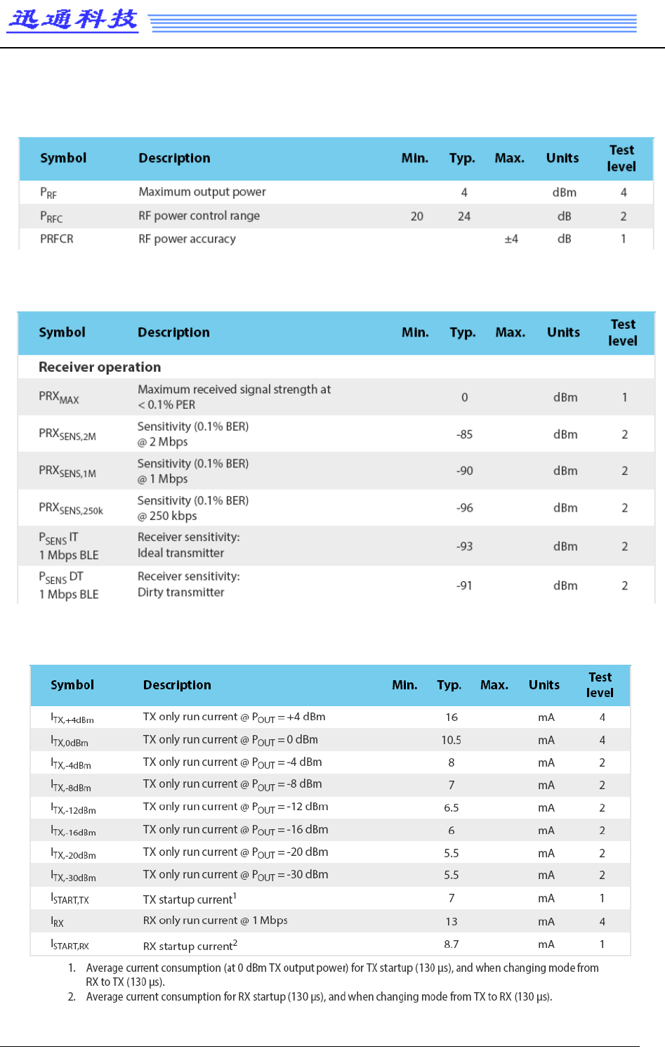
Performance Data:
Transmitter specification:
Receiver specification:
Radio current consumption:
COPYRIGHT ©2017 ALL RIGHTS RESERVED XunTong Technology E-mail: nrf@freqchina.com
4
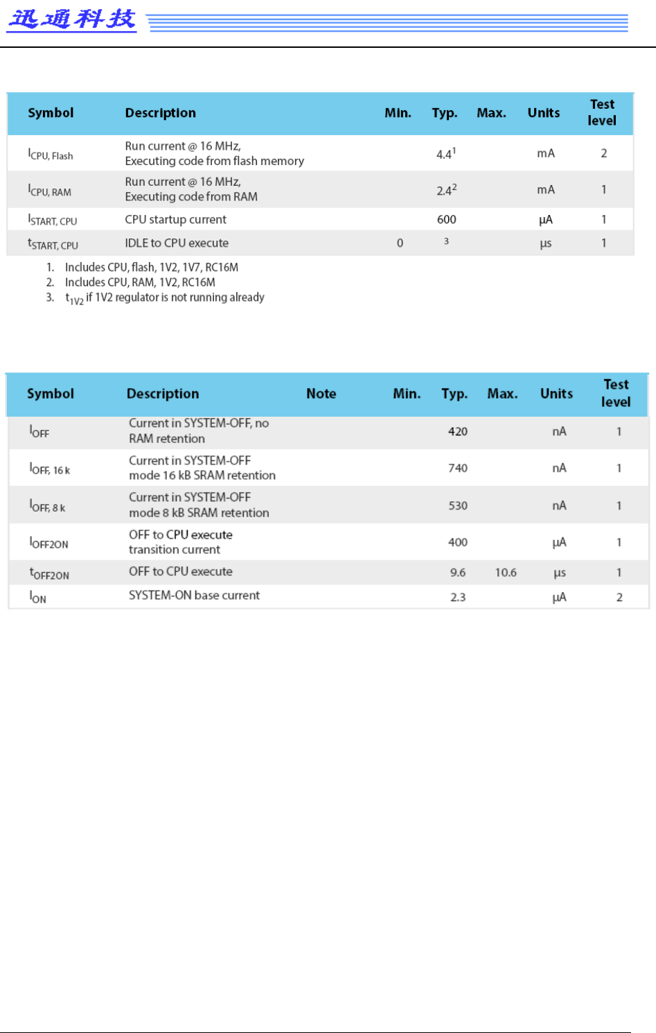
CPU current consumption:
Power management:
For more detail information, please refer nRF51822 datasheet.
COPYRIGHT ©2017 ALL RIGHTS RESERVED XunTong Technology E-mail: nrf@freqchina.com
5
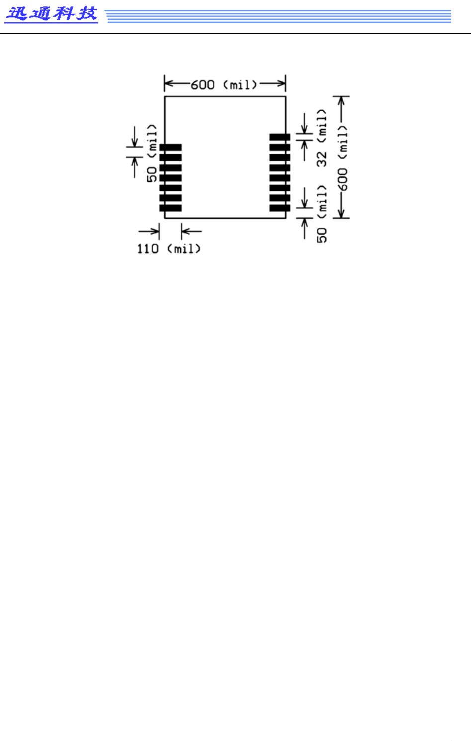
PCB Layout
(
TOP VIEW
)
:
unit: mil
Important Notice:
Reserves the right to make corrections, modifications, and/or improvements to the product and/or
its specifications at any time without notice.
Assumes no liability for the user’s product and/or applications.
Products are not authorized for use in safety-critical applications, including but not limited to
life-support applications.
ATTENTION!
Electrostatic Sensitive Device
Observe Precaution for handling.
COPYRIGHT ©2017 ALL RIGHTS RESERVED XunTong Technology E-mail: nrf@freqchina.com
6