LG Electronics USA 9QK-DMRS3 Wireless Adpter Card User Manual manual
LG Electronics USA Wireless Adpter Card manual
manual

Model Name : RS3_2.4GHz_NAM-SS01 module
Product Description.
The Module is an OEM module (35x35mm) based on the IA3S4. It is a compressed wireless digital
audio transceiver operating in the 2.4GHz bands. The wireless audio link supports 1 stereo audio
stream and comes together with additional features such as: pairing functionality, seamless and bi-
direction transmission of high quality audio, I2S sampling frequency detection, support Sleep mode,
Programmable end-to-end audio latency, Control Channel ability, support no audio detection, Robust
packet error correction.
SYNIC IA3S4 Integrated Wireless Audio Processor
GFSK digital modulation.
Audio format 16bit, 32/44.1/48KHz sampling rate
Digital audio interfaces (I2S and/or S/PDIF)
I2C, SPI control interface
26 pins interface connector (FFC).
Support no audio detection function.
Robust packet error correction.
Low power consumption.
Low audio delay time < 20ms
RF Frequency Bandwidth.
2.4GHz: 2400 – 2485MHz
RF Performance.
For 2.4GHz application (VCC=3.3V, 25°C)
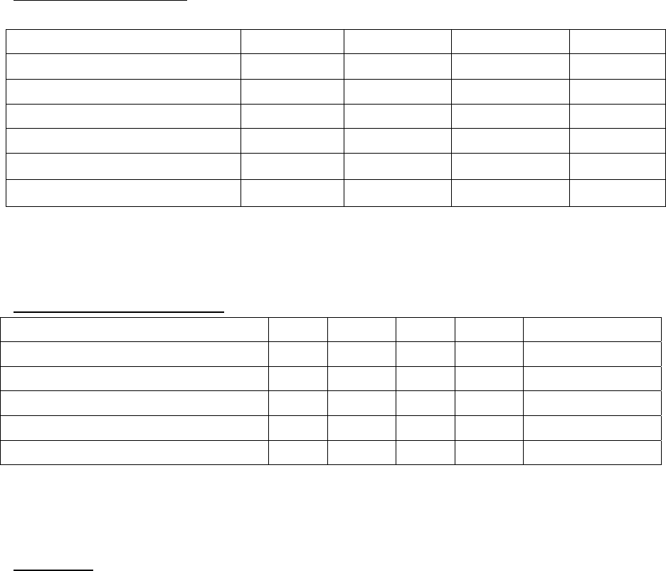
Parameter Min Typ. Max Units
RF Frequency Range 2400 2485 MHz
Available channel 39
Transmission Power 5 7 9 dBm
RF Bandwidth 1 MHz
Rx Sensitivity -80 dBm
Antena Diversity ON
Audio Performance.
Item Min Typ Max Unit Note
SNR @ 1Khz -88 dBr
THD+N @ 1KHz -70 dB
Dynamic Range @ 1KHz -85 dBr
Crosstalk @ 1KHz -100 dB
Frequency Response @ 20Hz to 20KHz -3 0 +3 dB
POWER
- Supply Voltage : 3.1V(Min), 3.3V(Typ), 3.5V(Max)
- Peak to Peak Ripple: 100mV(Max)
- Operating Current: 50mA(Typ)
- Operating Temperature : 0°C (Min) , 25°C (Typ) , 55°C (Max)

26Pin Interface
No. Pin Name I/O Descriptions
1 VCCIO PWR VCC supply
2 GND GND Ground
3 I2S_MCLK I/O System clock pin of I2S signal
4 BLUE_LED I/O GPIO
5 RED_LED I/O GPIO
6 NC I/O Not connected
7 NC I/O Not connected
8 I2S_DATA I/O Data pin of I2S signal
9 NC I/O Not connected
10 I2C_CLK I/O Clock pin of I2C control signal
11 I2C_DATA I/O Data pin of I2C control signal
12 SPI_DI I/O Data input pin of SPI interface
13 SPI_DO I/O Data out pin of SPI interface
14 SPI_CLK I/O Clock pin of SPI interface
15 SPI_CS I/O Chip select pin of SPI interface
16 SPI_WP I/O Write protect pin of SPI interface, low active
17 RESET I Reset pin of IA3, low active
18 P_SENSE I/O GPIO
19 P_CTL I/O GPIO
20 PWM_RST I/O GPIO
21 AMP_PDN I/O GPIO
22 AMP_SD I/O GPIO
23 Wireless_Ready I/O GPIO
24 I2S_BCK I/O BCK pin of I2S signal
25 GND GND Ground
26 I2S_LRCK I/O LRCK pin of I2S

FCC Information
This device complies with part 15 of the FCC Results. Operation is subject to the
following two conditions :
(1) This Device may not cause harmful interface, and
(2) This device must accept any interference received, including interference that
may cause undesired operation.
Note: This equipment has been tested and found to comply with the limits for CLASS B digital
device, pursuant to Part 15 of FCC Rules. These limits are designed to provide reasonable
protection against harmful interference when the equipment is operated in a commercial
environment This equipment generates, uses and can radiate radio frequency energy and, if not
installed and used in accordance with the instructions, may cause harmful interference to radio
communications. However, there is no guarantee that interference will not occur in a particular
installation. If this equipment does cause harmful interference to radio or television reception,
which can be determined by turning the equipment off and on, the user is encouraged to try
correct the interference by one or more of the following measures:
1.1. Reorient or relocate the receiving antenna.
1.2. Increase the separation between the equipment and receiver.
1.3. Connect the equipment into an outlet on a circuit different from that to which receiver is
connected.
1.4. Consult the dealer or experienced radio/TV technician for help.
WARNING
Changes or modifications not expressly approved by the manufacturer could void the
user’s authority to operate the equipment.
“CAUTION : Exposure to Radio Frequency Radiation.
Antenna shall be mounted in such a manner to minimize the potential for human
contact during normal operation. The antenna should not be contacted during operation
to avoid the possibility of exceeding the FCC radio frequency exposure limit.