LG Electronics USA EBR64966501 Remote Control Module User Manual Manual
LG Electronics USA Remote Control Module Manual
Manual
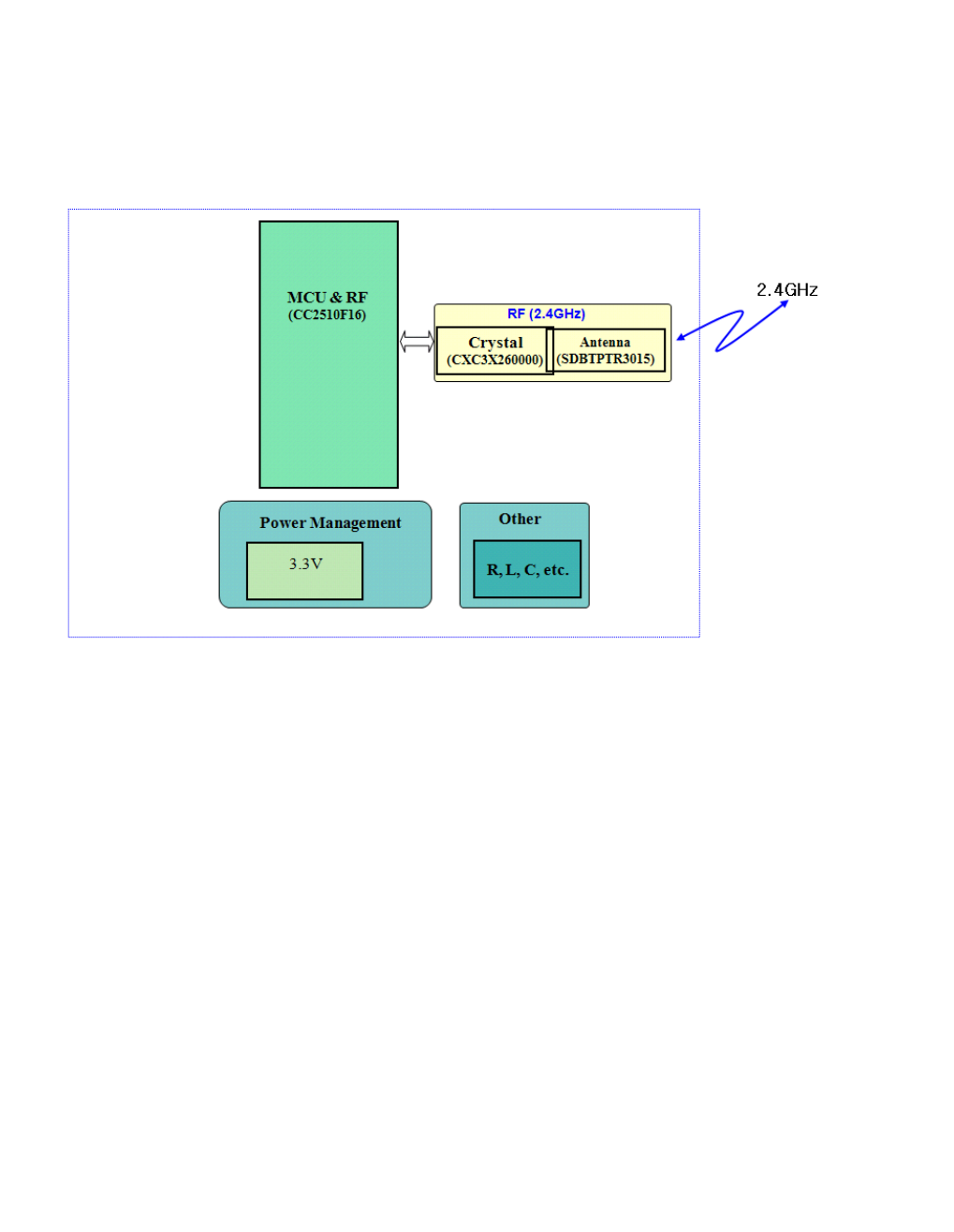
Description of Functional Blocks
EBR64966501
Rev A, Jan 2010
< EBR64966501 >
LG Electronics
Hanyang Univ. 1271, Sa-dong, Sangrok-gu ,
Ansan-si, Gyeonggi-do 426-791, Korea
Tel:82-31-436-7653
Fax:82-31-436-7991
www.lge.com
Copyright ⓒ 2010, LG Electronics Co., Ltd. http:\\www.lge.com All
specification are preliminary and LG Innotek reserves the right to change these without notice.

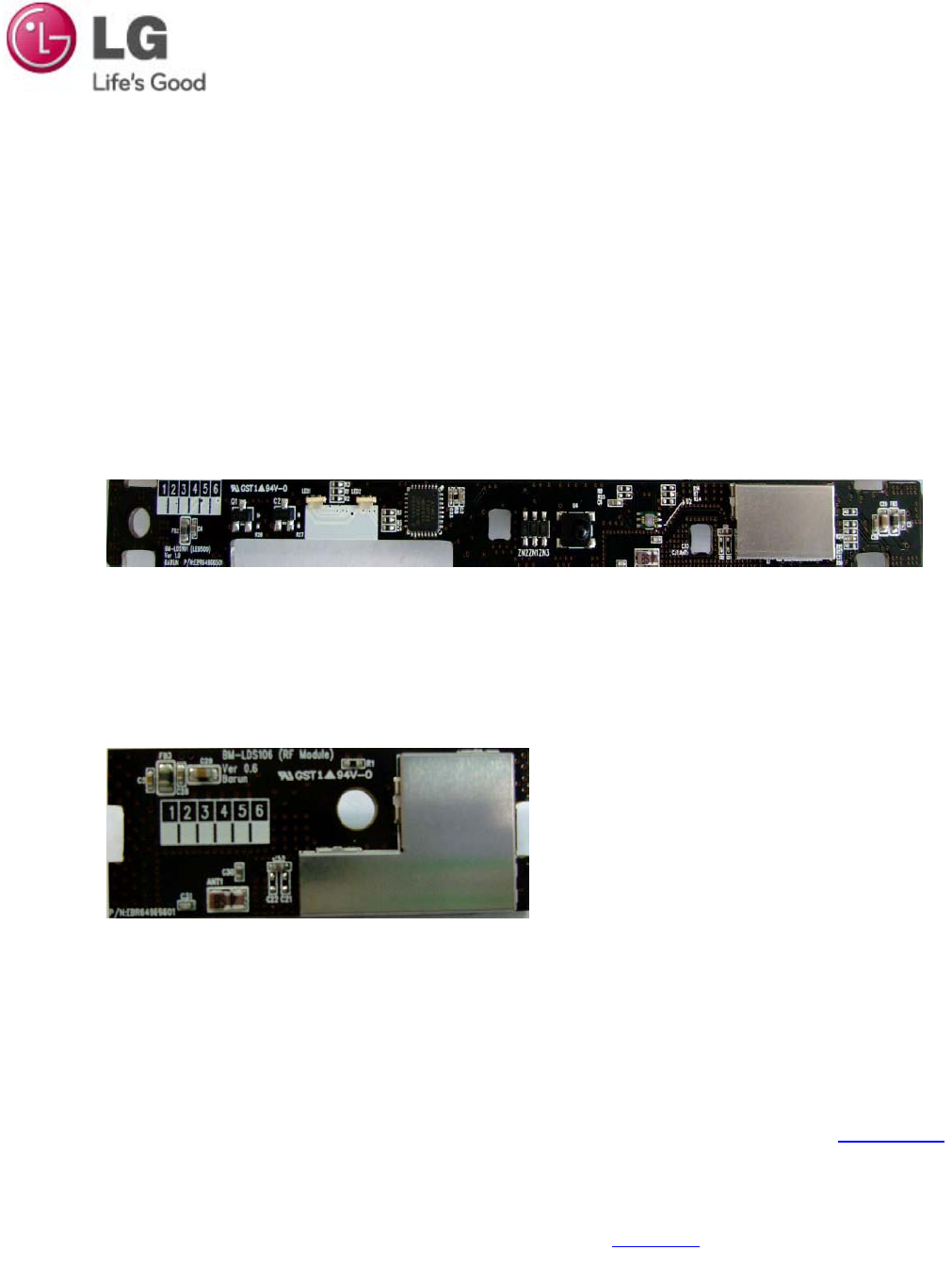
■ EBR64966501
1. RF Transmitter Block
1.1 Transmitter Feature
The transmitter part of RF-Receiver is internally based on direct synthesis of the RF
frequency. The frequency synthesizer includes a completely on-chip LC VCO and a 90
degrees phase shifter for generating the I / Q LO signals to the down-conversion mixers in
receive mode. The baseband transmit data is digitally 2-FSK/GFSK/MSK modulated in the
modem block and up-converted to the 2.4 GHz ISM band in the transmitter path. The
transmitter path consists of Modulator, I/Q up-conversion through frequency synthesizer,
high-output power amplifier (PA). RF-Receiver also uses MSK modulation schemes for
250kbps.
1.1.1 Digital Modulator
RF-Receiver supports frequency and phase shift modulation formats (2-FSK/GFSK/MSK).
It is suited for systems targeting compliance with digital modulation systems as defined by
FCC part 15.247. Also, the sync word is a 16 bit configurable field (can be repeated to get a 32
bit) that is automatically inserted at the start of the packet by the modulator in transmit mode.
1.1.2 Digital Demodulator and Symbol Synchronizer and Data Decision
The RF-Receiver contains an advanced and highly configurable demodulator. Channel
filtering and frequency offset compensation is performed digitally. When using MSK
modulation, the demodulator will compensate for the offset between the transmitter and
receiver frequency, within certain limits, by estimating the centre of the received data. The
bit synchronization algorithm extracts the clock from the incoming symbols. Byte
synchronization is achieved by a continuous sync word search. The demodulator uses this
field to find the byte boundaries in the stream of bits.
1.1.3 Power Amplifier
The integrated PA for the RF-Receiver can transmit at a maximum power of +1dBm. In
some applications it may be necessary to extend the link range. Adding an external power
amplifier is the most effective way of doing this.The power amplifier should be inserted
between the antenna and the balun, and two. T/R switches are needed to disconnect the
PA in RX mode.
■ EBR64966501
2. RF Receiver Block
2.1 Receiver Feature
The RF-Receiver features a low-IF receiver. The received RF signal is amplified by
the low noise amplifier (LNA) and down-converted in quadrature (I and Q) to the
intermediate frequency (IF). At IF, the I/Q signals are digitized by the ADCs.
Automatic gain control (AGC), fine channel filtering, demodulation bit/packet
synchronization are performed digitally.
2.1.1 Digital Demodulator and Symbol synchronizer
The digital demodulator and bit synchronizer takes the low IF received signal and
performs an optimal frequency tracking and bit/byte symbol synchronization
algorithm as like a transmit part. If the sync word detection in RX is enabled, the
sync word will also function as a system identifier since only packets with the
correct predefined sync word symbol will be received.
2.1.2 Received Signal Qualifiers and Link Quality Information
The RF-Receiver has several qualifiers that can be used to increase the likelihood
that a valid sync word is detected. Preamble Quality Indicator for detecting preambles
and improved protection against sync word detection in random noise. To generate
the RSSI level, the signal level in the channel is estimated. Data filtering is also
included for enhanced performance

■ EBR64966501
3. Baseband Core
The RF-Receiver is based on the industry leading CC2500 radio core. It has few external
components (On-chip frequency synthesizer, no external filters or RF switch needed). It also flexibly
manage for packet oriented systems (On-chip support for sync word detection, address check,
flexible packet length, and automatic CRC handling). With Supports use of DMA for both RX and TX
it results in minimal CPU intervention even on high data rates. In addition to It is programmable for
channel filter bandwidth
4. Microprocessor Unit
The RF-Receiver includes an 8-bit CPU core which is an enhanced version of the industry
standard 8051 core. It has 16kB in-system programmable flash, and 2 kB RAM. Also it supports
various and useful peripheral components (I2S interface, 7 - 12 bit ADC with up to eight inputs,
128-bit AES security coprocessor, Powerful DMA functionality, Two USARTs, 16-bit timer with
DSM mode, Three 8-bit timers, Hardware debug support)
5. Crystal Interface and Clock Generation
The RF-Receiver uses a fractional-N synthesizer to generate the radio frequencies,
clock, and data packet timing. This enables it to operate from any of a multitude of
frequency sources. System clock source is either a high speed crystal oscillator (24 -
27 MHz) or a high speed RC oscillator (12 - 13.5 MHz). The high speed crystal
oscillator must be used when the radio is active. To reduce system power
consumption, clock source for ultra-low power operation can be either a low-power RC
oscillator or external 32.768KHz crystal. The RF-Receiver’s reference frequency
reference setting is a 26-MHz crystal in active mode and internal low RC oscillator in
low power mode.
This device complies with part 15 of FCC Rules. Operation is subject to the following two conditions:
1. This device may not cause harmful interference received.
2. This device must accept any interference received. Including interference that may cause undesired operation.
FCC WARNING
This equipment may generate or use radio frequency energy.
Changes or modifications to this equipment may cause harmful interference unless the modifications are expressly
approved in the instruction manual. The user could lose the authority to operate this equipment if an unauthorized
change or modification is made.
To satisfy FCC exterior labeling requirements, the following text must be placed on the exterior Of the end product.
Contains Transmitter Module FCC ID: BEJEBR64966501
CAUTION: This device and it’s antenna(s) must not be co-located or operated in conjunction with any other antenna
or transmitter. End users cannot modify this transmitter device. Any Unauthorized modification could void the user’s
authority to operate this device.