LG Electronics USA GEN21NA AVN Modem Module User Manual
LG Electronics USA AVN Modem Module Users Manual
Users Manual

1/11
Technical Specification
(TM03LNNAHK0)
2/11
History
Ver.
Date
Contents
Written
by
Checked
by
Approved
by
Note
1.0
2016.12.16

3/11
Contents
1. Product Introduction..................................................................................................... 4
1.1 Block Diagram .................................................................................................... 5
1.2 Environmental Specifications .............................................................................. 5
1.3 Electrical Specifications ...................................................................................... 5
1.3.1 Absolute Maximum and ESD Ratings ........................................................... 5
1.3.2 Current Consumption ................................................................................... 6
1.4 Mechanical Specifications ................................................................................. 6
1.4.1 Physical Dimensions and Connection Interface ........................................... 6
1.4.2 Mechanical Drawing ..................................................................................... 7
2. Pin Definitions.............................................................................................................. 8
3 RF Specification ........................................................................................................... 9
3.1. LTE B4, B13 Specification ................................................................................. 9
3.2. CDMA BC0, BC1 Specification..…………………………………………………… 10
4/11
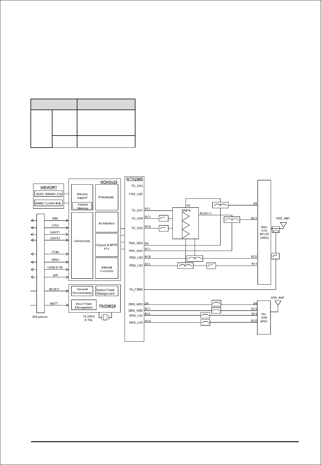
1. Product Introuction
The TM03LNNAHK0 are designed for the automotive industry. They support LTE and CDMA
air Interface standards. The TM03LNNAHK0 are based on the Qualcomm MDM9628 wireless
chipsets and support the following bands.
Table 1. Supported Band
Region
US
Band
LTE
B4/B13
CDMA
BC0/BC1
1.1 Block Diagram
Figure 1.1. TM03LNNAHK0 Block diagram
5/11
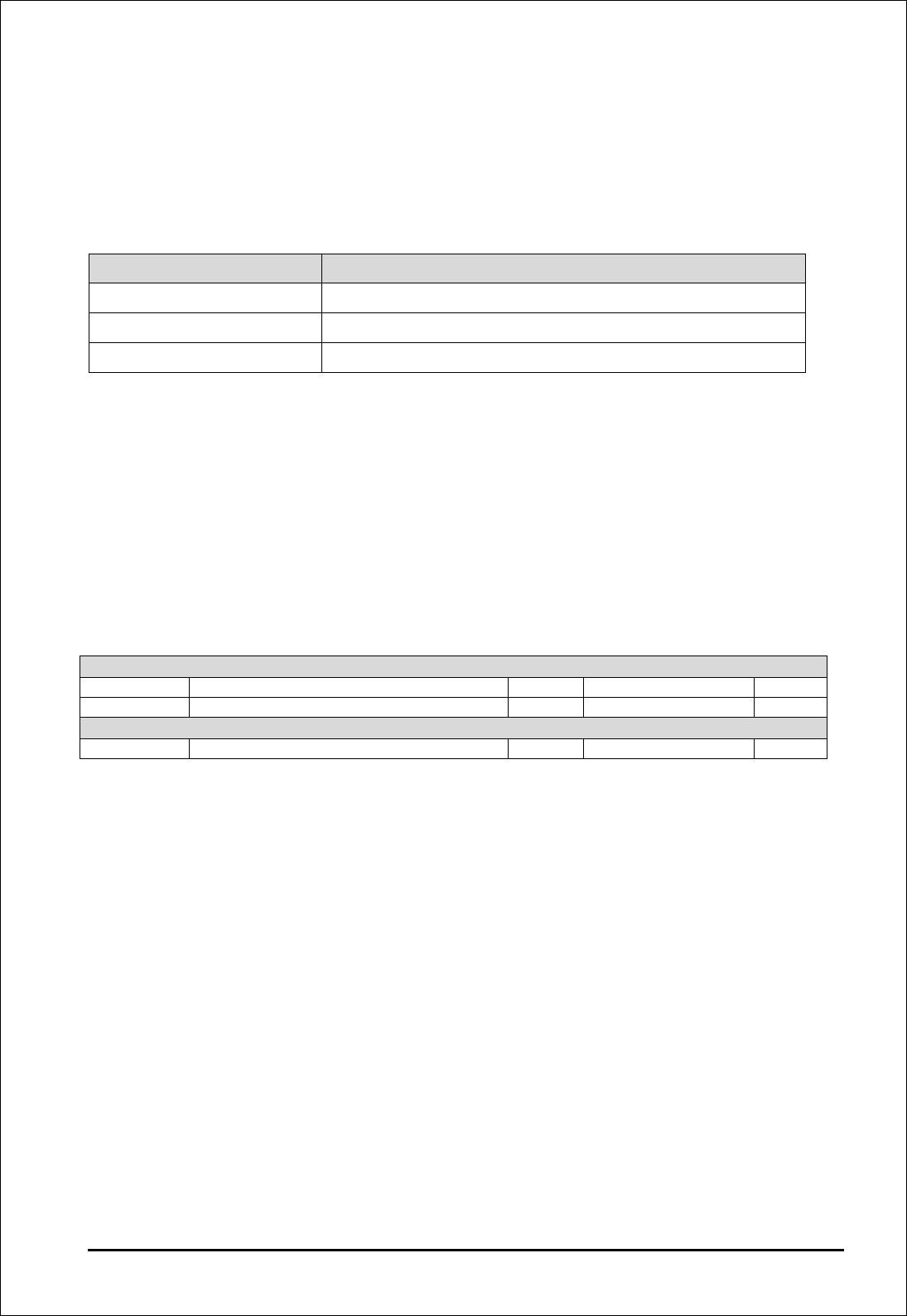
1.2 Environmental Specifications
The environmental specification for operating and storage of the TM03LNNAHK0 are defined
in the the table below.
Table 2. Environmental Specifications
Parameter
Temperature Range
Operating Temperature
-40℃ to 85℃
Storage Temperature
-40℃ to +90℃
Humidity
95% or less
1.3 Electrical Specifications
This section provides details for some of the key electrical specifications of the
TM03LNNAHK0 embedded modules.
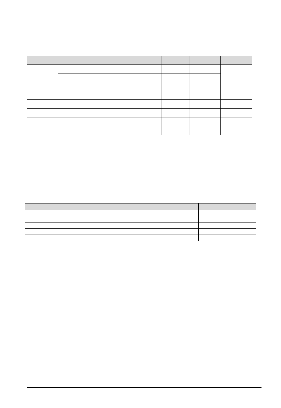
1.3.1 Absolute Maximum Rating and ESD Ratings
This section defines the Absolute Maximum and Electrostatic Discharge (ESD) Ratings of the
TM03LNNAHK0 embedded modules.
Warning: If these parameters are exceeded, even momentarily, damage may occur to the
device.
Table 3. Absolute Maximum Ratings
Parameter
Min
Max
Units
+4.0_VPWR
Power Supply Input
-
4.4V
V
VIN
Voltage on any digital input or output pin
-
VREG_MDME+0.5
V
ESD Ratings
ESD1)
Primary, Diversity antenna pads - Contact
10
kV
1) The ESD Simulator configured with 330pF, 2000Ω.
Caution: The TM03LNNAHK0 embedded modules are sensitive to Electrostatic Discharge.
ESD countermeasures and handling methods must be used when handling the
TM03LNNAHK0 devices.
6/11
1.3.2 Current Consumption
Table 4. TM03LNNAHK0 Current Consumption (TBD)
Mode
Parameter
Typical
Max
Units
LTE
Band4, Max TX Output /Full RB
600
650
mA
Band13, Max TX Output /Full RB
550
600
CDMA
800MHz
550
600
mA
1900MHz
600
650
LTE
Idle, Registered
1.8
2.2
mA
CDMA
Idle, Registered
1.8
2.2
mA
LTE
Sleep Mode, Average Current
1.8
2.2
mA
CDMA
Sleep Mode, Average Current
1.8
2.2
mA
1.4 Mechanical Specifications
1.4.1 Physical Dimensions and Connection Interface
The TM03LNNAHK0 embedded modules are a Land Grid Array (LGA) form factor device. The
device does not have a System or RF connectors. All electrical and mechanical connections
are made via the 323 pad TM03LNNAHK0 on the underside of the PCB.
Table5. TM03LNNAHK0 Embedded Module Dimensions
Parameter
Nominal
Max
Units
Overall Dimension
34 x 40
34.35 x 40.35
mm
Overall Module Height
3.5
3.85
mm
PCB Thickness
1.0
1.1
mm
Flatness Specification
0.1
mm
Weight
TBD
g
7/11
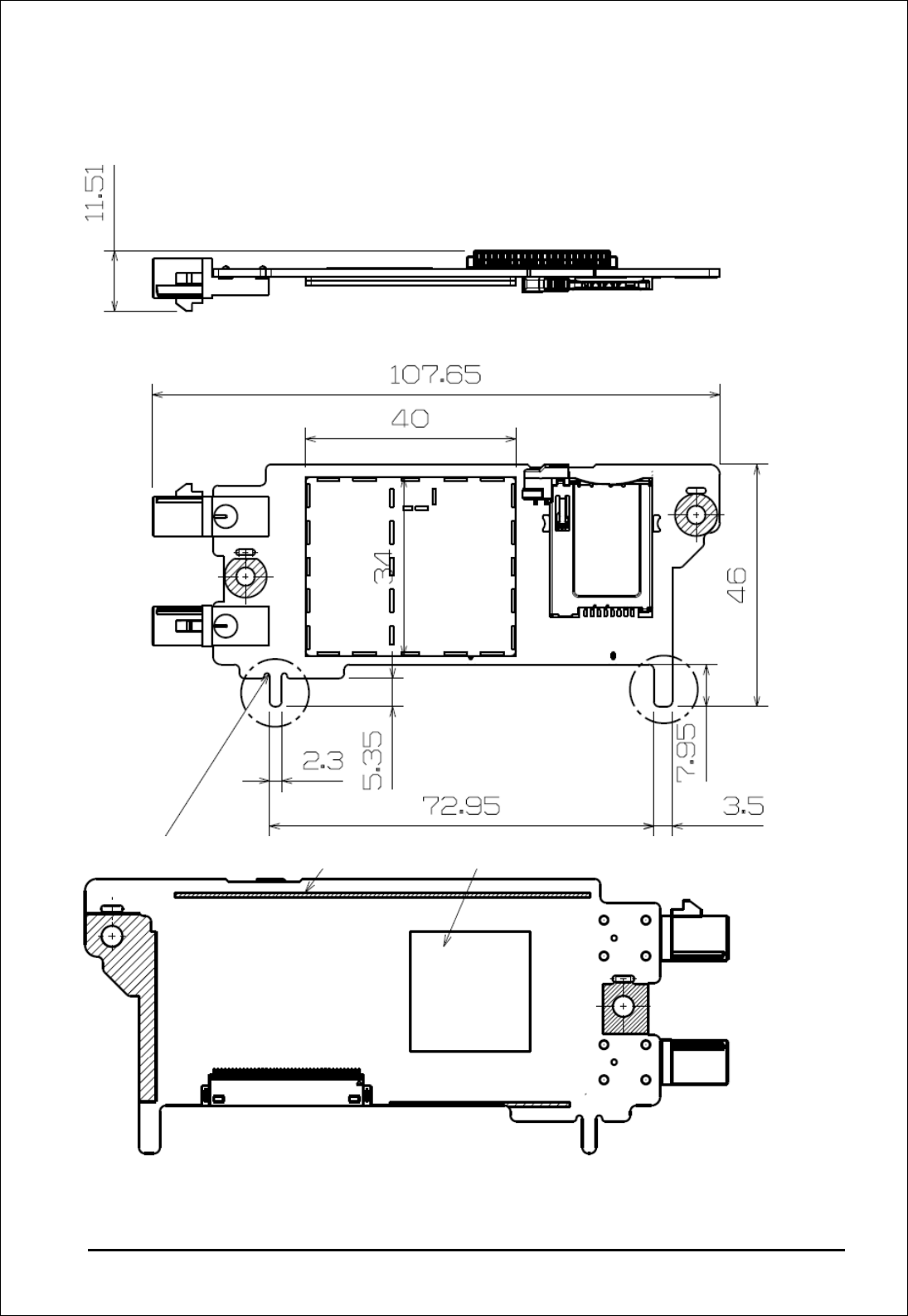
1.4.2 Mechanical Drawing
1.4.2.1 Carrier PCB
[TOP View]
[Bottom View]
8/11
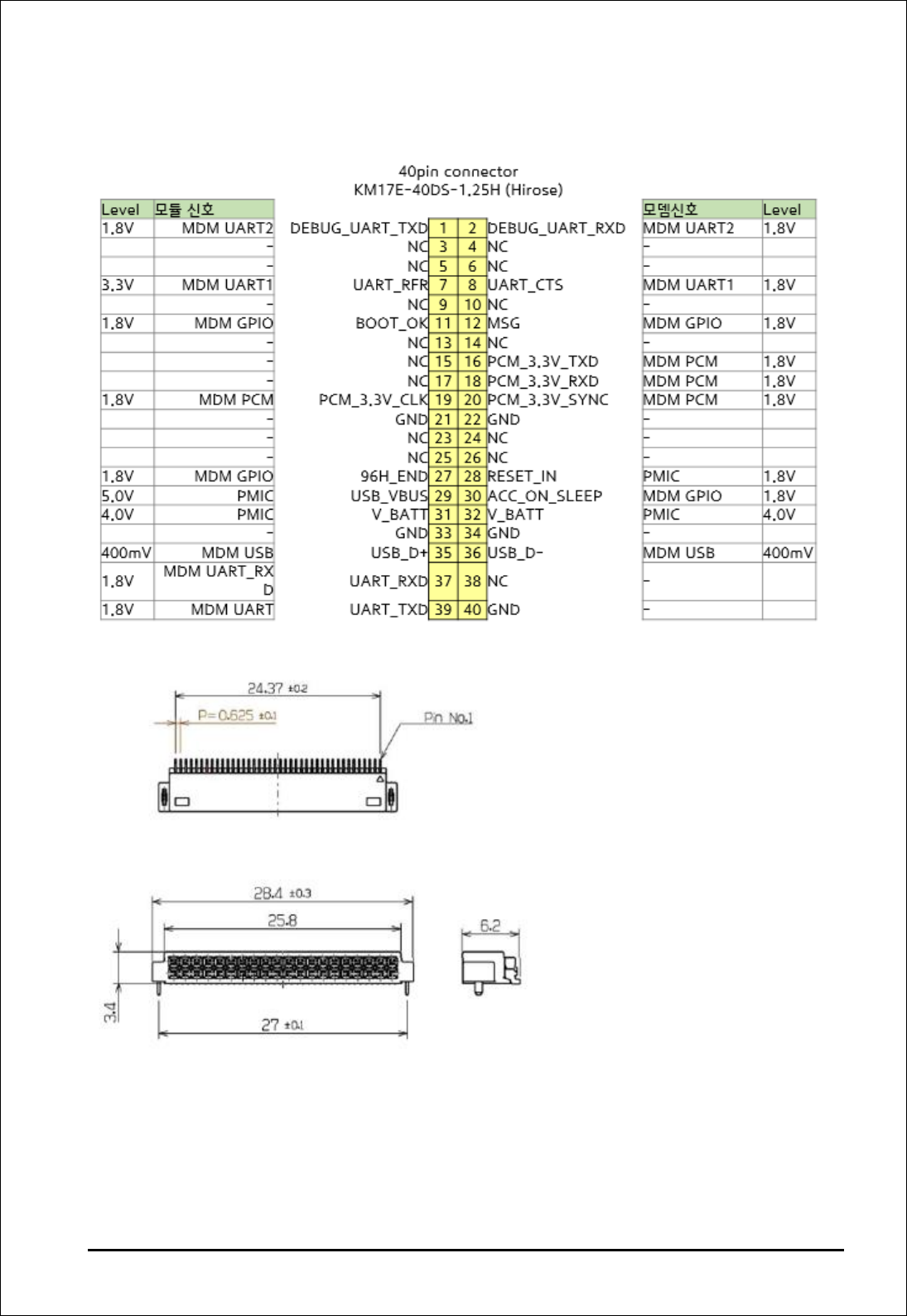
2. Pin Definitions
Table6. PIN Definitions
9/11
3. RF Specification
The specifications for the LTE and CDMA interfaces are defined.
TM03LNNAHK0 is designed to be compliant with the standard shown in the table below.
Table20. Standards Compliance
Technology
Standards
LTE
• 3GPP Release 8
CDMA
• 3GPP2 Release IxEVDO, REV.H
3.1 LTE B4, B13 Specification
3.1.1 LTE TX Output Power
The Maximum / Minimum Transmitter Output Power of the TM03LNNAHK0 are specified in
the following table.
Table21. Conducted TX (Transmit) Max output Power Tolerances – LTE Bands
BAND
Method (UL CH)
Specification
BAND4
UE Maximum
Output Power
Measure Max and Min and Min Transmit Power of
Low Channel (20000)
Max Power : 20.3~25.7dBm
Min Power : ≤ -39dBm
Measure Max and Min Transmit Power of Mid
Channel (20175)
Max Power : 20.3~25.7dBm
Min Power : ≤ -39dBm
Measure Max and Min Transmit Power of High
Channel (20350)
Max Power : 20.3~25.7dBm
Min Power : ≤ -39dBm
BAND13
UE Maximum
Output Power
Measure Max and Min and Min Transmit Power of
Low Channel (23230)
Max Power : 20.3~25.7dBm
Min Power : ≤ -39dBm
3.1.2 LTE RX Sensitivity
The Receiver Sensitivity of the TM03LNNAHK0 are specified in the following table.
Table22. Conducted RX (Receive) Sensitivity – LTE Bands
BAND
Method (DL CH)
Specification
BAND 4
Reference
sensitivity
level(DUAL)
Measure BLER of Low Channel (2000) in Band4
sensitivity : ≤-97
BLER : ≤ 5%
Measure BLER of Mid Channel (2175) in Band4
sensitivity : ≤-97
BLER : ≤ 5%
Measure BLER of High Channel (2350) in Band4
sensitivity : ≤-97
BLER : ≤ 5%
BAND 13
Reference
Measure BLER of Low Channel (23230) in Band13
sensitivity : ≤-94
BLER : ≤ 5%
10/11
sensitivity
level(DUAL)
3.2 CDMA 800/1900 Specification
3.2.1 CDMA TX Output Power
The Maximum Transmitter Output Power of the TM03LNNAHK0 are specified in the
following table.
Table23. Conducted TX (Transmit) Max output Power Tolerances – CDMA Bands
Item
Method (DL CH)
Specification
CDMA800
Power Level
Measure Max Transmit Power of Low Channel
(CH=384) in CDMA Mode
Max Power : 23~30dBm
Measure Max Transmit Power of Middle Channel
(CH=779) in CDMA Mode
Max Power : 23~30dBm
Measure Max Transmit Power of High Channel
(CH=1013) in CDMA Mode
Max Power : 23~30dBm
PCS1900
Power Level
Measure Max Transmit Power of Low Channel
(CH=25) in DCS1900 Mode
Max Power : 23~30dBm
Measure Max Transmit Power of Middle Channel
(CH=600) in DCS1900 Mode
Max Power : 23~30dBm
Measure Max Transmit Power of High Channel
(CH=1175) in DCS1900 Mode
Max Power : 23~30dBm
3.2.2 CDMA RX Sensitivity
The Receiver Sensitivity of the TM03LNNAHK0 are specified in the following table.
Table24. Conducted RX (Receive) Sensitivity – CDMA Bands
Item
Method (DL CH)
Specification
CDMA800
BER(Bit Error
Rate)
Measure BER of Low Channel (CH=384)
in EGSM Mode
0.5% @≤-104dBm
Measure BER of Middle Channel (CH=779)
in EGSM Mode
0.5% @≤-104dBm
Measure BER of High Channel (CH=1013)
in EGSM Mode
0.5% @≤-104dBm
PCS1900
BER(Bit Error
Rate)
Measure BER of Low Channel (CH=25)
in PCS1900 Mode
0.5% @≤-104dBm
Measure BER of Middle Channel (CH=600)
in PCS1900 Mode
0.5% @≤-104dBm
Measure BER of High Channel (CH=1175)
in PCS1900 Mode
0.5% @≤-104dBm

11/11
<Warning Statements>
Any changes or modifications not expressly approved by the party responsible for
compliance could void the user's authority to operate this equipment.
RF Exposure Statement
The antenna(s) must be installed such that a minimum separation distance of at least 20 cm
is maintained between the radiator (antenna) and all persons at all times. This device must
not be co-located or operating in conjunction with any other antenna or transmitter.
The highest permitted antenna gains including cable loss for use with this device are: CDMA
800 : 0.89 dBi, CDMA1900 : 3.20 dBi, LTE Band 4: 2.41 dBi, LTE Band 13: 0.42 dBi.
End Product Labeling
The module is labeled with its own FCC ID. If the FCC ID is not visible when the module is
installed inside another device, then the outside of the device into which the module is
installed must also display a label referring to the enclosed module. In that case, the final
end product must be labeled in a visible area with the following:
“Contains FCC ID: BEJGEN21NA
OEM Responsibilities to comply with FCC Regulations
The module has been certified for integration into products only by OEM integrators under
the following condition:
- The antenna(s) must be installed such that a minimum separation distance of at least 20
cm is maintained between the radiator (antenna) and all persons at all times.
- The transmitter module must not be co-located or operating in conjunction with any other
antenna or transmitter except in accordance with FCC multi-transmitter product procedures.
As long as the two condition above is met, further transmitter testing will not be required.
However, the OEM integrator is still responsible for testing their end-product for any
additional compliance requirements required with this module installed (for example, digital
device emissions, PC peripheral requirements, etc.).
IMPORTANT NOTE: In the event that these conditions can ’ t be met (for certain
configurations or co-location with another transmitter), then the FCC authorization is no
longer considered valid and the FCC ID can’t be used on the final product. In these
circumstances, the OEM integrator will be responsible for re-evaluating the end product
(including the transmitter) and obtaining a separate FCC authorization.
Manual Information To the End User
The OEM integrator has to be aware not to provide information to the end user regarding
how to install or remove this RF module or change RF related parameters in the user
manual of the end product.