LG Electronics USA LEO2-B LTE User Equipment User Manual LEO2 Platform Hardware Manual
LG Electronics USA LTE User Equipment LEO2 Platform Hardware Manual
Users Manual
Updated
2008-09-08
File
LEO2 Platform Hardware Manual
Rev.
V1.0
Title
LEO2-B Platform Hardware Manual
Type
Manual
LGE Proprietary i MCTR Lab.
ABSTRACT 1
This document is hardware manual for LEO2-B Platform board. Contents of this document are 2
descriptions of each blocks and usage directions. It is recommended to peruse this manual before 3
operating LEO2-B Platform 4
5
6
HISTORY 7
Rev
Status
Date Author Contents
8
KEY WORDS 9
10
11
©Copyright, 2008 By LG Electronics Inc. All rights reserved.
No part of this document may be reproduced in any way, or by any means, without
the express written permission of LG Electronics Inc.
Mobile Communication Technology Research Lab.
533 Hogye-dong, Dongan-gu, Anyang-shi,
Kyongki-do, KOREA

Updated
2008-09-08
File
LEO2 Platform Hardware Manual
Rev.
V1.0
LGE Proprietary ii MCTR Lab.
1
2
3
4
5
6
7
8
9
10
11
12
13
14
15
16
17
18
19
20
21
22
23
24
25
26
27
28
29
30
31
32
33
34
35
36
37
38
39
40
41
42
43
44
[Notice] 45
1. The product described in this manual may be modified without prior notice for reliability, 46
functionality or design improvement. 47
2. Information contained in this manual is correct and reliable, but LG shall not be held 48
responsible for damage due to the use of information, product or circuit or infringement of 49
property rights or other rights. 50
3. This manual does not grant users the property rights and other rights of the third party or 51
LG Electronics Inc. 52
4. No part of this manual may be transcribed or duplicated without the written permission of 53
LG Electronics Inc. 54
5. The appearance of the product shown in this manual may slightly differ from that of the 55
actual product. 56

Updated
2008-09-08
File
LEO2 Platform Hardware Manual
Rev.
V1.0
LGE Proprietary iii MCTR Lab.
CONTENTS 1
1. Introduction............................................................................................................................... 1 2
1.1 Scope ..................................................................................................................................... 1 3
1.2 Terminology............................................................................................................................ 1 4
1.3 Trademark List........................................................................................................................ 1 5
1.4 Special Mark........................................................................................................................... 1 6
2. Features and top level diagram ................................................................................................. 2 7
2.1 Features ................................................................................................................................. 2 8
2.2 Photograph of the LEO2-B platform board............................................................................... 2 9
2.3 Top level block diagram .......................................................................................................... 3 10
2.4 Placement map....................................................................................................................... 3 11
3. Block description....................................................................................................................... 4 12
3.1 FPGA subsystem .................................................................................................................... 4 13
3.2 ARM subsystem...................................................................................................................... 4 14
3.3 Debugger Interface ................................................................................................................. 5 15
3.4 RF Interface............................................................................................................................ 6 16
3.5 Reference Clock ..................................................................................................................... 7 17
3.6 Reset ...................................................................................................................................... 8 18
3.7 Application interface................................................................................................................ 8 19
3.8 Power Supplies....................................................................................................................... 9 20
4. DIP switch, LED and logic probing connector ............................................................................ 9 21
4.1 ARM Processor debugging configuration switch setting........................................................... 9 22
4.2 General purpose LED indication........................................................................................... 10 23
4.3 Logic probing connector....................................................................................................... 11 24
5. Description of Smart antenna and beam forming modes if applicable ..................................... 12 25
6. Reference ............................................................................................................................ 123 26
27
Updated
2008-09-08
File
LEO2 Platform Hardware Manual
Rev.
V1.0
LGE Proprietary iv MCTR Lab.
1
FIGURES 2
Figure 1. Photograph of LEO2-B platform........................................................................................ 2 3
Figure 2. Top level block diagram .................................................................................................... 3 4
Figure 3. Placement map of LEO2-B ............................................................................................. 3 5
Figure 4. ARM processor Block ..................................................................................................... 4 6
Figure 5. RF interface on LEO2-B platform board ............................................................................ 6 7
Figure 6. Block diagram of RF daughter board................................................................................. 6 8
Figure 7. Block diagram of clock distribution .................................................................................... 7 9
Figure 8. Block diagram of platform board reset scheme.................................................................. 8 10
Figure 9. Block diagram of application interface............................................................................... 8 11
Figure 10. Block diagram of power supplies..................................................................................... 9 12
13
14

Updated
2008-09-08
File
LEO2 Platform Hardware Manual
Rev.
V1.0
LGE Proprietary v MCTR Lab.
1
TABLES 2
Table 1. ARM processor setting DIP switches............................................................................... 10 3
Table 2. LED signal mapping........................................................................................................ 11 4
5
6

Updated
2008-09-08
File
LEO2 Platform Hardware Manual
Rev.
V1.0
LGE Proprietary 1 MCTR Lab.
1. Introduction 1
2
1.1 Scope 3
This document intends to describe the brief architecture and usage of the LEO2-B Platform 4
board. LEO2-B Platform board is designed for LTE User Equipment test and verification. 5
6
7
1.2 Terminology 8
9
ADC Analog to Digital Converter 10
AMBA Advanced Microcontroller Bus Architecture 11
AHB Advanced High-performance Bus 12
DAC Digital to Analog Converter 13
DDR SDRAM Double Data Rate Synchronous Dynamic Random Access Memory 14
EPI External Perallel Interface 15
ETM Embedded Trace Macro-cell 16
JTAG Joint Test Action Group 17
LNA Low Noise Amplifier 18
UE User Equipment 19
UART Universal Asynchronous Receiver/Transmitter 20
SDIO Secure Digital Input Output 21
USB Universal Serial Bus 22
VGA Variable Gain Amplifier 23
ZDB Zero Delay BufferAMBA 24
25
26
1.3 Trademark List 27
ARM926EJ-S are registered trademarks of ARM Ltd. 28
29
30
1.4 Special Mark 31
The following table defines special marks used in this manual. 32
Mark Definition
33
Updated
2008-09-08
File
LEO2 Platform Hardware Manual
Rev.
V1.0
LGE Proprietary 2 MCTR Lab.
2. Features and top level diagram 1
2
2.1 Features 3
- ARM926EJ-S (max 333MHz) 4
- AMBA 2.0 (max 166MHz) 5
- 7 Virtex4 FX140 FPGA for Modem algorithm 6
- RF interface (2 Receivers and 1 Transmitter) 7
- Application interface 8
- 512Mb DDR SDRAM, 1Gb NAND Flash 9
- USB 2.0 High speed device 10
- 100 Ethernet port 11
- 1 Serial ports (up to 115 K baud) 12
- JTAG and ETM Debug port 13
14
15
16
17
18
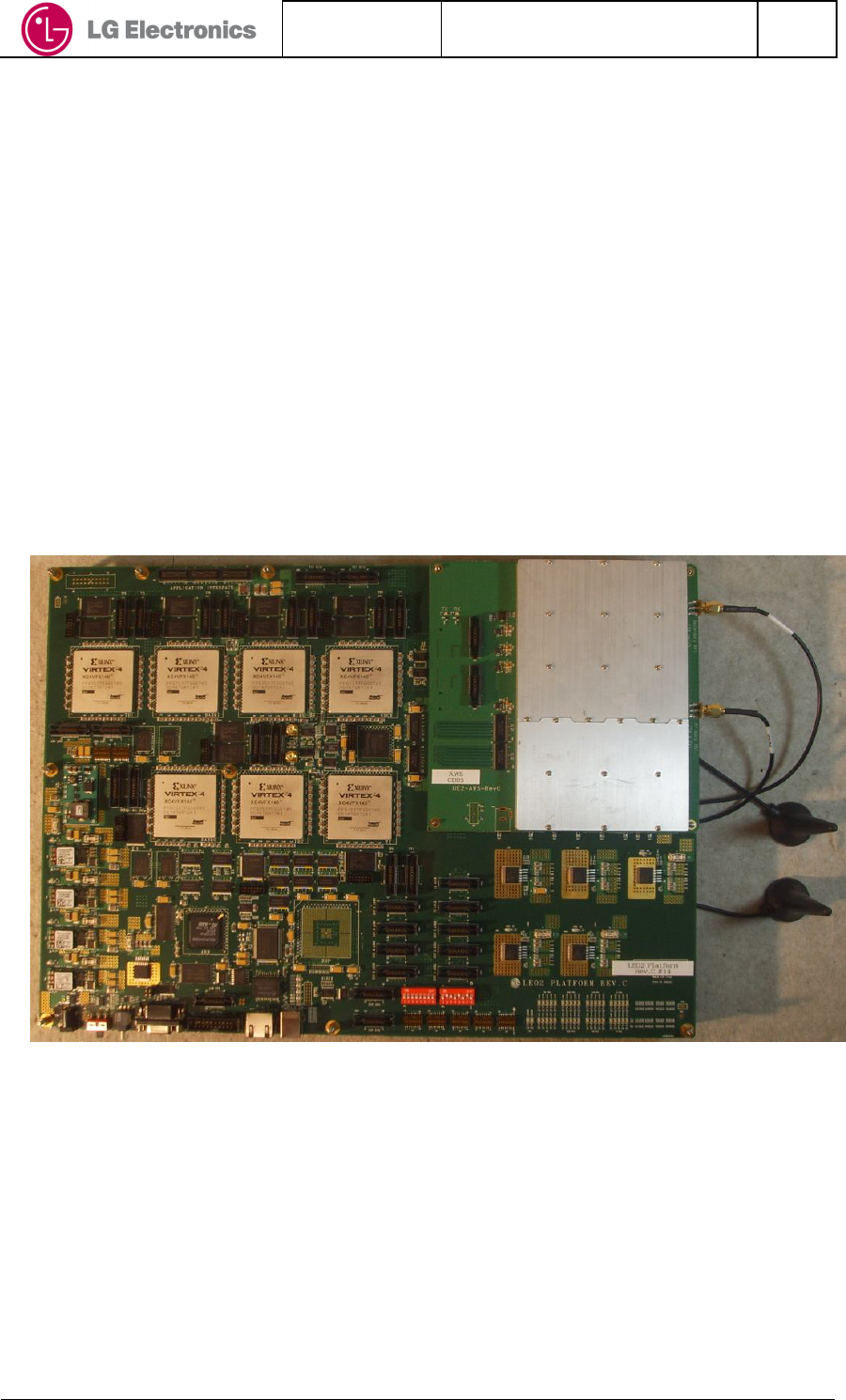
2.2 Photograph of the LEO2-B platform board 19
20
21
22
23
24
Figure 1. Photograph of LEO2-B platform 25
26
- Mechanical size of platform board is 420 (W) x 300 (H) mm 27
Updated
2008-09-08
File
LEO2 Platform Hardware Manual
Rev.
V1.0
LGE Proprietary 3 MCTR Lab.
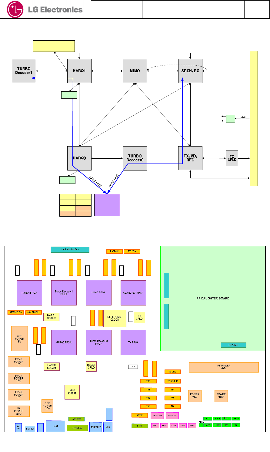
2.3 Top level block diagram 1
2
RX_FRAME_SYNC_N
OPT_CTLCH_SYMB[8]
OPT _CCH_STB, START, END
OPT_CCH_IDX[10]
RSVD[10]
32 Signals
54 Signals
CTLCH_SYMB[8]
CTLCH_STB, START, END
CTLCH_IDX[10]
OPT_RX_FRAME_SYNC_N
RSVD[32]
TX_FI LTER_OUT[48]
TX_FILTER_IQ_SEL
RSVD[10]
59 Signals
RF_GPIO[16]
4ch SPI
32 Signals
RX_FRAME_SYNC_N
RX_SUB_FRAME_SYNC_N
ENG_EN[5]
ORX_WR, ADDR[10], DATA[32]
MIMO_WR_ADDR[10], DATA[32]
SC_RD_DATA0[32]
SC_RD_DATA1[32]
SC_RD_STB, IDX[2]
SC_RD_EN, ADDR[11]
SC_RD_SYMB_IDX[2]
ORX_OPT[100]
RSVD[64]
310 Signals
32 Signals
32 Signals
51 Signals
51 Signals
149 Signals
149 Signals
100 Signals
Application Interface
EPI, NAND, USB
SDIO, SPI, DIP SW
96 Signals
OPT_DCH0_SYMB0[8]
OPT_DCH0_SYMB1[8]
OPT_DCH0_STB, START, END
RSVD[13]
OPT_DCH1_SYMB0[8]
OPT_DCH1_SYMB1[8]
OPT_DCH1_STB, START, END
RSVD[13]
DATACH0_SYMB0[8]
DATACH0_SYMB1[8]
DATACH0_STB, START, END
RSVD[ 32]
DATACH1_SYMB0[8]
DATACH1_SYMB1[8]
DATACH1_STB, START, END
RSVD[32]
TD0_START
TD0_IMEM_WE, SEL[3]
TD0_IMEM_WADDR[12]
TD0_IMEM_WDATA[64]
TD0_DB_DONE, DEC_DONE
HARQ0_START
HARQ0_PARAM_START
RSVD[64]
RSVD[100]
TX_I[12]
TX_Q[12]
RSVD[2]
26 Signals
RX0_I[ 12], RX0_Q[12]
RX1_I[ 12], RX1_Q[12]
48 Signals
PLL
30.72/61.44/122.88MHz
TurboDecoder_CLK
64bits
mDDR
ARM926EJ-S
64bits
mDDR
TD1_START
TD1_IMEM_WE, SEL[3]
TD1_IMEM_WADDR[12]
TD1_IMEM_WDATA[64]
TD1_DB_DONE, DEC_DONE
HARQ1_START
HARQ1_PARAM_START
RSVD[64]
SDRAM
USB
UART
ETM
NAND
Ethernet
Serial
Flash
JTAG
RF Daughter connector
3
Figure 2. Top level block diagram 4
5
6
2.4 Placement map 7
HARQ TP0
HARQ TP1
TD1 TP0
TD1 TP1
MIMO TP0
MIMO TP1
SRCH TP0
SRCH TP1
TX TP0
TX TP1
TD0 TP0
TD0 TP1
HARQ0 TP0
HARQ0 TP1
RF RX RF TX
RESET
ETHERNET
J1
J4
J7
J10
J11
J6
J3
8
Figure 3. Placement map of the LEO2-B 9
Updated
2008-09-08
File
LEO2 Platform Hardware Manual
Rev.
V1.0
LGE Proprietary 4 MCTR Lab.
1
3. Block description 2
3
3.1 FPGA subsystem 4
The LEO2-B Platform supports 7 FPGAs (xilinx virtex4 FX140, 1517pin package) for LTE UE 5
modem algorithm. Functionality of each FPGA is 6
- TX FPGA : Transmit block, Viterbi decoder, RF board control 7
- SRCH FPGA : Receiver block 8
- MISO FPGA : Receiver block and MISO 9
- HARQ 0/1 FPGA : Hybrid ARQ block 10
- Turbo Decoder 0/1 FPGA : Decoder block 11
12
Signal connection of FPGAs is 13
- ARM926 bus signal is connected to commonly all FPGAs, except MISO FPGA. 14
- 32 common reserved signals are connected commonly. 15
- 64 test signals of each FPGA are connected to MICTOR probing header. 16
- 4 GPIO LEDs of each FPGAs 17
- Detailed signals are described on block diagram. 18
19
FPGA configure bitstream is stored in platform flash. The maximum configuration bitstream size 20
of virtex4 FX140 is 47,856,896. Bitstream is stored in 2 serial daisy chained memories; capacity is 21
32Mb and 16Mb. Proper binary image should be fused on each platform memories. Xilinx 22
Platform cable connection for image fusing are J12 (TX FPGA), J10 (SRCH FPGA), J7 (MISO 23
FPGA), J3 (HARQ0 FPGA), J4 (HARQ1 FPGA), J6 (Turbo Decoder 0 FPGA) and J1 (Turbo 24
Decoder1 FPGA), which are placed beside of each FPGAs. 25
26
27
3.2 ARM subsystem 28
29
30
Figure 4. ARM processor block 31
32
Updated
2008-09-08
File
LEO2 Platform Hardware Manual
Rev.
V1.0
LGE Proprietary 5 MCTR Lab.
The ARM processor is used to control the LTE UE modem logic. The processor has 1
ARM926EJ-S core and peripheral controllers. 2
3
ARM Processor 4
- ARM926EJ-S core max. 333MHz, 16KB-I/D cache, configurable TMC-I/D size, MMU, 5
TLB, JTAG and ETM trace module (multiplexed interfaces). 6
- 32KByte Rom (code customizable) 8KByte common SRAM. 7
- High performance linked list 8 channels DMA. 8
- Ethernet MII, management interface 9
- USB2.0 High speed device 10
- Ext. memory interface : 16bit DDR1@200MHz 11
- Flash interface: 8bits NAND and Serial. 12
- 10 independent Timers with programmable prescaler. 13
- RTC - WDOG - SYSCTR - MISC internal control registers. 14
- JTAG (IEEE1149.1) interface. 15
- Current clock frequency setting : ARM Core 300MHz, Bus 150MHz, SDRAM 150MHz 16
17
Memory 18
The memory capacity and speed grade, that is on this board, are 19
- SDRAM : 512Mbits, 16bits data access, DDR @ 150MHz 20
- NAND Flash : 1Gbits, 8bits parallel, code stored. 21
- Serial Flash : 64Mbits, boot loader stored. 22
23
External Interface 24
The LEO2-B Platform supports external interface for diagnostic monitoring and user data 25
transfer. 26
- High speed USB2.0 27
- 100Mbps Ethernet 28
29
Interrupt 30
9 interrupt inputs are from interrupt handler in Turbo decoder0 FPGA. 31
32
33
34
3.3 Debugger Interface 35
The LEO2-B platform support debugging interface, JTAG and ETM, for ARM926 36
37
ARM926 core 38
- JTAG : CON12 39
- ETM9 : CON11 40
41
42
43
Updated
2008-09-08
File
LEO2 Platform Hardware Manual
Rev.
V1.0
LGE Proprietary 6 MCTR Lab.
1
3.4 RF Interface 2
3
4
Figure 5. RF interface on LEO2-B platform board 5
6
7
8
Figure 6. Block diagram of RF daughter board 9
10
Updated
2008-09-08
File
LEO2 Platform Hardware Manual
Rev.
V1.0
LGE Proprietary 7 MCTR Lab.
The LEO2-B Platform supports RF daughter board interface to verify and test LTE UE modem 1
algorithm. The baseband IQ signals are transmitted and received on FPGAs, Transmit part is on 2
TX FPGA and Receive part is on SRCH, MISO FPGA. The bit resolution of IQ signal is 12bits. 3
The sampling frequencies are 122.88MHz for DAC and 61.44MHz for ADC. The transmit signal 4
and sampling clock are delivered through LVDS, because of it’s over 100MHz data rate. 5
The RF control signals, GPIO and SPIs, are generated on TX FPGA. 6
7
RF daughter board consist in following blocks 8
- 2 antenna ports : 1 Tx and 2 Rx 9
- 14bits TX DAC, 14bits RX ADC 10
- TX synthesizer, RX synthesizer 11
- Modulator, Demodulator, VGA, 12
- Power amp, LNA and passive RF devices 13
- 3 x 120pin connector 14
15
16
3.5 Reference Clock 17
18
19
Figure 7. Block diagram of clock distribution 20
21
The 19.2MHz reference clock for LEO2-B platform board is supplied from TCXO in RF daughter 22
board. From this ref. clock, all needed clock source for LTE UE modem is synthesized by PLLs. 23
The PLLs generated clock frequencies 30.72, 61.44, 122.88MHz, and 32KHz. 24
All PLL output clocks are supplied to FPGAs and other blocks. The clock skews on each FPGA 25
input pad is very low <1nsec. 26
There is additional reference clock oscillator on LEO2-B platform board for without RF daughter 27
board test situations. This clock path selection is controlled by the 7pin on SW6. (‘1’ on-board, ‘0’ 28
RF daughter board oscillator) 29
30
Updated
2008-09-08
File
LEO2 Platform Hardware Manual
Rev.
V1.0
LGE Proprietary 8 MCTR Lab.
1
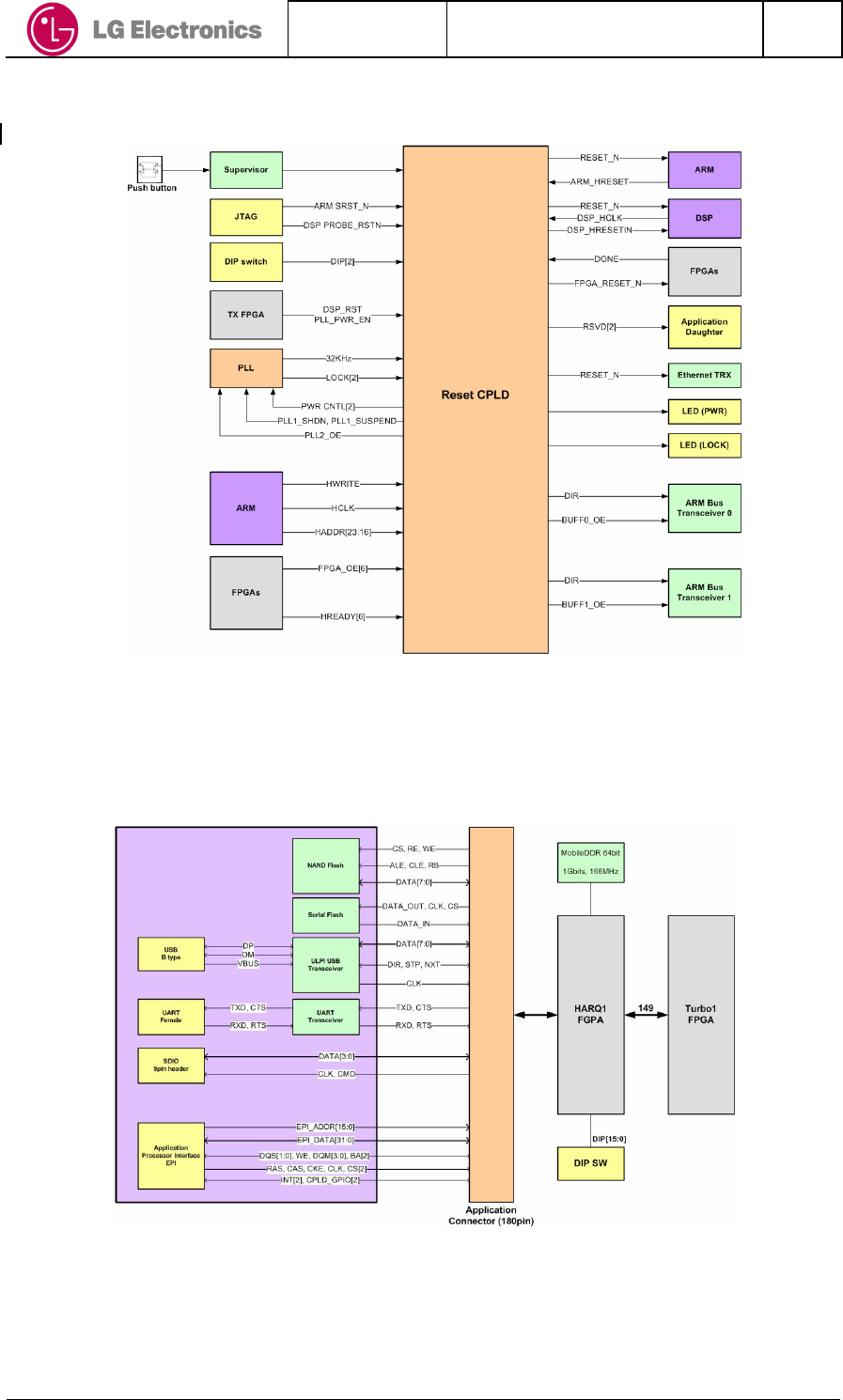
3.6 Reset 2
3
4
Figure 8. Block diagram of platform board reset scheme 5
6
The reset CPLD manages whole system reset scheme for ARM, Ethernet transceiver and each 7
FPGA reset. In the lower left lower corner of the platform board, a manual reset switch is provided. 8
9
10
3.7 Application interface 11
12
13
Figure 9. Block diagram of application interface 14
15
The LEO2-B platform supports a interface for external connection to application side. 3 kinds of 16
interfaces are supported, EPI, SDIO and USB. Application side will be designed as a platform 17
board at next phase.18
Updated
2008-09-08
File
LEO2 Platform Hardware Manual
Rev.
V1.0
LGE Proprietary 9 MCTR Lab.
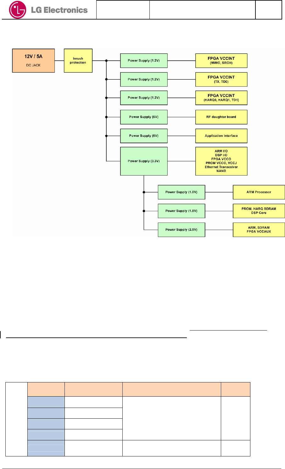
1
3.8 Power Supplies 2
3
4
Figure 10. Block diagram of power supplies 5
6
External power supplied from DC input jack on the platform board. To proper operation, 7
external AC to DC power supply should be 12V and >5A. All needed power sources of 8
platform board are supplied from DC-DC converters and LDOs devices. 9
10
11
4. DIP switch, LED and logic probing connector 12
13
4.1 ARM Processor debugging configuration switch setting 14
Two DIP switches (SW3, SW6) are used to ARM processor configurations and platform board 15
settings. Each control signals are assigned according to Table 1. “Switch on” represents “logic 16
low”, “switch off” represents “logic high” as other platform boards. 17
18
LEO2-B Platform default DIP switch settings are Table 1. 19
20
Remark: Setting the DIP switch in a wrong way may cause unexpected behavior that can 21
also damage the board since that all the production tests are intended to run in a different 22
environment. 23
Pin No. Name Description Default
1 ARM_INT(0)
2 ARM_INT(1)
3 ARM_INT(2)
4 ARM_INT(3)
ARM Processor interrupt input
"on" : assert interrupt
"off" : deassert interrupt
OFF
SW3
5 DIPSW_CPLD(0) Test signal input to reset CPLD
"on" : low signal to CPLD
"off" : high signal to CPLD
OFF
Updated
2008-09-08
File
LEO2 Platform Hardware Manual
Rev.
V1.0
LGE Proprietary 10 MCTR Lab.
1
Table 1. ARM processor setting DIP switches 2
3
4
5
4.2 General purpose LED indication 6
There are several LEDs are present on the board. Their meanings are described in Table 4-3. 7
LED turn on represent signal is high or status is good. 8
9
LED1 1.2V power OK LED2 1.2V power OK LED3 1.2V power OK
LED4 3.3V power OK LED5 DC IN OK LED6 1.0V power OK
LED7 Ethernet duplex LED8 Ethernet link 1000 LED9 Ethernet link 100
LED10
Ethernet link 10 LED11
Ethernet activity
LED13
2.5V power OK LED14
All FPGA done LED15
PLL Lock
LED16
Turbo Dec1 FPGA done LED17
ARM INT(4) LED18
TD1 GPIO(0)
LED19
ARM INT(5) LED20
TD1 GPIO(1) LED21
ARM INT(6)
LED22
TD1 GPIO(2) LED23
ARM INT(7) LED24
TD1 GPIO(3)
LED25
ARM INT(8) LED26
HARQ1 FPGA Done LED27
HARQ0 FPGA Done
LED28
HARQ1 GPIO(0) LED29
HARQ0 GPIO(0) LED30
HARQ1 GPIO(1)
LED31
HARQ0 GPIO(1) LED32
1.8V power OK LED33
HARQ1 GPIO(2)
LED34
HARQ0 GPIO(2) LED35
HARQ1 GPIO(3) LED36
HARQ0 GPIO(3)
LED37
MISO FPGA done LED38
TD0 FPGA Done LED39
MISO GPIO(0)
LED40
TD0 GPIO(0) LED41
MISO GPIO(1) LED42
TD0 GPIO(1)
LED43
MISO GPIO(2) LED44
TD0 GPIO(2) LED45
MISO GPIO(3)
LED46
TD0 GPIO(3) LED47
SRCH FPGA Done LED48
TX FPGA Done
6 DIPSW_CPLD(1) "off" : high signal to CPLD
7 SSP2_SS1
ARM processor booting device selection
'on' Boot from USB
'off' Boot NAND flash
OFF
8 SMI_WE
Write enable signal of serial flash
"on" : write protected
"off" : write enabled
OFF
Pin No. Name Description Default
1 ARM_TEST(0) OFF
2 ARM_TEST(1) ON
3 ARM_TEST(2) ON
4 ARM_TEST(3) OFF
5 ARM_TEST(4) ON
6 ARM_TEST(5)
ARM Processor configuration
OFF
7 CLK_SEL
Reference clock selection
'on' Reference clock from RF daughter
'off' on board reference clock
ON
SW6
8 OFF
Updated
2008-09-08
File
LEO2 Platform Hardware Manual
Rev.
V1.0
LGE Proprietary 11 MCTR Lab.
LED49
SRCH GPIO(0) LED50
TX GPIO(0) LED51
SRCH GPIO(1)
LED52
TX GPIO(1) LED53
SRCH GPIO(2) LED54
TX GPIO(2)
LED55
SRCH GPIO(3) LED56
TX GPIO(3) LED57
RF power OK
Table 2. LED signal mapping 1
2
3
4.3 Logic probing connector 4
5
All of the logic analyzer probing headers are MICTOR connector type, agilent E5346A logic 6
analyzer probing adaptor is needed to signal monitoring. Refer to LEO2-B schematic for detailed 7
signal mappings. 8
9
10
11
12
13
14
15
5 Description of Smart antenna and beam forming modes if applicable 16
17
1) SFBC(Space Frequency Block Code) mode : Transmit diversity mode 18
Easily speaking, SFBC which eNB sends same data through 2 antennas means 19
Tx diversity. 20
2) SM(Spatial multiplexing) mode 21
SM which eNB sends different data through 2 antennas helps high data 22
Rate. 23
24
Our LTE UE supports upper 2cases functionality. 25
That is, we support smart antenna and beam forming in wide meaning. 26
27
28
29
30
31
32
33
34
35
36
37
38
39
40
41
42
43
44
45
46
47
48
49
50
51
52
53
54
55
Updated
2008-09-08
File
LEO2 Platform Hardware Manual
Rev.
V1.0
LGE Proprietary 12 MCTR Lab.
6. Reference 1
[1]
2
3
4
Notice 5
6
OEM integrators and installers are instructed that the phrase. This device contains 7
8
Warning: Exposure to Radio Frequency Radiation The radiated output
power of this device is far below the FCC radio frequency exposure
limits. Nevertheless, the device should be used in such a manner that
the potential for human contact during normal operation is minimized.
In order to avoid the possibility of exceeding the FCC radio
frequency exposure limits, human proximity to the antenna should
not be less than 20cm during normal operation. The gain of the
antenna for 3GPP-Band4(1710~1755MHz) must not exceed -4 dBi.
The antenna(s) used for this transmitter must not be co-located or operating
in conjunction with any other antenna or transmitter.