LG Electronics USA LEO3 LTE User Equipment User Manual
LG Electronics USA LTE User Equipment Users Manual
Users Manual
Updated
File
UE RF Band4 HW Manual
Rev.
Written by
Reviewed by
Granted by
Managed by
Title
LEO3 RF (AWS) Hardware Manual
Type
Manual
LGE Proprietary i MCTR Lab.
ABSTRACT 1
This document is a hardware RF board manual for LTE user equipment platform. Contents of 2
this document are the description of each blocks and usage directions. It is recommended to 3
peruse this manual before operating RF Board. 4
5
HISTORY 6
Rev
Status
Date Author Contents
7
KEY WORDS 8
9
10
11
12
13
14
15
16
17
18
19
20
21
22
23
24
25
26
27
28
29
30
31
32
33
34
35
36
37
38
©Copyright, 2009 By LG Electronics Inc. All rights reserved.
No part of this document may be reproduced in any way, or by any means, without
the express written permission of LG Electronics Inc.
Mobile Communication Technology Research Lab.
533 Hogye-dong, Dongan-gu, Anyang-shi,
Kyongki-do, KOREA

Updated
File
UE RF Band4 HW Manual
Rev.
LGE Proprietary ii MCTR Lab.
1
2
3
4
5
6
7
8
9
10
11
12
13
14
15
16
17
18
19
20
21
22
23
24
25
26
27
28
29
30
31
32
33
34
35
36
37
38
39
40
41
42
43
[Notice] 44
1. The product described in this manual may be modified without prior notice for reliability, 45
functionality or design improvement. 46
2. Information contained in this manual is correct and reliable, but LG shall not be held 47
responsible for damage due to the use of information, product or circuit or infringement of 48
property rights or other rights. 49
3. This manual does not grant users the property rights and other rights of the third party or LG 50
Electronics Inc. 51
4. No part of this manual may be transcribed or duplicated without the written permission of LG 52
Electronics Inc. 53
5. The appearance of the product shown in this manual may slightly differ from that of the actual 54
product. 55

Updated
File
UE RF Band4 HW Manual
Rev.
LGE Proprietary iii MCTR Lab.
CONTENTS 1
1 Introduction................................................................................................................................ 1 2
1.1 Scope ..................................................................................................................................... 1 3
1.2 Terminology............................................................................................................................ 1 4
2 Features and Photograph........................................................................................................... 2 5
2.1 Features ................................................................................................................................. 2 6
2.2 Photograph of the LEO3 RF board.......................................................................................... 2 7
3 Block Diagram and Description.................................................................................................. 4 8
3.1 Block Diagram ........................................................................................................................ 4 9
3.2 Block Description .................................................................................................................... 4 10
3.2.1 RX Blocks .............................................................................................................................. 4 11
3.2.2 TX Blocks................................................................................................................................ 5 12
3.2.3 Common Blocks................................................................................................................. 6 13
4 Interface .................................................................................................................................... 7 14
4.1 Power supply .......................................................................................................................... 7 15
4.2 Digital I/Q Data & Sampling Cock ........................................................................................... 8 16
4.3 SPI ......................................................................................................................................... 8 17
4.4 Control signals (GPIO’s).......................................................................................................... 9 18
4.5 LEDs....................................................................................................................................... 9 19
4.6 Logic probing header .............................................................................................................. 9 20
5 Placement Map....................................................................................................................... 10 21
22
Updated
File
UE RF Band4 HW Manual
Rev.
LGE Proprietary iv MCTR Lab.
1
FIGURES 2
Figure 1: Photograph of LEO3 RF ................................................................................................... 3 3
Figure 2: RF Block Diagram (For RX/TX) ........................................................................................ 4 4
Figure 3: Diagrams of Power supply................................................................................................ 7 5
Figure 4: Diagrams of Data & Clock Signal Interface....................................................................... 8 6
Figure 5: Diagram of SPI interface .................................................................................................. 9 7
Figure 6: RX I/Q data probing Interface........................................................................................ 10 8
Figure 7: Top placement map of LEO3 RF (AWS) ....................................................................... 10 9
10
11
12
13
TABLES 14
Table 1: List of SPI programmable devices..................................................................................... 8 15
16
17

Updated
File
UE RF Band4 HW Manual
Rev.
LGE Proprietary 1
MCTR Lab.
1 Introduction 1
2
1.1 Scope 3
4
This RF board is intended for radio frequency part of LTE user equipment platform to develop 5
and verify LTE user equipment modem. This RF board is connected to 3rd version of LTE user 6
equipment platform (LEO3) as the form of daughter board. This document intends to describe the 7
brief architecture and usages of the board designed as RF part of LEO3 platform. 8
9
10
1.2 Terminology 11
12
ADC Analog to Digital Converter 13
AFC Automatic Frequency Compensation 14
DAC Digital to Analog Converter 15
LO Local Oscillator 16
LTE Long Term Evolution 17
LVDS Low-Voltage Differential Signaling 18
MISO Multi-In Single-Out 19
PA Power Amplifier 20
RF Radio Frequency 21
SAW Surface Acoustic Wave 22
UE User Equipment 23
VGA Variable Gain Amplifier 24

Updated
File
UE RF Band4 HW Manual
Rev.
LGE Proprietary 2
MCTR Lab.
1
2 Features and Photograph 2
3
2.1 Features 4
5
Supporting RF band: UMTS BAND-4(AWS) 6
Transmitting Frequency band: 1,710~1,755 MHz (45MHz) 7
Receiving Frequency band: 2,110~2,155 MHz (45MHz) 8
2-Receive path and 1-Transmit path (MISO) 9
+6V dc main power supply 10
19.2 MHz reference clock 11
Transceiver 12
Two chips transceiver solution by Infineon SMARTiLTE ICs(PMB_LTE_v093) 13
Triple-band operation 14
Three programmable LTE RF bandwidths: 5,10,20MHz 15
Supply voltage rage from 2.7 ~ 3.0V 16
Optional 2nd supply voltage from 1.71 ~ 3.0V 17
On-chip LDO 18
Different power-down modes 19
3-wire bus programmable 20
10-bit ADC and DAC support 21
61.44 MHz for AD conversion 22
122.88 MHz for DA conversion 23
Additional 16-bit HKDAC for Tx VGC and AFC 24
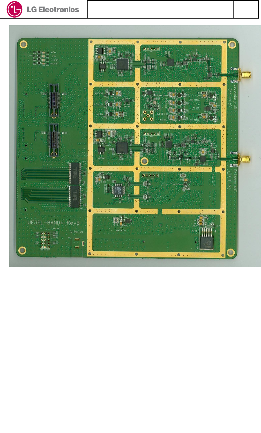
2.2 Photograph of the LEO3 RF board 25
26
Updated
File
UE RF Band4 HW Manual
Rev.
LGE Proprietary 3
MCTR Lab.
1
2
Figure 1: Photograph of LEO3 RF 3
4
- Mechanical size of board is 170 (W) X 170 (H) mm5
Updated
File
UE RF Band4 HW Manual
Rev.
LGE Proprietary 4
MCTR Lab.
1
3 Block Diagram and Description 2
3
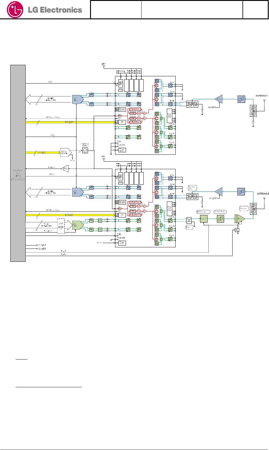
3.1 Block Diagram (AWS) 4
2.7-3.0V
2.7-3.0V
1.71-3.0V
1.4-1.6V
2.7-3.0V
2.7-3.0V
1.71-3.0V
1.4-1.6V
5
6
7
8
Figure 2: RF Block Diagram (For RX/TX) 9
10
3.2 Block Description 11
12
3.2.1 RX Blocks 13
14
Two receive paths, RX0 path and RX1 path, are designed for MISO technology to increase the 15
receiving data throughput. Both of receiving paths have the same structure and consist of the 16
following transceivers and anything else analog devices. 17
18
LNA 19
- This LNA is used for each receiving path 20
- LNA has the fixed 20dB gain at range of WCDMA Band4 21
22
Transceiver (Rx section) 23
- LNA2 with three programmable gain steps 24
- Complete analog baseband path without external components 25
- Three programmable baseband channel filter bandwidths 26
- Separate RX PGC 3-wire bus operation possible 27
- Performance 28
RX Total Gain : 2~80dB 29
Gain step: 1dB 30
Updated
File
UE RF Band4 HW Manual
Rev.
LGE Proprietary 5
MCTR Lab.
Gain switching time: under 6 us 1
LNA2 Gain: 0/-6/-12 dB 2
Gain deviation: +/-3 dB 3
NFDSB:12dB – 42dB 4
IP1dB: -15dBm 5
- Support frequency: 6
Band4: 2,110MHz ~ 2,155MHz 7
ADC 8
- Dual 10-bit, 150MSPS analog-to-digital converter 9
- 10-bit dedicated for each I/Q data 10
- A/D clock speed: 61.44MHz 11
- Two’s complement data formatting 12
- Internal fixed reference mode (the input span is 2 Vp-p) 13
14
RX LO 15
- RX PLL settling time: 320us (initial) 16
- RX PLL setting time: 150us (handover) 17
- VCO’s +frac-N PLL’s +loop filters on chip 18
- Receive PLL 19
The principle is exactly the same as for TX, but the frequency offset is now 20
1633iMHz (instead of 1404 MHz) for all bands but band VII, 21
Again the result is accommodated in a 13-bit word in the RX PLL Divider Register. 22
For band VII the offset is 2300 MHz. 23
24
25
3.2.2 TX Blocks 26
27
In transmit path, it is connected to a duplexer linked to ANT0. The transmitting data from LEO3 28
platform is the dedicated 12-bit digital signals for each I/Q via DAC. And its signaling uses LVDS 29
system for high speed data transmitting. Refer to the block diagram at section 2.3. The transmit 30
data pass through the following devices. 31
32
33
Level Translator 34
- High speed data level conversion, LVDS-to-CMOS 35
36
DAC 37
- Dual 10-bit, 125MSPS digital-to-analog converter 38
- 10-bit dedicated for each I/Q data 39
- D/A clock speed: 122.88MHz 40
- Offset binary data formatting 41
42
Transceiver (Tx section) 43
- RF VGA’s with >85dB gain range 44
- Three programmable baseband filter bandwidths 45
- Performance 46
POUTmax: 3~7dBm 47
POUTmin: -77dBm 48
TXGC range:0.5V ~ 2.2V 49
Gain switching time:10usec 50
NTX: -136dBm/Hz 51
Carrier suppression:26dB 52
- Support frequency: 53
Band4: 1,710MHz ~ 1,755MHz 54
55
Digital Attenuator 56
- Single 10 dB Step 57
- Control voltage: -8.5V≤Vc≤+8V 58
Updated
File
UE RF Band4 HW Manual
Rev.
LGE Proprietary 6
MCTR Lab.
- Low Loss: 0.3 dB @ 900 MHz 1
- Low Cost SOT-25 Package 2
3
Power Amplifier 4
- Operating frequency: 1,710 ~ 1,785MHz 5
- Max output power: 28.5dBm 6
7
TX LO 8
- TX PLL settling time: 325us(initial) 9
- TX PLL settling ime: 150us (Handover) 10
- VCO’s+frac-N PLL’s+loop filters on chip 11
For bands I, II, III, IV and IX the desired frequency is programmed by setting the distance, 12
in multiples of 100 kHz, from the fixed frequency offset of 1404 MHz. The result is 13
accommodated in a 13-bit word in the TX PLL Divider Register. 14
For bands V, VI and VIII, the programmed frequency must be twice the wanted frequency. 15
For Band VII the fixed offset is 2250 MHz. 16
17
18
19
3.2.3 Common Blocks 20
21
VCTCXO 22
- AFC supported by the external gain control voltage 23
- Generating reference clock for transceiver 1st and 2nd respectively 24
- Generating baseband clocks as the reference clock source 25
26
16-bit HKDAC for AFC and Tx VGC control 27
- Dual channel 16-bit DAC 28
- Programmable by 3 wire serial interface, SPI 29
- Its analog output voltage level functions the following: 30
1) AFC support 31
2) VGA gain control at transmit path 32
Updated
File
UE RF Band4 HW Manual
Rev.
LGE Proprietary 7
MCTR Lab.
1
4 Interface 2
3
The RF board for interfacing with LEO3 platform has 3 units of high speed 120pin connector. 4
One of them has the role for main power supply, 6V. The others make the interface between RF 5
to baseband (LEO3 platform) such as data transmitting and receiving, programming the SPI 6
device, transmitting control signals, supplying A/D or D/A clock, monitoring the status and etc. 7
8
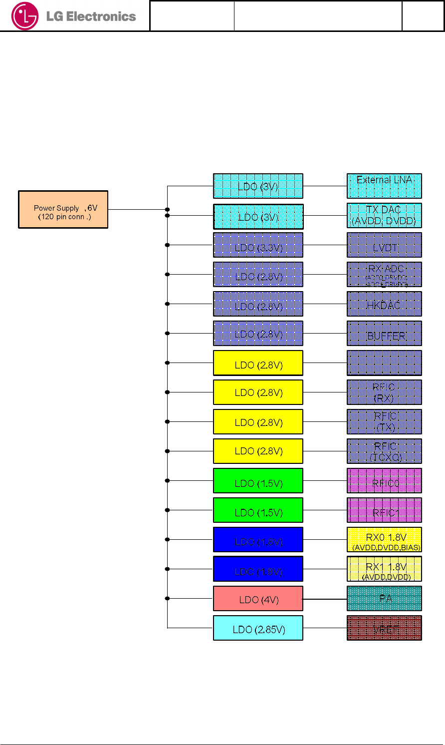
4.1 Power supply 9
10
11
12
13
Figure 3: Diagrams of Power supply 14
Updated
File
UE RF Band4 HW Manual
Rev.
LGE Proprietary 8
MCTR Lab.
1
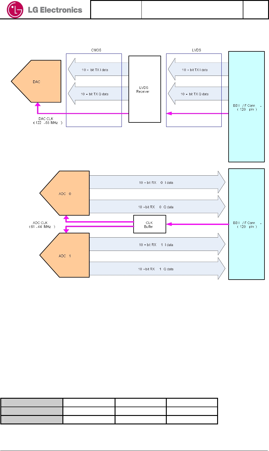
4.2 Digital I/Q Data & Sampling Cock 2
3
4
5
6
Figure 4: Diagrams of Data & Clock Signal Interface 7
8
9
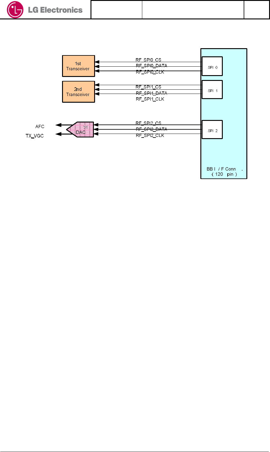
4.3 SPI 10
11
There are 3 programmable devices on RF board by using 3 wire SPI interface. 3 units SPI 12
blocks exist on the interface with baseband platform. They are listed at Table 1 (Also refer to 13
block diagram at Figure 5). 14
At this list, 1st transceiver and 2nd transceiver consist of each SPI0 and SPI1. Also 16-bit 15
HKDAC has the dedicated by SPI2. It can be possible by using a dedicated chip select signal for 16
each device with LLDM software. When selecting one of them, a dedicated chip select signal 17
enables its device to program. 18
19
20
21
22
23
24
25
Table 1: List of SPI programmable devices 26
SPI Device 1st Transceiver 2nd Transceiver 16bit-HKDAC
SPI block SPI0 SPI1 SPI2
SPI data bit - - 16
Updated
File
UE RF Band4 HW Manual
Rev.
LGE Proprietary 9
MCTR Lab.
1
2
3
4
5
Figure 5: Diagram of SPI interface 6
7
8
4.4 Control signals (GPIO’s) 9
10
For control the RF blocks, the control signals from LEO3 platform are connected as the below. 11
12
- BS(1)_IDLE: Enables the LDOs and LED for a self-Indicator 13
- TX_ON: Enables the LDOs at transmit path and transmit block at 1st Transceiver (Including 14
turns on LED for a self-indicator) 15
- PA_R0 : Controls the power mode of transmitter block (Including D-attenuator) 16
- PA_EN : Enables PA 17
- LNA_EN0: Enables the LNA of antenna0 path (At the 1st transceiver) 18
- LNA_EN1: Enables the LNA of antenna1 path (At the 2nd transceiver) 19
- TCXO_ON: Enables the LDO for source clock (VC-TCXO) 20
- GPIO_SLEEPB(0): Enables the 1st transceiver (Via Master on signal) 21
- GPIO_SLEEPB(1): Enables the 2nd transceiver (Via Master on signal) 22
23
24
4.5 LEDs 25
26
To indicate PLL lock status of 1st transceiver(LD_RFIC0) and 2nd transceiver(LD_RFIC1), two 27
LEDs (D401, D404) are present on the board. When locked at the frequency by setting the SPI 28
from LEO3, LD output of each Transceiver turns on this LED. 29
Anything else, there are two more LEDs(D4032 D403) for TX_ON and IDLE. 30
31
32
4.6 Logic probing header 33
34
The type of logic probing header is MICTOR connector. For each receive path, 20-bit 35
dedicated I/Q data is mapped to this (J408, J409). When using this logic probing, agilent E5346A 36
logic analyzer probing adaptor is needed to signal monitoring. The following figure is captured 37
from the schematic. 38
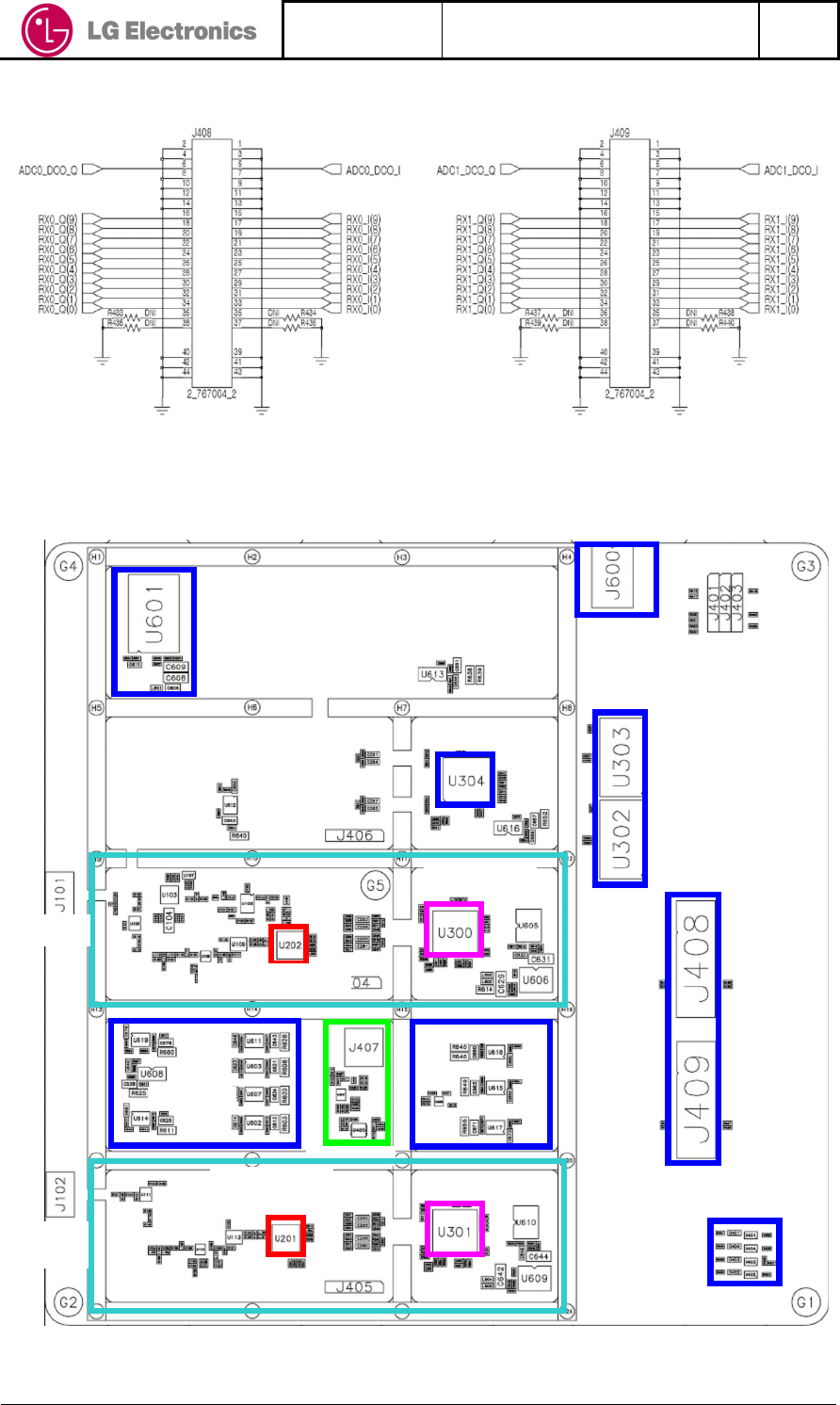
Updated
File
UE RF Band4 HW Manual
Rev.
LGE Proprietary 10
MCTR Lab.
1
2
3
Figure 6: RX I/Q data probing Interface 4
5 Placement Map 5
6
7
8
Figure 7: Top placement map of LEO3 RF (AWS) 9
First Transceiver
Second
Transceiver
10bit DAC
10bit ADC
10bit ADC
TCXO
Antenna0
Antenna1
L/T
DC
Jack
Probing
con.
LEDs
PAM
LDO
LDO
LDO
SPI Header
Updated
File
UE RF Band4 HW Manual
LGE Proprietary 11 MCTR Lab.
Notice 1
2
OEM integrators and installers are instructed that the phrase. This device contains 3
4
Warning: Exposure to Radio Frequency Radiation The radiated output
power of this device is far below the FCC radio frequency exposure
limits. Nevertheless, the device should be used in such a manner that
the potential for human contact during normal operation is minimized.
In order to avoid the possibility of exceeding the FCC radio
frequency exposure limits, human proximity to the antenna should
not be less than 20cm during normal operation. The gain of the
antenna for 3GPP-Band4(1710~1755MHz) must not exceed -4 dBi.
The antenna(s) used for this transmitter must not be co-located or operating
in conjunction with any other antenna or transmitter.