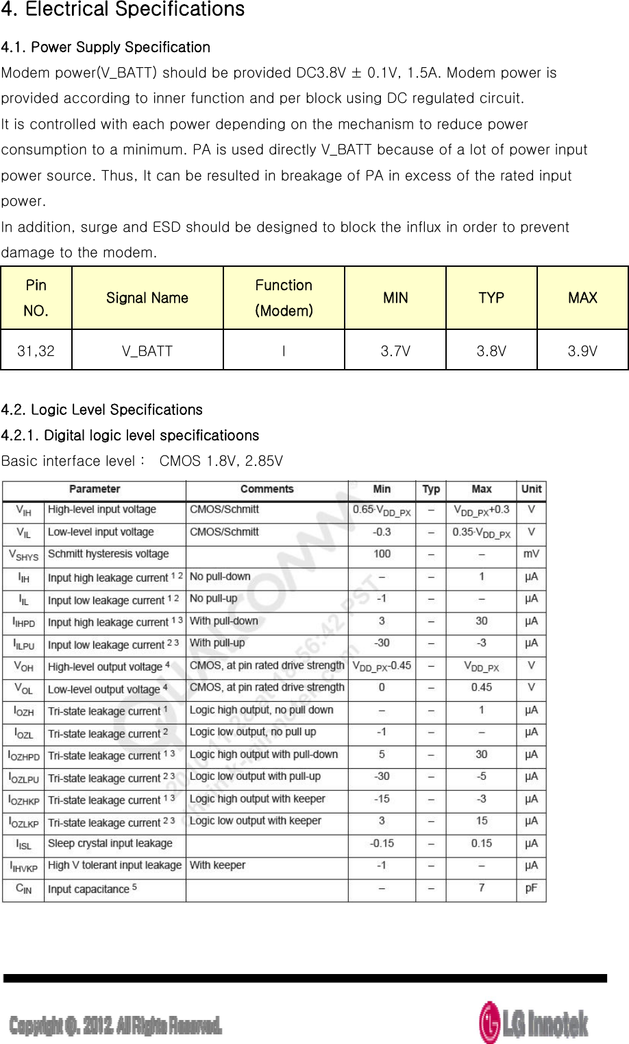
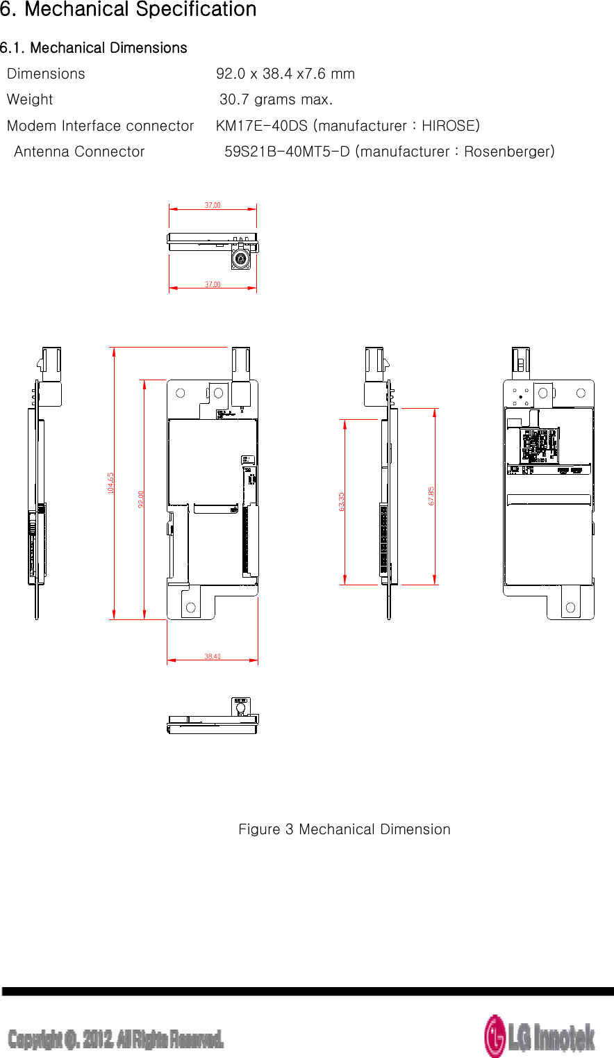
LG Innotek D660V Telematics Module User Manual LTD VH1000 User Manual 120611

LG Innotek Co., Ltd. Telematics Module LTD VH1000 User Manual 120611

User Manual

          PRODUCT : CDMA/EVDO WIRELESS MODEM  MODEL NAME : LTD-VH1000     1. Overview 2. Major    Features 3. Interface 4. Electrical Specifications 5. RF Specifications 6. Mechanical Specification 7. General Specification 8. Parts Map 9. Connector 10. Antenna Specification 11, RFx information
 1. Overview The LTD-VH1000 is achieved as  personal mobile communication devices of the compact radio equipment, the latest design of the parts becoming smaller, lighter weight having the 850/1900MHz bands. It is the vehicle’s telematics system that connect with CDMA(EVDO) wireless network and the wireless module with voice and  data  communication.  It  can  be  operated  at  land,  rivers,  and  other  similar areas. On EVDO operating mode, It can be communicated with uplink 1.8Mbps, downlink up to 3.1Mbps data  transfer speed  such as a movie or a video  call. It may be able to receive large amounts of data. Standard RS-232 port and USB port communicating with the host system via AT-command  or  control  commands  can  be  used  to  send  data.  Voice  calls  are possible  1.1. Product description The LTD-VH1000 module described in this manual is supported CDMA 1x (EVDO rev.A)    connectivity    to HYUNDAI TCU(Telecommunication control unit) This module is manufactured by LG INNOTEK and installed by HYUNDAI  1.2. Block diagram  Figure 1 Block Diagram
 2. Major    Features Mechanical Dimension    38.4 (W) x 92 (L) x 7.6 (T) mm  Interface    USB, UART, General Purpose I/O pins Antenna    FAKRA Connector Temperature *    Operation : -20℃ ~ +70 ℃    Storage : -40 ℃ ~ +85 ℃ CDMA   Main Chipset    MDM 6600 Memory    512Mb(NAND) / 256Mb(SDRAM) Standard    3GPP2 CDMA 1X, EVDO Rev.A                 - DL Speed : 3.1 Mbps - UL Speed : 1.8 Mbps Band    CDMA 850(DCN), 1900 (PCS)    GPS(Not supported)   Power    Max. 24dBm (Power Class 3) Etc. OS    Android 2.3 DC Power    3.8V Functions    Voice, Data, SMS
 2.1 Automotive Parts No  Item    Manufacturer    Operating Temperature/ Note   1    MDM6600   Qualcomm    -20~ 85℃   2    PAM    AVARGO    -30 ~ 85℃   3    Filter    EPCOS    -20∼+85°C   4    Quadplexer    AVARGO    -20∼+85°C   5    MEMORY(NAND)  NUMONYX  Automotive Part 6    MEMORY(SDRAM_DDR)  MICRON  Automotive Part 7    Capacitor / Inductor    Murata    Automotive Part 8    Resistor    YAGEO    Automotive Part 9    TCXO    KDS    Automotive Part 10  PCB    LGIT    6 Layer
 3. Interface   3.1. Pin outs Customer P/N is connected with outer device using 40 pin connectors   Figure 2 Modem Interface Connector Pin arrangement
 3.2. Pin Descriptions   NC Pin NO. Signal Name In/Out 기능 1, 2, 3, 4, 13, 15, 17, 38 NC     V_BATT 31, 32  POWER    POWER GND  21, 22, 33, 34, 40  GND    GND PCM 16  PCM_3.3V_TXD  O  PCM DATA OUT 18  PCM_3.3V_RXD  I  PCM DATA IN 19  PCM_3.3V_CLK  O  PCM CLK 20  PCM_3.3V_SYNC  O  PCM SYNC UART2 (DM Port) 37  TXD2  I  Serial Data Input 2 , HSDPA  디버깅 39  RXD2  O  Serial Data Output 2, HSDPA  디버깅 USB (USB2.0) 29  USB_VBUS  I  Power supply for the USB transceiver 35  USB_D+  I/O  USB differential data (+) 36  USB_D-  I/O  USB differential data (-) AUDIO (MIC/SPK) 23  MIC+  I  Differential Microphone input (+) 24  MIC-  I  Differential Microphone input (-) 25  SPK+  O  Analog Audio Differential Output (+) 26  SPK-  O  Analog Audio Differential Output (-) User Interface 9  SSl0  I  Air-bag    Signal input(Not use)   10  SSl1  I  CAN Wake Up Signal input (Not use)   11  BOOT_OK  O  Modem Booting Completion / Modem Wake Up  12  MSG  O  Received emergency message from Center 14  AUIDIO_ON-  O  Signified in voice communication(not use) 27  48H_END  O  Signified in 48 hours standby mode ending 28  RESET_IN-  I  Modem Hardware reset input 30  ACC(POWER_ON) I  Modem Power ON/ Modem POWER Sleep GPIO 5, 6, 7, 8, 9, 10, 14  GPIO  I/O  Possible to connect    to GPIO/  Table 1 Pin Descriptions
 3.3. UART ( RS-232 Interface ) This module is provided with interface supporting Standard RS-232 protocol. DCE(modem) is exchanged with data or control AT-Command through DTE(host). Pin NO. Signal Name Function (Modem) Pin Function Summary 37 TXD2 I Serial Data Input 2 39 RXD2 O Serial Data output 2  3.4. USB It is supported with universal serial bus for high data communication. It is satisfied with USB2.0 specification and supported with Max.480Mbps Pin NO. Signal Name Function (Modem) Pin Function Summary 29 USB_VBUS I Power supply for the USB transceiver 35 USB_D+ I/O USB differential data (+) 36 USB_D- I/O USB differential data (-)         3.5. AUDIO Modem is provided with condenser mic input, speaker output for voice call   Speaker output can connect with 32Ω speaker Pin NO.   Signal Name Function  (Modem) Pin Function Summary 23 MIC+ I Differential Microphone input (+) 24 MIC- I Differential Microphone input (-) 25 SPK+ O Analog Audio Differential Output(+) 26 SPK- O Analog Audio Differential Output (-)
 3.6. User Interface Signals Pin NO.   Signal Name Function (Modem) Pin Function Summary 9  GPIO    NC 10  GPIO    NC   11  BOOT_OK  O  Modem booting end / Modem Wake Up   12  MSG  O  Received emergency message from center 14  GPIO    NC 27  48H_END  O  Signified in 48 hours standby mode ending 28  RESET_IN-  I  Modem Hardware reset input 30  ACC(POWER_ON) I  Modem Power ON/Modem POWER Sleep  3.7. PCM Signals Pin NO.  Signal Name Function  (Modem) Pin Function Summary 16 PCM_3.3V_TXD    O PCM DATA OUT 18 PCM_3.3V_RXD I PCM DATA IN  19 PCM_3.3V_CLK O PCM CLOCK 20 PCM_3.3V_SYNC O PCM SYNC
 4. Electrical Specifications 4.1. Power Supply Specification Modem power(V_BATT) should be provided DC3.8V ± 0.1V, 1.5A. Modem power is provided according to inner function and per block using DC regulated circuit. It is controlled with each power depending on the mechanism to reduce power consumption to a minimum. PA is used directly V_BATT because of a lot of power input power source. Thus, It can be resulted in breakage of PA in excess of the rated input power. In addition, surge and ESD should be designed to block the influx in order to prevent damage to the modem.   Pin NO.   Signal Name Function  (Modem) MIN TYP MAX 31,32 V_BATT I 3.7V 3.8V 3.9V  4.2. Logic Level Specifications 4.2.1. Digital logic level specificatioons   Basic interface level :    CMOS 1.8V, 2.85V
 5. RF Specifications 5.1. Receiver  Bandwidth: 1.25MHz  Frequency: 869MHz  –  894MHz(BC0), 1930MHz – 1990MHz(BC1)  RF to Baseband Direct conversion(Zero IF)  Modulation method : QPSK,8PSK and 16QAM  Sensitivity: -104dBm under (BER = 0.5%under)     5.2. Transceiver  Frequency : 824MHz  –  849MHz(BC0), 1850MHz – 1910MHz(BC1)  Maximum RF Output: Power class3(BC0) Power class2(BC1), 23.01dBm ~ 30dBm max.  Modulation method: BPSK, QPSK AND 8PSK  Baseband to RF Direct conversion(Zero IF)
 6. Mechanical Specification 6.1. Mechanical Dimensions   Dimensions                                    92.0 x 38.4 x7.6 mm   Weight                                              30.7 grams max.   Modem Interface connector      KM17E-40DS (manufacturer : HIROSE)     Antenna Connector                      59S21B-40MT5-D (manufacturer : Rosenberger)      Figure 3 Mechanical Dimension
 6.2. Environmental Specifications   1) Storage Temp : -40℃ ~ +85℃   2) Operating Temp : -20℃ ~ +70℃         (-20℃ ~ +70℃ : 3GPP specifications satisfaction   -30℃~-20℃, +70℃~+80℃ : can be performance degradation   3) Operating humidity : 90% (50℃) relative humidity   4) Operating vibration : 5 Hz ~ 500 Hz Signe wave 1.5G
 7. General Specification 7.1. CDMA Electrical Specification                                                                                                 CH(850MHz/1900MHz)   시험  항목 Spec. CHANNEL 1017/25 358/563 774/1175 4.4.5 Maximum Output Power  23.01~30dBm       4.5.1 Conducted Spurious Emissions          885 kHz to 1.98 MHz    -42 dBc↓/30 kHz        1.98 MHz to 4.00 MHz    -54 dBc↓/30 kHz (BC0)    -50 dBc↓/30 kHz (BC1)      4.4.6 Minimum Controlled Output Power    -50dBm↓       4.3.4 Waveform Quality           Rho  0.94 ~1.00         Freq_E  +/-300.00Hz (BC0)    +/-150.00Hz(BC1)         Time_E  -1.00~1.00 us       4.4.9 Code Channel to Reverse Pilot Channel Output Power Accuracy           Data Rate: 9600 bps  3.5~4 dB       4.4.4 Range of Closed Loop Power Control             up @ Full rate  24↑         down @ Full Rate  -24↓         up @ Half rate  24↑         down @ Half Rate  -24↓         up @ Quarter rate  24↑         down @ Quarter Rate  -24↓         up @ Eighth rate  24↑         down @ Eighth Rate  -24↓       4.4.2 Time Response of Open Loop Control  PASS       4.4.1 Range of Open Loop Power           Open Loop Power Upper  -57.50~-38.50(BC0) -60.50~-41.50(BC1)         Open Loop Power Mid  -17.50~1.50(BC0) -20.50~-1.50(BC1)         Open Loop Power Sense  10.50~29.50(BC0) 10.50~29.50(BC1)       4.3.2 Reverse Pilot Channel to Code Channel Time Tolerance  ±10 ns.       4.3.3 Reverse Pilot Channel to Code Channel Phase Tolerance  0.05~0.15 deg       4.3.4 HWQ           Rho  0.94~1.00         Freq_E  +/-300.00Hz (BC0)    +/-150.00Hz(BC1)         Time_E  -1.00~1.00 us        3.5.1 Reference Sensitivity Level(-104/-25)  0.5%  ↓
 8.Parts Map                                                                         Top                                                                  Bottom
 9. Connector   9.1. Antenna Connector : 59S21B-40MT5_D(manufacturer : Rosenberger)
 9.2. 40Pin Connector : KM17E-40DS (manufacturer    : HIROSE)                                    Figure 4. 40 Pin connector
 10. Antenna Specification 10.1 Antenna spec. 10.1.1Frequency Band Frequency            Band                     CDMA 850  CDMA 1900 TX  824 ~ 849  1850 ~ 1910 RX  869 ~ 894  1930 ~ 1990  10.1.2    Normal value 50Ω  ±  Normal 10.1.3 Measuring method The impedance over the frequency bands shall be as close as possible to 50Ω  after matching. Both free space and talk position are considered. 10.2 VSWR The impedance matching should be optimized in the more critical talk position. 10.2.1 Maximum values in free space Band  CDMA 850  CDMA 1900 TX  RX  TX  RX VSWR  2.8  2  1.2  1.8 10.2.2   Measuring Method  Figure    5. Chamber
 a. Azimuth Pattern ; Co – pol    b. Azimuth Pattern ; Cross – pol    Figure    6. Gain Patterns
 11. RFx information The  RF  field  strength  of  the  wireless  module  or  modules  that  may  be embedded in your TCU is well all international RF exposure limits as known at  this  time.  Because  the wireless modules(which  may  be embedded  into your  TCU)  emit  less  energy  than  is  allowed  in  radio  frequency  safety standards  and  recommendations,  manufacturer  believes  these  modules   are safe for use. Regardless of the power levels, care should be taken to minimize human contact during normal operation. This  module  should  be  used  more  than  20cm(8  inches)  from  the  body when wireless devices are on and transmitting. This  transmitter  must  not  be  collocated  or  operate  in  conjunction  with any other antenna or transmitter. Operation is subject to the following two conditions: (1) this module may not cause interference , (2) this module must accept any interference that may cause undesired operation.  11.1 Information for integrator The integrator has to be aware not to provide information to the end user  regarding  how  to  install  or  remove  this  RF  module  in  the  user manual of the end product. The user manual which is provided by integrators for end users must include the following information in a prominent location. To comply with FCC RF exposure compliance requirements,       the antenna(W8E-MWC-20 Tri-band Dipole Antenna)     used  for  this  transmitter  must  be  installed  to  provide  a  separation distance  of  at  least  20cm  from  all  persons  and  must  not  be  co-located  or  operating  in  conjunction  with  any  other  antenna  or transmitter. Label for end product must include Contains FCC ID : YZP-D660V or A RF transmitter inside, FCC ID : YZP-D660V

Navigation menu