LG Innotek RBFAC21SA Class 2 Bluetooth Multimedia Module User Manual UserManual Rev 1
LG Innotek Co., Ltd. Class 2 Bluetooth Multimedia Module UserManual Rev 1
Installation Manual
OPERATION DESCRIPTION
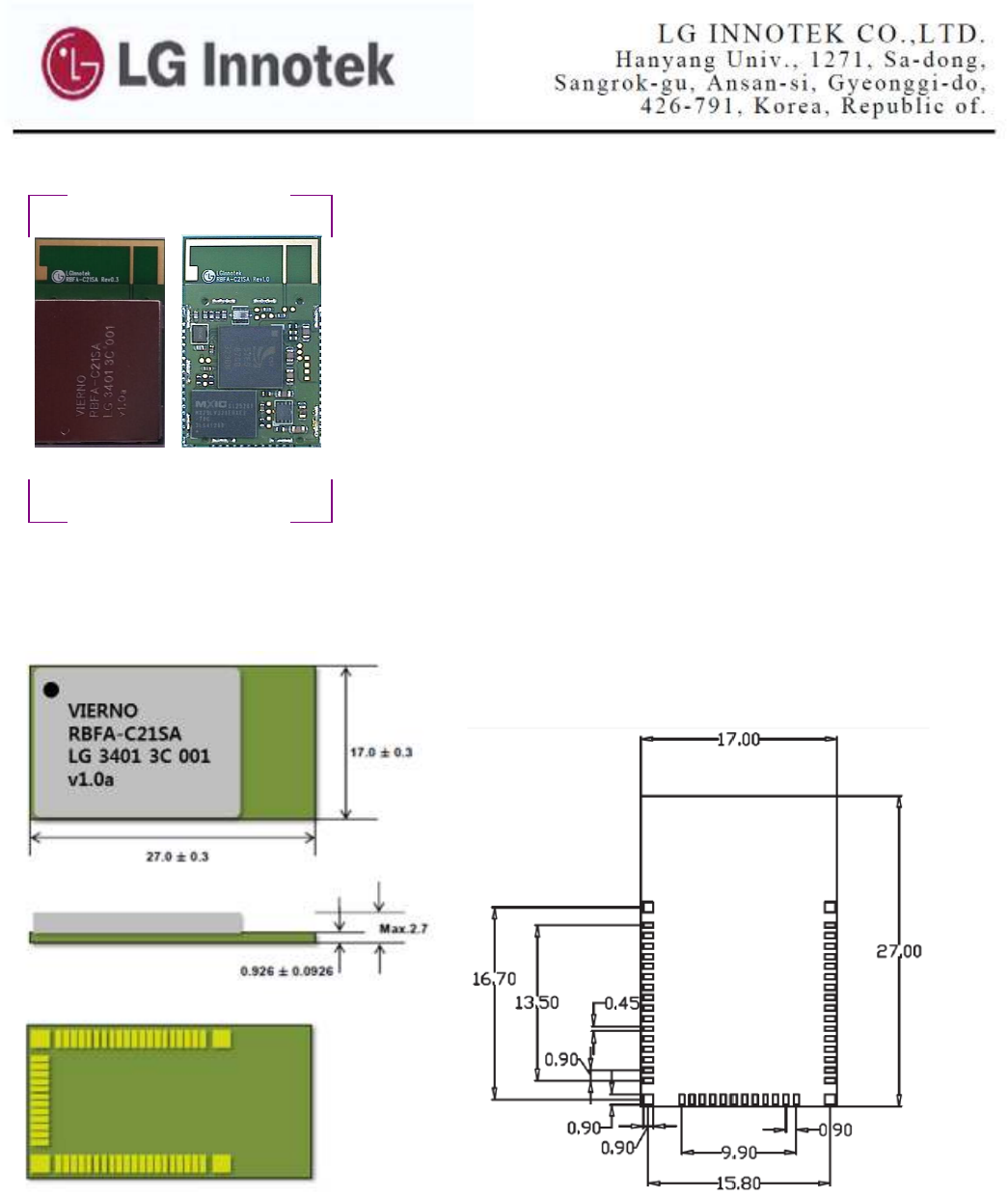
Model: RBFA-C21SA
FCC ID:
YZP-RBFAC21SA
Company LG INNOTEK CO.,LTD
Signature
Date 2014.10.06
Name J.S.SEO
Title Engineer
Description
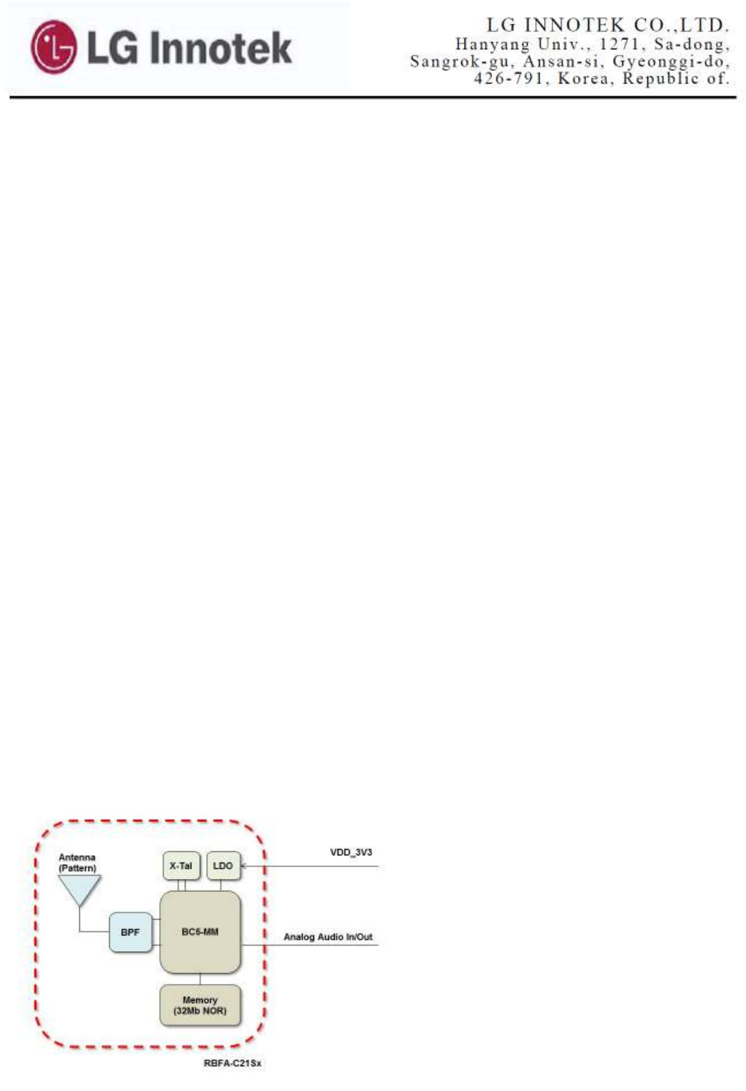
This product is applied to Class 2 Bluetooth Multimedia Module
RBFA-C21SA which includes the CSR BC5-MM chipset and
the integrated pattern antenna.
Features
- Sensitivity : Typ. -88dBm
- Output Power : Typ. +2dBm Class 2
- Temperature Range : -40℃ ~ +85℃
- Supply Voltage : VDD – 3.1V to 3.6V
- Interface : UART, USB
- Bluetooth Specification v3.0 with EDR Compliant
Applications
- Automotive
- Bluetooth automotive wireless gateways
Dimensions
• Product Information
* Power Supply Specification
The power of DC3.1V ~ 3.6V is should be supplied to the Bluetooth module power(VDD). The module supplies the
power to the each block depending on the function. Module input power in excess of the rated input power may cause
damage to the internal components. And the influx of Surge and ESD also may lead to the damage of the modem in
the vehicle. For the prevention of this, the module is necessary to design block the influx of Surge and ESD.
Pin No. Signal Name Function
(Module case) MIN TYP MAX
11 VDD_3V3 In 3.1V 3.3V 3.6V
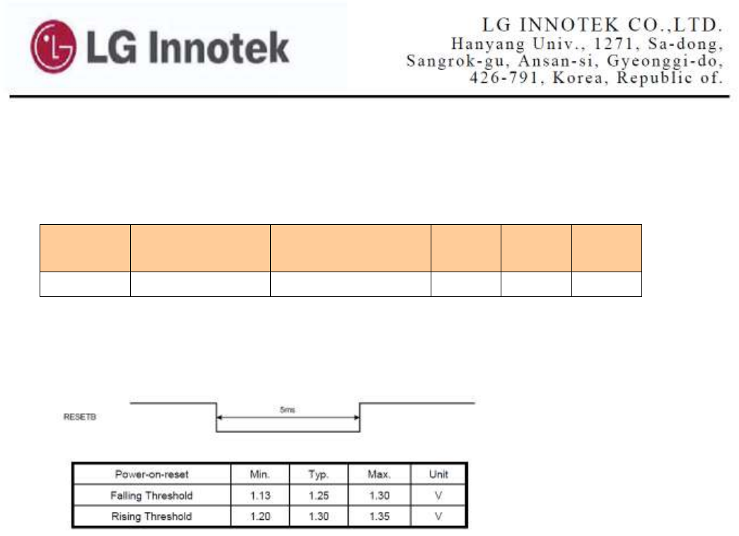
* RESET
The RESETB pin is an active low reset and is internally filtered using the internal low frequency clock oscillator. A
reset in performed between 1.5 and 4.0ms following RESETB being active. LGIT recommends that RESETB be
applied for a period greater than 5ms between the falling and the rising threshold voltage.
1) Bluetooth Module Features
• Bluetooth Power Class 2
• Embedded Fully Bluetooth v2.0/v2.1/v3.0 + EDR System Compliant
• Embedded Bluetooth Profile
• Embedded AEC/NR Algorithm for Handsfree
• Full-speed Bluetooth Operation with Full Piconet Support
• Operation Voltage is 3.3V Single Power Rail
• Excellent Compatibility with Cellular Telephones
• Command and data Interface is UART and USB
• 16-bit Internal Stereo CODEC
• Support for 802.11 Co-existence
• RoHS Compliant
2) Functionality Key Features : 2.1+EDR
• Secure simple pairing
• Sniff subrating
• Encryption pause resume
• Packet boundary flags
• Encryption
• Extended inquiry response
3) Functionality Key Features : 2.0+EDR
• AFH, including classifier
• Faster connection: enhanced inquiry scan (immediate FHS response)
• LMP improvements
• Parameter ranges
• AFH as master and automatic channel classification
• Fast connect: interlaced inquiry and page scan plus RSSI during inquiry
• eSCO, eV3 + CRC, eV4, eV5
• SCO handle
• Synchronization.
4) RBFA-C21SX Firmware Support Profile
-. A2DP1.2 with apt-X and AAC
-. AVRCP1.5(Controller)
General Features
Block Diagram
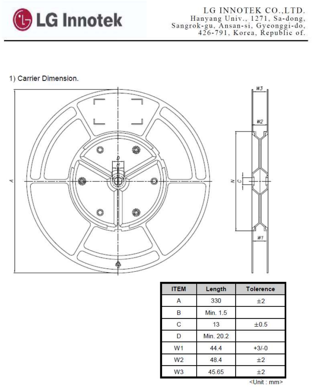
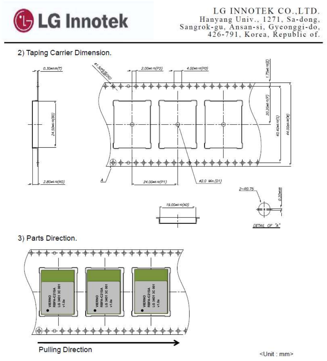
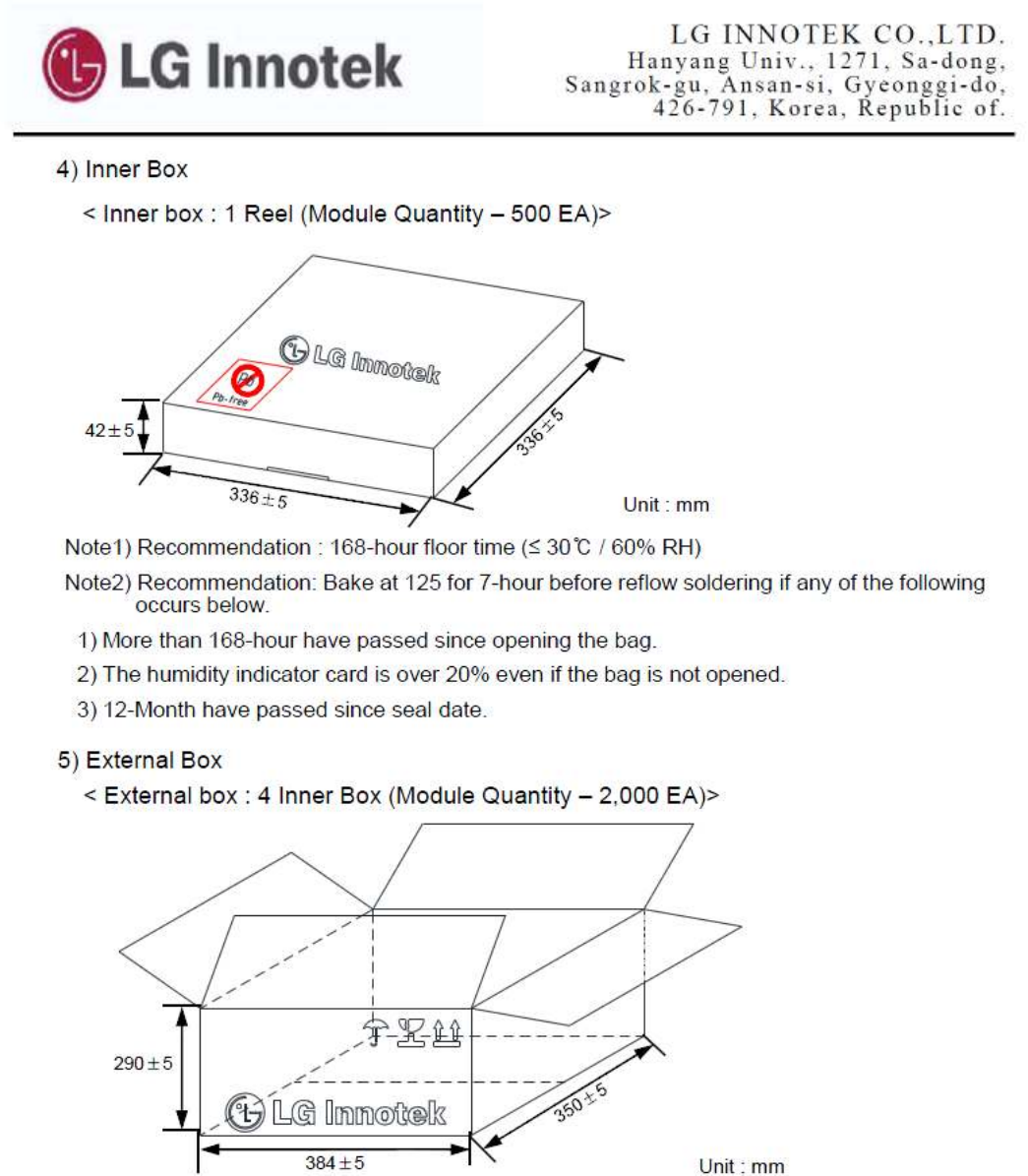
Packing Infomation

No.
Pin Name I/O
Pad Type Description
1 GND I - Ground
2 UART_RTS O Bidirectional CMOS output, tri-state,
with weak internal pull-up UART request to send active low
3 UART_CTS I
CMOS input with
weak internal pull
-
down UART clear to send active low
4 UART_Rx I
CMOS input with weak internal pull
-
down UART data input
5 UART_Tx O Bidirectional CMOS output, tri-state,
with weak internal pull-up
UART data output
- Recommended external 4.7kΩ
ΩΩ
Ω Pull-up
resistor.
6 PCM_IN I CMOS input, with weak internal pull-
down
Synchronous data input
-
The same pin as the I2S interface :
SD_IN
7 PCM_OUT O CMOS output, with weak internal
pull-down
Synchronous data output
-
The same pin as the I2S interfa
ce :
SD_OUT
8 PCM_SYNC
I/O
Bidirectional with weak internal pull-
down
Synchronous data Sync
- The same pin as the I2S interface : WS
9 PCM_CLK I/O
Bidirectional with weak internal pull-
down
Synchronous data clock
- The same pin as the I2S interface : SCK
10 RESET# I CMOS input with weak internal pull-
up
Reset if low. Input debounced so must be
low for >5ms to cause a reset
Recommended external 4.7kΩ
ΩΩ
Ω Pull-up
resistor & stability capacitor
11 VDD_3V3 I VDD Positive supply for Module
- Supply voltage : Typical 3.3V.
12 GND I - Ground
13 SPI_MISO O CMOS output, tristate, with weak
internal pull-down
SPI data output
- Used to program and configure (PS
Keys), and debug the BC5-MM
14 SPI_CSB I/O
Input with weak internal pull-up
Chip select for SPI, active low
- Used to program and configure (PS
Keys), and debug the BC5-MM
15 SPI_CLK I/O
Input with weak internal pull-down
SPI clock
- Used to program and configure (PS
Keys), and debug the BC5-MM
16 SPI_MOSI I CMOS input, with weak internal pull-
down
SPI data input
- Used to program and configure (PS
Keys), and debug the BC5-MM
17 LED[1] O - LED
18 LED[0] O - LED
19 GND I - Ground
20 AGND - - Analog Ground
21 MIC_A_P I Analog Microphone input positive, left
22 MIC_A_N I Analog
Microphone input negative, left
- Must be use external ESD protection
PIN Descriptions
No.
Pin Name I/O
Pad Type Description
23 Reserved
24 AGND - - Analog Ground
25 SPK_B_N O Analog Speaker output negative, right
26 SPK_B_P O Analog Speaker output positive, right
27 SPK_A_N O Analog Speaker output negative, left
28 SPK_A_P O Analog Speaker output positive, left
29 GND I - Ground
30 GND I - Ground
31 AIO[0] I/O
- TBD
32 PIO[0] I/O
- TBD
33 PIO[1] I/O
- TBD
34 PIO[2] I/O
- TBD
35 PIO[3] I/O
- TBD
36 USB_DN I/O
- USB data minus
37 USB_DP I/O
- USB data plus with selectable internal
1.5kΩ Pull-up resistor
38 GND I - Ground
39 PIO[10] I/O
- TBD
40 PIO[11] I/O
- TBD
41 PIO[9] I/O
- TBD
42 PIO[15] I/O
- TBD
43 PIO[12] I/O
- TBD
44 PIO[13] I/O
- TBD
45 GND I - Ground
46 GND I - Ground
47 GND I - Ground
48 GND I - Ground

FCC Information
This device complies with part 15 of the FCC Results. Operation is subject to the following two
conditions :
(1) This device may not cause harmful interface, and
(2) This device must accept any interference received, including interference that
may cause undesired operation.
Note: This equipment has been tested and found to comply with the limits for CLASS B digital device, pursuant to Part 15 of
FCC Rules. These limits are designed to provide reasonable protection against harmful interference when the equipment is
operated in a commercial environment This equipment generates, uses and can radiate radio frequency energy and, if not
installed and used in accordance with the instructions, may cause harmful interference to radio communications. However,
there is no guarantee that interference will not occur in a particular installation. If this equipment does cause harmful
interference to radio or television reception, which can be determined by turning the equipment off and on, the user is
encouraged to try correct the interference by one or more of the following measures:
1.1. Reorient or relocate the receiving antenna.
1.2. Increase the separation between the equipment and receiver.
1.3. Connect the equipment into an outlet on a circuit different from that to which receiver is connected.
1.4. Consult the dealer or experienced radio/TV technician for help.
WARNING
Changes or modifications not expressly approved by the manufacturer could void the user’s authority
to operate the equipment.

Information for OEM Integrator
This device is intended only for OEM integrators under the following conditions:
1) The antenna must be installed such that 20 cm is maintained between the antenna and users, and
2) The transmitter module may not be co-located with any other transmitter or antenna.
End product labelling
The label for end product must include “Contains FCC ID: YZP-RBFAC21SA”.
“CAUTION :
Exposure to Radio Frequency Radiation.
This equipment complies with FCC radiation exposure limits set forth for an uncontrolled environment. This equipment must
be installed and operated with minimum distance of 20cm between the radiator and your body. This transmitter module is
authorized only for use in device where the antenna may be installed such that 20 cm may be maintained between the
antenna and users.”