LG Innotek RBFAC21XX Bluetooth Complete Module User Manual r
LG Innotek Co., Ltd. Bluetooth Complete Module r
User Manual_r
LG Innotek Co, Ltd
PART NO. NAME MATERIAL SPEC FINISH SIZE
UNIT SCALE
DRAW DSGD CHKD APPD TITLE
DOCUMENT NO.
NO. Changes APPD
1. 0. `13.10.10
Initialize
RBFA-C217/8/9A(1-2)
User Manual(1/5)
B
H
Choi
I
P
Park
K
S
Kim
Description
This product is applied to Class 2 Bluetooth Multimedia Module
RBFA-C217/8/9A which includes the CSR BC5-MM chipset
and the integrated pattern antenna.
Features
- Sensitivity : Typ. -88dBm
- Output Power : Typ. +2dBm Class 2
- Temperature Range : -40℃ ~ +85℃
- Supply Voltage : VDD – 3.1V to 3.6V
- Interface : UART, USB
- Audio Interface : Analog In/Out, Digital In/Out(I2S)
- Bluetooth Specification v3.0 with EDR Compliant
Applications
- Handsfree
- Bluetooth automotive wireless gateways
Dimensions
• Product Information
LG Innotek Co, Ltd
PART NO. NAME MATERIAL SPEC FINISH SIZE
UNIT SCALE
DRAW DSGD CHKD APPD TITLE
DOCUMENT NO.
NO. Changes APPD
1. 0. `13.10.10
Initialize
RBFA-C217/8/9A(1-2)
User Manual(2/5)
B
H
Choi
I
P
Park
K
S
Kim
* Power Supply Specification
The power of DC3.1V ~ 3.6V is should be supplied to the Bluetooth module power(VDD). The
module supplies the power to the each block depending on the function. Module input power in
excess of the rated input power may cause damage to the internal components. And the influx of
Surge and ESD also may lead to the damage of the modem in the vehicle. For the prevention of this,
the module is necessary to design block the infloux of Sugre and EDS.
Pin NO. Signal Name Function
(Module case) MIN TYP MAX
13.14 VDD In 3.1V 3.3V 3.6V
*Memory Interface
①Memory Management Unit
The MMU provides a number of dynamically allocated ring buffers that hold the data that is in transit
between the host, the air or the Kalimba DSP. The dynamic allocation of memory ensures efficient
use of the available RAM and is performed by a hardware MMU to minimise the overheads on the
processor during data/voice transfers.
②System RAM
48Kbyte of on-chip RAM supports the RISC MCU and is shared between the ring buffers used to
hold voice/data for each active connection and the general-purpose memory required by the
Bluetooth stack.
③Kalimba DSP RAM
Additional on-chip RAM is provided to support the Kalimba DSP:
■16K x 24-bit for data memory 1 (DM1)
■12K x 24-bit for data memory 2 (DM2)
■6K x 32-bit for program memory (PM)
Parameter Value
Baud rate 115,200 baud
Flow control None
Parity None
Number of stop bits 1
Bits per byte 8
* UART Interface
RBFA-C21XX UART interface provides a simple mechanism for communicating with other serial
devices using the RS232 protocol. UART configuration parameters, such as baud rate and packet
format, are set using LGIT firmware.
LG Innotek Co, Ltd
PART NO. NAME MATERIAL SPEC FINISH SIZE
UNIT SCALE
DRAW DSGD CHKD APPD TITLE
DOCUMENT NO.
NO. Changes APPD
1. 0. `13.10.10
Initialize
RBFA-C217/8/9A(1-2)
User Manual(3/5)
B
H
Choi
I
P
Park
K
S
Kim
1) Bluetooth Module Features
• Bluetooth Power Class 2
• Embedded Fully Bluetooth v2.0/v2.1 + EDR System Compliant
• Embedded Bluetooth Profile
• Embedded AEC/NR Algorithm for Handsfree
• Full-speed Bluetooth Operation with Full Piconet Support
• Operation Voltage is 3.3V Single Power Rail
• Excellent Compatibility with Cellular Telephones
• Command and data Interface is UART and USB
• 16-bit Internal Stereo CODEC
• Support for 802.11 Co-existence
•RoHS Compliant
2) Functionality Key Features : 2.1+EDR
• Secure simple pairing
• Sniff subrating
• Encryption pause resume
• Packet boundary flags
• Encryption
• Extended inquiry response
3) Functionality Key Features : 2.0+EDR
• AFH, including classifier
• Faster connection: enhanced inquiry scan (immediate FHS response)
• LMP improvements
• Parameter ranges
• AFH as master and automatic channel classification
• Fast connect: interlaced inquiry and page scan plus RSSI during inquiry
•eSCO, eV3 + CRC, eV4, eV5
• SCO handle
•Synchronization.
4) RBFA-C21xxFirmware Support Profile
-. HFP1.6
-. AVRCP1.4
-. SPP1.1
-. GAP
-. OPP
-. PBAP1.0
-. GAVDP1.3
-. HID
-. MAP1.0
-. PAN(USER)
General Features
LG Innotek Co, Ltd
PART NO. NAME MATERIAL SPEC FINISH SIZE
UNIT SCALE
DRAW DSGD CHKD APPD TITLE
DOCUMENT NO.
NO. Changes APPD
1. 0. `13.10.10
Initialize
RBFA-C217/8/9A(1-2)
User Manual(4/5)
B
H
Choi
I
P
Park
K
S
Kim
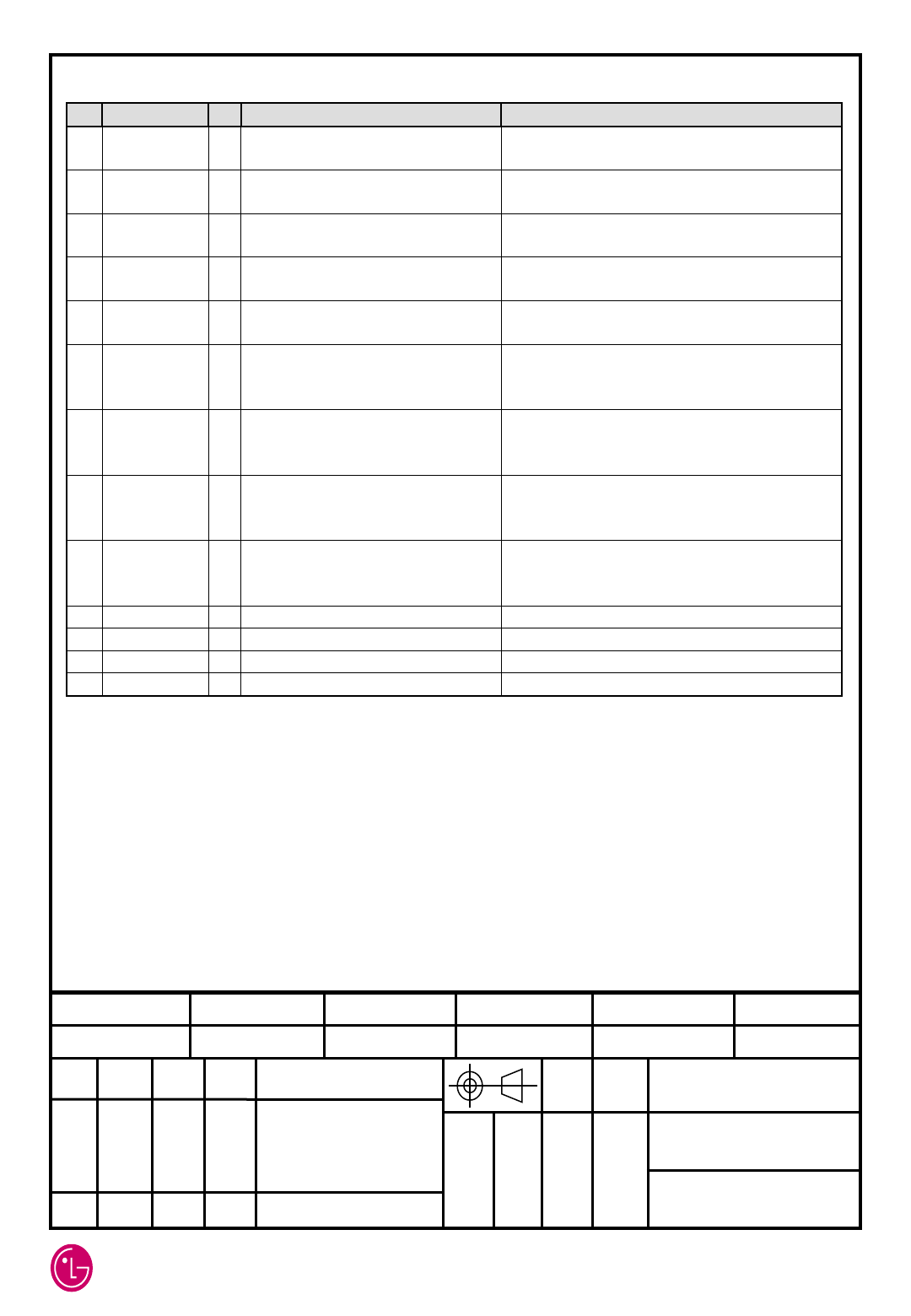
PIN Descriptions
No.
Pin Name
I/O
Pad Type Description
1 UART_Tx O
Bidirectional CMOS output, tristate,
with weak internal pull
-up
UART data output
-
Recommended external 4.7kΩ Pull-
up resisto
r.
2 UART_Rx I
CMOS input with weak internal pull
-down
UART data input
3 UART_RTS
O
Bidirectional CMOS output, tristate,
with weak internal pull
-up
UART request to send active low
4 UART_CTS
I
CMOS input with weak internal pull
-down
UART clear to send active low
5 GND - -
Ground
6 RESET# I
CMOS input with weak internal pull
-up
Reset if low. Input debounced so must be low
for >5ms to cause a reset
Recommended external 4.7k
Ω Pull-
up resistor
& stability capacitor
7 GND - -
Ground
8 VDD_3V3 I
VDD
Positive supply for Module
-
Supply voltage : Typical 3.3V.
9 RESERVED
- -
TBD
10
RESERVED
- -
TBD
11
Internal MIC B
ias -
Analog
Internal microphone bias
12
GND - -
Ground
13
AGND - -
Analog Ground
14
MIC_A_P I
Analog
Microphone input positive, left
15
MIC_A_N I
Analog
Microphone input negative, left
-
Must be use external ESD protection
16
AGND - -
Analog Ground
17
SPK_B_N O
Analog
Speaker output
negative, right
18
SPK_B_P O
Analog
Speaker output positive, right
19
SPK_A_N O
Analog
Speaker output negative, left
20
SPK_A_P O
Analog
Speaker output positive, left
21
GND - -
Ground
22
GND - -
Ground
23
GND - -
Ground
LG Innotek Co, Ltd
PART NO. NAME MATERIAL SPEC FINISH SIZE
UNIT SCALE
DRAW DSGD CHKD APPD TITLE
DOCUMENT NO.
NO. Changes APPD
1. 0. `13.10.10
Initialize
RBFA-C217/8/9A(1-2)
User Manual(5/5)
B
H
Choi
I
P
Park
K
S
Kim
PIN Descriptions
No.
Pin Name
I/O
Pad Type Description
24
PCM_IN I
CMOS input, with weak internal pull
-down
Synchronous data input
-
The same pin as the I2S interface : SD_IN
25
PCM_OUT O
CMOS output, with weak internal p
ull
-down
Synchronous data output
-
The same pin as the I2S interface : SD_OUT
26
PCM_SYNC
I/O
Bidirectional with weak internal pul
l-
down
Synchronous data Sync
-
The same pin as the I2S interface : WS
27
PCM_CLK
I/O
Bidirectional with weak internal pul
l-
down
Synchronous data clock
-
The same pin as the I2S interface : SCK
28
EC/NR Logger
O
Bidirectional with programmable st
rength internal pull
-up/down
Programmable input/output line
-
Using the AEC/NR data logger
29
SPI_MISO O
CMOS output, tristate, with weak in
ternal pull
-down
SPI data output
- Used to program and configure (PS Keys), an
d debug the BC5
-MM
30
SPI_MOSI I
CMOS input, with weak internal pull
-down
SPI data input
- Used to program and configure (PS Keys), an
d debug the BC5
-MM
31
SPI_CSB
I/O
Input with weak internal pull
-up
Chip select for SPI, active low
- Used to program and configure (PS Keys), an
d debug the BC5
-MM
32
SPI_CLK
I/O
Input with weak internal pull
-down
SPI clock
- Used to program and configure (PS Keys), an
d debug the BC5
-MM
33
GND - -
Ground
34
GND - -
Ground
35
GND - -
Ground
36
GND - -
Ground
FCC Statement
FCC Part 15.19
This device complies with part 15 of the FCC Rules. Operation is subject to the following
two conditions: (1) This device may not cause harmful interference, and (2) this device
must accept any interference received, including interference that may cause undesired
operation
FCC Part 15.21
Any changes or modifications (including the antennas) to this device that are not expressly
approved by the manufacturer may void the user's authority to operate the equipment.
Part 15.105 (B)
Note : This equipment has been tested and found to comply with the limits for a Class B digital
device, pursuant to part 15 of the FCC Rules. These limits are designed to provide reasonable
protection against harmful interference in a residential installation This equipment generates,
uses and can radiate radio frequency energy and, if not installed and used in accordance with
the instructions, may cause harmful interference to radio communications, However, there is
no guarantee that interference will not occur in a particular installation. If this equipment does
cause harmful interference to radio or television reception, which can be determined by turning
the equipment off and on, the user is encouraged to try to correct the interference by one or
more of the following measures:
- Reorient or relocate the receiving antenna.
- Increase the separation between the equipment and receiver.
- Connect the equipment into an outlet on a circuit different from that to which the
receiver is connected.
- Consult the dealer or an experienced radio/TV technician for help.
Modifications not expressly approved by the manufacturer could void your authority to
operate the equipment under FCC rules.
RSS-GEN 7.1.3 User manual Notice for Licence-Exempt Radio Appartus.
This device complies with Industry Canada licence-exempt RSS standard(s). Operation is
subject to the following two conditions: (1) this device may not cause interference, and (2)
this device must accept any interference, including interference that may cause undesired
operation of the device.
L'exploitation est autoris e aux deux conditions suivantes : (1) l'appareil ne doit pas produire
de brouillage, et (2) l'utilisateur de l'appareil doit accepter tout brouillage radio lectrique subi,
m me si le brouillage est susceptible d'en compromettre le fonctionnement.
RF Exposure Statement (2.1091)
FCC RF Radiation Exposure Statement: FCC RF Radiation Exposure Statement: This
equipment complies with FCC RF Radiation exposure limits set forth for an uncontrolled
environment. This device and its antenna must not be co-located or operating in conjunction
with any other antenna or transmitter.
This equipment should be installed and operated with a minimum distance of 20cm between
the radiator and your body.
RF du FCC d'exposition aux radiations: Cet équipement est conforme à l'exposition de la FCC
rayonnements RF limites établies pour un environnement non contrôlé. L’antenne pour ce
transmetteur ne doit pas être même endroit avec d’autres émetteurs sauf conformément à la
FCC procédures de produits Multi-émetteur.
Cet équipement doit être installé et utilisé avec une distance minimale de 20cm entre le
radiateur et votre corps.
* Information for OEM integrator
The OEM integrator has to be aware not to provide information to the end user regarding how
to install or remove this RF module in the user manual of the end product.
The user manual which is provided by OEM integrators for end users must include the
following information in a prominent location.
“To comply with FCC RF exposure compliance requirements, the antenna used for this
transmitter must be installed to provide a separation distance of at least 20 cm from all persons
and must not be co-located or operating in conjunction with any other antenna or transmitter.”
Label for end product must include “Contains FCC ID: YZPRBFAC21XX, IC: 7414A-
RBFAC21XX" or “ A RF transmitter inside, FCC ID: YZPRBFAC21XX, IC: 7414A-
RBFAC21XX”.
* Information pour les OEM intégrateur
L'intégrateur OEM doit être conscient de ne pas fournir des informations à l'utilisateur final
concernant la façon d'installer ou de retirer ce module RF dans le manuel utilisateur du produit
final.
Le manuel de l'utilisateur qui est fourni par les intégrateurs OEM pour les utilisateurs finaux
doivent inclure les renseignements suivants dans un endroit bien en vue.
«Pour se conformer aux exigences de conformité d'exposition RF de la FCC, l'antenne utilisée
pour ce transmetteur doit être installé pour fournir une distance de séparation d'au moins 20 cm
de toute personne et ne doit pas être co-localisés ou fonctionnant en conjonction avec une autre
antenne ou transmetteur. "
Étiquette pour le produit final doit inclure "Contient FCC ID: YZPRBFAC21XX, IC: 7414A-
RBFAC21XX" ou "A l'intérieur du transmetteur RF, FCC ID: YZPRBFAC21XX, IC: 7414A-
RBFAC21XX".