LG Innotek TWFMB001T Wi-Fi Module User Manual Operational Description and Manual
LG Innotek Co., Ltd. Wi-Fi Module Operational Description and Manual
Contents
- 1. Users Manual & Op Desc
- 2. Operational Description and Manual
Operational Description and Manual

SPECIFICATIONS
PRODUCT NAME : Dual Band 2T2R MIMO Wi-Fi Module
MODEL NAME : TWFM-B001T
The information contained herein is the exclusive property of LG Innotek
and shall not be distributed, reproduced or disclosed in whole or no in part
without prior written permission of LG Innotek.
Designed Checked Approved
LG Innotek Co., Ltd.
S.C.Lee S.C.Lee D.S.Oh
DOCUMENT No. HC40645
2010.11.16 2010.11.16 2010.11.17 PAGE 16
(00)-0073
S P E C I F I C A T I O N
PAGE :
DOCUMENT No :
REG. DATE : 2010.11.16
MODEL NAME : TWFM-B001T
REV. DATE : 2010.11.16
REV.NO : 1.0
HC40645
1/ 16
1. Features
TWFM-B001T is the small size and low power module for IEEE 802.11a/b/g/n wireless
LAN. TWFM-B001T is based on Broadcom BCM43236 solution.
IEEE 802.11 a/b/g/n Dual Band WLAN infrastructure
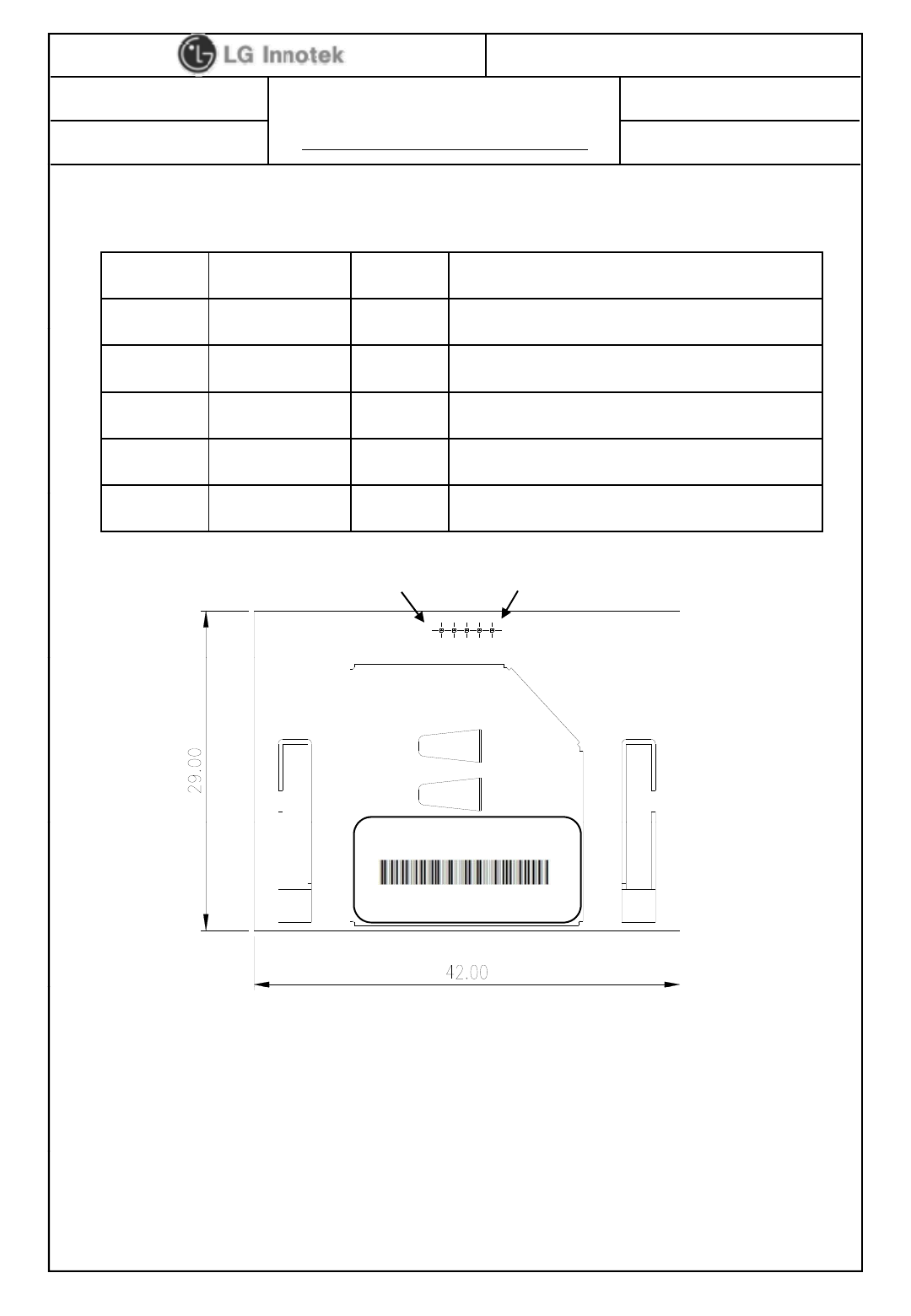
Size : 42mm x 29mm x 6mm
2.4GHz and 5GHz internal PA
Two stream spatial multiplexing up to 300Mbps
Monopole ANT (2T2R MIMO)
Use on-chip OTP (One-Time Programmable)
USB 2.0
Supports drivers for Windows Vista, 2000, XP, Linux
Security : WPA,WPA2,AES(TKIP) ,IEEE 802.1X
• Application: DTV, DVR, HD DVD Player, Blue-ray Disk Player, STB
2. Ordering Information
Model Description
TWFM-B001T Wi-Fi Module, Dual Band 2T2R MIMO
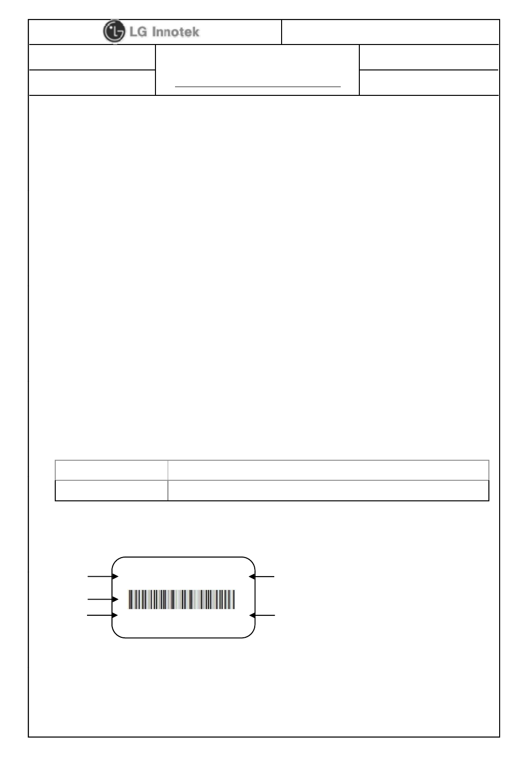
3. Label marking
①
④
①
②
③
①Model No ④Product Lot No. : 1009A2901
TWFM-B001T 1009A2901
001EB2B00339 15351616
④
⑤
©2010 LGIT. All rights reserved.
②MAC Address BAR Code -10 : Year - 29 : Date
③MAC Address No. - 09: Month - 01 : Manufactured
⑤PIN Code - Revision No. : A Process
S P E C I F I C A T I O N
PAGE :
DOCUMENT No :
REG. DATE : 2010.11.16
MODEL NAME : TWFM-B001T
REV. DATE : 2010.11.16
REV.NO : 1.0
HC40645
2/ 16
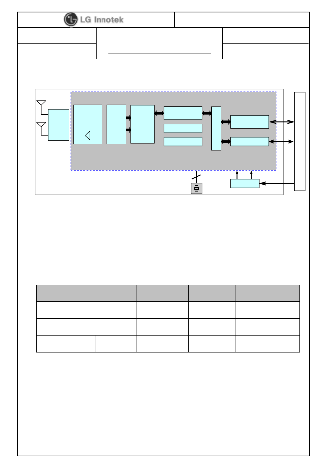
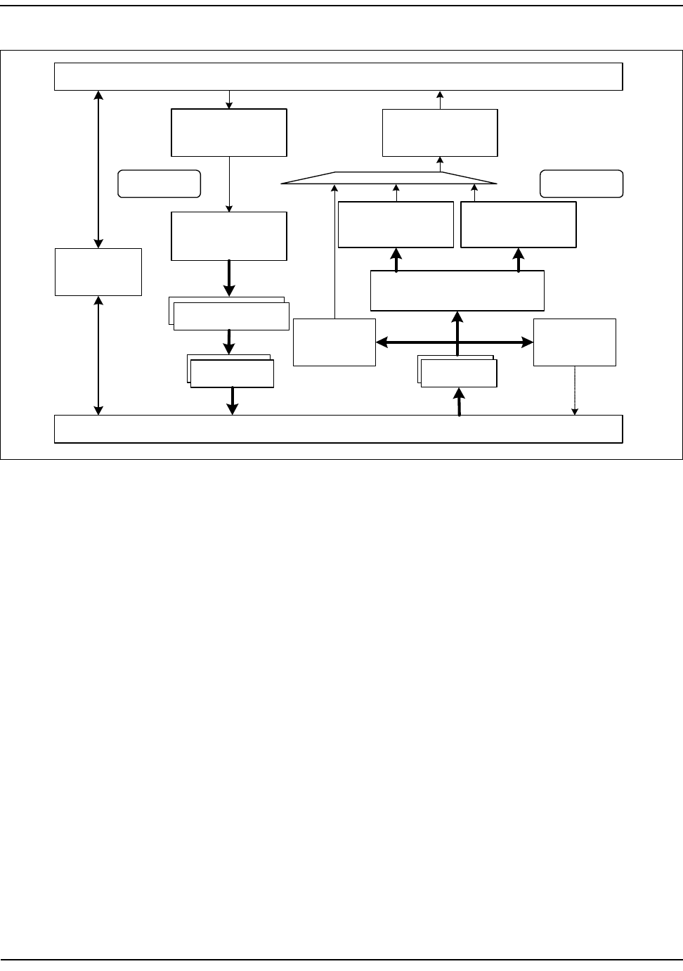
RF
802.11n MAC
ANT
I
n
USB 2 0
ANT
BCM43236
4. Block Diagram
RF
Switch+
diplexer
3.3V 1.2V
2.4GHz PA
5GHz PA
2 x 2
Radio
802.11n
PHY Security
OTP(2K bits)
n
ternal Bus
GPIO
USB
2
.
0
or
HSIC
ANT
USB Connector
5. Absolute Maximum Ratings
Main Clock(20MHz) DC-DC
5V
< Fig.1 Hardware Block Diagram >
Caution : The s
p
ecifications in Table 1 define levels at which
p
ermanent dama
g
e to the
Parameter
Min
Max
Unit
ppg
device can occur. Function operation is not guaranteed under these conditions.
Operating at absolute maximum conditions for extend periods can adversely affect the
long-term reliability of the device.
Parameter
Min
Max
Unit
Storage Temperature -10 +80 ℃
Storage Humidity - 90 %
Supply Voltage VDD_5V - 6.0 Vdc
< Table 1 Absolute Maximum Ratings >
. Other conditions
1) Do not use or store modules in the corrosive atmosphere, especially where chloride
gas, sulfide gas, acid, alkali, salt or the like are contained.
Also, avoid exposure to moisture.
2) Store the modules where the temperature
©2010 LGIT. All rights reserved.
2)
Store
the
modules
where
the
temperature
and relative humidity do not exceed 5 to 40℃and 20 to 60%.
3) Assemble the modules within 6 months.
Check the soldering ability in case of 6 months over.

S P E C I F I C A T I O N
PAGE :
DOCUMENT No :
REG. DATE : 2010.11.16
MODEL NAME : TWFM-B001T
REV. DATE : 2010.11.16
REV.NO : 1.0
HC40645
3/ 16
6. Operating Conditions
Parameter Min Typ Max Unit
Operating Temperature 0 - +60 ℃
Operating Humidity - - 85 %
Supply
Voltage VDD_5V 4.5 - 5.5 Vdc
7. Standard Test Conditions
Th T t f l t i l ifi ti h ll b f d d th f ll i diti
Th
e
T
es
t
f
or e
l
ec
t
r
i
ca
l
spec
ifi
ca
ti
on s
h
a
ll
b
e per
f
orme
d
un
d
er
th
e
f
o
ll
ow
i
ng con
diti
on
unless otherwise specified.
1). Ambient condition
. Temperature : 25℃±5℃
. Humidity : 65% ±5% R.H.
2) Power supply voltages
2)
.
Power
supply
voltages
. 5V (±5%) input power at the Module
3). Current consumption over recommended range of supply voltage and operating
conditions is like below.
When it’s tested, it must be supplied more than 2 times of maximal current.
FCC (Federal Communications Commission)
WARNING Thi i t t di f
WARNING
:
Thi
s equ
i
pmen
t
may genera
t
e or use ra
di
o
f
requency energy.
Changes or modifications to this equipment may cause harmful interference unless the modifications are expressly
approved in the instruction manual. The user could lose the authority to operate this equipment if an unauthorized
change or modification is made.
This device complies with Part 15 of the FCC`s Rules. Operation is subject to the following two Conditions:
1. This device may not cause harmful interference, and
2. This device must accept ant interference received, including interference that may cause undesirable operation.
To satisfy FCC exterior labeling requirements the following text must be placed on the exterior of the end product
To
satisfy
FCC
exterior
labeling
requirements
,
the
following
text
must
be
placed
on
the
exterior
of
the
end
product
.
Contains Transmitter module FCC ID: YZP-TWFMB001T
The antenna must be installed such that 20 cm is maintained between the antenna and users, and the transmitter
module may not be co-located with any other transmitter or antenna. End users cannot modify this transmitter
device. Any Unauthorized modification could void the user‘s authority to operate this device.
©2010 LGIT. All rights reserved.

S P E C I F I C A T I O N
PAGE :
DOCUMENT No :
REG. DATE : 2010.11.16
MODEL NAME : TWFM-B001T
REV. DATE : 2010.11.16
REV.NO : 1.0
HC40645
4/ 16
8. Electrical Specifications
Current Consumption Min. Typ. Max. Unit
TX Mode ( MCS7) - 470 -
mA
Idle and Associated state
-
210
-
1) DC Characteristics
Items Contents
2) RF Characteristics for IEEE802.11b ( 11Mbps mode unless otherwise specified)
mA
Idle
and
Associated
state
210
Radio disabled state - 60 -
Specification IEEE802.11b
Mode DSSS/CCK
Channel frequency 2400 ~ 2483 MHz
Data rate 1,2,5.5,11Mbps
TX Characteristics Min. Typ. Max. Unit
Power Level 13 15 17 dBm
Spectrum Mask
1st side lobes - -38 -30 dBr
2nd side lobes - -54 -50 dBr
Modulation Accuracy (EVM) - - 35 %
Power On/Off ramp - - 2.0 Usec
Spurious Emissions (BW=100kHz)
30-1000MHz - - -36 dBm
1000-12750MHz - - -30 dBm
RX Characteristics Min. Typ. Max. Unit
Minimum Input Level Sens. (FER ≤ 8%) -88 -78 dBm
©2010 LGIT. All rights reserved.
Maximum Input Level (FER ≤ 8%) -10 - - dBm
* Normal Condition : 25℃, VDD=5V.

S P E C I F I C A T I O N
PAGE :
DOCUMENT No :
REG. DATE : 2010.11.16
MODEL NAME : TWFM-B001T
REV. DATE : 2010.11.16
REV.NO : 1.0
HC40645
5/ 16
Items Contents
Specification
IEEE802.11g
3) RF Characteristics for IEEE802.11g ( 54Mbps mode unless otherwise specified)
Specification
IEEE802.11g
Mode OFDM
Channel frequency 2400 ~ 2483 MHz
Data rate 6,9,12,18,24,36,48,54Mbps
TX Characteristics Min. Typ. Max. Unit
Power Level 13 15 17 dBm
Spectrum Mask
tf /
11MH
32
21
dB
a
t
f
c +
/
-
11MH
z--
32
-
21
dBr
at fc +/-20MHz - -35 -29 dBr
at fc ≥ +/- 30MHz - -45 -41 dBr
Constellation Error (EVM) - -28 -25 dB
Spurious Emissions (BW=100kHz)
30-1000MHz - - -36 dBm
1000-12750MHz - - -30 dBm
RX Characteristics Min. Typ. Max. Unit
Minimum Input Level Sens. (PER ≤ 10%) - -73 -65 dBm
Maximum Input Level (PER ≤ 10%) -20 - - dBm
©2010 LGIT. All rights reserved.
* Normal Condition : 25℃, VDD=5V.

S P E C I F I C A T I O N
PAGE :
DOCUMENT No :
REG. DATE : 2010.11.16
MODEL NAME : TWFM-B001T
REV. DATE : 2010.11.16
REV.NO : 1.0
HC40645
6/ 16
Items Contents
4) RF Characteristics for IEEE802.11a ( 54Mbps mode unless otherwise specified)
Specification IEEE802.11a
Mode OFDM
Channel frequency 5150~5250MHz, 5725 ~ 5850 MHz
Data rate 6,9,12,18,24,36,48,54Mbps
TX Characteristics Min. Typ. Max. Unit
Power Level 11 13 15 dBm
Spectrum Mask
Spectrum
Mask
at fc +/-11MHz - -32 -21 dBr
at fc +/-20MHz - -35 -29 dBr
at fc ≥ +/- 30MHz - -45 -41 dBr
Constellation Error (EVM) - -28 -25 dB
Spurious Emissions (BW=100kHz)
30-1000MHz - - -36 dBm
1000-12750MHz - - -30 dBm
RX Characteristics Min. Typ. Max. Unit
Minimum Input Level Sens. (PER ≤ 10%) - -73 -65 dBm
Maximum Input Level (PER ≤10%)
-
20
-
-
dBm
©2010 LGIT. All rights reserved.
Maximum
Input
Level
(PER
≤
10%)
-
20
-
-
dBm
* Normal Condition : 25℃, VDD=5V.

S P E C I F I C A T I O N
PAGE :
DOCUMENT No :
REG. DATE : 2010.11.16
MODEL NAME : TWFM-B001T
REV. DATE : 2010.11.16
REV.NO : 1.0
HC40645
7/ 16
Items Contents
Specification IEEE802.11n – 5GHz
5) RF Characteristics for IEEE802.11an
( MCS7 mode unless otherwise specified)
Mode OFDM
Channel frequency 5150~5250MHz, 5725 ~ 5850 MHz
Data rate 6.5,13,19.5,26,39,52,58.5,65Mbps
TX Characteristics
Min
Typ
Max
Unit
TX
Characteristics
Min
.
Typ
.
Max
.
Unit
Power Level (HT20 / HT40 : MCS7) 11 13 15 dBm
Spectrum Mask
at fc +/-11MHz - -32 -21 dBr
at fc +/-20MHz - -35 -29 dBr
at fc ≥ +/- 30MHz - -45 -41 dBr
Constellation Error (EVM) - -29 -28 dB
Spurious Emissions (BW=100kHz)
30-1000MHz - - -36 dBm
1000-12750MHz - - -30 dBm
RX Characteristics Min. Typ. Max. Unit
Minimum Input Level Sens.
(HT20,PER ≤ 10%) --70-64dBm
Minimum Input Level Sens.
(HT40,PER ≤ 10%) --66-62dBm
(%)
©2010 LGIT. All rights reserved.
Maximum Input Level
(
PER ≤ 10
%)
-20 - - dBm
* Normal Condition : 25℃, VDD=5V.

S P E C I F I C A T I O N
PAGE :
DOCUMENT No :
REG. DATE : 2010.11.16
MODEL NAME : TWFM-B001T
REV. DATE : 2010.11.16
REV.NO : 1.0
HC40645
8/ 16
Items Contents
6) RF Characteristics for IEEE802.11gn
( MCS7 mode unless otherwise specified)
Specification IEEE802.11n – 2.4GHz
Mode OFDM
Channel frequency 2400 ~ 2483 MHz
Data rate 6.5
,
13
,
19.5
,
26
,
39
,
52
,
58.5
,
65Mb
p
s
,, ,,,, , p
TX Characteristics Min. Typ. Max. Unit
Power Level (HT20/HT40 : MCS7) 13 15 17 dBm
Spectrum Mask
at fc +/
11MHz
32
21
dBr
at
fc
+/
-
11MHz
--
32
-
21
dBr
at fc +/-20MHz - -35 -29 dBr
at fc ≥ +/- 30MHz - - -45 dBr
Constellation Error (EVM) - -29 -28 dB
S i E i i (BW 100kH )
S
pur
i
ous
E
m
i
ss
i
ons
(BW
=
100kH
z
)
30-1000MHz - - -36 dBm
1000-12750MHz - - -30 dBm
RX Characteristics Min. Typ. Max. Unit
Minimum Input Level Sens.
(HT20,PER ≤ 10%) --68-64dBm
Minimum Input Level Sens.
(HT40,PER ≤ 10%) --66-62dBm
M i I t L l (PER ≤10%)
20
dB
©2010 LGIT. All rights reserved.
M
ax
i
mum
I
npu
t
L
eve
l
(PER
≤
10%)
-
20
--
dB
m
* Normal Condition : 25℃, VDD=5V.

S P E C I F I C A T I O N
PAGE :
DOCUMENT No :
REG. DATE : 2010.11.16
MODEL NAME : TWFM-B001T
REV. DATE : 2010.11.16
REV.NO : 1.0
HC40645
9/ 16
9. Environment Tests
Item Test Conditions Specifications
Initial values are measured at standard test condition.
Heat Load
Test
Leave samples in 60℃±2℃for 96 ±5 hours, and in
standard test condition for 30 minutes, then take
measurements within 1 hour.
- Supply voltage : standard ±5%
- Supply voltage cycle : 1.5h on, 0.5h off
Humidity
Load Test
Initial values are measured at standard test condition.
Leave samples in 40℃±5℃, 90 ~ 95% RH for 96 ±5
hours, and in standard test condition for 30 minutes,
then take measurements within 1 hour.
- Supply voltage : standard + 5%
Supply voltage cycle : 1 5h on 0 5h off
•TX Power
: ±4dB Max
• Min Input
Level
±
4dB M
-
Supply
voltage
cycle
:
1
.
5h
on
,
0
.
5h
off
High
Temperature
Test
Initial values are measured at standard test condition.
Leave samples in 80℃±2℃for 96 ±5 hours, and
in standard ambient for 1 hour with standard power
Supply then take measurements within 1 hour.
:
±
4dB
M
ax
Cold Test
Initial values are measured at standard test condition.
Leave samples in -40℃±2℃for 96 ±5 hours, and
in standard ambient for 1 hour with standard power
Supply then take measurements within 1 hour
Supply
then
take
measurements
within
1
hour
.
Temperature
Shock
Take measurements in standard test condition.
Temp. : -40℃~ +85℃
Duration : 30 min
©2010 LGIT. All rights reserved.
Shock
Ramp-up & Ramp-down for 5 min
Cycle : 200cycle.
S P E C I F I C A T I O N
PAGE :
DOCUMENT No :
REG. DATE : 2010.11.16
MODEL NAME : TWFM-B001T
REV. DATE : 2010.11.16
REV.NO : 1.0
HC40645
10 / 16
10. Pin Description
Pin No. Pin Name I/O Pin Description
1W
a
k
e
-
up
O
Co
n
t
r
o
l
s
i
g
n
a
l f
o
r w
a
k
e
-
up
1
Wake
up
O
Control
signal
for
wake
up
2 GND - GND
3 USB_DP I/O USB Communication signal USB_DP
4 USB_DN I/O USB Communication signal USB_DN
5 VDD I VDD 5V
< TOP View > ①⑤
TWFM-B001T
001EB2B00339
1009A2901
15351616
Note.
. Recommend a Module install sequence for prevent USB device failure
1) Supply 5V power
2) Connect to data signal (USB_DP, USB_DN)
. If remove the module, proceed in reveres sequence
©2010 LGIT. All rights reserved.

S P E C I F I C A T I O N
PAGE :
DOCUMENT No :
REG. DATE : 2010.11.16
MODEL NAME : TWFM-B001T
REV. DATE : 2010.11.16
REV.NO : 1.0
HC40645
11 / 16
11. S/W
The module is controlled by wl command. It is intended for those evaluating
and/or testing Broadcom’s IC, describes a subset of the commands available in wl,
the Broadcom ® WLAN client utility.
1) Command Syntax
The syntax is as follows:
wl <adapter> [-h] [-d|u|x] <command> [arguments]
where
-h this message and command descriptions
-d output format signed integer
-u output format unsigned integer
-x output format hexdecimal
The [h,u] option is only to print help.
Other syntax specifics are as follows:
• Entries within square brackets, such as [arguments], are optional. In the above example,
switches within brackets, such as –h, are typed as shown. The |symbol should not be
typed,
it represents the word or.
• Entries within angle brackets, such as <adapter>, are required and indicate that a value
must
be inserted in place of the item contained within the angle brackets.
•
Entries shown outside of either square or angle brackets are to be typed as shown
Entries
shown
outside
of
either
square
or
angle
brackets
are
to
be
typed
as
shown
.
2) Command List and Version
•CMDS
Syntax: wl cmds
Pur
p
ose: Generates a list of available commands.
p
Parameters:None
Returns: All commands available to the attached 43XX chip.
•VER
Syntax: wl ver
Purpose: Generates a list of available commands.
Parameters:
None
©2010 LGIT. All rights reserved.
Parameters:
None
Returns: All commands available to the attached 43XX chip.
•Please refer to ‘80211-TI201-R’ technical document of Broadcom to other
commands.

12/20/2010 CTJ5M
CONFIDENTIAL FOR LG INNOTEK CO LTD
Preliminary Data Sheet
BCM43236
43236-DS04-R
5300 California Avenue • Irvine, CA 92617 • Phone: 949-926-5000 • Fax: 949-926-5203 December 17, 2010
2.4 GHz/5 GHz IEEE802.11n MAC/PHY/Radio Chip
GENERAL DESCRIPTION
FEATURES
The BCM43236 is a dual-band (2.4 GHz and 5 GHz)
IEEE 802.11n-compliant MAC/PHY/Radio complete
system-on-a-chip with 2.4 GHz and 5 GHz internal
PAs. The device enables the development of USB
2.0- or HSIC-based IEEE 802.11n WLAN client and
router subsystem solutions. The BCM43236 is
targeted for all WLAN markets that can take
advantage of the high throughput and extended
range of the Broadcom second-generation MIMO
solution. With MIMO, information is sent and
received over two or more antennas simultaneously
using the same frequency band thus providing
greater range and increasing throughput, while
maintaining compatibility with legacy IEEE 802.11a/
b/g devices. This is accomplished through a
combination of enhanced MAC and PHY
implementations including spatial multiplexing
modes in the transmitter and receiver and advanced
digital signal processing techniques to improve
receive sensitivity.
The BCM43236 architecture with its fully integrated
dual-band radio transceiver supports
2 × 2 antennas for Layer 2 throughput of over
200 Mbps.
State-of-the-art security is provided by industry
standardized system support for WPA™, WPA2™
(IEEE 802.11i), and hardware-accelerated AES
encryption/decryption, coupled with TKIP and IEEE
802.1X support. Embedded hardware acceleration
enables increased system performance and
significant reduction in host-CPU utilization in both
client and access point configurations. The
BCM43236 also supports Broadcom’s widely
accepted and deployed WPS for ease-of-use
wireless secured networks.
• IEEE 802.11n-compliant
• 2.4 GHz and 5 GHz internal PA
• Two-stream spatial multiplexing up to 300 Mbps
• Uses on-chip OTP (One-Time Programmable)
memory instead of SROM for substantial RBOM
savings.
• Supports MCS 0–15 and MCS 32 modulation and
coding rates.
• Supports 20 MHz and 40 MHz channels with optional
SGI.
• Support for STBC in both TX and RX
• Greenfield, mixed mode, and legacy modes
supported
• Full IEEE 802.11a/b/g legacy compatibility with
enhanced performance.
• Supports one USB 2.0 host port or one 480 MHz HSIC
port.
• UART and JTAG interface, up to eight GPIOs.
• Supports up to 32 MB of serial Flash™ memory.
• ARM® Cortex-M3™ CPU core plus 256 KB ROM and
448 KB RAM.
• Supports Broadcom’s OneDriver™ software.
• Supports WHQL certified drivers for Windows® Vista
32- and 64-bit, Windows® XP, and Windows 2000
operating systems for client applications.
• Supports Linux® and VxWorks® for access point and
router applications.
• Comprehensive wireless network security support
that includes WPA, WPA2, and AES encryption/
decryption coupled with TKIP and IEEE 802.1X
support.
• BCM43236 package: 10 mm x 10 mm 88-pin QFN
APPLICATIONS
• USB 2.0 dongles
• HSIC media modules
12/20/2010 CTJ5M
CONFIDENTIAL FOR LG INNOTEK CO LTD
Revision History
BROADCOM 2.4 GHz/5 GHz 802.11n MAC/PHY/Radio Chip
December 17, 2010 • 43236-DS04-R Page 2
®
BCM43236 Preliminary Data Sheet
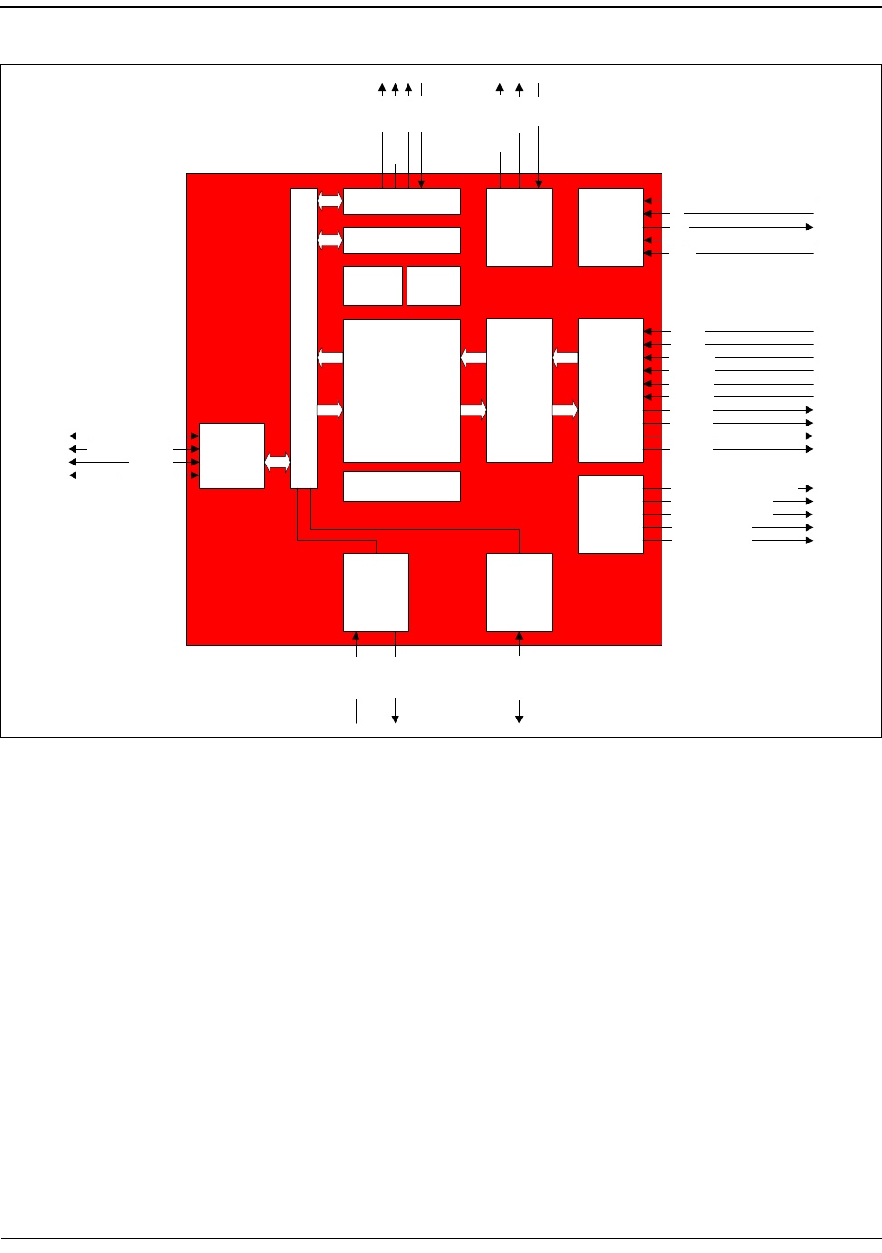
Figure 1: BCM43236 Block Diagram
802.11n MAC IEEE
802.11n
PHY
USB 2.0 Device
or HSIC
OTP (2 Kbits)
JTAG
GPIO
LED
Security
RF
Front
End
Internal Bus
(Switches)
2 × 2
Radio
2.4-Ghz PA
5-Ghz PA
BCM43236
Serial Flash
Interface
Flash Memory

12/20/2010 CTJ5M
CONFIDENTIAL FOR LG INNOTEK CO LTD
Revision History
BROADCOM 2.4 GHz/5 GHz 802.11n MAC/PHY/Radio Chip
December 17, 2010 • 43236-DS04-R Page 3
®
BCM43236 Preliminary Data Sheet
Revision History
Revision Date Change Description
43236-DS04-R 12/17/10 Updated:
•Table 7: “Current Consumption from 3.3V Supply,” on page 28
•Table 8: “Current Consumption from 1.2V Supply,” on page 28
•Figure 11: “BCM43236 Mechanical Drawing,” on page 39
43236-DS03-R 07/19/10 Updated:
• Section 3: “Pin Assignments,” on page 20.
• Table 3: “Signal Descriptions,” on page 22.
• Table 5: “Absolute Maximum Ratings,” on page 27.
• Section 8: “Thermal Information,” on page 38.
• Section 10: “Ordering Information,” on page 40.
Added:
• “HSIC Characteristics” on page 29.
43236-DS02-R 07/05/10 Updated:
• Figure 8: “BCM43236 88-Pin QFN Package,” on page 19.
• Table 2: “Pin Assignments,” on page 20.
• Table 3: “Signal Descriptions,” on page 21.
43236-DS01-R 04/30/10 Updated:
• Table 2: “Pin Assignments,” on page 19.
• Figure 7: “BCM43236 88-Pin QFN Package,” on page 18.
• Table 3: “Signal Descriptions,” on page 20.
• Table 4: “Strapping Options,” on page 24.
• Table 5: “Absolute Maximum Ratings,” on page 25.
• Table 6: “Recommended Operating Conditions and DC Characteristics,”
on page 26.
• Table 10: “2.4 GHz Band Receiver RF Specifications,” on page 27.
• Table 11: “2.4 GHz Band Transmitter RF Specifications,” on page 29.
• Table 13: “5 GHz Band Receiver RF Specifications,” on page 30.
• Table 14: “5 GHz Band Transmitter RF Specifications,” on page 31.
• Table 19: “88-Pin QFN Thermal Characteristics,” on page 35.
• Table 20: “Ordering Information,” on page 37.
Added:
• Table 7: “Current Consumption from 3.3V Supply,” on page 26.
• Table 8: “Current Consumption from 1.2V Supply,” on page 26.
43236-DS00-R 10/20/09 Initial release
12/20/2010 CTJ5M
CONFIDENTIAL FOR LG INNOTEK CO LTD
Broadcom®, the pulse logo, Connecting everything®, and the Connecting everything logo are among the
trademarks of Broadcom Corporation and/or its affiliates in the United States, certain other countries and/
or the EU. Any other trademarks or trade names mentioned are the property of their respective owners.
Any recommendations or changes to this document can be submitted to MCBUMktg@broadcom.com.
This data sheet (including, without limitation, the Broadcom component(s) identified herein) is not designed,
intended, or certified for use in any military, nuclear, medical, mass transportation, aviation, navigations,
pollution control, hazardous substances management, or other high risk application. BROADCOM PROVIDES
THIS DATA SHEET "AS-IS", WITHOUT WARRANTY OF ANY KIND. BROADCOM DISCLAIMS ALL WARRANTIES,
EXPRESSED AND IMPLIED, INCLUDING, WITHOUT LIMITATION, THE IMPLIED WARRANTIES OF
MERCHANTABILITY, FITNESS FOR A PARTICULAR PURPOSE, AND NON-INFRINGEMENT.
Broadcom Corporation
5300 California Avenue
Irvine, CA 92617
© 2010 by Broadcom Corporation
All rights reserved
Printed in the U.S.A.

12/20/2010 CTJ5M
CONFIDENTIAL FOR LG INNOTEK CO LTD
Table of Contents BCM43236 Preliminary Data Sheet
BROADCOM 2.4 GHz/5 GHz 802.11n MAC/PHY/Radio Chip
December 17, 2010 • 43236-DS04-R Page 5
®
Table of Contents
Section 1: Introduction...................................................................................................... 9
Section 2: Functional Description .................................................................................... 11
Global Functions...........................................................................................................................................11
Power Management ..............................................................................................................................11
Voltage Regulators.................................................................................................................................11
Reset ......................................................................................................................................................11
GPIO Interface........................................................................................................................................11
Bluetooth Coexistence Interface ...........................................................................................................12
OTP.........................................................................................................................................................12
JTAG Interface........................................................................................................................................12
UART Interface.......................................................................................................................................12
Serial Flash™ Interface...........................................................................................................................12
USB/HSIC Interface ................................................................................................................................13
Crystal Oscillator ....................................................................................................................................14
IEEE 802.11n MAC Description.....................................................................................................................15
IEEE 802.11n PHY Description ......................................................................................................................17
Dual-Band Radio Transceiver.......................................................................................................................19
Receiver Path .........................................................................................................................................19
Transmitter Path ....................................................................................................................................19
Calibration..............................................................................................................................................19
Section 3: Pin Assignments.............................................................................................. 20
BCM43236 88-Pin QFN Assignments ...........................................................................................................20
Signals by Pin Number ...........................................................................................................................21
Section 4: Signal and Pin Descriptions ............................................................................. 22
Package Signal Descriptions.........................................................................................................................22
Strapping Options.........................................................................................................................................26
Section 5: Electrical Characteristics.................................................................................. 27
Absolute Maximum Ratings.........................................................................................................................27
Recommended Operating Conditions and DC Characteristics....................................................................28
Current Consumption from the 3.3V Supply ...............................................................................................28
Current Consumption from the 1.2V Supply ...............................................................................................28

12/20/2010 CTJ5M
CONFIDENTIAL FOR LG INNOTEK CO LTD
Table of Contents
BROADCOM 2.4 GHz/5 GHz 802.11n MAC/PHY/Radio Chip
December 17, 2010 • 43236-DS04-R Page 6
®
BCM43236 Preliminary Data Sheet
HSIC Characteristics......................................................................................................................................29
Section 6: RF Specifications ............................................................................................. 30
2.4 GHz Band General RF Specifications ......................................................................................................30
2.4 GHz Band Receiver RF Specifications.....................................................................................................31
2.4 GHz Band Transmitter RF Specifications................................................................................................32
2.4 GHz Band Local Oscillator Specifications...............................................................................................32
5 GHz Band Receiver RF Specifications ........................................................................................................33
5 GHz Band Transmitter RF Specifications...................................................................................................34
5 GHz Band Local Oscillator Frequency Generator Specifications ..............................................................34
On-Chip Regulator Power Supply Characteristics .......................................................................................35
Section 7: Timing Characteristics ..................................................................................... 36
Reset and Clock Timing Diagram..................................................................................................................36
Serial Flash Timing Diagram .........................................................................................................................37
Section 8: Thermal Information....................................................................................... 38
Junction Temperature Estimation and PSIJT Versus ThetaJC .......................................................................38
Section 9: Package Information ....................................................................................... 39
Section 10: Ordering Information .................................................................................... 40

12/20/2010 CTJ5M
CONFIDENTIAL FOR LG INNOTEK CO LTD
List of Figures BCM43236 Preliminary Data Sheet
BROADCOM 2.4 GHz/5 GHz 802.11n MAC/PHY/Radio Chip
December 17, 2010 • 43236-DS04-R Page 7
®
List of Figures
Figure 1: BCM43236 Block Diagram ...................................................................................................................2
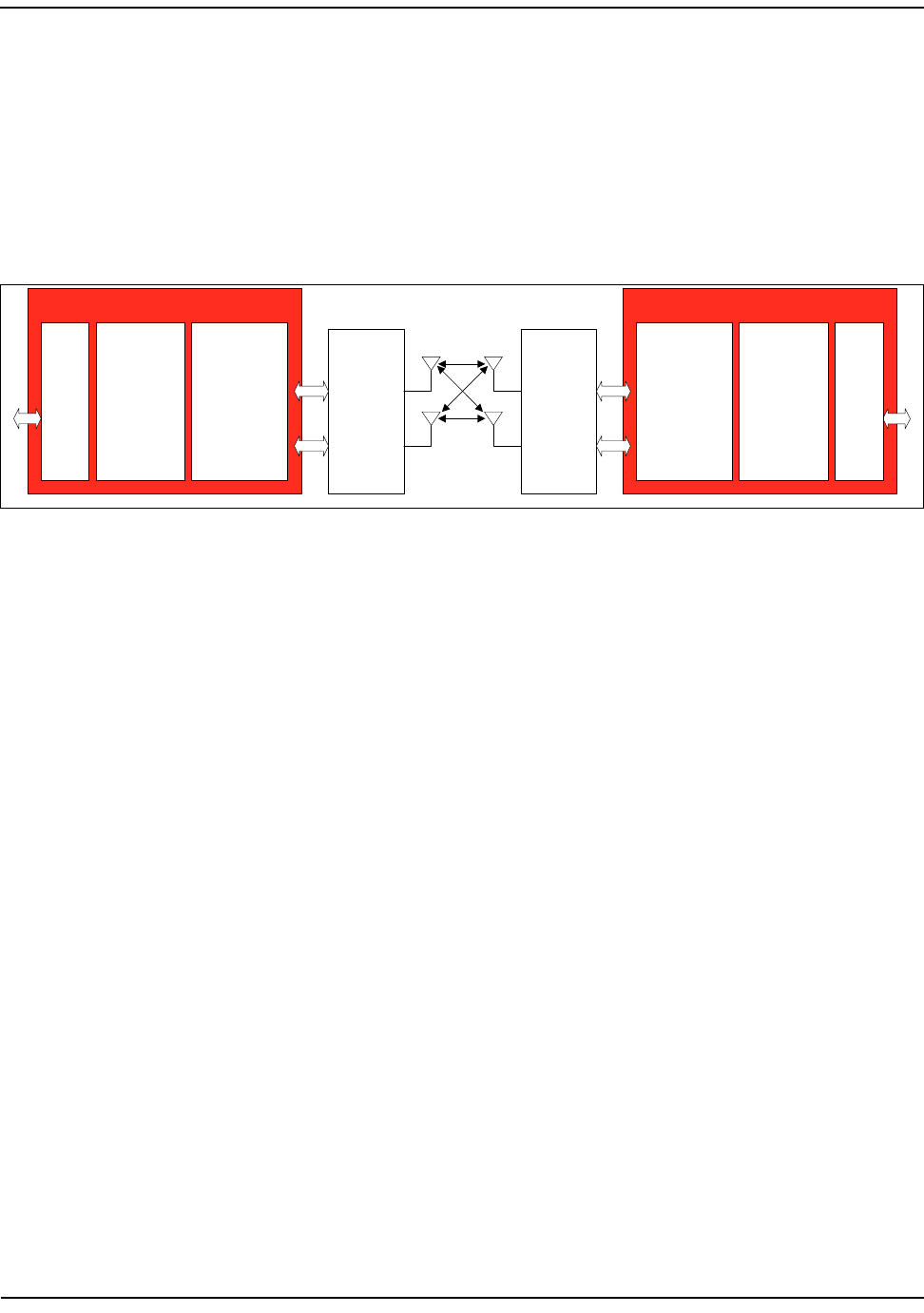
Figure 2: MIMO System Diagram Showing 2 × 2 Antenna Configuration ..........................................................9
Figure 3: Functional Block Diagram..................................................................................................................10
Figure 4: USB 2.0 Device/HSIC Core Block Diagram .........................................................................................13
Figure 5: Recommended Oscillator Configuration ...........................................................................................15
Figure 6: Enhanced MAC Block Diagram ..........................................................................................................16
Figure 7: PHY Block Diagram ............................................................................................................................18
Figure 8: BCM43236 88-Pin QFN Package........................................................................................................20
Figure 9: Timing for the Optional External Power-On Reset............................................................................36
Figure 10: Serial Flash Timing Diagram (STMicroelectronics-Compatible).......................................................37
Figure 11: BCM43236 Mechanical Drawing .....................................................................................................39

12/20/2010 CTJ5M
CONFIDENTIAL FOR LG INNOTEK CO LTD
List of Tables BCM43236 Preliminary Data Sheet
BROADCOM 2.4 GHz/5 GHz 802.11n MAC/PHY/Radio Chip
December 17, 2010 • 43236-DS04-R Page 8
®
List of Tables
Table 1: Crystal Oscillator Requirements .........................................................................................................14
Table 2: Pin Assignments..................................................................................................................................21
Table 3: Signal Descriptions..............................................................................................................................22
Table 4: Strapping Options...............................................................................................................................26
Table 5: Absolute Maximum Ratings................................................................................................................27
Table 6: Recommended Operating Conditions and DC Characteristics ...........................................................28
Table 7: Current Consumption from 3.3V Supply.............................................................................................28
Table 8: Current Consumption from 1.2V Supply.............................................................................................28
Table 9: HSIC Characteristics............................................................................................................................29
Table 10: 2.4 GHz Band General RF Specifications...........................................................................................30
Table 11: 2.4 GHz Band Receiver RF Specifications..........................................................................................31
Table 12: 2.4 GHz Band Transmitter RF Specifications.....................................................................................32
Table 13: 2.4 GHz Band Local Oscillator Specifications ....................................................................................32
Table 14: 5 GHz Band Receiver RF Specifications.............................................................................................33
Table 15: 5 GHz Band Transmitter RF Specifications........................................................................................34
Table 16: 5 GHz Band Local Oscillator Frequency Generator Specifications....................................................34
Table 17: On-Chip Regulator Power Supply Characteristics.............................................................................35
Table 18: Ext_por and Clock Timing .................................................................................................................36
Table 19: Serial Flash Timing ............................................................................................................................37
Table 20: 88-Pin QFN Thermal Characteristics.................................................................................................38
Table 21: Ordering Information .......................................................................................................................40
12/20/2010 CTJ5M
CONFIDENTIAL FOR LG INNOTEK CO LTD
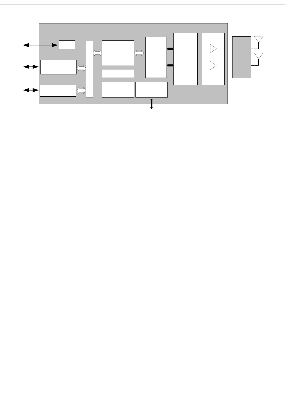
Introduction
BROADCOM 2.4 GHz/5 GHz 802.11n MAC/PHY/Radio Chip
December 17, 2010 • 43236-DS04-R Page 9
®
BCM43236 Preliminary Data Sheet
Section 1: Introduction
The BCM43236 is the latest innovative chip from Broadcom® based on IEEE 802.11n. The chip is designed to
take current WLAN systems to the next level of higher performance and greater range with Multiple Input
Multiple Output (MIMO) technology as shown in Figure 2. The IEEE 802.11n standard more than doubles the
spectral efficiency compared to that of current IEEE 802.11a/g WLANs.
Figure 2: MIMO System Diagram Showing 2 × 2 Antenna Configuration
Employing a native 32-bit bus with Direct Memory Access (DMA) architecture, the BCM43236 offers significant
performance improvements in transfer rates, CPU utilization, and flexible support for USB 2.0 devices.
Figure 3 on page 10 shows a block diagram of the device.
BCM43236
BCM43236
IEEE
802.11n
MAC/PHY
IEEE 802.11n
2.4-/5-GHz
Radio
Transceiver
with
Integrated
PAs
RF
Switches
Host
I/F RF
Switches
IEEE
802.11n
MAC/PHY
IEEE 802.11n
2.4-/5-GHz
Radio
Transceiver
with
Integrated
PAs
Host
I/F
12/20/2010 CTJ5M
CONFIDENTIAL FOR LG INNOTEK CO LTD
Introduction
BROADCOM 2.4 GHz/5 GHz 802.11n MAC/PHY/Radio Chip
December 17, 2010 • 43236-DS04-R Page 10
®
BCM43236 Preliminary Data Sheet
Figure 3: Functional Block Diagram
BCM43236
Internal Bus System
IEEE
802.11n
PHY
2.4/5 GHz
Radio
Security
RF
Control
UART
JTAG
Interface
UART_RX
UART_TX
GPIO
PLL
20 MHz
Ref.
Clock
SFLASH Interface
ROM
(256 KB)
ARMCortexM3
RAM
(448 KB)
USB 2.0
Device
or HSIC
IEEE 802.11n
MAC
GPIO[0:7]
antenna switch controls (10)
ext_lna_2g controls (4)
ext_lna_5g controls (4)
pa_2g controls (2)
pa_5g controls (2)
USB20_DEV_DPLS
USB20_DEV_DMNS
HSIC Data
HSIC Strobe
TRST#
TMS
TDI
TCLK
TDO
tssiln_0
tssiln_1
lna_p_a_0
lna_p_a_1
lna_p_g_0
lna_p_g_0
pa_p_a_0
pa_p_a_1
pa_p_g_0
pa_p_g_1
xtal_buf_out
xtal_out
xtal_in
sflash_d
extif_flash_cs_l
sflash_c
sflash_q

12/20/2010 CTJ5M
CONFIDENTIAL FOR LG INNOTEK CO LTD
Functional Description
BROADCOM 2.4 GHz/5 GHz 802.11n MAC/PHY/Radio Chip
December 17, 2010 • 43236-DS04-R Page 11
®
BCM43236 Preliminary Data Sheet
Section 2: Functional Description
Global Functions
Power Management
The BCM43236 has been designed with the stringent power consumption requirements of battery-powered
hosts in mind. All areas of the chip design were scrutinized to help reduce power consumption. Silicon
processes and cell libraries were chosen to reduce leakage current and supply voltages.
Additionally, the BCM43236 includes an advanced Power Management Unit (PMU). The PMU provides
significant power savings by putting the BCM43236 into various power management states appropriate to the
current environment and activities that are being performed. The power management unit enables and
disables internal regulators, switches, and other blocks based on a computation of the required resources and
a table that describes the relationship between resources and the time needed to enable and disable them.
Power-up sequences are fully programmable. Configurable, free-running counters in the PMU are used to turn
on/off individual regulators and power switches. Clock speeds are dynamically changed (or gated altogether)
for the current mode. Slower clock speeds are used wherever possible.
Voltage Regulators
Three Low-Dropout (LDO) regulators and a PMU are integrated into the BCM43236. All regulators are
programmable via the PMU.
Reset
Resets are generated internally by the BCM43236. An optional external power-on reset circuit can be
connected to the active-low Ext_por input pin. A 50 ms low pulse is recommended to guarantee that a
sufficiently long reset is applied to all internal circuits, including integrated PHYs. The initialization process loads
all pin-configurable modes, resets all internal processes, and puts the device in the idle state. During
initialization, the clock source input signal must be active, and the 3.3V power supply to the device must be
stable. The external power-on reset overrides the BCM43236 internal reset.
GPIO Interface
There are eight General-Purpose I/O (GPIO) pins provided on the BCM43236. They are multiplexed with the
control signals. These pins can be used to attach to various external devices. Upon power-up and reset, these
pins become tristated. Subsequently, they can be programmed to be either input or output pins via the GPIO
control register. A programmable internal pull-up/pull-down resistor is included on each GPIO. If a GPIO output
enable is not asserted, and the corresponding GPIO signal is not being driven externally, the GPIO state is
determined by its programmable resistor.

12/20/2010 CTJ5M
CONFIDENTIAL FOR LG INNOTEK CO LTD
Global Functions
BROADCOM 2.4 GHz/5 GHz 802.11n MAC/PHY/Radio Chip
December 17, 2010 • 43236-DS04-R Page 12
®
BCM43236 Preliminary Data Sheet
Bluetooth Coexistence Interface
A 5-wire handshake interface is provided to enable signalling between the device and an external Bluetooth
device host to manage sharing of the wireless medium for optimum performance. The signals provided are:
•btcx_tx_conf
• btcx_rf_active
• btcx_status
•btcx_prisel
•btcx_freq
OTP
The BCM43236 contains an on-chip One-Time-Programmable (OTP) area that can be used for nonvolatile
storage of WLAN information such as a MAC address and other hardware-specific parameters. The total area
available for programming is 2 Kbits.
JTAG Interface
The BCM43236 supports the IEEE 1149.1 JTAG boundary-scan standard for testing the device packaging and
PCB manufacturing.
UART Interface
One UART interface is provided that can be attached to RS-232 Data Termination Equipment (DTE) for
exchanging and managing data with other serial devices. The UART interface is primarily used for debugging
and development.
Serial Flash™ Interface
Serial Flash™ is available regardless of whether USB 2.0 operation is enabled or disabled. The Flash interface is
an STMicroelectronics®-compatible 4-pin interface.
Note: These five pins are muxed with the JTAG interface.
12/20/2010 CTJ5M
CONFIDENTIAL FOR LG INNOTEK CO LTD
Global Functions
BROADCOM 2.4 GHz/5 GHz 802.11n MAC/PHY/Radio Chip
December 17, 2010 • 43236-DS04-R Page 13
®
BCM43236 Preliminary Data Sheet
USB/HSIC Interface
The BCM43236 USB/HSIC interface can be set to operate as a USB 2.0 port or a High-Speed Inter-Chip (HSIC)
port. Features of the interface are:
• USB 2.0 protocol engine:
– Parallel Interface Engine (PIE) between packet buffers and USB transceiver
– Supports up to nine endpoints, including Configurable Control Endpoint 0
• Separate endpoint packet buffers with a 512-byte FIFO buffer each
• Host-to-device communication for bulk, control, and interrupt transfers
• Configuration/status registers
• The HSIC port can communicate with an external HSIC host, such as the BCM5357 and BCM5358.
The various blocks in the USB 2.0 device/HSIC core are shown in Figure 4.
Figure 4: USB 2.0 Device/HSIC Core Block Diagram
The USB 2.0 PHY handles the USB protocol and the serial signaling interface between the host and device. It is
primarily responsible for data transmission and recovery. On the transmit side, data is encoded, along with a
clock, using the NRZI scheme with bit stuffing to ensure that the receiver detects a transition in the data
stream. A SYNC field that precedes each packet enables the receiver to synchronize the data and clock recovery
circuits. On the receive side, the serial data is deserialized, unstuffed, and checked for errors. The recovered
data and clock are then shifted to the clock domain that is compatible with the internal bus logic.
USB 2.0 Device
or HSIC
TX
FIFO
TX
FIFO
TX
FIFO
TX
FIFO
TX
FIFOs
DMA Engines
RX
FIFO
Endpoint Management Unit
USB 2.0
Protocol Engine
HSIC PHY USB 2.0 PHY
Data Strobe D+ D-
32-bit On-Chip Communication System

12/20/2010 CTJ5M
CONFIDENTIAL FOR LG INNOTEK CO LTD
Global Functions
BROADCOM 2.4 GHz/5 GHz 802.11n MAC/PHY/Radio Chip
December 17, 2010 • 43236-DS04-R Page 14
®
BCM43236 Preliminary Data Sheet
The endpoint management unit contains the PIE control logic and the endpoint logic. The PIE interfaces
between the packet buffers and the USB transceiver. It handles packet identification (PID), USB packets, and
transactions.
The endpoint logic contains nine uniquely-addressable endpoints. These endpoints are the source or sink of
communication flow between the host and the device. Endpoint zero is used as a default control port for both
the input and output directions. The USB system software uses this default control method to initialize and
configure the device information, and allows USB status and control access. Endpoint zero is always accessible
after a device is attached, powered, and reset.
Endpoints are supported by 512-byte FIFO buffers, one for each IN endpoint and one shared by all OUT
endpoints. Both TX and RX data transfers support a DMA burst of 4, which guarantees low latency and
maximum throughput performance. The RX FIFO can never overflow by design. The maximum USB packet size
cannot be more than 512 bytes.
Finally, the BCM43236 is either configured as a USB 2.0 device or as a PHY-less HSIC by selecting the
appropriate strapping option. See Table 4 on page 26 for information on how to select the strapping options.
Crystal Oscillator
Table 1 lists the requirements for the crystal oscillator.
Table 1: Crystal Oscillator Requirements
Parameter Value
Frequency 20 MHz
Mode AT cut, fundamental
Load capacitance 16 pF
ESR 50Ω maximum
Frequency stability ±10 ppm at 25°C
±10 ppm at 0°C to +85°C
Aging ±3 ppm/year max first year, ±1 ppm thereafter
Drive level 300 µW maximum
Q-factor 40,000 minimum
Shunt capacitance < 5 pF

12/20/2010 CTJ5M
CONFIDENTIAL FOR LG INNOTEK CO LTD
IEEE 802.11n MAC Description
BROADCOM 2.4 GHz/5 GHz 802.11n MAC/PHY/Radio Chip
December 17, 2010 • 43236-DS04-R Page 15
®
BCM43236 Preliminary Data Sheet
Figure 5 shows the recommended oscillator configuration.
Figure 5: Recommended Oscillator Configuration
IEEE 802.11n MAC Description
The IEEE 802.11n MAC features include:
• Enhanced MAC for supporting IEEE 802.11n features
• Programmable Access Point (AP) or Station (STA) functionality
• Programmable Independent Basic Service Set (IBSS) or infrastructure mode
• Aggregated MPDU (MAC Protocol Data Unit) support for High-throughput (HT)
• Passive scanning
• Network Allocation Vector (NAV), Interframe Space (IFS), and Timing Synchronization Function (TSF)
functionality
• RTS/CTS procedure
• Transmission of response frames (ACK/CTS)
• Address filtering of receive frames as specified by IBSS rules
• Multirate support
• Programmable Target Beacon Transmission Time (TBTT), beacon transmission/cancellation and
programmable Announcement Traffic Indication Message (ATIM) window
• CF conformance: Setting NAV for neighborhood Point Coordination Function (PCF) operation
• Security through a variety of encryption schemes including WEP, TKIP, AES, WPA™, WAP2™, and
IEEE 802.1X
• Power management
• Statistics counters for MIB support
The MAC core supports the transmission and reception of sequences of packets, together with related timing,
without any packet-by-packet driver interaction. Time-critical tasks requiring response times of only a few
milliseconds are handled in the MAC core. This achieves the required timing on the medium while keeping the
host driver easier to write and maintain. Also, incoming packets are buffered in the MAC core, which allows the
MAC driver to process them in bursts, enabling high bandwidth performance.
1M
27 pF
27 pF
221
OCS IN
OCS OUT
NOTE: See Reference Schematics
12/20/2010 CTJ5M
CONFIDENTIAL FOR LG INNOTEK CO LTD
IEEE 802.11n MAC Description
BROADCOM 2.4 GHz/5 GHz 802.11n MAC/PHY/Radio Chip
December 17, 2010 • 43236-DS04-R Page 16
®
BCM43236 Preliminary Data Sheet
The MAC driver interacts with the MAC core to prepare queues of packets to transmit and to analyze and
forward received packets to upper software layers. The internal blocks of the MAC core are connected to a
Programmable State Machine (PSM) through the host interface that connects to the internal bus (see
Figure 6).
Figure 6: Enhanced MAC Block Diagram
The host interface consists of registers for controlling and monitoring the status of the MAC core and
interfacing with the TX/RX FIFOs. For transmit, a total of 128 KB FIFO buffering is available that can be
dynamically allocated to six transmit queues plus template space for beacons, ACKs, and probe responses.
Whenever the host has a frame to transmit, the host queues the frame into one of the transmit FIFOs with a
TX descriptor containing TX control information. The PSM schedules the transmission on the medium
depending on the frame type, transmission rules in IEEE 802.11 protocol, and the current medium occupancy
scenario. After the transmission is completed, a TX status is returned to the host, informing the host of the
result that got transmitted.
The MAC contains a single 10 KB RX FIFO. When a frame is received, it is sent to the host along with an RX
descriptor that contains additional information about the frame reception conditions.
The power management block maintains the information regarding the power management state of the core
(and the associated STAs in case of an AP) to help in dynamic decisions by the core regarding frame
transmission.
The wireless security engine performs the required encryption/decryption on the TX/RX frames. This block
supports separate transmit and receive keys with four shared keys and 50 link-specific keys. The link-specific
keys are used to establish a secure link between any two STAs, with the required key being shared between
only those two STAs, hence excluding all of the other STAs in the same network from deciphering the
communication between those two STAs. The wireless security engine supports the following encryption
schemes that can be selected on a per-destination basis:
• None: The wireless security engine acts as a pass-through
• WEP: 40-bit secure key and 24-bit IV as defined in IEEE Std. 802.11-2007
• WEP128: 104-bit secure key and 24-bit IV
• TKIP: IEEE Std. 802.11-2007
• AES: IEEE Std. 802.11-2007
Host Interface
(Host Registers)
TX Status FIFO Six TX FIFOs
Template RX FIFO Code Memory
PHY Interface
Data Memory
Power
Management Wireless Security Engine Programmable
State Machine
(PSM)
Timing and
Control
TX Engine RX Engine

12/20/2010 CTJ5M
CONFIDENTIAL FOR LG INNOTEK CO LTD
IEEE 802.11n PHY Description
BROADCOM 2.4 GHz/5 GHz 802.11n MAC/PHY/Radio Chip
December 17, 2010 • 43236-DS04-R Page 17
®
BCM43236 Preliminary Data Sheet
The transmit engine is responsible for the byte flow from the TX FIFO to the PHY interface through the
encryption engine and the addition of an FCS (CRC-32) as required by IEEE 802.11-2007. Similarly, the receive
engine is responsible for byte flow from the PHY interface to the RX FIFO through the decryption engine and
for detection of errors in the RX frame.
The timing block performs the TSF, NAV, and IFS functionality as described in IEEE Std. 802.11-2007.
The Programmable State Machine (PSM) coordinates the operation of different hardware blocks required for
both transmission and reception. The PSM also maintains the statistics counters required for MIB support.
IEEE 802.11n PHY Description
The PHY features include:
• Programmable data rates from MCS 0–15 in 20 MHz and 40 MHz channels, as specified in IEEE 802.11n.
• Support for Short Guard Interval (SGI) and Space-Time Block Coding (STBC)
• All scrambling, encoding, forward error correction, and modulation in the transmit direction, and inverse
operations in the receive direction
• Advanced digital signal processing technology for best-in-class receive sensitivity
• Both mixed-mode and optional greenfield preamble of IEEE 802.11n
• Both long and optional short preambles of IEEE 802.11b
• Resistance to multipath (>250 nanoseconds RMS delay spread) with maximal ratio combining for high
throughput and range performance, including improved performance in legacy mode over existing IEEE
802.11a/b/g solutions.
• Automatic Gain Control (AGC)
• Available per-packet channel quality and signal strength measurements
The dual PHYs integrated in the BCM43236 provide baseband processing at all mandatory data rates specified
in IEEE 802.11n up to 300 Mbps, and the legacy rates specified in IEEE 802.11a/b/g including 1, 2, 5.5, 6, 9, 11,
12, 18, 24, 36, 48, and 54 Mbps. This core acts as an intermediary between the MAC and the dual-band
2.4/5 GHz radio, converting back and forth between packets and baseband waveforms.
12/20/2010 CTJ5M
CONFIDENTIAL FOR LG INNOTEK CO LTD
IEEE 802.11n PHY Description
BROADCOM 2.4 GHz/5 GHz 802.11n MAC/PHY/Radio Chip
December 17, 2010 • 43236-DS04-R Page 18
®
BCM43236 Preliminary Data Sheet
Figure 7: PHY Block Diagram
Descramble and
Deframe
Timing and Frequency Correction
TX FSM RX FSM
MAC Interface
ADC
ADC
Rake Receiver and
DPSK Demodulation
Equalizer and CCK
Demodulation
DAC DAC
TX Filter
TX Filter
Modulate/Spread
Frame and Scramble
PHY-to-Radio Interface
Sync/AGC
PHY Registers
MIMO
OFDM

12/20/2010 CTJ5M
CONFIDENTIAL FOR LG INNOTEK CO LTD
Dual-Band Radio Transceiver
BROADCOM 2.4 GHz/5 GHz 802.11n MAC/PHY/Radio Chip
December 17, 2010 • 43236-DS04-R Page 19
®
BCM43236 Preliminary Data Sheet
Dual-Band Radio Transceiver
Integrated into the BCM43236 is Broadcom's world-class dual-band radio transceiver that ensures low power
consumption and robust communications for low-cost applications operating in the 2.4 GHz and 5 GHz bands.
Channel bandwidths of 20 MHz and 40 MHz are supported as specified in IEEE 802.11n.
Receiver Path
The BCM43236 has a wide dynamic range, direct conversion receiver. It employs high order on-chip channel
filtering to ensure reliable operation in the noisy 2.4 GHz ISM band or the entire 5 GHz U-NII band. The
excellent noise figure of the receiver makes an external LNA unnecessary.
Transmitter Path
Baseband data is modulated and upconverted to the 2.4 GHz ISM band or the 5 GHz U-NII bands, respectively.
Linear on-chip Power Amplifiers are included, which are capable of delivering a nominal output power
exceeding +15 dBm while meeting the IEEE 802.11a and 802.11g specifications. The TX gain has a 78 dB range
with a resolution of 0.25 dB.
Calibration
The BCM43236 features dynamic on-chip calibration, eliminating process variation across components. This
enables the device to be used in high-volume applications because calibration routines are not required during
manufacturing testing. These calibration routines are performed periodically in the course of normal radio
operation.
12/20/2010 CTJ5M
CONFIDENTIAL FOR LG INNOTEK CO LTD
Pin Assignments
BROADCOM 2.4 GHz/5 GHz 802.11n MAC/PHY/Radio Chip
December 17, 2010 • 43236-DS04-R Page 20
®
BCM43236 Preliminary Data Sheet
Section 3: Pin Assignments
This sections contains pin assignments and ballout information for the BCM43236 (88-pin) packages.
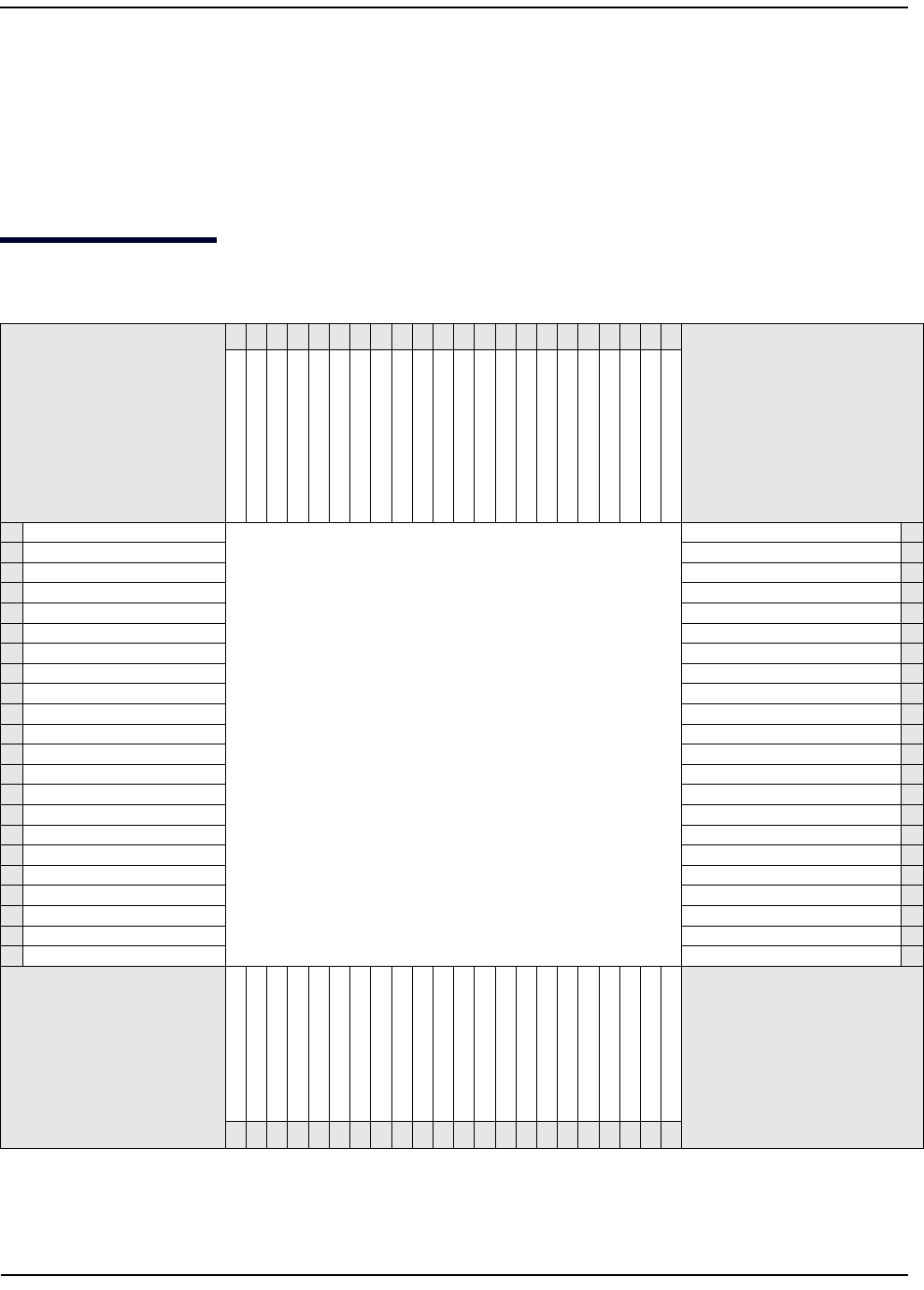
BCM43236 88-Pin QFN Assignments
Figure 8: BCM43236 88-Pin QFN Package
88 87 86 85 84 83 82 81 80 79 78 77 76 75 74 73 72 71 70 69 68 67
VDD
mimophy_core0_ant1_rx
mimophy_core0_ant1_tx
gpio_6
gpio_5
VDDIO
gpio_4
gpio_3
gpio_2
gpio_1
gpio_0
VDD
VDDIO/OTP_VDD
USB_RREF
HSIC_STRB
HSIC_DATA
USB AVDD 1p2
USB_DMNS
USB_DPLS
USB_AVDD3p3
USB_MONCDR
USBAVDD2p5
1 VDDIO
BCM43236 10 x 10 QFN
VDD 66
2sflash_cs_l mimophy_core1_ant1_rx 65
3sflash_q mimophy_core1_ant1_tx 64
4sflash_c VDDIO 63
5sflash_d UART_RX 62
6 mimophy_core0_ant0_tx UART_TX 61
7 mimophy_core0_ant0_rx VDD 60
8VDD VDDPLL/RF_AVDD_1p2 59
9 mimophy_core1_ant0_tx USBLDO_2p5_out 58
10 mimophy_core1_ant0_rx LDO_3p3_in 57
11 VDDIO VREF 56
12 VDD PAREF 55
13 gpio_7 PAREF_CTL1 54
14 jtag_trst_l PAREF_CTL2 53
15 jtag_tdi Ext_por 52
16 jtag_tck xtal_buf_out 51
17 analog_wlan_iqtest_VDD1p2 i_xtal_VDD2p5/o_xtal_VDD2p5 50
18 jtag_tms xtal_in 49
19 jtag_tdo xtal_out 48
20 analog_wlan_iqtest_qp synth_VDD1p2 47
21 analog_wlan_iqtest_qn synth_vco_VDD1p2 46
22 analog_wlan_iqtest_in vreg3p3_VDD3p3 45
analog_wlan_iqtest_ip
Gnd
pa_5g_core1_VDD3p3
PA_5g_core1
tx_5g_core1_VDD1p2
rf_5g_antenna_core1
core1_VDD1p2
rf_2g_antenna_core1
tx_2g_core1_VDD1p2
pa_2g_core1_VDD3p3
PA_2g_core1
pa_5g_core0_VDD3p3
PA_5g_core0
tx_5g_core0_VDD1p2
rf_5g_antenna_core0
core0_VDD1p2
rf_2g_antenna_core0
tx_2g_core0_VDD1p2
pa_2g_core0_VDD3p3
PA_2g_core0
gpiao_GPIO_PAD
rcal_res_ext_core
23 24 25 26 27 28 29 30 31 32 33 34 35 36 37 38 39 40 41 42 43 44

12/20/2010 CTJ5M
CONFIDENTIAL FOR LG INNOTEK CO LTD
BROADCOM 2.4 GHz/5 GHz 802.11n MAC/PHY/Radio Chip
December 17, 2010 • 43236-DS04-R Page 21
®
BCM43236 88-Pin QFN AssignmentsBCM43236 Preliminary Data Sheet
Signals by Pin Number
Table 2: Pin Assignments
Pin Signal Name
1 VDDIO
2sflash_cs_l
3sflash_q
4sflash_c
5sflash_d
6 mimophy_core0_ant0_tx
7 mimophy_core0_ant0_rx
8VDD
9 mimophy_core1_ant0_tx
10 mimophy_core1_ant0_rx
11 VDDIO
12 VDD
13 gpio_7
14 jtag_trst_l
15 jtag_tdi
16 jtag_tck
17 analog_wlan_iqtest_VDD
1p2
18 jtag_tms
19 jtag_tdo
20 analog_wlan_iqtest_qp
21 analog_wlan_iqtest_qn
22 analog_wlan_iqtest_in
23 analog_wlan_iqtest_ip
24 Gnd
25 pa_5g_core1_VDD3p3
26 PA_5g_core1
27 tx_5g_core1_VDD1p2
28 rf_5g_antenna_core1
29 core1_VDD1p2
30 rf_2g_antenna_core1
31 tx_2g_core1_VDD1p2
32 pa_2g_core1_VDD3p3
33 PA_2g_core1
34 pa_5g_core0_VDD3p3
35 PA_5g_core0
36 tx_5g_core0_VDD1p2
37 rf_5g_antenna_core0
38 core0_VDD1p2
39 rf_2g_antenna_core0
40 tx_2g_core0_VDD1p2
41 pa_2g_core0_VDD3p3
42 PA_2g_core0
43 gpiao_GPIO_PAD
44 rcal_res_ext_core
45 vreg3p3_VDD3p3
Pin Signal Name
46 synth_vco_VDD1p2
47 synth_VDD1p2
48 xtal_out
49 xtal_in
50 i_xtal_VDD2p5/
o_xtal_VDD2p5
51 xtal_buf_out
52 Ext_por
53 PAREF_CTL2
54 PAREF_CTL1
55 PAREF
56 VREF
57 LDO_3p3_in
58 USBLDO_2p5_out
59 VDDPLL/RF_AVDD_1p2
60 VDD
61 UART_TX
62 UART_RX
63 VDDIO
64 mimophy_core1_ant1_tx
65 mimophy_core1_ant1_rx
66 VDD
67 USBAVDD2p5
Pin Signal Name
68 USB_MONCDR
69 USB_AVDD3p3
70 USB_DPLS
71 USB_DMNS
72 USB AVDD 1p2
73 HSIC_DATA
74 HSIC_STRB
75 USB_RREF
76 VDDIO/OTP_VDD
77 VDD
78 gpio_0
79 gpio_1
80 gpio_2
81 gpio_3
82 gpio_4
83 VDDIO
84 gpio_5
85 gpio_6
86 mimophy_core0_ant1_tx
87 mimophy_core0_ant1_rx
88 VDD
Pin Signal Name

12/20/2010 CTJ5M
CONFIDENTIAL FOR LG INNOTEK CO LTD
Signal and Pin Descriptions
BROADCOM 2.4 GHz/5 GHz 802.11n MAC/PHY/Radio Chip
December 17, 2010 • 43236-DS04-R Page 22
®
BCM43236 Preliminary Data Sheet
Section 4: Signal and Pin Descriptions
Package Signal Descriptions
The signal name, type, and description of each pin in the BCM43236 88-pin QFN package is listed in Table 3.
The symbols shown under Type indicate pin directions (I/O = bidirectional, I = input, O = output) and the
internal pull-up/pull-down characteristics (PU = weak internal pull-up resistor and PD = weak internal pull-
down resistor), if any. See also Table 4 on page 26 for resistor strapping options.
Table 3: Signal Descriptions
Signal BCM43236 Type Description
Crystal Oscillator
xtal_in 49 I XTAL oscillator input. Connect a 20 MHz, 10 ppm
crystal between the xtal_in and xtal_out pins.
xtal_out 48 O XTAL oscillator output
xtal_buf_out 51 O Buffered XTAL output
Serial Flash Interface
sflash_cs_l 2 O (8 mA-PU) Serial Flash chip select
sflash_q 3 I (8mA-PU) Serial Flash data input
sflash_c 4 O (8 mA-PD) Serial Flash clock
sflash_d 5 O (8 mA) Serial Flash data output
USB Interface
usb_dmns 71 I/O USB interface port D–
usb_dpls 70 I/O USB interface port D+
usb_rref 75 O During USB mode, tie this pin in parallel through
a 100 pF capacitor and a 4 kΩ resistor to ground.
During HSIC mode, tie this pin to a 50Ω resistor
to ground.
hsic_strb 74 O USB HSIC strobe
hsic_data 73 I/O USB HSIC data
usb_moncdr 68 – For test/diagnostic purposes only.
Miscellaneous Signals
rcal_res_ext_core 44 O Reference output, connect to ground via 15k 1%
resistor.
ext_por 52 I External power-on reset (POR) input. Active low.
Allows an optional external power-on reset
circuit to be connected. If installed, the external
POR will override the internal POR.
analog_wlan_iqtest_qp 20 – IQ test pin

12/20/2010 CTJ5M
CONFIDENTIAL FOR LG INNOTEK CO LTD
Package Signal Descriptions
BROADCOM 2.4 GHz/5 GHz 802.11n MAC/PHY/Radio Chip
December 17, 2010 • 43236-DS04-R Page 23
®
BCM43236 Preliminary Data Sheet
analog_wlan_iqtest_qn 21 – IQ test pin
analog_wlan_iqtest_in 22 – IQ test pin
analog_wlan_iqtest_ip 23 – IQ test pin
RF Control Interface
mimophy_core0_ant0_tx 6 O Antenna0 TR Switch controls for core 0. These
pins are also used as strapping options, see
Table 4 on page 26.
mimophy_core0_ant0_rx 7
mimophy_core0_ant1_tx 86 O Antenna1 TR Switch controls for core 0. These
pins are also used as strapping options, see
Table 4 on page 26.
mimophy_core0_ant1_rx 87
mimophy_core1_ant0_tx 9 O Antenna0 TR Switch controls for core 1. These
pins are also used as strapping options, see
Table 4.
mimophy_core1_ant0_rx 10
mimophy_core1_ant1_tx 64 O Antenna1 TR Switch controls for core 1. These
pins are also used as strapping options, see
Table 4.
mimophy_core1_ant1_rx 65
RF Signal Interface
rf_5g_antenna_core0 37 I Chain 0 RF receive input, 5 GHz band
rf_5g_antenna_core1 28 I Chain 1 RF receive input, 5 GHz band
rf_2g_antenna_core0 39 I Chain 0 RF receive input, 2.4 GHz band
rf_2g_antenna_core1 30 I Chain 1 RF receive input, 2.4 GHz band
pa_5g_core0 35 O Chain 0 RF transmit output, 5 GHz band
pa_5g_core1 26 O Chain 1 RF transmit output, 5 GHz band
pa_2g_core0 42 O Chain 0 RF transmit output, 2.4 GHz band
pa_2g_core1 33 O Chain 1 RF transmit output, 2.4 GHz band
JTAG Interface
jtag_trst_l 14 I/O JTAG Reset Input. Resets the JTAG Controller. If
not used, this pin should be pulled low by a 1 kΩ
resistor. This pin is muxed with gpio0.
jtag_tck 16 I/O JTAG Test Clock Input. Used to synchronize JTAG
control and data transfers. If not used, this pin
should be pulled low by a 1 kΩ resistor. This pin
is muxed with btcx_rf_active (Bluetooth
coexistence output, RF active).
jtag_tdi 15 I/O JTAG Test Data Input. Serial data input to the
JTAG TAP controller. Sampled on the rising edge
of TCK. If not used, it may be left unconnected.
This pin is muxed with btcx_tx_conf (Bluetooth
coexistence output, WLAN transmit).
Table 3: Signal Descriptions (Cont.)
Signal BCM43236 Type Description

12/20/2010 CTJ5M
CONFIDENTIAL FOR LG INNOTEK CO LTD
Package Signal Descriptions
BROADCOM 2.4 GHz/5 GHz 802.11n MAC/PHY/Radio Chip
December 17, 2010 • 43236-DS04-R Page 24
®
BCM43236 Preliminary Data Sheet
jtag_tdo 19 I/O JTAG Test Data Output. Serial data output from
the JTAG TAP controller. Sampled on the rising
edge of TCK. If not used, it may be left
unconnected. This pin is muxed with btcx_prisel
(Bluetooth coexistence output, antenna select).
jtag_tms 18 I/O JTAG Mode Select Input. Single control input to
the JTAG TAP controller used to traverse the test
logic state machine. Sampled on the rising edge
of TCK. If not used, it may be left unconnected.
This pin is muxed with btcx_status (Bluetooth
coexistence output, status).
GPIO Interface
gpio_0 78 I/O
(8 mA)
General Purpose I/O pin. This pin is tristated on
power-up and reset. Subsequently, it becomes
an input or an output through software control.
A programmable PU or PD resistor is available
for each GPIO pin. This pin is muxed with
wlan_led (WLAN LED output).
gpio_1 79 I/O General Purpose I/O pin. This pin is muxed with
mimophy_core0_ant_shd (antenna switch
control for the shared [middle] antenna of a 2 of
3 design
[core 0]).
gpio_2 80 I/O General Purpose I/O pin. This pin is muxed with:
• mimophy_core1_ant_shd: antenna switch
control for the shared (middle) antenna of a
2 of 3 design
(core 1).
• btcx_freq: Bluetooth coexistence RF
frequency
gpio_3 81 I/O General Purpose I/O pin.
gpio_4 82 I/O General Purpose I/O pin. This pin is muxed with:
• ext_lna_2g_pu_0: 2.4 GHz band core 0
power amplifier control
• ext_pa_2g_0: 2.4 GHz band core 0 power
amplifier control
• CS: SPI select
gpio_5 84 I/O General Purpose I/O pin. This pin is muxed with:
• ext_lna_2g_pu_1: 2.4 GHz band core 1
power amplifier control
• ext_pa_2g_1: 2.4 GHz band core 1 power
amplifier control
•SCLK: SPI clock
•I2C_SCL: I
2C clock
Table 3: Signal Descriptions (Cont.)
Signal BCM43236 Type Description

12/20/2010 CTJ5M
CONFIDENTIAL FOR LG INNOTEK CO LTD
Package Signal Descriptions
BROADCOM 2.4 GHz/5 GHz 802.11n MAC/PHY/Radio Chip
December 17, 2010 • 43236-DS04-R Page 25
®
BCM43236 Preliminary Data Sheet
gpio_6 85 I/O General Purpose I/O pin. This pin is muxed with:
• ext_lna_5g_pu_0: 5 GHz band core 0 power
amplifier control
• ext_pa_5g_0: 5 GHz band core 0 power
amplifier control)
• SDI: SPI data input
gpio_7 13 I/O General Purpose I/O pin. This pin is muxed with:
• ext_lna_5g_pu_1: 5 GHz band core 1 power
amplifier control
• ext_pa_5g_1: 5 GHz band core 1 power
amplifier control
• SDO: SPI data output
•I2C_SDA: I
2C data
gpiao_gpio_pad 43 – No connect; test only
UART Interface
UART_RX 62 I/O (4 mA PU) UART receive data
UART_TX 61 I/O (4 mA) UART transmit data
Power and Ground
vdd 8, 12, 60, 66,
77, 88
PWR 1.2V supply input for the core logic.
vddio 1, 11, 63, 83 PWR 3.3V supply input for I/O logic
vddio/otp_vdd 76 PWR 3.3V supply input for I/O logic
usbavdd2p5 67 PWR USB analog power supply
usbldo_2p5_out 58 PWR USB LDO output; decouple to ground.
usb_avdd3p3 69 PWR 3.3V supply input to USB interface
usbavdd1p2 72 PWR 1.2V supply input to USB interface
synth_vdd1p2 47 PWR Analog 1.2V supply input
synth_vco_vdd1p2 46 PWR Analog 1.2V supply input
core0_vdd1p2 38 PWR Analog 1.2V supply input
core1_vdd1p2 29 PWR Analog 1.2V supply input
tx_5g_core0_vdd1p2 36 PWR Analog 1.2V supply input
tx_5g_core1_vdd1p2 27 PWR Analog 1.2V supply input
tx_2g_core0_vdd1p2 40 PWR Analog 1.2V supply input
tx_2g_core1_vdd1p2 31 PWR Analog 1.2V supply input
pa_5g_core0_vdd3p3 34 PWR Filtered 3.3V input to internal PA
pa_5g_core1_vdd3p3 25 PWR Filtered 3.3V input to internal PA
pa_2g_core0_vdd3p3 41 PWR Filtered 3.3V input to internal PA
pa_2g_core1_vdd3p3 32 PWR Filtered 3.3V input to internal PA
analog_wlan_iqtest_vdd_1p2 17 PWR 1.2V power supply for IQ test.
Table 3: Signal Descriptions (Cont.)
Signal BCM43236 Type Description

12/20/2010 CTJ5M
CONFIDENTIAL FOR LG INNOTEK CO LTD
Strapping Options
BROADCOM 2.4 GHz/5 GHz 802.11n MAC/PHY/Radio Chip
December 17, 2010 • 43236-DS04-R Page 26
®
BCM43236 Preliminary Data Sheet
Strapping Options
The pins listed in Table 4 are sampled at Power-on Reset (POR) to determine the various operating modes.
Sampling occurs within a few milliseconds following internal POR or deassertion of external POR. After POR,
each pin assumes the function specified in the signal descriptions table. Each pin has an internal pull-up (PU)
or pull-down (PD) resistor that determines the default mode. To change the mode, connect an external PU
resistor to VDDIO or a PD resistor to GND; use 10 kΩ or less (refer to the reference board schematics for further
details).
ldo_3p3_in 57 PWR 3.3V input to RF LDO
vddpll/rf_avdd_1p2 59 O XTAL power reference; decouple to ground.
vreg3p3_vdd3p3 45 PWR Analog 3.3V supply
i_xtal_vdd2p5/o_xtal_vdd2p5 50 PWR 3.3V supply input for I/O logic
vref 56 – VREF; decouple to ground.
paref 55 – PA reference; decouple to ground.
paref_ctl1 54 – PA reference control 1
paref_ctl2 53 – PA reference control 2
gnd_slug H GND Ground
gnd 24 GND Ground
Table 4: Strapping Options
Signal Name Mode Default Description
mimophy_core0_ant0_tx OTP select PU 0: No OTP
1: OTP present
mimophy_core1_ant0_tx SFLASH not
present
PD 0: SFLASH not present
1: SFLASH present
mimophy_core0_ant0_rx ST SFLASH PD 0: SFLASH type is STMicroelectronics
1: SFLASH type is Atmel®
mimophy_core0_ant1_tx USB PHY PU 0: HSIC mode
1: USB PHY mode
mimophy_core0_ant1_rx 120 MHz PU 0: Backplane at 96 (98.4) MHz
1: Backplane at 120 (123) MHz
gpio[7:6] Boot from ROM No pull 00: Remap to RAM; ARM processor to be held at
reset.
01: Boot from ROM unless the ARM needs to be
held at reset.
Table 3: Signal Descriptions (Cont.)
Signal BCM43236 Type Description
12/20/2010 CTJ5M
CONFIDENTIAL FOR LG INNOTEK CO LTD
Electrical Characteristics
BROADCOM 2.4 GHz/5 GHz 802.11n MAC/PHY/Radio Chip
December 17, 2010 • 43236-DS04-R Page 27
®
BCM43236 Preliminary Data Sheet
Section 5: Electrical Characteristics
Absolute Maximum Ratings
Note: Values in this data sheet are design goals and are subject to change based on the results of device
characterization.
Caution! The specifications in Table 5 define levels at which permanent damage to the device can
occur. Functional operation is not guaranteed under these conditions. Operation at absolute
maximum conditions for extended periods can adversely affect the long-term reliability of the device.
Table 5: Absolute Maximum Ratings
Rating Symbol Minimum Maximum Unit
DC supply voltage for core VDDC –0.5 +1.4 V
DC supply voltage for I/O VDDO –0.5 +3.8 V
Voltage on any input or output pin VIMAX, VIMIN –0.5 +3.8a
a. The max voltage requirement is to not exceed VDDO + 0.5V when VDDO < 3.3V.
V
Ambient Temperature (Operating) TA0+65
b
b. The temperature above the shield is 65°C for the TJ to be less than 125°C with a Pout of 15 dBm.
°C
Operating Junction Temperature 125°C TJ– 125 °C
Operating Humidity – – 85 %
Storage Temperature TSTG –40 +125 °C
Storage Humidity – – 60 %
ESD Protection (HBM) VESD – 2000 V

12/20/2010 CTJ5M
CONFIDENTIAL FOR LG INNOTEK CO LTD
Recommended Operating Conditions and DC Characteristics
BROADCOM 2.4 GHz/5 GHz 802.11n MAC/PHY/Radio Chip
December 17, 2010 • 43236-DS04-R Page 28
®
BCM43236 Preliminary Data Sheet
Recommended Operating Conditions and DC Characteristics
Current Consumption from the 3.3V Supply
Current Consumption from the 1.2V Supply
Table 6: Recommended Operating Conditions and DC Characteristics
Element Symbol
Value
UnitMinimum Typical Maximum
DC supply voltage for I/O VDDO 2.97 3.3 3.63 V
DC supply voltage for core and 1.2V analog VDD12 1.14 1.2 1.26 V
Input low voltage (VDDO = 3.3V) VIL ––0.8V
Input high voltage (VDDO = 3.3V) VIH 2.0 – – V
Output low voltage VOL ––0.4V
Output high voltage VOH VDDO – 0.4V – – V
Table 7: Current Consumption from 3.3V Supply
Item Typical Maximum Units
Radio disabled state 29 48 mA
Idle and associated state, PM2 mode 120 148 mA
Active state, TX or RX, 40 MHz channel, maximum
throughput, PM2 mode
462 716 mA
Table 8: Current Consumption from 1.2V Supply
Item Typical Maximum Units
Radio disabled state 47 68 mA
Idle and associated state, PM2 mode 228 296 mA
Active state, TX or RX, 40 MHz channel, maximum
throughput, PM2 mode
510 708 mA

12/20/2010 CTJ5M
CONFIDENTIAL FOR LG INNOTEK CO LTD
HSIC Characteristics
BROADCOM 2.4 GHz/5 GHz 802.11n MAC/PHY/Radio Chip
December 17, 2010 • 43236-DS04-R Page 29
®
BCM43236 Preliminary Data Sheet
HSIC Characteristics
Table 9: HSIC Characteristics
Parameter Symbol Minimum Typical Maximum Unit Comments
HSIC signaling voltage VDD 1.11.21.3V–
I/O voltage input low VIL –0.3 – 0.35 × VDD V–
I/O Voltage input high VIH 0.65 × VDD –V
DD + 0.3 V –
I/O voltage output low VOL ––0.25 × V
DD V–
I/O voltage output high VOH 0.75 × VDD ––V–
I/O pad drive strength OD40 – 60 ΩControlled output
impedance driver
I/O weak keepers IL20 – 70 mA –
I/O input impedance ZI100 – – kΩ–
Total capacitive loada
a. Total Capacitive Load (CL), includes device Input/Output capacitance, and capacitance of a 50Ω PCB trace with
a length of 10 cm.
CL3–14pF–
Characteristic trace
impedance
TI45 50 55 Ω–
Circuit board trace length TL––10cm–
Circuit board trace
propagation skewb
b. Maximum propagation delay skew in STROBE or DATA with respect to each other. The trace delay should be
matched between STROBE and DATA to ensure that the signal timing is within specification limits at the
receiver.
TS––15ps–
STROBE frequencyc
c. Jitter and duty cycle are not separately specified parameters: they are incorporated into the values in the table
above.
FSTROBE 239.988 240 240.012 MHz ± 500 ppm
Slew rate (rise and fall)
STROBE and DATACTslew 0.60 × VDD 1.0 1.2 V/ns Averaged from
30% ~ 70% points
Receiver data setup time
(with respect to STROBE)cTs300 – – ps Measured at the
50% point
Receiver data hold time
(with respect to STROBE)cTb300 – – ps Measured at the
50% point

12/20/2010 CTJ5M
CONFIDENTIAL FOR LG INNOTEK CO LTD
RF Specifications
BROADCOM 2.4 GHz/5 GHz 802.11n MAC/PHY/Radio Chip
December 17, 2010 • 43236-DS04-R Page 30
®
BCM43236 Preliminary Data Sheet
Section 6: RF Specifications
2.4 GHz Band General RF Specifications
Note: Values in this data sheet are design goals and are subject to change based on the results of device
characterization.
Table 10: 2.4 GHz Band General RF Specifications
Item Condition Minimum Typical Maximum Unit
aRxTxTurnaroundTime Including switch time – – 2 μs

12/20/2010 CTJ5M
CONFIDENTIAL FOR LG INNOTEK CO LTD
2.4 GHz Band Receiver RF Specifications
BROADCOM 2.4 GHz/5 GHz 802.11n MAC/PHY/Radio Chip
December 17, 2010 • 43236-DS04-R Page 31
®
BCM43236 Preliminary Data Sheet
2.4 GHz Band Receiver RF Specifications
Table 11: 2.4 GHz Band Receiver RF Specifications
Characteristic Condition Minimum Typical Maximum Unit
Cascaded Noise Figure – – 4.5 – dB
Maximum Receive Levela
a. When using a suitable external switch.
@ 1, 2 Mbps –4 – – dBm
@ 5.5, 11 Mbps –10 – – dBm
@ 54 Mbps –10 – – dBm
Input IP3 Maximum gain – –16 – dBm
Minimum gain – –2 – dBm
LPF 3 dB Bandwidth – 8 8.5 9 MHz
PGA DC Rejection Servo Loop Bandwidth WB mode – 1 – MHz
NB mode 120 Hz – 230 kHz –
LPF DC Rejection Servo Loop Bandwidth WB mode – 500 – kHz
NB mode 120 Hz – 230 kHz –
Maximum Receiver Gain – – 88 – dB
Gain Control Step – – 3 – dB/step
Rx Sensitivity
(10% PER for 4096 octet PSDU) at WLAN
RF port. Defined for default parameters:
GF, 800 ns GI, and non-STBC.
20 MHz channel spacing for all MCS rates
MCS0 OFDM – –91 – dBm
MCS7 OFDM – –74 – dBm
MCS8 OFDM – –88.5 – dBm
MCS15 OFDM – –69 – dBm
40 MHz channel spacing for all MCS rates
MCS0 OFDM – –88 – dBm
MCS7 OFDM – –71 – dBm
MCS8 OFDM – –85.5 – dBm
MCS15 OFDM – –66 – dBm

12/20/2010 CTJ5M
CONFIDENTIAL FOR LG INNOTEK CO LTD
2.4 GHz Band Transmitter RF Specifications
BROADCOM 2.4 GHz/5 GHz 802.11n MAC/PHY/Radio Chip
December 17, 2010 • 43236-DS04-R Page 32
®
BCM43236 Preliminary Data Sheet
2.4 GHz Band Transmitter RF Specifications
2.4 GHz Band Local Oscillator Specifications
Table 12: 2.4 GHz Band Transmitter RF Specifications
Characteristic Condition Minimum Typical Maximum Unit
RF Output Frequency Range – 2400 – 2500 MHz
G band 20 MHz BW – – 16 dBm
40 MHz BW – – 14.5 dBm
Carrier Suppression – 15 – – dBr
TX Spectrum mask @
maximum gain
fc – 22 MHz < f < fc – 11 MHz – – –30 dBr
fc + 11 MHz < f < fc + 22 MHz – – –30 dBr
f < fc – 22 MHz; and f > fc + 22
MHz
–––50dBr
TX Modulation Accuracy
(EVM) at maximum gain
IEEE 802.11b mode – – 35% –
IEEE 802.11g mode – – 5% –
Gain Control Step Size – – 0.25 – dB/step
I/Q Baseband Bandwidth IEEE 802.11b mode – 12 – MHz
IEEE 802.11g mode – 12 – MHz
Amplitude Balancea
a. At a 3 MHz offset from the carrier frequency.
DC input –1 – 1 dB
Phase BalanceaDC input –1.5 – 1.5 °C
Baseband Differential Input
Voltage
Shaped pulse – 0.6 – Vpp
Table 13: 2.4 GHz Band Local Oscillator Specifications
Characteristic Condition Minimum Typical Maximum Unit
VCO Frequency Range – 2412 – 2484 MHz
Reference Input Frequency Range – – 20 – MHz
Clock Frequency Tolerance – – – ±20 ppm
Reference Spurs – – – –34 dBc
Local Oscillator Phase Noise, single-sided from
1 kHz–300 kHz offset
––––86.5dBc/Hz

12/20/2010 CTJ5M
CONFIDENTIAL FOR LG INNOTEK CO LTD
5 GHz Band Receiver RF Specifications
BROADCOM 2.4 GHz/5 GHz 802.11n MAC/PHY/Radio Chip
December 17, 2010 • 43236-DS04-R Page 33
®
BCM43236 Preliminary Data Sheet
5 GHz Band Receiver RF Specifications
Table 14: 5 GHz Band Receiver RF Specificationsa
a. With minimum RF gain.
Characteristic Condition Minimum Typical Maximum Unit
Cascaded Noise Figure Maximum RX gain – 4.5 – dB
Maximum Receive Levela (5.24 GHz) @ 6 Mbps –10 (TBV) – – dBm
Maximum Receive Levela (5.24 GHz) @ 54 Mbps –15 (TBV) – – dBm
Input IP3 Maximum LNA gain – –5 – dBm
Minimum LNA gain – –4 – dBm
LPF 3 dB Bandwidth – – 8.5 – MHz
DC Rejection Servo Loop Bandwidth
(normal operation)
WB mode – 500 – kHz
NB mode 120 Hz – 230 kHz –
Minimum RX Gain – – 15 – dB
Maximum RX Gain – – 92 – dB
Gain Control Step – – 3 – dB/step
IQ Amplitude Balance – – 0.5 – dB
IQ Phase Balance – – 1.5 – °C
Out-of-Band Blocking Performance without RF Band-Pass Filter (–1 dB desensitization):
CW 30 MHz–4300 MHz –10 (TBV) – – dBm
CW 4300 MHz–4800 MHz –25 (TBV) – – dBm
CW 5900 MHz–6400 MHz –25 (TBV) – – dBm
Rx Sensitivity
(10% PER for 4096 octet PSDU) at
WLAN RF port. Defined for default
parameters: GF, 800 ns GI, and non-
STBC.
20 MHz channel spacing for all MCS rates
MCS0 OFDM – –90 – dBm
MCS7 OFDM – –74 – dBm
MCS8 OFDM – –88.5 – dBm
MCS15 OFDM – –69 – dBm
40 MHz channel spacing for all MCS rates
MCS0 OFDM – –87 – dBm
MCS7 OFDM – –71 – dBm
MCS8 OFDM – –86 – dBm
MCS15 OFDM – –66 – dBm

12/20/2010 CTJ5M
CONFIDENTIAL FOR LG INNOTEK CO LTD
5 GHz Band Transmitter RF Specifications
BROADCOM 2.4 GHz/5 GHz 802.11n MAC/PHY/Radio Chip
December 17, 2010 • 43236-DS04-R Page 34
®
BCM43236 Preliminary Data Sheet
5 GHz Band Transmitter RF Specifications
5 GHz Band Local Oscillator Frequency Generator
Specifications
Table 15: 5 GHz Band Transmitter RF Specifications
Characteristic Condition Minimum Typical Maximum Unit
RF Output Frequency Range – 4920 – 5805 MHz
Output Power (EVM-
compliant)
20 MHz BW – – 15 dBm
40 MHz BW – – 14 dBm
Carrier Suppression – – – TBD dBr
TX Spectrum mask
(chip output power = 11 dBm)
f < fc – 11 MHz and f > fc + 11 MHz – – –26 dBc
f < fc – 20 MHz and f > fc + 20 MHz – – –35 dBr
f < fc – 30 MHz and f > fc + 30 MHz – – –40 dBr
TX Modulation Accuracy (EVM) Po = 11 dBm – –25 – dB
TX Modulation Accuracy (EVM) Po = 6 dBm – –33 – dB
Gain Control Step Size – – 2 – dB/step
I/Q Baseband 3 dB Bandwidth – – 12 – MHz
Amplitude Balance DC Input –0.5 – 0.5 dB
Phase Balance DC Input –1.5 – 1.5 °C
Baseband Differential Input
Voltage
––0.7–Vpp
TX Power Ramp Up 90% of final power – – 2 µsec
TX Power Ramp Down 10% of final power – – 2 µsec
Table 16: 5 GHz Band Local Oscillator Frequency Generator Specifications
Characteristic Condition Minimum Typical Maximum Unit
VCO Frequency Range – 4920 – 5805 MHz
Reference Input Frequency Range – – 20 – MHz
Clock Frequency Tolerance – – – ±20 ppm
Reference Spurs – – – –30 dBc
Local Oscillator Integrated Phase
Noise (1 kHz–300 kHz)
4.920 GHz–5.700 GHz – 0.7 – °C
5.725 GHz–5.805 GHz – 1.4 –

12/20/2010 CTJ5M
CONFIDENTIAL FOR LG INNOTEK CO LTD
On-Chip Regulator Power Supply Characteristics
BROADCOM 2.4 GHz/5 GHz 802.11n MAC/PHY/Radio Chip
December 17, 2010 • 43236-DS04-R Page 35
®
BCM43236 Preliminary Data Sheet
On-Chip Regulator Power Supply Characteristics
Table 17: On-Chip Regulator Power Supply Characteristics
Element
Value
UnitMinimum Typical Maximum
2.5V–3.1V PA Reference LDO (default: off)
Vout: 2.5V to 3.1V when output A, B, C and/or D is enabled.
Control Step: 50 mV/step
Input Power Supply 2.97 3.3 3.63 V
Vout (Note 1) Programmable, 50 mV/step 2.5 2.85 3.1 V
Absolute Accuracy –4 – +4 %
Maximum Output Current: A, B, C and D all enabled – – 40 mA
Maximum Output Current: any output A, B, C, or D – – 10 mA
Dropout Voltage 150 – – mV
Startup Time – – 100 µs
Switching ON Time (either A or G)
Note: LDO is already powered.
20 30 100 ns
Switching OFF Time (either A or G)
Note: LDO is already powered.
11.32ns
3.3V–1.2V RF LDO
Input power supply, Vbat 2.97 3.30 3.63 V
Vout (Note 1) Programmable, 50 mV/step 1.2 – 3.0 V
Absolute Accuracy –4 – +4 %
Dropout Voltage 150 – – mV
Maximum Output Current – – 120 mA
Startup time with 100 µs VDD
Ramp
––50µs
3.3V–2.5V USB LDO
Input power supply 2.97 3.30 3.63 V
Vout 2.3 2.5 2.65 V
Absolute accuracy –4 – +4 %
Dropout voltage 150 – – mV
Maximum output current – – 30 mA
Start-up time – – 50 µs
Note: It is required that the input supply be at least 200 mV higher than the output. More headroom is better
for PSRR performance.
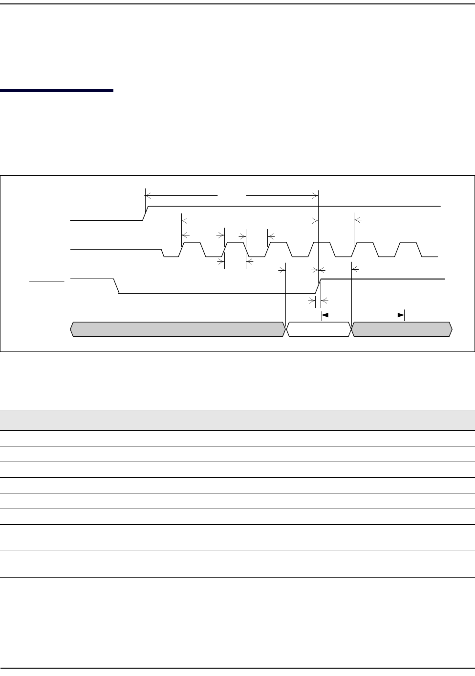
12/20/2010 CTJ5M
CONFIDENTIAL FOR LG INNOTEK CO LTD
Timing Characteristics
BROADCOM 2.4 GHz/5 GHz 802.11n MAC/PHY/Radio Chip
December 17, 2010 • 43236-DS04-R Page 36
®
BCM43236 Preliminary Data Sheet
Section 7: Timing Characteristics
Reset and Clock Timing Diagram
Resets are generated internally by the BCM43236. An optional external Power-On Reset (POR) circuit can be
connected to the active-low Ext_por input pin. The BCM43236 is reset automatically as long as the power
supplies are turned on in the following sequence. 3.3V first, 2.5V second, and 1.2V last.
Figure 9: Timing for the Optional External Power-On Reset
Table 18: Ext_por and Clock Timing
Parameter Description Minimum Typical Maximum Units
t201 OSCIN frequency 19.9995 20.0000 20.0005 MHz
t202 OSCIN high time – 20 – ns
t203 OSCIN low time – 20 – ns
t204 EXT_POR_L low pulse duration 50 – – ms
t207 Configuration valid setup to EXT_POR_L rising 50 – – μs
t208 Configuration valid hold from EXT_POR_L rising 1.7 – 2.8 ms
t209 EXT_POR_L deassertion to normal switch
operation
–3–ms
t210 Reset low hold time after power supplies
stabilize
50 – – ms
Vcc
WPLL_CLK25
(20 MHz)
Ext_por
Configuration
Strap Signals Valid
t201
t202
t203
t204
t205
t206
t207 t208
t209
t210
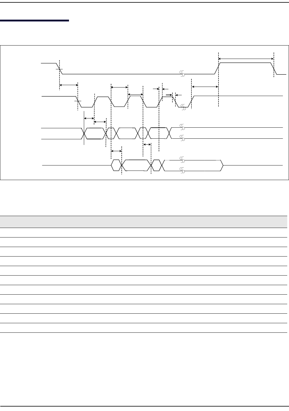
12/20/2010 CTJ5M
CONFIDENTIAL FOR LG INNOTEK CO LTD
Serial Flash Timing Diagram
BROADCOM 2.4 GHz/5 GHz 802.11n MAC/PHY/Radio Chip
December 17, 2010 • 43236-DS04-R Page 37
®
BCM43236 Preliminary Data Sheet
Serial Flash Timing Diagram
Figure 10: Serial Flash Timing Diagram (STMicroelectronics-Compatible)
Table 19: Serial Flash Timing
Parameter Descriptions Minimum Typical Maximum Units
fSCK Serial flash clock frequency – 12.5 66 MHz
tWH Serial flash clock high time 9 – – ns
tWL Serial flash clock low time 9 – – ns
tR, tFa
a. tR and tF are expressed as a slew-rate.
Clock rise and fall timesb
b. Peak-to-peak
TBD – – V/ns
tCSS Chip select active setup time 5 – – ns
tCS Chip select deselect time 100 – – ns
tCSH Chip select hold time 5 – – ns
tSU Data input setup time 2 – – ns
tHData input hold time 5 – – ns
tHO Data output hold time 0 – – ns
tVClock low to output valid – – 8 ns
SFLASH_CS_L
SFLASH_C
SFLASH_Q
SFLASH_D High Impedance High Impedance
tCSS tWL
tWH
tCSH
tCS
tF
tHO
tV
tH
tSU
VALID ON
VALID IN
tR

12/20/2010 CTJ5M
CONFIDENTIAL FOR LG INNOTEK CO LTD
Thermal Information
BROADCOM 2.4 GHz/5 GHz 802.11n MAC/PHY/Radio Chip
December 17, 2010 • 43236-DS04-R Page 38
®
BCM43236 Preliminary Data Sheet
Section 8: Thermal Information
Junction Temperature Estimation and PSIJT Versus ThetaJC
Package thermal characterization parameter Psi-JT (ΨJT) yields a better estimation of actual junction
temperature (TJ) versus using the junction-to-case thermal resistance parameter Theta-JC (θJC). The reason for
this is θJC assumes that all the power is dissipated through the top surface of the package case. In actual
applications, some of the power is dissipated through the bottom and sides of the package. ΨJT takes into
account power dissipated through the top, bottom, and sides of the package. The equation for calculating the
device junction temperature is as follows:
TJ = TT + P
×Ψ
JT
Where:
•T
J = junction temperature at steady-state condition, °C
•T
T = package case top center temperature at steady-state condition, °C
• P = device power dissipation, Watts
•ΨJT = package thermal characteristics (no airflow), °C/W
Package thermal characterization measurements: The temperature above the shield is 65°C for the TJ to be less
than 125°C with a Pout of 15 dBm.
Table 20: 88-Pin QFN Thermal Characteristics
Airflow
0 fpm,
0 mps
100 fpm,
0.508 mps
200 fpm,
1.016 mps
400 fpm,
2.032 mps
600 fpm,
3.048 mps
θJA (°C/W) 20.79 17.55 16.24 15.00 14.34
θJB (°C/W) 3.95––––
θJC (°C/W) 12.44 – – – –
ΨJT (°C/W) 3.51 3.50 3.55 3.59 3.61
Note:
• In the thermal characterizations that were done on the BCM43236 using a 4-layer board, the
temperature at 1 mm above the shield must be no higher than 65°C in order to keep the junction
temperature (TJ) from exceeding 125°C.
• The BCM43236 is designed and rated for operation at a maximum TJ of 125°C.
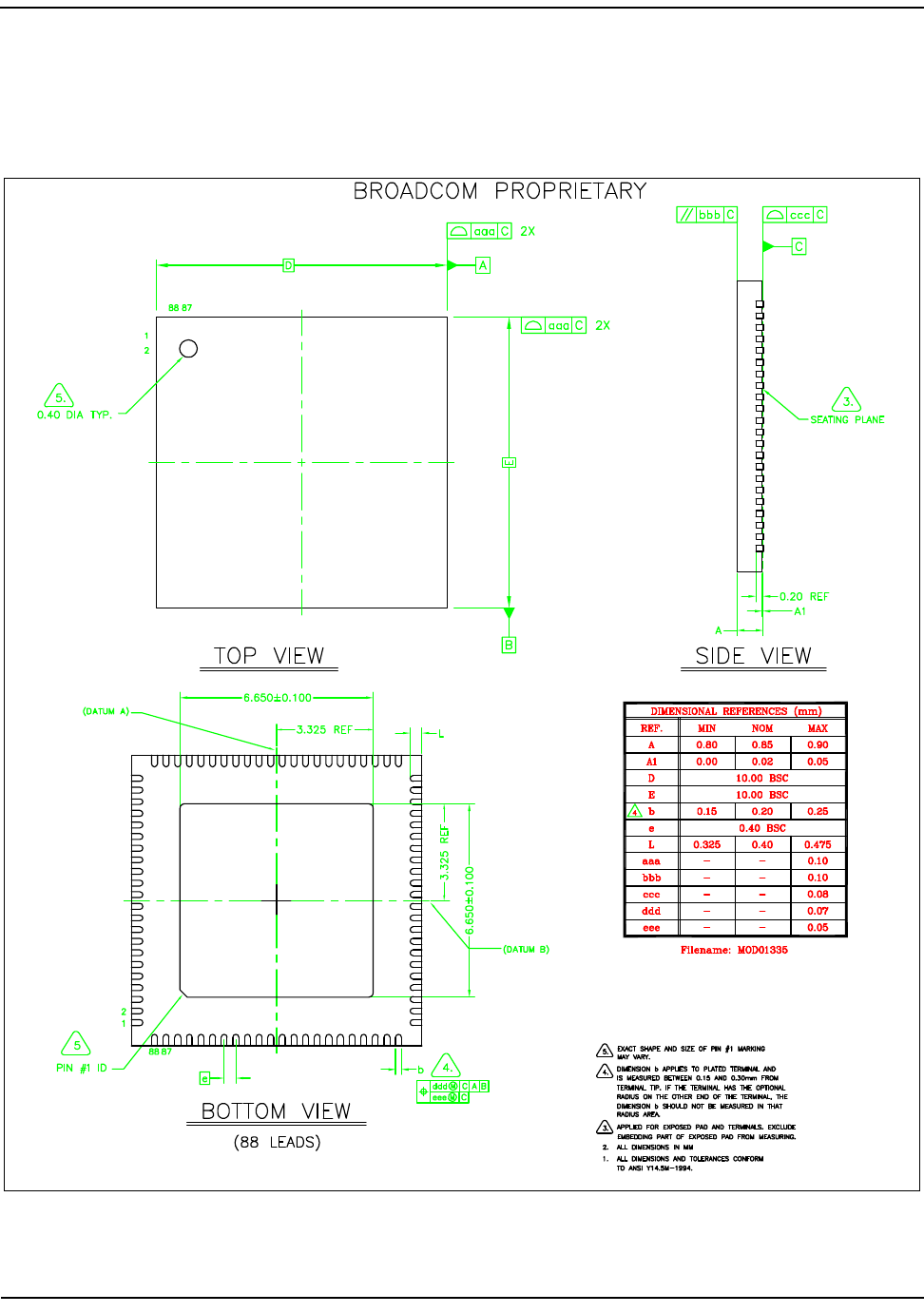
12/20/2010 CTJ5M
CONFIDENTIAL FOR LG INNOTEK CO LTD
Package Information
BROADCOM 2.4 GHz/5 GHz 802.11n MAC/PHY/Radio Chip
December 17, 2010 • 43236-DS04-R Page 39
®
BCM43236 Preliminary Data Sheet
Section 9: Package Information
Figure 11: BCM43236 Mechanical Drawing

12/20/2010 CTJ5M
CONFIDENTIAL FOR LG INNOTEK CO LTD
Ordering Information
BROADCOM 2.4 GHz/5 GHz 802.11n MAC/PHY/Radio Chip
December 17, 2010 • 43236-DS04-R Page 40
®
BCM43236 Preliminary Data Sheet
Section 10: Ordering Information
Table 21: Ordering Information
Part Number Package Temperature @ 1 mm Above the Shield
BCM43236KMLG 10 × 10, 88-pin QFN (RoHs compliant) 0°C to 65°C (32°F to 149°F)

12/20/2010 CTJ5M
CONFIDENTIAL FOR LG INNOTEK CO LTD
®
Phone: 949-926-5000
Fax: 949-926-5203
E-mail: info@broadcom.com
Web: www.broadcom.com
BROADCOM CORPORATION
5300 California Avenue
Irvine, CA 92617
© 2010 by BROADCOM CORPORATION. All rights reserved.
43236-DS04-R December 17, 2010
Broadcom® Corporation reserves the right to make changes without further notice to any products
or data herein to improve reliability, function, or design.
Information furnished by Broadcom Corporation is believed to be accurate and reliable. However,
Broadcom Corporation does not assume any liability arising out of the application or use of this
information, nor the application or use of any product or circuit described herein, neither does it
convey any license under its patent rights nor the rights of others.
BCM43236 Preliminary Data Sheet